JP2010146665A - Resistance change type nonvolatile semiconductor memory - Google Patents
Resistance change type nonvolatile semiconductor memory Download PDFInfo
- Publication number
- JP2010146665A JP2010146665A JP2008324322A JP2008324322A JP2010146665A JP 2010146665 A JP2010146665 A JP 2010146665A JP 2008324322 A JP2008324322 A JP 2008324322A JP 2008324322 A JP2008324322 A JP 2008324322A JP 2010146665 A JP2010146665 A JP 2010146665A
- Authority
- JP
- Japan
- Prior art keywords
- address information
- word line
- redundant
- defective
- level
- Prior art date
- Legal status (The legal status is an assumption and is not a legal conclusion. Google has not performed a legal analysis and makes no representation as to the accuracy of the status listed.)
- Pending
Links
Images
Classifications
-
- G—PHYSICS
- G11—INFORMATION STORAGE
- G11C—STATIC STORES
- G11C8/00—Arrangements for selecting an address in a digital store
- G11C8/08—Word line control circuits, e.g. drivers, boosters, pull-up circuits, pull-down circuits, precharging circuits, for word lines
-
- G—PHYSICS
- G11—INFORMATION STORAGE
- G11C—STATIC STORES
- G11C11/00—Digital stores characterised by the use of particular electric or magnetic storage elements; Storage elements therefor
- G11C11/02—Digital stores characterised by the use of particular electric or magnetic storage elements; Storage elements therefor using magnetic elements
- G11C11/16—Digital stores characterised by the use of particular electric or magnetic storage elements; Storage elements therefor using magnetic elements using elements in which the storage effect is based on magnetic spin effect
- G11C11/165—Auxiliary circuits
- G11C11/1653—Address circuits or decoders
-
- G—PHYSICS
- G11—INFORMATION STORAGE
- G11C—STATIC STORES
- G11C11/00—Digital stores characterised by the use of particular electric or magnetic storage elements; Storage elements therefor
- G11C11/02—Digital stores characterised by the use of particular electric or magnetic storage elements; Storage elements therefor using magnetic elements
- G11C11/16—Digital stores characterised by the use of particular electric or magnetic storage elements; Storage elements therefor using magnetic elements using elements in which the storage effect is based on magnetic spin effect
- G11C11/165—Auxiliary circuits
- G11C11/1659—Cell access
-
- G—PHYSICS
- G11—INFORMATION STORAGE
- G11C—STATIC STORES
- G11C11/00—Digital stores characterised by the use of particular electric or magnetic storage elements; Storage elements therefor
- G11C11/02—Digital stores characterised by the use of particular electric or magnetic storage elements; Storage elements therefor using magnetic elements
- G11C11/16—Digital stores characterised by the use of particular electric or magnetic storage elements; Storage elements therefor using magnetic elements using elements in which the storage effect is based on magnetic spin effect
- G11C11/165—Auxiliary circuits
- G11C11/1673—Reading or sensing circuits or methods
-
- G—PHYSICS
- G11—INFORMATION STORAGE
- G11C—STATIC STORES
- G11C11/00—Digital stores characterised by the use of particular electric or magnetic storage elements; Storage elements therefor
- G11C11/02—Digital stores characterised by the use of particular electric or magnetic storage elements; Storage elements therefor using magnetic elements
- G11C11/16—Digital stores characterised by the use of particular electric or magnetic storage elements; Storage elements therefor using magnetic elements using elements in which the storage effect is based on magnetic spin effect
- G11C11/165—Auxiliary circuits
- G11C11/1675—Writing or programming circuits or methods
-
- G—PHYSICS
- G11—INFORMATION STORAGE
- G11C—STATIC STORES
- G11C11/00—Digital stores characterised by the use of particular electric or magnetic storage elements; Storage elements therefor
- G11C11/02—Digital stores characterised by the use of particular electric or magnetic storage elements; Storage elements therefor using magnetic elements
- G11C11/16—Digital stores characterised by the use of particular electric or magnetic storage elements; Storage elements therefor using magnetic elements using elements in which the storage effect is based on magnetic spin effect
- G11C11/165—Auxiliary circuits
- G11C11/1693—Timing circuits or methods
-
- G—PHYSICS
- G11—INFORMATION STORAGE
- G11C—STATIC STORES
- G11C13/00—Digital stores characterised by the use of storage elements not covered by groups G11C11/00, G11C23/00, or G11C25/00
- G11C13/0002—Digital stores characterised by the use of storage elements not covered by groups G11C11/00, G11C23/00, or G11C25/00 using resistive RAM [RRAM] elements
- G11C13/0004—Digital stores characterised by the use of storage elements not covered by groups G11C11/00, G11C23/00, or G11C25/00 using resistive RAM [RRAM] elements comprising amorphous/crystalline phase transition cells
-
- G—PHYSICS
- G11—INFORMATION STORAGE
- G11C—STATIC STORES
- G11C13/00—Digital stores characterised by the use of storage elements not covered by groups G11C11/00, G11C23/00, or G11C25/00
- G11C13/0002—Digital stores characterised by the use of storage elements not covered by groups G11C11/00, G11C23/00, or G11C25/00 using resistive RAM [RRAM] elements
- G11C13/0007—Digital stores characterised by the use of storage elements not covered by groups G11C11/00, G11C23/00, or G11C25/00 using resistive RAM [RRAM] elements comprising metal oxide memory material, e.g. perovskites
-
- G—PHYSICS
- G11—INFORMATION STORAGE
- G11C—STATIC STORES
- G11C13/00—Digital stores characterised by the use of storage elements not covered by groups G11C11/00, G11C23/00, or G11C25/00
- G11C13/0002—Digital stores characterised by the use of storage elements not covered by groups G11C11/00, G11C23/00, or G11C25/00 using resistive RAM [RRAM] elements
- G11C13/0021—Auxiliary circuits
- G11C13/0023—Address circuits or decoders
- G11C13/0028—Word-line or row circuits
-
- G—PHYSICS
- G11—INFORMATION STORAGE
- G11C—STATIC STORES
- G11C29/00—Checking stores for correct operation ; Subsequent repair; Testing stores during standby or offline operation
- G11C29/04—Detection or location of defective memory elements, e.g. cell constructio details, timing of test signals
- G11C29/08—Functional testing, e.g. testing during refresh, power-on self testing [POST] or distributed testing
- G11C29/12—Built-in arrangements for testing, e.g. built-in self testing [BIST] or interconnection details
- G11C29/44—Indication or identification of errors, e.g. for repair
- G11C29/4401—Indication or identification of errors, e.g. for repair for self repair
-
- G—PHYSICS
- G11—INFORMATION STORAGE
- G11C—STATIC STORES
- G11C29/00—Checking stores for correct operation ; Subsequent repair; Testing stores during standby or offline operation
- G11C29/70—Masking faults in memories by using spares or by reconfiguring
- G11C29/78—Masking faults in memories by using spares or by reconfiguring using programmable devices
- G11C29/785—Masking faults in memories by using spares or by reconfiguring using programmable devices with redundancy programming schemes
- G11C29/789—Masking faults in memories by using spares or by reconfiguring using programmable devices with redundancy programming schemes using non-volatile cells or latches
-
- G—PHYSICS
- G11—INFORMATION STORAGE
- G11C—STATIC STORES
- G11C29/00—Checking stores for correct operation ; Subsequent repair; Testing stores during standby or offline operation
- G11C29/70—Masking faults in memories by using spares or by reconfiguring
- G11C29/78—Masking faults in memories by using spares or by reconfiguring using programmable devices
- G11C29/80—Masking faults in memories by using spares or by reconfiguring using programmable devices with improved layout
- G11C29/81—Masking faults in memories by using spares or by reconfiguring using programmable devices with improved layout using a hierarchical redundancy scheme
-
- G—PHYSICS
- G11—INFORMATION STORAGE
- G11C—STATIC STORES
- G11C29/00—Checking stores for correct operation ; Subsequent repair; Testing stores during standby or offline operation
- G11C29/04—Detection or location of defective memory elements, e.g. cell constructio details, timing of test signals
- G11C29/08—Functional testing, e.g. testing during refresh, power-on self testing [POST] or distributed testing
- G11C29/12—Built-in arrangements for testing, e.g. built-in self testing [BIST] or interconnection details
- G11C2029/1208—Error catch memory
-
- G—PHYSICS
- G11—INFORMATION STORAGE
- G11C—STATIC STORES
- G11C2213/00—Indexing scheme relating to G11C13/00 for features not covered by this group
- G11C2213/30—Resistive cell, memory material aspects
- G11C2213/31—Material having complex metal oxide, e.g. perovskite structure
-
- G—PHYSICS
- G11—INFORMATION STORAGE
- G11C—STATIC STORES
- G11C2213/00—Indexing scheme relating to G11C13/00 for features not covered by this group
- G11C2213/30—Resistive cell, memory material aspects
- G11C2213/32—Material having simple binary metal oxide structure
Landscapes
- Engineering & Computer Science (AREA)
- Computer Hardware Design (AREA)
- Chemical & Material Sciences (AREA)
- Materials Engineering (AREA)
- Crystallography & Structural Chemistry (AREA)
- Microelectronics & Electronic Packaging (AREA)
- For Increasing The Reliability Of Semiconductor Memories (AREA)
Abstract
【課題】不良セルの救済効率を向上する。
【解決手段】本発明の例に関わる抵抗変化型不揮発性半導体メモリは、抵抗変化型記憶素子を含む複数のメモリセルMCが配置されたメモリセルアレイ1Aと、複数のメモリセルMCが接続される複数のワード線WLと、複数の冗長セルRMCが配置された冗長セルアレイ4と、複数の冗長セルRMCが接続される複数の冗長ワード線RWLと、不良セルを救済する制御回路と、を具備し、メモリセルアレイ1A及び冗長セルアレイ4は、カラムアドレス情報CAnに基づいて判別される2つ以上の領域10A,11A,40,41を含み、制御回路は、前記領域10A,11A,40,41毎に、不良セルbMC1が接続されたワード線の一部分WLa<0>と冗長ワード線の一部分RWL<0>とを置き換える。
【選択図】図1An object of the present invention is to improve the repair efficiency of defective cells.
A variable resistance nonvolatile semiconductor memory according to an example of the present invention includes a memory cell array 1A in which a plurality of memory cells MC including a variable resistance storage element are arranged, and a plurality of memory cells MC connected thereto. A word line WL, a redundant cell array 4 in which a plurality of redundant cells RMC are arranged, a plurality of redundant word lines RWL to which a plurality of redundant cells RMC are connected, and a control circuit for relieving defective cells, The memory cell array 1A and the redundant cell array 4 include two or more regions 10A, 11A, 40, and 41 that are discriminated based on the column address information CAn, and the control circuit is provided for each of the regions 10A, 11A, 40, and 41. replacing the defective cell portion of bMC 1 is connected to word line WLa <0> and the redundant word line and a portion RWL <0>.
[Selection] Figure 1
Description
本発明は、抵抗変化型不揮発性半導体メモリに係り、特に、抵抗変化型不揮発性半導体メモリの不良救済技術に関する。 The present invention relates to a variable resistance nonvolatile semiconductor memory, and more particularly to a defect repair technique for a variable resistance nonvolatile semiconductor memory.
近年、携帯電話や携帯型オーディオプレイヤーの普及により、半導体メモリがそれらの電子機器に搭載されている。 In recent years, with the widespread use of mobile phones and portable audio players, semiconductor memories are mounted on these electronic devices.
半導体メモリにおいて、メモリセルアレイ内の不良セルを救済するために、任意の規模の冗長セルアレイが、メモリセルアレイと同一のチップ内に設けられる。この冗長セルアレイ内の冗長セルを、偶発的に発生する不良セルの代わりに用いることによって、メモリセルの不良を救済する手法が、半導体メモリに採用されている(例えば、特許文献1参照)。 In a semiconductor memory, a redundant cell array of an arbitrary scale is provided in the same chip as the memory cell array in order to relieve defective cells in the memory cell array. A technique for remedying a defect in a memory cell by using a redundant cell in the redundant cell array instead of a defective cell that occurs accidentally is employed in a semiconductor memory (for example, see Patent Document 1).
不良セルの救済法としては、2次元に配置された複数のメモリセルに対して、不良セルを含むワード線単位、又は、不良セルを含むビット線単位で、不良セルを救済するライン救済法が一般的である。 As a defective cell remedy method, there is a line remedy method for relieving a defective cell in units of a word line including a defective cell or a bit line including a defective cell with respect to a plurality of memory cells arranged in two dimensions. It is common.
ワード線単位の救済法(以下、ロウ救済法と呼ぶ)においては、不良セルを含むロウアドレス(以下、不良アドレスと呼ぶ)が、フューズなどを用いて、メモリチップ内にあらかじめ記憶されている。そして、外部から入力されたロウアドレスと記憶された不良アドレスとが一致した場合に、不良セルを含むワード線の活性が停止され、冗長セルが接続されたワード線(以下、冗長ワード線と呼ぶ)が活性されることで、不良セルが救済されている。 In a relief method in units of word lines (hereinafter referred to as a row relief method), a row address including a defective cell (hereinafter referred to as a defective address) is stored in advance in a memory chip using a fuse or the like. When the row address input from the outside matches the stored defective address, the activation of the word line including the defective cell is stopped, and the word line to which the redundant cell is connected (hereinafter referred to as a redundant word line). ) Is activated, the defective cell is relieved.
ところで、揮発性半導体メモリ、例えば、DRAM(Dynamic Random Access Memory)においては、リフレッシュ動作が必要である。さらに、DRAMにおいては、リフレシュ動作のサイクル数が記憶容量により規定されているため、同一のサイクル内でリフレッシュ動作の対象となるメモリセル数が決められているという制約がある。このため、DRAMでは、メモリセルアレイ内の1つのワード線を、部分的に活性化させることは、その動作の仕様上不可能である。 By the way, a volatile semiconductor memory, for example, DRAM (Dynamic Random Access Memory), requires a refresh operation. Further, in the DRAM, since the number of cycles of the refresh operation is defined by the storage capacity, there is a restriction that the number of memory cells to be refreshed in the same cycle is determined. For this reason, in the DRAM, it is impossible to partially activate one word line in the memory cell array because of its operation specifications.
すなわち、DRAMにおいては、リフレシュサイクルの仕様と動作の整合性を確保しなければならないため、1本のワード線に含まれた不良セルの数がたとえ1つであっても、そのワード線は1本の冗長ワード線と置換される。このため、メモリセルアレイ内に、ロウアドレス(ワード線)が異なる2つの不良セルを救済する場合、2本の冗長ワード線が必要になる。
このように、DRAMに対してロウ救済法を用いる場合、ワード線に接続される不良セルの数に関わらず、不良セルが接続されたワード線の本数と同数の冗長ワード線が必要となる。
That is, in a DRAM, it is necessary to ensure the consistency between the refresh cycle specification and the operation, so even if the number of defective cells included in one word line is one, the word line is 1 It is replaced with a redundant word line. For this reason, when two defective cells having different row addresses (word lines) are relieved in the memory cell array, two redundant word lines are required.
As described above, when the row repair method is used for the DRAM, the same number of redundant word lines as the number of word lines to which the defective cells are connected are required regardless of the number of defective cells connected to the word lines.
この場合、不良セルの数が、記憶容量の増大やメモリセルの微細化に伴って増加すると、搭載すべき冗長ワード線(冗長セル数)も増加する。つまり、メモリの大容量化や微細化に伴う不良セルの増加に対し、不良セルの救済効率の向上は、チップ面積の増大及び製造コストの増加を引く起こす可能性がある。 In this case, when the number of defective cells increases as the storage capacity increases or the memory cells become finer, the number of redundant word lines (number of redundant cells) to be mounted also increases. In other words, an increase in defective cell remedy efficiency with an increase in memory capacity and miniaturization may cause an increase in chip area and manufacturing cost.
DRAMの代替として期待される半導体メモリ、例えば、MRAM(Magnetoresistive Random Access Memory)は、リフレシュ動作を必要としないため、上記のリフレッシュ動作に対する制約を排除することが可能であり、より救済効率の高いロウ救済法の実現が望まれている。
本発明は、不良セルの救済効率を向上できる技術を提案する。 The present invention proposes a technique capable of improving the repair efficiency of defective cells.
本発明の例に関わる不揮発性半導体メモリは、抵抗変化型記憶素子を含む複数のメモリセルがマトリクス状に配置されたメモリセルアレイと、前記複数のメモリセルが接続され、第1の方向に延在する複数のワード線と、前記メモリセルアレイの近傍に配置され、前記ワード線を活性化するロウデコーダと、前記メモリセルアレイ内に含まれる不良セルの代わりに用いられる複数の冗長セルが配置された冗長セルアレイと、前記複数の冗長セルが接続され、前記第1の方向に延在する複数の冗長ワード線と、前記冗長セルアレイの近傍に配置され、前記冗長ワード線を活性化する冗長ロウデコーダと、不良セルが接続されたワード線を示す不良アドレス情報が記憶され、入力されたアドレス情報と前記不良アドレス情報とが一致した場合に、前記不良セルを救済する制御回路と、を具備し、前記メモリセルアレイ及び前記冗長セルアレイは、カラムアドレス情報に基づいて判別され、前記第1の方向に分割された少なくとも2つ以上の領域をそれぞれ含み、前記制御回路は、前記領域毎に、前記不良セルが接続された前記ワード線の一部分と前記冗長ワード線の一部分とを置き換えて、その置き換えられた冗長ワード線を前記冗長ロウデコーダに活性化させる、ことを備える。 A nonvolatile semiconductor memory according to an example of the present invention includes a memory cell array in which a plurality of memory cells including a resistance change type storage element are arranged in a matrix, and the plurality of memory cells are connected and extend in a first direction. A plurality of word lines, a row decoder arranged in the vicinity of the memory cell array and activating the word line, and a plurality of redundant cells used in place of defective cells included in the memory cell array. A cell array; a plurality of redundant word lines connected to the plurality of redundant cells; and extending in the first direction; a redundant row decoder disposed in the vicinity of the redundant cell array and activating the redundant word line; When defective address information indicating a word line to which a defective cell is connected is stored and the input address information matches the defective address information, A control circuit for relieving a defective cell, wherein the memory cell array and the redundant cell array each include at least two regions that are determined based on column address information and divided in the first direction. The control circuit replaces a part of the word line to which the defective cell is connected and a part of the redundant word line for each region, and activates the replaced redundant word line in the redundant row decoder. To be prepared.
本発明の例によれば、不良セルの救済効率を向上できる。 According to the example of the present invention, the repair efficiency of defective cells can be improved.
以下、図面を参照しながら、本発明の例を実施するための最良の形態について詳細に説明する。 The best mode for carrying out an example of the present invention will be described below in detail with reference to the drawings.
[第1の実施形態]
以下、図1乃至図8を参照して、本発明の第1の実施形態について説明する。
[First Embodiment]
Hereinafter, a first embodiment of the present invention will be described with reference to FIGS.
(1) 基本構成
図1及び図2を用いて、本発明の第1の実施形態に関わる抵抗変化型不揮発性半導体メモリの基本構成について説明する。
(1) Basic configuration
A basic configuration of the variable resistance nonvolatile semiconductor memory according to the first embodiment of the present invention will be described with reference to FIGS. 1 and 2.
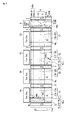
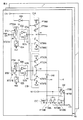
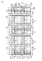
図1は、本実施形態に係る抵抗変化型不揮発性半導体メモリにおける、メモリセルアレイ及びその近傍に配置される回路の構成を示している。 FIG. 1 shows a configuration of a memory cell array and circuits arranged in the vicinity thereof in the variable resistance nonvolatile semiconductor memory according to the present embodiment.
図1に示す例では、4つのメモリセルアレイ1A〜1Dが設けられている。但し、メモリセルアレイは1つでも良い。
In the example shown in FIG. 1, four
メモリセルアレイ1A〜1Dは、抵抗変化型記憶素子を用いた複数のメモリセルMCから構成されている。複数のメモリセルMCは、メモリセルアレイ1A〜1D内に、アレイ状に配置されている。
メモリセルアレイ1A〜1D内には、複数のワード線WL及び複数のビット線BLが設けられている。図1において、ワード線WLは、例えば、Y方向(第1の方向)に延在し、ビット線BLは、例えば、X方向(第2の方向)に延在している。1本のワード線WLには、Y方向に配列された複数のメモリセルMCが接続されている。1本のビット線BLには、X方向に配列された複数のメモリセルMCが共通に接続される。本実施形態においては、1本のワード線WLに共通に接続された複数のメモリセルのことを、メモリセル群ともよぶ。メモリセルアレイ1A〜1Dの内部構成の具体例について、後述する。
The
In the
メモリセルアレイ1A〜1D内における各メモリセルMCの位置は、チップ内に入力されるアドレス情報が含むロウアドレス情報及びカラムアドレス情報によって、示される。ロウアドレス情報が含む全ビットによって、1本のワード線が示され、カラムアドレス情報が含む全ビットによって、1本のビット線BLが示される。
The position of each memory cell MC in the
メモリセルアレイ1A〜1DのY方向に隣接して、ロウデコーダ2A〜2Dがそれぞれ配置されている。ロウデコーダ2A〜2Dは、メモリセルアレイ1A〜1Dのそれぞれに対応して、設けられる。ロウデコーダ2A〜2Dは、外部から入力されたアドレス情報に基づいて、ワード線WLを選択し、そのワード線を活性化する。
また、各メモリセルアレイ1A〜1DのX方向に隣接して、センスアンプ3が配置されている。センスアンプ3は、アドレス情報に基づいて、選択されたメモリセルからビット線BLに読み出された信号(データ)を増幅し、その信号を検知する。
A
図1に示す例では、各メモリセルアレイ1A〜1DのX方向の両端に、センスアンプ3が配置され、1つのメモリセルアレイに対して、2つのセンスアンプ3が接続されている。これによって、メモリセルに記憶されたデータを、メモリセルアレイの両端から読み出せる。この場合、2つのメモリセルアレイ間に配置されたセンスアンプ3は、2つのメモリセルアレイによって共通に用いられる。
In the example shown in FIG. 1,
冗長セルアレイ4は、センスアンプ3を介して、メモリセルアレイ1DのX方向に隣接して設けられる。冗長セルアレイ4内には、不良セルを救済のために用いられる複数の冗長セルRMCが設けられている。また、冗長セルアレイ内には、Y方向に延在する冗長ワード線RWLとX方向に延在する冗長ワード線RBLとが設けられている。
The
冗長セルRMCは、メモリセルMCと同様の構成を有する。冗長セルRMCは、メモリセルMCとワード線WLとの接続関係と同様の構成で、冗長ワード線RWLに接続される。また、冗長セルRMCは、メモリセルMCとビット線BLとの接続関係と同様の構成で、冗長ビット線BLに接続される。尚、1本の冗長ワード線RWLに接続される冗長セルRMCの個数は、1本のワード線WLに接続されるメモリセルMCの個数と同じである。 The redundant cell RMC has a configuration similar to that of the memory cell MC. The redundant cell RMC is connected to the redundant word line RWL with the same configuration as the connection relationship between the memory cell MC and the word line WL. The redundant cell RMC is connected to the redundant bit line BL with the same configuration as the connection relationship between the memory cell MC and the bit line BL. The number of redundant cells RMC connected to one redundant word line RWL is the same as the number of memory cells MC connected to one word line WL.
冗長ワード線WRLは、冗長ロウデコーダ5に接続される。
冗長ロウデコーダ5は、冗長セルアレイ4のY方向に隣接して、配置されている。冗長ロウデコーダ2A〜2Dは、不良セルの代わりに冗長セルが用いられる場合に、冗長ワード線RWLを活性化する。
冗長セルアレイ4のX方向に両端には、メモリセルアレイ1A〜1Dと同様に、2つのセンスアンプ3が設けられている。そして、その一方のセンスアンプ3は、メモリセルアレイ1Dと共有される。冗長ビット線RBLは、センスアンプ3に接続される。
Redundant word line WRL is connected to
The
Similar to the
メモリセルアレイ1A〜1D内に不良セルbMC1,bMC2が存在した場合、後述の制御回路によって、不良セルを含むワード線WLa,WLcと冗長ワード線RWLとが、論理的に置き換えられる。これによって、不良セルbMC1,bMC2が救済される。具体的には以下のとおりである。
When defective cells bMC 1 and bMC 2 exist in
不良セルのアドレス情報(以下、不良アドレス情報と呼ぶ)は、チップのテスト工程時に予め検出され、チップ内の制御回路内に記憶される。
そして、チップに対する書き込み又は読み出し動作時において、アドレス情報が入力されたとき、その入力されたアドレス情報は、制御回路によって、チップ内に予め記憶された不良アドレス情報と比較される。その比較の結果、入力されたアドレス情報が、不良セルbMC1,bMC2(図1中の×印)を含むワード線WLa,WLcを示すアドレス情報と一致すると、制御回路によって判定された場合、その制御回路は、冗長ロウデコーダ5に、冗長セルアレイ4内の冗長ワード線RWLを不良セルが含まれるワード線の代わりに活性化させる。
このように、本実施形態の抵抗変化型不揮発性半導体メモリにおいて、不良セルの救済は、ワード線単位で行われるロウ救済法が採用されている。
The defective cell address information (hereinafter referred to as defective address information) is detected in advance during the chip testing process and stored in a control circuit in the chip.
When address information is input during a write or read operation to the chip, the input address information is compared with defective address information stored in advance in the chip by the control circuit. When the control circuit determines that the input address information matches the address information indicating the word lines WLa and WLc including the defective cells bMC 1 and bMC 2 (x marks in FIG. 1) as a result of the comparison, The control circuit causes the
As described above, in the variable resistance nonvolatile semiconductor memory according to the present embodiment, the row repair method is employed in which defective cells are repaired in units of word lines.
本実施形態の抵抗変化型不揮発性半導体メモリにおいて、メモリセルアレイ内に含まれる不良セルの救済(ワード線の置換)は、メモリセルアレイ1A〜1Dが2つ以上に分割され、その分割された領域10A〜10D,11A〜11Dを対応させて、制御される。図1においては、各メモリセルアレイ1A〜1Dが、2つの領域10A〜10D,11A〜11Dに分割された例を示している。
In the variable resistance nonvolatile semiconductor memory according to the present embodiment, defective cell included in the memory cell array (replacement of word lines) is divided into two or more
本実施形態において、メモリセルアレイ1A〜1Dは、カラムアドレス情報CAnに基づいた論理的な領域10A〜10D,11A〜11Dに分割される。以下、分割された論理的な領域のことを、セグメントと呼ぶ。各セグメント10A〜10D,11A〜11Dは、カラムアドレス情報CAnに基づいて分割されるため、メモリセルアレイ1A〜1Dは、ワード線の延在方向(Y方向)に分割された領域になっている。そして、1つのメモリセルアレイにおいて、2つのセグメントはY方向に互いに隣接している。
In the present embodiment, the
セグメント10A〜10D,11A〜11Dは、例えば、カラムアドレス情報が含むn番目のビットCAnに基づいて、判別される。例えば、セグメントの判別は、カラムアドレス情報の最上位又は最下位の1ビットが用いられる。本実施形態においては、セグメントの判別は、カラムアドレス情報の最上位ビットを用いる場合を例として、説明する。
第1のセグメント10A〜10Dと、第2のセグメント11A〜11Dとが、各メモリセルアレイ1A〜1D内に設定される。第1のセグメント10A〜10Dはカラムアドレス情報CAn=“0”によって、判別される。第2のセグメント11A〜11Dは、カラムアドレス情報CAn=“1”によって、判別される。
また、メモリセルアレイ1A〜1Dと同様に、冗長セルアレイ4に対して、カラムアドレス情報CAn=“0”,“1”によって判別される2つのセグメント40,41が、設定される。
The
Similarly to the
図1に示す例において、ワード線WLa,WLcは、カラムアドレス情報CAnに基づいてセグメントが設定されていることに伴って、第1のセグメント10A〜10Dに配置される一部分WLa<0>,WLc<0>と第2のセグメント11A〜11Dに配置される一部分WLa<1>,WLc<1>とに論理的に分割される。
In the example shown in FIG. 1, the word lines WLa and WLc have portions WLa <0> and WLc arranged in the
そして、不良セルを救済する場合に、論理的に分割された部分毎WLa<0>,WLc<0>,WLa<1>,WLc<1>毎に、救済の単位として、それぞれ個別に制御され、ワード線の一部分と冗長ワード線の一部分とが置き換えられる。これによって、メモリセルアレイ1A〜1D内の不良セルが、救済される。
When repairing a defective cell, each logically divided portion WLa <0>, WLc <0>, WLa <1>, WLc <1> is individually controlled as a repair unit. A part of the word line is replaced with a part of the redundant word line. As a result, the defective cells in the
例えば、メモリセルアレイ1Aにおいて、ワード線WLaは、不良セルbMC1を含んでいる。不良セルbMC1は、カラムアドレス情報CAn=“0”に対応するセグメント10A内に存在し、1本のワード線WLaにおけるセグメント10A内に設けられている部分WLa<0>に、接続されている。
For example, in the
入力されたアドレス情報(ロウ/カラムアドレス情報)が、不良セルが接続されたワード線WLaを示し、不良セルが存在するセグメント10Aを示す場合、そのワード線WLaのセグメント10A内に配置された部分(第1の部分)WLa<0>は不活性にされる。
そして、冗長セルアレイ4において、そのカラムアドレス情報CAn=“0”に基づいて、1本の冗長ワード線RWLのうちセグメント41に配置された部分RWL<0>が、不良セルが接続されたワード線WLaの一部分WLa<0>の代わりに、冗長ロウデコーダ5によって活性化される。
When the input address information (row / column address information) indicates the word line WLa to which the defective cell is connected and indicates the
In the
これによって、不良セルを含むワード線WLaの一部分WLa<0>が、冗長ワード線RWLの一部分RWL<0>と置き換えられる。それゆえ、ワード線WLaの一部分WLa<0>に接続された不良セルbMC1が、救済される。 As a result, a part WLa <0> of the word line WLa including the defective cell is replaced with a part RWL <0> of the redundant word line RWL. Therefore, the defective cell bMC 1 connected to the part WLa <0> of the word line WLa is relieved.
また、カラムアドレス情報CAn=“1”に対応するメモリセルアレイ1Aのセグメント11A内において、ワード線WLaは不良セルを含まない。この場合、セグメント11Aに配置されるワード線WLaの一部分(第2の部分)WLa<1>は、セグメント41に配置される冗長ワード線RWL<1>と置換されない。つまり、チップの動作時に入力されたアドレス情報において、ロウアドレス情報は不良セルbMC1が接続されたワード線WLaを示し、且つ、カラムアドレス情報CAnはそのワード線WLaのうち不良セルが存在していないセグメント11Aを示す場合、そのワード線WLa(ワード線WLaの一部分WLa<1>)は、アドレス情報に基づいて、ロウデコーダ2Aによって活性化される。そして、ワード線WLaの部分WLa<1>に接続された正常なメモリセルは、通常どおりに動作(アクセス)の対象となる。
In addition, in the
メモリセルアレイ1C内に含まれる不良セルbMC2は、メモリセルアレイ1A内に含まれる不良セルbMC1と同様の手法によって、冗長セルアレイ4内の冗長セルを用いて、救済される。
すなわち、不良セルbMC2が接続されたワード線WLcにおいて、入力されたアドレス情報が含むカラムアドレス情報CAn=“1”に基づいて、そのワード線WLcは、セグメント11Cに配置される部分WLc<1>が、冗長ワード線RWLのセグメント41に配置される部分RWL<1>と置き換えられ。それゆえ、ワード線WLcは不活性化され、冗長ワード線RWLは、冗長ロウデコーダ5によって活性化される。
また、カラムアドレス情報CAn=“0”に対応しているワード線WLcの部分WLc<1>は、不良セルを含まないので、アクセス(書き込み/読み出し)を要求するロウ/カラムアドレス情報が入力されたとき、そのワード線WLcは通常どおりにロウデコーダ2Cによって、活性化される。
Defective cell bMC 2 included in the memory cell array. 1C, in the same manner as defective cell bMC 1 included in the
That is, in the defective cell bMC 2 are connected a word line WLc, based on the column address information CAn = "1" including address information input, the word line WLc is part WLc <1 disposed
Further, since the portion WLc <1> of the word line WLc corresponding to the column address information CAn = “0” does not include a defective cell, row / column address information for requesting access (write / read) is input. Then, the word line WLc is activated by the
また、上述のように、冗長セルアレイ4も、2つのセグメント40,41に分割されて、制御される。そのため、1本の冗長ワード線RWLを、各セグメントに対応した2つの部分RWL<0>,RWL<1>毎に、不良セルが接続されたワード線の置き換えに用いることができる。つまり、不良セルbMC1,bMC2が存在するセグメントが異なっていれば、1本の冗長ワード線RWLを用いて、2本のワード線が含む不良セルを救済できる。よって、1本の冗長ワード線を用いた不良セルの救済自由度は、“2”になる。例えば、冗長セルアレイ4が8本の冗長ワード線を有し、図1に示すように、メモリセルアレイ1A〜1D及び冗長セルアレイ4が、1ビット分のカラムアドレス情報CAnに基づいて設定された2つのセグメント10A〜10D,11A〜11Dを有する場合、図1に示される半導体メモリの救済自由度は、“16”になる。
As described above, the
このように、ロウ救済法において、カラムアドレス情報CAnに基づいて、メモリセルアレイ1A〜1Dが複数のセグメント10A,11Aに分割されることによって、不良セルの救済効率を向上できる。
As described above, in the row repair method, the
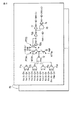
また、上述のように、本実施形態においては、カラムアドレス情報CAnに基づいて、各メモリセルアレイ1A〜1D内に、セグメントを設定し、それらを判別している。このため、カラムアドレス情報が含むビット数に応じて、セグメントの個数を規定できるので、3つ以上のセグメントを1つのメモリセルアレイに対して設定することができる。
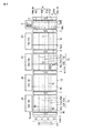
図2に示す例では、2ビット分のカラムアドレス情報CAn,CA(n−1)を利用して、1つのメモリセルアレイ1A〜1C内に、4つのセグメント10A〜13A,10C〜13Cが設定されている。この構成において、不良セルの救済時に、1本のワード線WL及び1本の冗長ワード線RWLは、論理的に4つに分割されて、制御される。
そして、不良セルがアクセスの対象となった場合、分割された各部分を救済の単位として、ワード線WLa<0>と冗長ワード線RWL<0>とが置き換えられる。これによって、冗長ワード線が活性化され、ワード線WLaの一部分WL<0>に含まれる不良セルが、救済される。これと同様に、ワード線WLcの一部分WLc<3>は、冗長ワード線の一部分RWL<3>と置き換えられる。
また、不良セルを含まないセグメント11A〜13A,10C〜12Cにおいて、不良セルを含むワード線WLa,WLcは、アクセスの対象として使用され、ロウデコーダ2A,2Cによって、活性化される。
Further, as described above, in the present embodiment, segments are set in each of the
In the example shown in FIG. 2, four
When a defective cell becomes an access target, the word line WLa <0> and the redundant word line RWL <0> are replaced with each divided portion as a unit of relief. As a result, the redundant word line is activated and the defective cell included in the part WL <0> of the word line WLa is relieved. Similarly, a part WLc <3> of the word line WLc is replaced with a part RWL <3> of the redundant word line.
In the
尚、カラムアドレス情報の全ビット数を用いた場合には、メモリセルアレイ1A〜1Dは、ビット線の本数と同数のセグメントを有し、1つのメモリセル(不良セル)単位での、不良セルの救済が可能となる。
When the total number of bits of the column address information is used, the
このように、メモリセルアレイに設定するセグメント数を多くする、つまり、ワード線の分割数を大きくすることで、不良セルの救済自由度を向上できる。尚、好ましい態様としては、メモリセルアレイ1A〜1Dは、2〜16のセグメントに分割されることが好ましい。
Thus, by increasing the number of segments set in the memory cell array, that is, by increasing the number of divisions of the word lines, the degree of freedom for repairing defective cells can be improved. In a preferred embodiment, the
さらに、本実施形態においては、セグメントの設定及びその判別に、カラムアドレス情報を用いている。それゆえ、セグメントの設定及び判別のために、新たな信号をチップの制御信号に付加する必要はなく、複雑な回路を用いる必要もない。よって、簡便な構成によって、不良セルの救済効率を向上できる。 Furthermore, in this embodiment, column address information is used for segment setting and determination. Therefore, it is not necessary to add a new signal to the control signal of the chip and to use a complicated circuit for segment setting and discrimination. Therefore, the repair efficiency of defective cells can be improved with a simple configuration.
以上のように、本発明の第1の実施形態において、メモリセルアレイ1A〜1Dは、カラムアドレス情報CAnに基づいて、ワード線WLの延在方向(Y方向)に2つ以上の領域(セグメント)に論理的に分割される。不良セルを救済する際、不良セルを含むワード線は、カラムアドレス情報に基づいて、セグメントに配置されている部分毎に制御される。そして、その不良セルを含んでいるワード線において、不良セルを含んでいるセグメントに対応する部分(メモリセル群)が、そのセグメントに対応する冗長ワード線の部分に置き換えられる。これによって、不良セルは救済される。また、不良セルを含んでいるワード線において、不良セルを含まないセグメントに配置されたワード線の一部分(メモリセル群)は、通常どおりに用いられる。
このように、1本のワード線において、それぞれ異なるセグメントに配置される部分は、救済の単位として、独立に扱われる。
As described above, in the first embodiment of the present invention, the
As described above, in one word line, portions arranged in different segments are treated independently as a unit of relief.
それゆえ、本実施形態のように、不良セルを救済することによって、チップに搭載される冗長ワード線の本数、換言すると、冗長セルの個数の増加及び冗長セルアレイの占有面積の増加を伴わないで、救済の自由度が増加する。 Therefore, as in the present embodiment, by repairing a defective cell, the number of redundant word lines mounted on the chip, in other words, without increasing the number of redundant cells and the occupied area of the redundant cell array, is not accompanied. , The relief freedom increases.
したがって、本発明の第1の実施形態に係る抵抗変化型不揮発性半導体メモリによれば、不良セルの救済の自由度を向上でき、メモリセルアレイ内の不良セルの救済効率を向上できる。 Therefore, according to the variable resistance nonvolatile semiconductor memory according to the first embodiment of the present invention, the degree of freedom in repairing a defective cell can be improved, and the repair efficiency of the defective cell in the memory cell array can be improved.
(2) 具体例
(a) 回路構成
図3乃至図7を用いて、本実施形態に係る抵抗変化型不揮発性半導体メモリのより具体的な構成例について説明する。
(2) Specific examples
(A) Circuit configuration
A more specific configuration example of the variable resistance nonvolatile semiconductor memory according to the present embodiment will be described with reference to FIGS. 3 to 7.
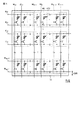
図3は、1つのメモリセルアレイ1Aの内部構成の一例を示している。
図3に示すように、複数のメモリセルMCは、X方向及びY方向に沿って、メモリセルアレイ1A内にアレイ状に配置される。また、図3に示すように、メモリセルアレイ1A内には、複数のビット線BL0〜BLm−1及び複数のワード線WL0〜WLn−1が設けられている。
FIG. 3 shows an example of the internal configuration of one
As shown in FIG. 3, the plurality of memory cells MC are arranged in an array in the
複数のビット線BL0〜BLm−1は、X方向に沿って延在し、Y方向に並んで配置されている。例えば、ビット線BL0及びビット線BL1のように、メモリセルMCの一端及び他端に接続された2本のビット線は、一組のビット線対をなしている。複数のワード線WL0〜WLn−1は、Y方向に沿って延在し、X方向に並んで配置されている。 The plurality of bit lines BL 0 to BL m−1 extend along the X direction and are arranged side by side in the Y direction. For example, like the bit line BL 0 and the bit line BL 1 , two bit lines connected to one end and the other end of the memory cell MC form a set of bit line pairs. The plurality of word lines WL 0 to WL n−1 extend along the Y direction and are arranged side by side in the X direction.
Y方向に沿って配列される複数のメモリセルMCは、一組のビット線対に共通に接続されている。X方向に沿って配列される複数のメモリセルMCは、1本のワード線に共通に接続される。 The plurality of memory cells MC arranged along the Y direction are commonly connected to a set of bit line pairs. A plurality of memory cells MC arranged along the X direction are commonly connected to one word line.
各メモリセルMCは、例えば、1つの抵抗変化型記憶素子MTJと1つの電界効果トランジスタTrとから構成されている。 Each memory cell MC includes, for example, one resistance change type storage element MTJ and one field effect transistor Tr.
メモリセルMC内の抵抗変化型記憶素子MTJは、データの記憶を担う。例えば、本実施形態の抵抗変化型不揮発性半導体メモリが、磁気ランダムアクセスメモリ(MRAM:Magnetoresistive Random Access Memory)である場合には、抵抗変化型記憶素子MTJは、磁気抵抗効果素子である。磁気抵抗効果素子MTJは、データを不揮発に記憶する。 The resistance change type storage element MTJ in the memory cell MC is responsible for storing data. For example, when the variable resistance nonvolatile semiconductor memory according to the present embodiment is a magnetic random access memory (MRAM), the variable resistance memory element MTJ is a magnetoresistive effect element. The magnetoresistive element MTJ stores data in a nonvolatile manner.
磁気抵抗効果素子MTJの基本的な構造は、例えば、磁化方向が不変な第1の磁性層(磁化不変層)と、磁化方向が可変な第2の磁性層(磁化固定層)と、第1及び第2の磁性層に挟まれたトンネル膜から構成されている。磁気抵抗効果素子MTJは、磁気トンネル効果を利用して、データが書き込まれる。
メモリセルMC内の電界効果トランジスタTrは、抵抗変化型記憶素子MTJに対するスイッチ素子として機能する。以下では、メモリセルMC内に設けられた電界効果トランジスタTrのことを、選択トランジスタTrと呼ぶ。
The basic structure of the magnetoresistive element MTJ includes, for example, a first magnetic layer (magnetization invariant layer) whose magnetization direction is invariable, a second magnetic layer (magnetization pinned layer) whose magnetization direction is variable, a first magnetic layer And a tunnel film sandwiched between the second magnetic layers. In the magnetoresistive effect element MTJ, data is written using the magnetic tunnel effect.
The field effect transistor Tr in the memory cell MC functions as a switch element for the resistance change type storage element MTJ. Hereinafter, the field effect transistor Tr provided in the memory cell MC is referred to as a selection transistor Tr.
磁気抵抗効果素子MTJの一端が、ビット線対をなす一方のビット線BL0に接続される。
選択トランジスタTrの電流経路の一端は、抵抗変化型記憶素子(磁気抵抗効果素子)MTJの他端に接続される。選択トランジスタTrの電流経路の他端は、ビット線対をなす他方のビット線BL1に接続される。選択トランジスタTrの制御端子には、ワード線WLiが接続される。
One end of the magneto-resistive element MTJ is connected to the bit line BL 0 of While forming the bit line pair.
One end of the current path of the selection transistor Tr is connected to the other end of the resistance change type storage element (magnetoresistance effect element) MTJ. The other end of the current path of the select transistor Tr is connected to the other bit line BL 1 forming the bit line pair. A word line WL i is connected to the control terminal of the selection transistor Tr.
MRAMにおいて、磁気抵抗効果素子MTJは、2つ磁性層の磁化方向が平行又は反平行になる2つの定常状態をとることができ、そのうちの1つの状態を“0”データ、他の1つの状態を“1”データに対応させることによって2値データを記憶する。磁気抵抗効果素子MTJに対するデータの書き込みは、例えば、電子がスピン偏極した書き込み電流(以下、スピン偏極電流と呼ぶ)をビット線対BL0,BL1間に流すことで、実行される。スピン偏極電流の大きさは、磁化自由層の磁化方向が反転するのに要する電流値以上である。データの書き込み時、そのスピン偏極電流が、磁気抵抗効果素子の一端側から他端側へ、又は、磁気抵抗効果素子の他端側から一端側へ流される。これによって、磁気抵抗効果素子MTJは、その磁化自由層と磁化不変層との相対的な磁化方向が変化される。
また、磁気抵抗効果素子MTJに対するデータの読み出しは、スピン偏極電流よりも小さい電流(読み出し電流)を、ビット線対BL0,BL1間に流すことで、実行される。読み出し電流が、磁気抵抗効果素子MTJに流されることによって、その定常状態(平行/反平行)に対応する抵抗値(データ)に応じて、ビット線BL0,BL1の電位が変動する。その電位変動を検知して、データが読み出される。
In the MRAM, the magnetoresistive element MTJ can take two steady states in which the magnetization directions of the two magnetic layers are parallel or anti-parallel, one of which is “0” data and the other one Binary data is stored by making “1” correspond to “1” data. Data writing to the magnetoresistive effect element MTJ is executed, for example, by passing a write current in which electrons are spin-polarized (hereinafter referred to as spin-polarized current) between the bit line pairs BL 0 and BL 1 . The magnitude of the spin-polarized current is equal to or greater than the current value required for reversing the magnetization direction of the magnetization free layer. At the time of writing data, the spin-polarized current flows from one end side of the magnetoresistive effect element to the other end side or from the other end side of the magnetoresistive effect element to one end side. As a result, the relative magnetization direction of the magnetization free layer and the magnetization invariant layer of the magnetoresistive element MTJ is changed.
Further, data reading from the magnetoresistive effect element MTJ is executed by flowing a current (read current) smaller than the spin-polarized current between the bit line pair BL 0 and BL 1 . When a read current is passed through the magnetoresistive effect element MTJ, the potentials of the bit lines BL 0 and BL 1 vary according to the resistance value (data) corresponding to the steady state (parallel / antiparallel). Data is read by detecting the potential fluctuation.
本実施形態のように、メモリセルアレイ1AがMRAMの構成される場合には、書き込み電流及び読み出し電流をビット線対BL0,BL1間に流すための回路(図示せず)が、メモリセルアレイ1A近傍に設けられる。
When the
本実施形態においては、抵抗変化型記憶素子としての磁気抵抗効果素子MTJの構成は、限定されない。例えば、磁気抵抗効果素子は、第1及び第2の磁性層の磁化方向が膜面に対して平行方向を向く、面内磁化型でもよいし、磁性層の磁化方向が膜面に対して垂直方向を向く、垂直磁化型でもよい。磁気抵抗効果素子MTJの構造は、トンネルバリア層を1層有するシングルジャンクション構造でもよいし、トンネルバリア層を2層有するダブルジャンクション構造でもよい。 In the present embodiment, the configuration of the magnetoresistive effect element MTJ as the resistance change type storage element is not limited. For example, the magnetoresistive effect element may be an in-plane magnetization type in which the magnetization directions of the first and second magnetic layers are parallel to the film surface, or the magnetization direction of the magnetic layer is perpendicular to the film surface. It may be a perpendicular magnetization type that faces the direction. The structure of the magnetoresistive element MTJ may be a single junction structure having one tunnel barrier layer or a double junction structure having two tunnel barrier layers.
尚、本実施形態においては、抵抗変化型記憶素子として磁気抵抗効果素子MTJを用いたMRAMを例に、メモリセルアレイの内部構成について説明したが、これに限定されない。例えば、メモリセルアレイ1Aは、電圧の印加方法により抵抗値が変化する素子を用いているReRAM(Resistive Random Access Memory)の構成や、結晶相の変化を利用して抵抗値が変化する素子を用いているPCRAM(Phase Change Random Access Memory)の構成でもよい。また、図3に示されるメモリセルアレイ1Aは、1つの抵抗変化型記憶素子と1つの選択トランジスタとから構成される、いわゆる、1Tr+1MTJのメモリセルを用いているが、これに限定されない。メモリセルアレイ1Aは、例えば、ワード線とビット線とが交差する箇所に抵抗変化型記憶素子が設けられた、いわゆる、クロスポイント型の内部構成を有していてもよい。
In the present embodiment, the internal configuration of the memory cell array has been described by taking the MRAM using the magnetoresistive effect element MTJ as the resistance change storage element as an example. However, the present invention is not limited to this. For example, the
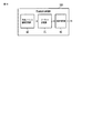
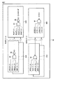
図4は、メモリセルアレイ内に設定されたセグメントに対応させて、不良セルを救済するための制御回路200を示している。本実施形態においては、図4に示される制御回路のことを、不良救済制御回路200と呼ぶ。不良救済制御回路200は、例えば、図1に示されるメモリセルアレイ1A〜1D及び冗長セルアレイ4などと同じチップ内に設けられる。
FIG. 4 shows a
不良救済制御回路200は、例えば、不良アドレス情報記憶部60、アドレス比較部70及び救済判定部80とを備える。不良制御回路200は、不良セルが接続されたワード線のアドレスが入力されたとき、ワード線と冗長ワード線との置き換えを制御する。
The defect
不良アドレス情報記憶部60は、不良セルを含むワード線(ロウ)及びセグメント(カラム)のアドレス情報を記憶している。以下、本実施形態における不良セルのアドレス情報のことを、不良アドレス情報と呼ぶ。不良アドレス情報記憶部60は、不良アドレス情報を記憶するため、例えば、フューズやROM(Read Only Memory)を有する。尚、本実施形態においては、不揮発性の抵抗変化型記憶素子を用いているので、不良アドレス情報は、メモリセルアレイと同一構成の記憶領域に記憶されてもよい。
The defective address
アドレス比較部70は、不良アドレス情報記憶部60から読み出された不良アドレス情報が、チップ内に入力されたアドレス情報(以下、選択アドレス情報と呼ぶ)と一致するか否かを比較する。尚、本実施形態においては、選択アドレス情報のうち、ロウを示すアドレス情報のことを、選択ロウアドレス情報とよび、カラムを示すアドレス情報のことを、選択カラムアドレス情報と呼ぶ。
The
救済判定部80は、不良アドレス情報と選択アドレス情報との比較結果を用いて、不良セルの救済(ワード線の置換)を行うか否かを判定する。
このような構成によって、不良救済制御回路200は、不良セルを含む1本のワード線において、不良セルが存在しているセグメントのワード線の部分を救済の単位として、不良セルを含むワード線の部分と冗長ワード線の部分との置き換えを、制御する。
The
With such a configuration, the defect
図5乃至図7を用いて、不良救済制御回路200の内部構成の一例について説明する。
An example of the internal configuration of the defect
図5は、不良アドレス情報記憶部60の内部構成の一例を示している。チップを構成しているメモリセルアレイ内のワード線のアドレス情報が11ビットで示される場合、11個の不良アドレス情報記憶部60が、1ビット分のロウアドレス情報にそれぞれ対応するように、設けられる。入力されたロウアドレス情報は、各ビットの桁に対応するように、各記憶部60のそれぞれに対して、1ビット分ずつ入力される。つまり、11個の不良アドレス情報記憶部60が1つの組となって、1本の不良セルを含むワード線のアドレス情報が示される。例えば、あるチップの不良セルの救済自由度が16のとき、16組の不良アドレス情報記憶部群が搭載される。
FIG. 5 shows an example of the internal configuration of the defective address
図5に示す例において、不良アドレス情報記憶部60は、例えば、レーザ溶断されるフューズ62A,62Bを利用して、メモリセルアレイの不良アドレス情報を記憶する。
In the example illustrated in FIG. 5, the defective address
1つの不良アドレス情報記憶部60は、2つのフューズ62A,62Bとそのフューズ62A,62Bが示す不良アドレス情報の読み出しを制御する回路群とを有している。
One defective address
不良セルが接続されたワード線のアドレス情報は、フューズ62A,62Bをレーザなどで溶断することによって、不良アドレス情報記憶部60内に、記憶される。
The address information of the word line to which the defective cell is connected is stored in the defective address
例えば、不良セルのロウアドレス情報が、“0”の場合、フューズ62A,62Bは溶断されない。これに対して、不良セルのロウアドレス情報(以下、不良ロウアドレス情報と呼ぶ)が、“1”の場合、フューズ62A,62Bは溶断される。つまり、不良ロウアドレス情報の各ビットが全て“0”である場合は、各不良アドレス情報記憶部60のフューズの溶断は不要である。これに対して、不良ロウアドレス情報の各ビットが全て“1”である場合、各不良アドレス情報記憶部60のフューズは、全て溶断される。
For example, when the row address information of the defective cell is “0”, the
本実施形態においては、図5に示すように、1ビット(“0”、“1”)分のロウアドレス情報に対して、つまり、1つの不良アドレス情報記憶部60内に対して、2つのフューズ62A,62Bが設けられている。これは、図1に示したように、1ビット分のカラムアドレス情報CAnに基づいて、2つのセグメント10A,11Aが1つのメモリセルアレイ1Aに対して設定された場合に、相当する。例えば、フューズ62Aは、“0”のカラムアドレス情報CAnに対応し、フューズ62Bは、“1”のカラムアドレス情報CAnに対応する。
この場合、1つの不良アドレス記憶部60に記憶される不良アドレス情報が、“1”のロウアドレス情報と“0”のカラムアドレス情報とを示すとき、フューズ62Aが溶断される。また、不良アドレス情報が、“1”のロウアドレス情報と“1”のカラムアドレス情報とを示すとき、フューズ62Bが溶断される。尚、不良アドレス情報が“0”のロウアドレス情報を示す場合、“0”及び“1”のカラムアドレス情報CAnに対応するフューズ62A,62Bのいずれも溶断されない。
In the present embodiment, as shown in FIG. 5, two row address information for one bit (“0”, “1”), that is, two in one defective address
In this case, when the defective address information stored in one defective
各フューズ62A,62Bは、CMOSインバータ61A,61Bの接地端子Vss側に接続される。
Each
各CMOSインバータ61A,61Bは、1つのP型MIS(Metal- Insulator- Semiconductor)トランジスタと1つのN型MISトランジスタとから構成されている。
P型MISトランジスタPT61A,PT61BのゲートとN型MISトランジスタNT61A,NT61Bのゲートとが、並列に接続され、入力ノードを成している。
Each
The gates of the P-type MIS transistors PT61A and PT61B and the gates of the N-type MIS transistors NT61A and NT61B are connected in parallel to form an input node.
P型MISトランジスタPT61A,PT61Bの電流経路の一端は、電源端子Vddに接続される。P型MISトランジスタPT61A,PT61Bの電流経路の他端は、N型MISトランジスタNT61A,NT61Bの電流経路の一端に接続されている。P型MISトランジスタPT61A,PT61BとN型MISトランジスタNT61A,NT61Bとの接続点が、出力ノードna,nbとなる。N型MISトランジスタNT61A,NT61Bの電流経路の他端は、フューズ62A,62Bの一端に接続される。そして、フューズ62A,62Bの他端が、接地端子Vssに接続されている。
フューズ62A,62Bが溶断されているとき、出力ノードna,nbは、電源電位Vdd1,Vdd2程度まで充電され、“H(high)”レベルを示す。
One end of the current path of the P-type MIS transistors PT61A and PT61B is connected to the power supply terminal Vdd. The other ends of the current paths of the P-type MIS transistors PT61A and PT61B are connected to one end of the current path of the N-type MIS transistors NT61A and NT61B. Connection points between the P-type MIS transistors PT61A and PT61B and the N-type MIS transistors NT61A and NT61B are output nodes na and nb. The other ends of the current paths of N-type MIS transistors NT61A and NT61B are connected to one ends of
When the
フューズ62A,62Bが溶断されていないとき、電源電位Vdd1,Vdd2はフューズ62A,62Bを経由して、接地電位Vss1,Vss2に放出されるため、出力ノードna,nbは“L(low)”レベルを示す。
When the
2つのCMOSインバータ61A,61Bの入力ノードには、チップ起動信号PWRONが、共通に入力される。
CMOSインバータ61Aの出力ノードnaは、ラッチ回路63Aの入力ノードに接続される。また、CMOSインバータの出力ノードnbは、ラッチ回路63Bの入力ノードに接続される。
The chip activation signal PWRON is commonly input to the input nodes of the two
The output node na of the
ラッチ回路63A,63Bのそれぞれは、例えば、2つのインバータ(NOTゲート)IV1a,IV2a,IV1b,IV2bから構成されている。ラッチ回路63A,63Bの出力ノードna’,nb’は、CMOSインバータ61A,61Bの出力ノードna,nbにおける信号の反転信号を保持する。
ラッチ回路63A,63Bの出力ノードna’,nb’は、クロックドインバータCIA,CIBの入力ノードにそれぞれ接続される。
Each of the
Output nodes na ′ and nb ′ of
クロックドインバータCIA,CIBは、2つのフューズ62A,62Bのそれぞれに対応して、設けられている。クロックドインバータCIA,CIBは、カラムアドレス信号CAnを、制御信号とする。そして、アクセスの対象となるメモリセルの1ビット分のカラムアドレス情報CAnに基づいて、2つのクロックドインバータCIA,CIBのうち、いずれか一方が活性化される。これによって、いずれか一方のフューズの状態に対応する信号が、選択的に出力される。
Clocked inverters CIA and CIB are provided corresponding to the two
各クロックドインバータCIA,CIBは、2つのPチャネル型MISトランジスタPT66A,PT66B,PT67A,PT67Bと2つのNチャネル型MISトランジスタNT66A,NT66B,NT67A,NT67Bとから構成されている。 Each clocked inverter CIA, CIB includes two P-channel MIS transistors PT66A, PT66B, PT67A, PT67B and two N-channel MIS transistors NT66A, NT66B, NT67A, NT67B.
フューズ62Aに対応するクロックドインバータCIAにおいて、P型MISトランジスタPT66AとN型MISトランジスタNT66Aとが、CMOSインバータを成している。そして、このCMOSインバータに対して、P型MISトランジスタPT66B及びN型MISトランジスタNT66Bは、トランスファーゲートとして機能する。
In the clocked inverter CIA corresponding to the
P型MISトランジスタPT66Aと電源端子Vdd3との間に、P型MISトランジスタPT66Bが設けられている。そのP型MISトランジスタPT66Bの電流経路の一端が、電源端子Vdd3に接続され、そのP型MISトランジスタPT66Bの電流経路の他端が、P型MISトランジスタPT66Aの電流経路の一端に直列に接続されている。
また、N型MISトランジスタNT66Aと接地端子Vss3との間に、N型MISトランジスタNT66Bが設けられている。そのN型MISトランジスタNT66Bの電流経路の一端が、接地端子Vss3に接続され、そのN型MISトランジスタNT66Bの電流経路の他端が、N型MISトランジスタNT66Aの電流経路の一端に直列に接続されている。
A P-type MIS transistor PT66B is provided between the P-type MIS transistor PT66A and the power supply terminal Vdd3. One end of the current path of the P-type MIS transistor PT66B is connected to the power supply terminal Vdd3, and the other end of the current path of the P-type MIS transistor PT66B is connected in series to one end of the current path of the P-type MIS transistor PT66A. Yes.
An N-type MIS transistor NT66B is provided between the N-type MIS transistor NT66A and the ground terminal Vss3. One end of the current path of the N-type MIS transistor NT66B is connected to the ground terminal Vss3, and the other end of the current path of the N-type MIS transistor NT66B is connected in series to one end of the current path of the N-type MIS transistor NT66A. Yes.
フューズ62Bに対応するクロックドインバータCIBは、クロックドインバータCIAとほぼ同様の構成によって、2つのP型MISトランジスタPT67A、PT67Bと2つのN型MISトランジスタNT67A,67Bとが、接続されている。
つまり、P型MISトランジスタPT67AとN型MISトランジスタNT67Aとが、CMOSインバータをなしている。そして、CMOSインバータをなすP型MISトランジスタPT67Aと電源端子Vdd4との間に、トランスファーゲートとして機能するP型MISトランジスタPT67Bが接続されている。また、CMOSインバータをなすN型MISトランジスタNT67Aと接地端子Vss4との間に、トランスファーゲートとして機能するN型MISトランジスタNT67Bが接続されている。
The clocked inverter CIB corresponding to the
That is, the P-type MIS transistor PT67A and the N-type MIS transistor NT67A form a CMOS inverter. A P-type MIS transistor PT67B functioning as a transfer gate is connected between the P-type MIS transistor PT67A forming the CMOS inverter and the power supply terminal Vdd4. Further, an N-type MIS transistor NT67B functioning as a transfer gate is connected between an N-type MIS transistor NT67A forming a CMOS inverter and the ground terminal Vss4.
ここで、2つのクロックドインバータCIA,CIBにおいて、トランスファーゲートとして機能するMISトランジスタPT66B,NT66B,PT67B,NT67Bのゲートに、カラムアドレス情報CAnが入力される。このカラムアドレス情報CAnの信号レベル(“L(0)”,“H(1)”)に応じて、クロックドインバータCIA,CIBのいずれか一方が選択的に活性化されるように、それらの動作が制御される。具体的には、以下のとおりである。 Here, in the two clocked inverters CIA and CIB, the column address information CAn is input to the gates of the MIS transistors PT66B, NT66B, PT67B, and NT67B that function as transfer gates. Depending on the signal level (“L (0)”, “H (1)”) of the column address information CAn, either one of the clocked inverters CIA and CIB is selectively activated. Operation is controlled. Specifically, it is as follows.
フューズ62Aに対応するクロックドインバータCIAにおいて、P型MISトランジスタPT66Bのゲートには、カラムアドレス情報CAnの同相信号が入力され、N型MISトランジスタNT66Bのゲートには、インバータ(NOTゲート)64Aを介して、カラムアドレス情報CAnの反転信号が入力される。
一方、フューズ62Bに対応するクロックドインバータCIBにおいて、P型MISトランジスタPT67Bのゲートには、インバータ(NOTゲート)64Aを介して、カラムアドレス情報CAnの反転信号が入力され、N型MISトランジスタNT67Bのゲートには、カラムアドレス情報CAnの同相信号が入力される。
In the clocked inverter CIA corresponding to the
On the other hand, in the clocked inverter CIB corresponding to the
カラムアドレス情報CAnが“0”(=“L”レベル)のとき、クロックドインバータCIAのトランスファーゲートとしてのトランジスタPT66B,NT66Bがオンになる。よって、クロックドインバータCIAはオンになり、入力された信号が転送可能となる。一方、クロックドインバータCIBにおいて、トランスファーゲートとしてのトランジスタPT67B,NT67Bはオフになるので、クロックドインバータCIBは信号を出力しない。
また、カラムアドレス情報CAnが“1”(=“H”レベル)のとき、クロックドインバータCIBのトランスファーゲートとしてのトランジスタPT67B,NT67Bがオンになる。よって、クロックドインバータCIBはオンになり、入力された信号が転送可能となる。一方、クロックドインバータCIAにおいて、トランスファーゲートとしてのトランジスタPT67B,NT67Bはオフになるので、クロックドインバータCIAは信号を出力しない。
When the column address information CAn is “0” (= “L” level), the transistors PT66B and NT66B as the transfer gates of the clocked inverter CIA are turned on. Therefore, the clocked inverter CIA is turned on, and the input signal can be transferred. On the other hand, in the clocked inverter CIB, the transistors PT67B and NT67B as transfer gates are turned off, so that the clocked inverter CIB does not output a signal.
When the column address information CAn is “1” (= “H” level), the transistors PT67B and NT67B as the transfer gates of the clocked inverter CIB are turned on. Therefore, the clocked inverter CIB is turned on, and the input signal can be transferred. On the other hand, in the clocked inverter CIA, the transistors PT67B and NT67B as transfer gates are turned off, so that the clocked inverter CIA does not output a signal.
これによって、2つのフューズ62A,62Bに記憶された不良アドレス情報は、カラムアドレス情報CAnの論理状態(“0”又は“1”)に基づいて動作する2つのクロックドインバータCIA,CIBによって、いずれか一方のクロックドインバータCIA,CIBの出力ノードnc,ndからノードne,nfへ出力される。このように、カラムアドレス情報CAnの論理状態を利用して、不良セルの存在するセグメントの情報を反映させ、不良セルを含むワード線のアドレス情報を読み出すことができる。
As a result, the defective address information stored in the two
また、不良セルの救済を考慮して、入力されたアドレス情報に対応したメモリセルにアクセスするために、入力されたアドレス情報と不良アドレス情報との比較が必要となる。このため、ノードne及びノードnfに出力された信号(1ビット分の不良アドレス情報)は、クロックドインバータCIC及びスイッチSWによって、アクセスの対象となるメモリセル(ワード線)のロウアドレス情報RA<0>と組み合わされて、記憶部出力信号FA<0>として、回路60外部へ出力される。尚、入力されたロウアドレス情報が含む全ビットのうち、各桁に対応する1ビット分のロウアドレス情報が、記憶部60のそれぞれに入力される。図4において、ロウアドレス情報RA<0>は、ロウアドレス情報の最下位の1ビット分(“0”又は“1”)を示している。
In consideration of repairing a defective cell, in order to access a memory cell corresponding to the input address information, it is necessary to compare the input address information with the defective address information. For this reason, the signal (defective address information for 1 bit) output to the node ne and the node nf is supplied by the clocked inverter CIC and the switch SW to the row address information RA <of the memory cell (word line) to be accessed. 0> and output to the outside of the
クロックドインバータCICは、CMOSインバータをなすP型及びN型MISトランジスタPT68A,NT68Aと、トランスファーゲートとして機能するP型及びN型MISトランジスタPT68B,PT68Bとから構成されている。P型MISトランジスタPT68Bの電流経路の一端は、電源端子Vdd5に接続され、P型MISトランジスタPT68Bの電流経路の他端は、P型MISトランジスタPT68Aの電流経路の一端に接続される。N型MISトランジスタNT68Bの電流経路の一端は、接地端子Vss5に接続され、N型MISトランジスタNT68Bの電流経路の他端は、N型MISトランジスタNT68Aの電流経路の一端に接続される。 The clocked inverter CIC includes P-type and N-type MIS transistors PT68A and NT68A forming a CMOS inverter, and P-type and N-type MIS transistors PT68B and PT68B functioning as transfer gates. One end of the current path of the P-type MIS transistor PT68B is connected to the power supply terminal Vdd5, and the other end of the current path of the P-type MIS transistor PT68B is connected to one end of the current path of the P-type MIS transistor PT68A. One end of the current path of the N-type MIS transistor NT68B is connected to the ground terminal Vss5, and the other end of the current path of the N-type MIS transistor NT68B is connected to one end of the current path of the N-type MIS transistor NT68A.
スイッチSWは、1つのP型MISトランジスタPT69と1つのN型MISトランジスタNT69とから構成されている。P型MISトランジスタPT69の電流経路の一端とN型MISトランジスタNT69の電流経路の一端が接続され、その接続された接点がスイッチSWの入力ノードをなしている。また、P型MISトランジスタPT69の電流経路の他端とN型MISトランジスタNT69の電流経路の他端が接続され、スイッチSWの出力ノードをなしている。 The switch SW is composed of one P-type MIS transistor PT69 and one N-type MIS transistor NT69. One end of the current path of the P-type MIS transistor PT69 and one end of the current path of the N-type MIS transistor NT69 are connected, and the connected contact forms an input node of the switch SW. Further, the other end of the current path of the P-type MIS transistor PT69 and the other end of the current path of the N-type MIS transistor NT69 are connected to form an output node of the switch SW.
クロックドインバータCICに対して、ノードneに出力された信号は、トランスファーゲートとしてのP型MISトランジスタPT68Bのゲートに入力され、ノードnfに出力された信号は、トランスファーゲートとしてのN型MISトランジスタNT68Bのゲートに入力される。 For clocked inverter CIC, the signal output to node ne is input to the gate of P-type MIS transistor PT68B as a transfer gate, and the signal output to node nf is N-type MIS transistor NT68B as a transfer gate. Input to the gate.
また、スイッチSWに対して、ノードneに出力された信号は、N型MISトランジスタNT69のゲートに入力され、ノードnfに出力された信号は、P型MISトランジスタPT69のゲートに入力される。 For the switch SW, the signal output to the node ne is input to the gate of the N-type MIS transistor NT69, and the signal output to the node nf is input to the gate of the P-type MIS transistor PT69.
ノードneには、インバータ64Bが接続されている。
An
ロウアドレス情報RA<0>は、CMOSインバータPT68A,NT68Aの入力ノードに入力される。また、ロウアドレス情報RA<0>は、スイッチSWの入力ノードに入力される。 Row address information RA <0> is input to the input nodes of CMOS inverters PT68A and NT68A. The row address information RA <0> is input to the input node of the switch SW.
フューズ62A,62Bが溶断されていない場合、つまり、ノードna,nbに出力される信号レベルが“L”レベルの場合、ノードneの信号レベルはインバータ64Bによって“H”レベルになる。その一方で、ノードnfの信号レベルは、“L”レベルになる。
この場合、トランスファーゲートとしてのP型MISトランジスタPT68Bは、ノードneからの信号(“H”レベル)によって、オフになり、トランスファーゲートとしてのN型MISトランジスタNT68Bは、ノードnfからの信号(“L”レベル)によって、オフになる。よって、クロックドインバータCICはオフになっている。
When fuses 62A and 62B are not blown, that is, when the signal level output to nodes na and nb is "L" level, the signal level of node ne is set to "H" level by
In this case, the P-type MIS transistor PT68B as a transfer gate is turned off by a signal (“H” level) from the node ne, and the N-type MIS transistor NT68B as a transfer gate is turned off by a signal (“L”). "Level" turns off. Therefore, the clocked inverter CIC is turned off.
このとき、スイッチSWにおいて、それを構成しているP型トランジスタPT69は、ノードnfからの信号(“L”レベル)によって、オンになり、それを構成しているN型トランジスタNT69は、ノードneからの信号(“H”レベル)を受けて、オンになる。よって、スイッチSWは、オンになる。
したがって、スイッチSWの出力信号が、記憶部出力信号FA<0>として、記憶部60の外部へ出力される。出力される記憶部出力信号FA<0>は、ロウアドレス情報RA<0>と同相の信号となる。
At this time, in the switch SW, the P-type transistor PT69 constituting the switch SW is turned on by a signal (“L” level) from the node nf, and the N-type transistor NT69 constituting the switch SW is turned on by the node ne. Is turned on in response to a signal ("H" level) from. Therefore, the switch SW is turned on.
Therefore, the output signal of the switch SW is output to the outside of the
フューズ62A,62Bが溶断されている場合、つまり、ノードna,nbに出力される信号が“H”レベルの場合、ノードneの信号レベルは“L”レベルになり、ノードnfの信号レベルは、インバータ64Bによって“H”レベルになる。それゆえ、クロックドインバータCIC及びスイッチSWの動作は、フューズ62A,62Bが溶断されていない場合と反対の動作になる。
つまり、トランスファーゲートとしてのP型MISトランジスタPT68Bは、ノードneからの信号(“L”レベル)によって、オンになり、トランスファーゲートとしてのN型MISトランジスタNT68Bは、ノードnfからの信号(“H”レベル)によって、オンになる。よって、クロックドインバータCICは、オンになり、入力ノードに入力された信号RA<0>をその出力ノードへ転送することが可能になる。
これに対し、スイッチSWにおいて、P型トランジスタPT69は、ノードnfからの信号(“H”レベル)によってオフになり、N型トランジスタNT69は、ノードneからの信号(“L”レベル)によってオフになる。よって、スイッチSWは、オフになる。
When the
That is, the P-type MIS transistor PT68B as a transfer gate is turned on by a signal (“L” level) from the node ne, and the N-type MIS transistor NT68B as a transfer gate is turned on by a signal (“H”). Level). Therefore, clocked inverter CIC is turned on, and signal RA <0> input to the input node can be transferred to the output node.
On the other hand, in switch SW, P-type transistor PT69 is turned off by a signal ("H" level) from node nf, and N-type transistor NT69 is turned off by a signal ("L" level) from node ne. Become. Therefore, the switch SW is turned off.
したがって、選択ロウアドレス情報RA<0>がクロックドインバータCICを経由して記憶部60の外部へ出力されるので、記憶部出力信号FA<0>は、選択ロウアドレス情報RA<0>が反転した信号となる。
Therefore, since the selected row address information RA <0> is output to the outside of the
よって、フューズ62A,62Bが溶断されていない場合、ロウアドレス情報RA<0>が“0”であれば、記憶部出力信号FA<0>は“0”(“L”レベル)を示し、ロウアドレス情報RA<0>が“1”であれば、記憶部出力信号FA<0>は“1”(“H”レベル)を示す。
また、フューズ62A,62Bが溶断されている場合、ロウアドレス情報RA<0>が“0”であれば、記憶部出力信号FA<0>は“1”(“H”レベル)を示し、ロウアドレス情報RA<0>が“1”であれば、記憶部出力信号FA<0>は“0”(“L”レベル)を示す。
Therefore, when the
When the
上述のように、フューズ62A,62Bの溶断は、“1”のロウアドレス情報に対応し、フューズ62A,62Bの不溶断は、“0”のロウアドレス情報に対応する。よって、読み出されたフューズ62A,62Bの状態(溶断/不溶断)に対応する信号レベルと入力されたロウアドレス情報RA<0>の信号レベルが一致した場合に、記憶部出力信号FA<0>は、“0”(“L”レベル)を示す。
As described above, the fusing of the
尚、不良アドレス情報記憶部60は、半導体メモリのロウアドレス情報のビット数に対応した個数、チップ内に設けられる。それゆえ、選択アドレス情報が含むロウアドレス情報が11ビットで示されているとき、各ビットの桁に対応して、1ビット分の記憶部出力信号FA<0>,FA<1>,・・・,FA<10>が、11個の不良アドレス情報記憶部60からそれぞれ出力される。以下、これらの複数の記憶部出力信号FA<0>,FA<1>,・・・,FA<10>を、“FA<0:10>”とも表記する。
The number of defective address
尚、図2に示すように、各メモリセルアレイ1A〜1Dが4つのセグメントに分割される場合には、2ビット分のカラムアドレス情報CAn,CA(n−1)に対応するように、4つのフューズと、それらのフューズの制御回路として、ラッチ回路やクロックドインバータが、記憶部60内に設けられる。そして、4つのフューズの状態と入力されたロウアドレス情報に対応して、1つの記憶部出力信号FA<0>が出力される。
以上のように、図5に示される不良アドレス記憶部60によって、カラムアドレス情報CAnを用いて設定されたセグメント単位で、不良セルのアドレスの判定及び不良セルの救済の制御が可能になる。
As shown in FIG. 2, when each of the
As described above, the defective
図6は、アドレス比較部70の回路構成の一例を示している。
アドレス比較部70は、不良セルの救済自由度に相当する個数、チップ内に設けられる。つまり、救済自由度が16のとき、アドレス比較部70の個数は、16個設けられる。そして、1つのアドレス比較部70が、1組の不良アドレス記憶部群に対して、それぞれ対応している
1つのアドレス比較部70には、1組の不良アドレス情報記憶部群60がそれぞれ出力した記憶部出力信号FA<0:10>が入力される。アドレス比較部70は、外部から入力されたアドレス情報と記憶部出力信号FA<0:10>とが一致するか否かを検出する。
FIG. 6 shows an example of the circuit configuration of the
The number of
図6に示されるアドレス比較部70は、入力された記憶部出力信号FA<0:10>が全て“L(0)”レベルになる場合に、不良セルの救済を要求する。尚、記憶部出力信号FA<0:10>が全て“L”になるのは、フューズの状態(溶断/不溶断)に対応する不良アドレス情報の全ビットと入力されたロウアドレス情報の全ビットとが一致した場合である。
The
アドレス比較部70は、その入力初段に、4つの3入力NORゲート71a〜71dを有する。3つのNORゲート71a〜71dの各入力端子に、不良アドレス情報記憶部60から出力された記憶部出力信号FA<0:8>が、それぞれ入力される。そして、残りの1つのNORゲート71dの3つの入力端子のうち、2つの入力端子に、2つの記憶部出力信号FA<9>,FA<10>がそれぞれ入力され、残りの1つの入力端子には、アドレス比較活性信号FRMが入力される。“L(0)”レベルのアドレス比較活性信号FAMが入力されると、記憶部出力信号FA<0:10>の論理状態(“0”又は“1”)に基づいた不良アドレス情報とロウアドレス情報との一致又は不一致の判定が、開始される。
The
各NORゲート71a〜71dの出力端子は、1つの4入力NANDゲート72の4つの入力端子にそれぞれ接続される。NANDゲート72の出力端子は、N型MISトランジスタ73のゲートに接続される。
N型MISトランジスタNT73の電流経路の一端には、P型MISトランジスタPT74の電流経路の一端が接続され、それらの電流経路の接続点は出力ノードngになっている。P型MISトランジスタPT74の電流経路の他端は、電源端子Vdd6に接続される。
The output terminals of the NOR
One end of the current path of the N-type MIS transistor NT73 is connected to one end of the current path of the P-type MIS transistor PT74, and the connection point of these current paths is the output node ng. The other end of the current path of the P-type MIS transistor PT74 is connected to the power supply terminal Vdd6.
N型MISトランジスタNT73の電流経路の他端には、N型MISトランジスタNT74の電流経路の一端が接続されている。N型MISトランジスタNT74の電流経路の他端には、接地端子Vss6に接続されている。
P型MISトランジスタPT74とN型トランジスタNT74のゲートには、チップ活性化信号ACTが入力される。チップ活性化信号ACTは、データの書き込み又は読み出しを指示するアクセスコマンドがチップに入力されると、“L”レベルから“H”レベルに遷移する。チップ活性化信号ACTが“L”レベルから“H”レベルに遷移する期間、ノードngには、オン状態のP型MISトランジスタPT74の電流経路を経由して、電源電位Vdd6が供給される。これによって、ノードngは、電源電位Vdd6程度に充電される。
One end of the current path of the N-type MIS transistor NT74 is connected to the other end of the current path of the N-type MIS transistor NT73. The other end of the current path of the N-type MIS transistor NT74 is connected to the ground terminal Vss6.
Chip activation signal ACT is input to the gates of P-type MIS transistor PT74 and N-type transistor NT74. The chip activation signal ACT transitions from the “L” level to the “H” level when an access command for instructing data writing or reading is input to the chip. During the period when the chip activation signal ACT transitions from the “L” level to the “H” level, the power supply potential Vdd6 is supplied to the node ng via the current path of the P-type MIS transistor PT74 in the on state. Thereby, node ng is charged to about power supply potential Vdd6.
N型MISトランジスタNT73とP型MISトランジスタPT74との出力ノードは、インバータ(NOTゲート)76Aの入力端子に接続される。
このインバータ76Aに対して、P型MISトランジスタPT75が並列に接続されている。P型MISトランジスタPT75のゲートは、インバータ76Aの出力端子に接続される。P型MISトランジスタPT75の電流経路の一端は、インバータ76Aの入力端子に接続され、P型MISトランジスタPT75の電流経路の他端は、電源端子Vdd6に接続される。このP型MISトランジスタPT75は、チップ活性化信号ACTを制御信号とするP型MISトランジスタPT74の動作を補償するために設けられ、出力ノードngがフローティング状態になるのを防ぐ。
Output nodes of N-type MIS transistor NT73 and P-type MIS transistor PT74 are connected to an input terminal of inverter (NOT gate) 76A.
A P-type MIS transistor PT75 is connected in parallel to the
インバータ76Aの出力端子に、インバータ76Bの入力端子が接続されている。これによって、インバータ76Bの出力信号は、出力ノードngから出力された信号と同相の信号になる。
The input terminal of the inverter 76B is connected to the output terminal of the
インバータ76Bの出力端子は、インバータ77の入力端子に接続される。
The output terminal of the inverter 76B is connected to the input terminal of the
インバータ77は、入力された信号を反転し、その信号を比較信号RMH<0>として、後述の救済判定部80に出力する。
The
記憶部出力信号FA<0:10>が全て“L(0)”レベルのとき、“L”レベルの出力信号が、N型MISトランジスタNT73のゲートに入力され、N型MISトランジスタNT73はオフになる。よって、ノードngの充電状態は保持され、ノードngの信号レベルは“H”レベルを示す。 When the memory unit output signals FA <0:10> are all at the “L (0)” level, the “L” level output signal is input to the gate of the N-type MIS transistor NT73, and the N-type MIS transistor NT73 is turned off. Become. Therefore, the charged state of the node ng is maintained, and the signal level of the node ng indicates the “H” level.
それゆえ、記憶部出力信号FA<0:10>が全て“L”レベルの場合、比較信号RMH<0>は、“L(0)”レベルを示す。すなわち、比較信号RMH<0>は、不良アドレス情報が選択ロウアドレス情報と一致した場合に対応して、“L”レベルになる。 Therefore, when all the storage unit output signals FA <0:10> are at the “L” level, the comparison signal RMH <0> indicates the “L (0)” level. That is, the comparison signal RMH <0> is set to the “L” level corresponding to the case where the defective address information matches the selected row address information.
記憶部出力信号FA<0:10>のいずれか1つが“H”レベルのとき、“H”レベルの出力信号が、N型MISトランジスタNT73のゲートに入力され、N型MISトランジスタNT73はオンになる。また、N型MISトランジスタNT74は、チップ活性化信号ACTの“L”レベルから“H”レベルへの遷移によって、オンになっている。出力ノードngに充電された電位(電荷)は、オンになっているN型MISトランジスタNT73,NT74の電流経路を経由して、接地端子Vss6に放出される。よって、ノードngの信号レベルは“L”レベルになる。
それゆえ、記憶部出力信号FA<0:10>のいずれか1つ以上が“H”レベルの場合、比較信号RMH<0>は、“H(0)”レベルを示す。すなわち、“H”レベルの比較信号RMH<0>は、不良アドレス情報が選択ロウアドレス情報と一致しない場合に対応する。このように、比較信号RMH<0>は、チップ活性化信号ACTが“L”レベルから“H”レベルに遷移するのと同期して、“H”レベルになる。
When any one of the storage unit output signals FA <0:10> is at “H” level, an “H” level output signal is input to the gate of the N-type MIS transistor NT73, and the N-type MIS transistor NT73 is turned on. Become. The N-type MIS transistor NT74 is turned on by the transition of the chip activation signal ACT from the “L” level to the “H” level. The potential (charge) charged in the output node ng is discharged to the ground terminal Vss6 via the current path of the N-type MIS transistors NT73 and NT74 that are turned on. Therefore, the signal level of the node ng becomes “L” level.
Therefore, when any one or more of the storage unit output signals FA <0:10> is at the “H” level, the comparison signal RMH <0> indicates the “H (0)” level. That is, the “H” level comparison signal RMH <0> corresponds to the case where the defective address information does not match the selected row address information. As described above, the comparison signal RMH <0> becomes “H” level in synchronization with the transition of the chip activation signal ACT from “L” level to “H” level.
インバータ76Bの出力端子は、2入力NANDゲート78の入力端子の一方に接続される。このNANDゲート78の入力端子の他方には、隣接して配置されている他のアドレス比較部からの比較信号RMH<1>が入力される。
NANDゲート78は、インバータ76B(ノードng)からの出力信号と比較信号RMH<1>との演算結果を、インバータ79を経由して、一致信号SDE<0>として、救済判定部80へ出力する。
The output terminal of the inverter 76B is connected to one of the input terminals of the 2-
The
アドレス比較部70が出力する一致信号SRDE<0>は、記憶部出力信号FA<0>と入力されたロウアドレス情報とが一致した状態を示す。この一致信号SDRE<0>が“L”レベルから“H”レベルに遷移した場合に、不良セルのロウ救済が要求される。“L”レベルの一致信号SDRE<0>は、その信号を出力したアドレス比較部70に対応する冗長ワード線を用いての救済は実行されないことに対応する。
The coincidence signal SRDE <0> output from the
一致信号SDRE<0>を“L”レベルから“H”レベルを遷移させるのは、隣接して配置された比較部70からの比較信号RMH<1>が“L”レベルから“H”レベルへ遷移するのを利用して実現できる。これは、2つの比較信号RMH<0>,RMH<1>が同時に“L”レベル(一致状態)にならない、つまり、1つアクセスサイクルで1つのメモリセル(不良セル)を2つの冗長セルで救済することはありえないためである。
The coincidence signal SDRE <0> is changed from the “L” level to the “H” level because the comparison signal RMH <1> from the
図6に示されるアドレス比較回路70の説明から明らかなように、不良セルのアドレス情報が“0”の場合、不良アドレス記憶部60内のフューズ62A,62Bを溶断せず、不良セルのアドレス情報が“1”の場合、不良アドレス記憶部60内フューズ62A,62Bを溶断しておくことによって、アドレス比較部70は、不良セルのアドレス情報と入力された選択アドレス情報とが一致するか否かを検出できる。
As is apparent from the description of the
図7は、救済判定部80の回路構成の一例を示している。
図7に示される救済判定部80は、アドレス比較部70から出力された複数の情報を統合して、アクセス対象のメモリセル(ワード線)を活性化するか非活性化するかを、最終的に判定する。図7の救済判定部80には、16個のアドレス比較部70の出力信号RMH<0:15>,SRDE<0:15>が入力される。尚、アドレス比較部70の個数は、チップの救済自由度の数に相当するため、図7に示される救済判定部80は、救済自由度が16の場合に用いる回路構成になっている。
FIG. 7 shows an example of the circuit configuration of the
The
この場合、救済判定部80を構成する演算部81A,81B,86A,86Bは、16個の比較信号RMH<0:15>と16個の一致信号SRDE<0:15>とを、演算する。ここで、比較信号RMH<0:15>は、比較信号RMH<0>,RMH<1>,・・・,RMH<14>,RMH<15>を示している。また、一致信号SRDE<0:15>も、比較信号RMH<0:15>と同様である。
In this case, the
救済判定部80において、16個の比較信号RMH<0:15>は、演算部81A,81Bによって、演算される。
16個の比較信号RMH<0:15>は、演算部81Aに入力される。1つの演算部81Aは、1つの4入力NANDゲート82と、その出力端子に接続されるインバータ(NOTゲート)83とから構成される。本例においては、16個の比較信号RMH<0:15>に対して、4つの演算部81Aが、救済判定部80内に設けられる。比較信号RMH<0:15>のそれぞれは、NANDゲートの入力端子のそれぞれに入力される。図7においては、図示の簡単化のため、1つの演算部81Aの内部構成を図示し、1つの端子にそれぞれ入力される比較信号を、RMH<0:3>、RMH<4:7>、RMH<8:11>、RMH<12:15>と図示している。
In the
The 16 comparison signals RMH <0:15> are input to the
4つの比較信号が、1つのNANDゲート82によって論理演算される。
1つのNANDゲート82による演算結果は、インバータ(NOTゲート)83を経由して、出力信号RMHIT<0>として出力される。よって、4つの演算部81Aによって、4つの出力信号RMHIT<0:3>が出力される。
Four comparison signals are logically operated by one
A calculation result by one
出力信号RMHIT<0:3>は、演算部81Bに入力される。この演算部81Bは、1つの4入力NANDゲート84と1つのインバータ(NOTゲート)85とから構成されている。4つの出力信号RMHIT<0:3>は、NANADゲート84によって、論理演算される。
The output signal RMHIT <0: 3> is input to the
NANDゲート84による演算結果は、インバータ85を経由して、出力信号XMISSHITとして、救済判定部80の外部へ出力される。
The calculation result by the NAND gate 84 is output to the outside of the
本例において、出力信号XMISSHITは、比較信号RMH<0:15>が全て“H”レベルの場合に、“H”レベルを示す。この“H”レベルの出力信号XMISSHITは、不良アドレス情報と選択ロウアドレス情報とが一致しない場合に対応している。
このように、冗長セルを使用しない場合、つまり、チップ内に入力されたアドレス情報に対して、不良セルの救済が必要ない場合に、出力信号XMISSHITは“H”レベルを示す。
In this example, the output signal XMISSHIT indicates the “H” level when all the comparison signals RMH <0:15> are at the “H” level. This “H” level output signal XMISSHIT corresponds to the case where the defective address information does not match the selected row address information.
As described above, when the redundant cell is not used, that is, when the defective cell need not be relieved with respect to the address information input in the chip, the output signal XMISSHIT indicates the “H” level.
これによって、出力信号XMISSHITが“H”レベルの場合、入力されたアドレス情報が示すメモリセルアレイ内のワード線が活性化され、そのワード線に接続されたメモリセルがアクセスの対象となる。尚、不良セルの救済が実行される場合には、出力信号XMISSHITは“L”レベルを示す。 Thus, when the output signal XMISSHIT is at “H” level, the word line in the memory cell array indicated by the input address information is activated, and the memory cell connected to the word line becomes the access target. Note that when the repair of the defective cell is executed, the output signal XMISSHIT indicates the “L” level.
救済判定部80において、一致信号SRDE<0:15>は、演算部86A,86Bによって、演算される。
16個の一致信号SRDE<0:15>は、演算部81Aに入力される。1つの演算部81Aは、1つの4入力NORゲート87から構成される。この場合、16個の一致信号SRDE<0:15>に対して、4つの演算部81Aが、救済判定部80内に設けられる。
In the
The 16 match signals SRDE <0:15> are input to the
一致信号SRDE<0:15>のそれぞれは、NORゲート87の入力端子のそれぞれに入力される。尚、図7においては、図示の簡単化のため、1つの演算部86Aの内部構成を図示し、1つの端子にそれぞれ入力される一致信号を、SRDE<0:3>、SRDE<4:7>、SRDE<8:11>、SRDE<12:15>と図示している。
NORゲート87による演算結果は、出力信号bSRDE<0:3>として、出力される。4つの出力信号RMHIT<0:3>が、4つの演算部86Aから演算部86Bに出力される。
Each of the coincidence signals SRDE <0:15> is input to each of the input terminals of the NOR
The calculation result by the NOR
出力信号bSRDE<0:3>は、演算部86Bに入力される。この演算部86Bは、1つの4入力NANDゲート84から構成されている。4つの出力信号bSRDE<0:3>は、NANADゲート84によって、論理演算される。 The output signal bSRDE <0: 3> is input to the calculation unit 86B. The arithmetic unit 86B is composed of one 4-input NAND gate 84. The four output signals bSRDE <0: 3> are logically operated by the NANAD gate 84.
NANDゲート84による演算結果は、出力信号XHITとして、救済判定部80の外部へ出力される。
The calculation result by the NAND gate 84 is output to the outside of the
本例において、出力信号XHITは、複数の一致信号RMH<0:15>のうち、少なくとも1つが“H(1)”レベルの場合に、“H(1)”レベルを示す。この“H”レベルの出力信号XHITは、不良アドレス情報と入力されたアドレス情報とが一致した場合に対応している。
このように、冗長セルを使用する場合、つまり、チップ内の不良セルの救済が必要な場合に、出力信号XHITは“H”レベルを示す。
これによって、出力信号XHITが“H”レベルの場合、冗長セルアレイ内のある冗長ワード線が活性化され、その冗長ワード線に接続された冗長セルがアクセスの対象となる。尚、不良セルの救済がない場合には、出力信号XHITは“L”レベルを示す。
In this example, the output signal XHIT indicates the “H (1)” level when at least one of the plurality of coincidence signals RMH <0:15> is at the “H (1)” level. This "H" level output signal XHIT corresponds to the case where the defective address information matches the input address information.
As described above, when the redundant cell is used, that is, when it is necessary to repair the defective cell in the chip, the output signal XHIT indicates the “H” level.
As a result, when the output signal XHIT is at “H” level, a certain redundant word line in the redundant cell array is activated, and the redundant cell connected to the redundant word line becomes an access target. When there is no repair of the defective cell, the output signal XHIT indicates “L” level.
以上のように図7に示される救済判定部80が出力する信号XMISSHITは、比較信号RMH<0:15>のNAND論理の演算結果を示す。また、救済判定部80が出力する信号XHITは、一致信号SRDE<0:15>のOR論理の演算結果を示す。
これによって、入力されたロウアドレス情報が、複数の不良アドレス情報の全てと一致しなければ、不良セルの救済は行われないように、制御される。また、入力されたロウアドレス情報が、複数の不良アドレス情報のうちいずれか1つと一致していれば、カラムアドレス情報と組み合わせたロウ救済法によって、不良セルが救済されるように、ワード線及び冗長ワード線の動作が、ロウデコーダによって制御される。
As described above, the signal XMISSHIT output from the
As a result, if the input row address information does not match all of the plurality of pieces of defective address information, control is performed so that defective cells are not relieved. In addition, if the input row address information matches any one of the plurality of defective address information, the word line and the word line and the row line are repaired by the row repair method combined with the column address information. The operation of the redundant word line is controlled by the row decoder.
以上の構成によって、本発明の第1の実施形態の抵抗変化型不揮発性半導体メモリにおいて、カラムアドレ情報を組み合わせて、不良セルが接続されたワード線の一部分と冗長ワード線の一部分とを置き換え、不良セルを救済できる。 With the above configuration, in the variable resistance nonvolatile semiconductor memory according to the first embodiment of the present invention, the column address information is combined to replace a part of the word line connected to the defective cell and a part of the redundant word line. The cell can be rescued.
(b) 動作
以下、図8を用いて、本発明の第1の実施形態に係る不揮発性半導体メモリの動作について、説明する。尚、ここでは、図8と共に、図1乃至図7に示される等価回路図を用いて、説明する。
(B) Operation
Hereinafter, the operation of the nonvolatile semiconductor memory according to the first embodiment of the present invention will be described with reference to FIG. Here, description will be made using the equivalent circuit diagrams shown in FIGS. 1 to 7 together with FIG.
図1乃至図7に示された回路を有するメモリチップにおいて、そのメモリチップの製造後に、テスト工程が実行され、メモリセルアレイ1A〜1D内の不良セルが検知される。本実施形態においては、不良セルのアドレス情報が、図4に示される不良セル情報記憶部60内のフューズ62A,62Bに記憶される。また、不良セル(ワード線)と冗長セル(冗長ワード線)との対応関係も、あらかじめ設定される。
In the memory chip having the circuits shown in FIGS. 1 to 7, a test process is performed after the memory chip is manufactured, and defective cells in the
図8に示されるように、メモリチップに、電源電位Vddが投入される。電源電位Vddを投入した初期段階においては、チップ起動信号であるパワーオン信号PWRONは、“L”レベルを示す。 As shown in FIG. 8, the power supply potential Vdd is input to the memory chip. In the initial stage when the power supply potential Vdd is turned on, the power-on signal PWRON that is the chip activation signal indicates the “L” level.
そして、電源電位Vddが、チップを駆動できる所定の電位に達すると、チップ起動信号PWRONが“L”レベルから“H”レベルへ遷移する。
図4に示される不良アドレス情報記憶部60内において、チップ起動信号PWRONの信号レベルが“L”レベルから“H”レベルへ遷移している間、フューズ62A,62Bが溶断されている場合、ノードna,nbは、電源電位Vdd1,Vdd2によって、充電される。よって、CMOSインバータの出力ノードna,nbの信号レベルは、“H”レベルを示す。一方、フューズ62A,62Bが溶断されていない場合、ノードna,nbに供給された電位は、そのフューズ62A,62Bを経由して、接地電位Vssへ放出される。よって、インバータの出力ノードna,nbの信号レベルは、“L”レベルを示す。
When the power supply potential Vdd reaches a predetermined potential at which the chip can be driven, the chip activation signal PWRON changes from the “L” level to the “H” level.
In the defective address
そして、チップの動作時、ノードna,nbの信号(“H”又は“L”レベル)は、ラッチ回路63A,63Bの出力ノードna’,nb’において、ノードna,nbの反転信号として保持される。このように、チップの動作時、ノードna’,nb’にラッチされた状態が不良セルのアドレス情報を読み出すための初期状態となって、そのフューズの溶断/不溶断を示す情報が保持される。
During the operation of the chip, the signals (“H” or “L” level) of the nodes na and nb are held as inverted signals of the nodes na and nb at the output nodes na ′ and nb ′ of the
次に、書き込み動作又は読み出し動作がチップに対して指示された時、そのアクセスの対象となるメモリセルの位置を示すアドレス情報(選択アドレス情報)が、チップ内に入力される。この選択アドレス情報は、ワード線(ロウ)を示すロウアドレス情報とビット線(カラム)を示すカラムアドレス情報とを含んでいる。 Next, when a write operation or a read operation is instructed to the chip, address information (selected address information) indicating the position of the memory cell to be accessed is input into the chip. This selection address information includes row address information indicating a word line (row) and column address information indicating a bit line (column).
本実施形態において、1ビット分のカラムアドレス情報CAn(“0(L)”又は“1(H)”)により、フューズ62A,62Bに対応したいずれか一方のクロックドインバータCIA,CIBが、オンになる。そして、ノードna’あるいはノードnb’にそれぞれ保持されている信号(“H”または“L”)のいずれか一方が、オンになった一方のクロックドインバータの出力ノードnc,ndに出力される。
カラムアドレス情報CAn=“0”(=“L”レベル)の場合、ノードna’(na)の情報(信号)がノードncに転送される。これに対して、カラムアドレス情報CAn=“1”(=“H”レベル)の場合、ノードnb’(nb)の情報(信号)がノードndに転送される。このように、本実施形態においては、ロウ救済式における不良アドレス情報の読み出しに対して、不良セルのカラムアドレス情報CAnが反映される。
転送されたノードna’,nb’の信号は、オンになっているクロックドインバータCIA,CIBによって反転されて出力される。よって、出力ノードnc,ndの信号レベルは、ノードna,nbにおける信号レベルと同相になっている。
In the present embodiment, one of the clocked inverters CIA and CIB corresponding to the
When the column address information CAn = “0” (= “L” level), the information (signal) of the node na ′ (na) is transferred to the node nc. On the other hand, when the column address information CAn = “1” (= “H” level), the information (signal) of the node nb ′ (nb) is transferred to the node nd. As described above, in this embodiment, the column address information CAn of the defective cell is reflected in reading the defective address information in the row relief method.
The transferred signals at the nodes na ′ and nb ′ are inverted and output by the clocked inverters CIA and CIB that are turned on. Therefore, the signal levels at the output nodes nc and nd are in phase with the signal levels at the nodes na and nb.
出力ノードnc,ndに転送された信号は、ノードne,nfに出力される。ノードneに出力された信号の信号レベルは、インバータ64によって、出力ノードnc,ndにおける信号レベルと反対にされる。ノードnfに出力された信号の信号レベルは、出力ノードnc,ndにおける信号レベルと同じになっている。 The signals transferred to the output nodes nc and nd are output to the nodes ne and nf. The signal level of the signal output to the node ne is reversed by the inverter 64 from the signal level at the output nodes nc and nd. The signal level of the signal output to node nf is the same as the signal level at output nodes nc and nd.
フューズ62A,62Bが溶断されていない場合、つまり、出力ノードnc,ndから出力される信号のレベルが“L”レベルの場合、トランスファーゲートとしてのトランジスタPT68B,NT68Bはオフになり、クロックドインバータCICがオフになる。一方、スイッチSWを構成する2つのトランジスタPT69,NT69はオンになる。 When fuses 62A and 62B are not blown, that is, when the level of a signal output from output nodes nc and nd is “L” level, transistors PT68B and NT68B as transfer gates are turned off, and clocked inverter CIC Turns off. On the other hand, the two transistors PT69 and NT69 constituting the switch SW are turned on.
よって、ロウアドレス情報RA<0>がスイッチSWを経由して出力されるので、図8に示すように、記憶部出力信号FA<0>はロウアドレス情報RA<0>と同相の信号を示す。つまり、フューズ62A,62Bが溶断されていない場合、ロウアドレス情報RA<0>が“0”のとき、記憶部出力信号FA<0>は“0”(“L”レベル)を示し、ロウアドレス情報RA<0>が“1”のとき、記憶部出力信号FA<0>は“1”(“H”レベル)を示す。
Therefore, since the row address information RA <0> is output via the switch SW, the storage unit output signal FA <0> indicates a signal in phase with the row address information RA <0> as shown in FIG. . That is, when the
フューズ62A,62Bが溶断されている場合、つまり、出力ノードnc,ndから出力される信号のレベルが“H”レベルの場合、クロックドインバータCICはオン(転送可能状態)になり、スイッチSWはオフになる。よって、ロウアドレス情報RA<0>がクロックドインバータCICを経由して出力されるので、記憶部出力信号FA<0>はロウアドレス情報RA<0>の反転信号を示す。つまり、フューズ62A,62Bが溶断されている場合、ロウアドレス情報RA<0>が“0”のとき、記憶部出力信号FA<0>は“1”(“H”レベル)を示し、ロウアドレス情報RA<0>が“1”のとき、記憶部出力信号FA<0>は“0”(“L”レベル)を示す。
上述のように、フューズ62A,62Bが溶断されていないのは、ロウアドレス情報RA<0>が“0”であることに対応し、フューズ62A,62Bが溶断されているのは、ロウアドレス情報RA<0>が“1”であることに対応する。よって、読み出されたフューズ62A,62Bの状態(溶断/不溶断)が示す信号(不良ロウアドレス情報)と入力されたロウアドレス情報RA<0>が一致した場合に、“0”レベルの記憶部出力信号FA<0>が出力される。
When fuses 62A and 62B are blown, that is, when the level of the signal output from output nodes nc and nd is “H” level, clocked inverter CIC is turned on (transferable state), and switch SW is Turn off. Accordingly, since the row address information RA <0> is output via the clocked inverter CIC, the storage unit output signal FA <0> indicates an inverted signal of the row address information RA <0>. That is, when the
As described above, the
このような動作が、ロウアドレス情報が11ビットである場合、11個の不良アドレス情報記憶部60によって、実行される。また、救済自由度に応じた個数の不良アドレス記憶部群で、同様の動作が実行される。
Such an operation is executed by the 11 defective address
以上のように、フューズの溶断の有無によって、不良セルのロウアドレス情報RA<0>(“0”又は“1”)が示される。また、カラムアドレス情報CAnに基づいて、複数(本例では、2つ)のフューズ62A,62Bのうち、いずれか1つのフューズの情報が、選択的に出力される。このため、不良セルが、ロウアドレス情報に対応したどのワード線に接続され、且つ、メモリセルアレイ内のカラムアドレス情報に対応したどこの領域に存在しているか、不良アドレス情報記憶部60の出力信号によって示される。
As described above, the row address information RA <0> (“0” or “1”) of the defective cell is indicated depending on whether or not the fuse is blown. Further, based on the column address information CAn, information on any one of the plurality of (two in this example) fuses 62A and 62B is selectively output. For this reason, the output signal of the defective address
図6に示すように、11個の不良アドレス情報記憶部60のそれぞれから出力された記憶部出力信号FA<0:10>は、1つのアドレス比較部70に入力される。
As shown in FIG. 6, storage unit output signals FA <0:10> output from each of the 11 defective address
11個の記憶部出力信号FA<0:10>は、4つの3端子NORゲート71a〜71dの入力端子にそれぞれ入力され、それらのNORゲート71a〜71dの入力端子の1つに、アドレス比較活性信号FRMが入力される。電源電圧がチップに投入されると、アドレス比較活性信号FRMは“H(1)”レベルから“L(0)”レベルへ遷移する。これに同期して、入力された記憶部出力信号FA<0:10>が一致するか否かの判定が開始される。
電源電圧がチップに投入された後、アクセスコマンドがチップに入力されると、チップ活性化信号ACTも、“L”レベルから“H”レベルへ遷移する。このチップ活性化信号ACTの信号レベルが遷移する期間において、ノードngの信号レベルは“L”レベルから“H”レベルに遷移する。
Eleven storage unit output signals FA <0:10> are input to the input terminals of four three-terminal NOR
When an access command is input to the chip after the power supply voltage is input to the chip, the chip activation signal ACT also changes from the “L” level to the “H” level. In the period in which the signal level of the chip activation signal ACT changes, the signal level of the node ng changes from “L” level to “H” level.
上述のように、複数の不良アドレス記憶部60のそれぞれにおいて、読み出されたフューズ62A,62Bの状態(溶断/不溶断)が示す信号と入力されたロウアドレス情報RA<0:10>が一致した場合に、記憶部出力信号FA<0:10>は、全て“0”(“L”レベル)になる。
As described above, in each of the plurality of defective
複数の記憶部出力信号FA<0:10>が全て“0(L)”であるとともに、アドレス比較活性信号FRMが“0”であるとき、各NORゲート71a〜71dから演算結果“1(H)”が、NANDゲート72に出力される。この結果として、NANDゲート72は、“0(L)”の信号を、N型MISトランジスタNT73のゲートに出力する。これによって、N型MISトランジスタNT73はオフになり、ノードngが示す信号レベルは“H(1)”レベルに保持される。
When the plurality of storage unit output signals FA <0:10> are all “0 (L)” and the address comparison activation signal FRM is “0”, the calculation result “1 (H) from each NOR
複数の記憶部出力信号FA<0:10>が1つでも“1(H)”を含む場合、NORゲート71a〜71dのいずれか1つは“0”を出力する。このため、NANDゲート72の出力は、“1”(“H”レベル)になる。よって、N型MISトランジスタNT73は、オンになる。また、チップ活性信号ACTが“H”レベルであると、P型MISトランジスタPT74はオフになり、N型MISトランジスタNT74はオンになる。これによって、ノードngの電位は、接地端子Vss6と同じ電位になる。
したがって、記憶部出力信号FA<0:10>が“1”を含む場合、ノードngの信号レベルは、“L(0)”レベルになる。尚、アドレス比較活性信号FRMが“H(1)”レベルを示している間、NANDゲート72は、“0(L)”の信号を出力するため、N型MISトランジスタNT73はオフになっている。
When even one of the plurality of storage unit output signals FA <0:10> includes “1 (H)”, one of the NOR
Therefore, when the memory unit output signal FA <0:10> includes “1”, the signal level of the node ng becomes the “L (0)” level. Note that while the address comparison activation signal FRM indicates the “H (1)” level, the
ノードngの出力信号は、3つのインバータ76A,76B,77を経由して、比較信号RMH<0>として、判定部80に出力される。よって、ノードngの信号レベルが“L”レベルの場合、比較信号RMH<0>は、“H”レベルを示す。この“H”レベルの比較信号RMH<0>は、不良セルのロウアドレス情報と選択ロウアドレス情報とが不一致である場合に相当するので、不良セルの救済は要求されない。
一方、ノードngの信号レベルが“H”レベルの場合、比較信号RMH<0>は、“L”レベルを示す。“L”レベルの比較信号RMH<0>は、不良セルのアドレス情報と入力されたロウアドレス情報とが一致する場合に相当する。
The output signal of the node ng is output to the
On the other hand, when the signal level of the node ng is “H” level, the comparison signal RMH <0> indicates “L” level. The “L” level comparison signal RMH <0> corresponds to the case where the address information of the defective cell matches the input row address information.
ノードngの出力信号は、2つのインバータ76A,76Bを経由して、NANDゲート78に入力される。そして、NANDゲート78によって、ノードngの出力信号は、隣接するアドレス比較部からの比較信号RMH<1>と演算される。NANDゲート78による演算結果は、一致信号SRDE<0>として、インバータ79を経由し、判定部80に出力される。一致信号SRDE<0>が、“L(0)”レベルから“H(1)”レベルへ遷移する場合に、不良セルの救済が要求される。
The output signal of the node ng is input to the
以上のように、アドレス比較部70に入力された記憶部出力信号FA<0:10>が、全て“L”レベルを示す場合、それは、不良セルのロウアドレス情報と選択されたメモリセルのロウアドレス情報が一致する、つまり、不良セルが接続されたワード線が選択されたことを示す。それゆえ、比較信号RMH<0>が“L”レベル、一致信号SRDE<0>が“H”レベルとなり、不良セルの救済が実行される。
また、記憶部出力信号FA<0:10>が少なくとも1つ“H”レベルを含む場合、それは、不良セルが接続されたワード線は選択されていないことを意味し、比較信号RMH<0>が“H”レベルになるので、不良セルの救済は行われない。
As described above, when all of the storage unit output signals FA <0:10> input to the
Further, when the storage unit output signal FA <0:10> includes at least one “H” level, it means that the word line to which the defective cell is connected is not selected, and the comparison signal RMH <0>. Since it becomes “H” level, the defective cell is not relieved.
不良セルの救済自由度が16の場合、16個のアドレス比較回路70がチップ内に設けられる。そして、上記のアドレス比較部70の動作によって、アドレス比較回路70のそれぞれから、比較信号RMH<0:15>及び一致信号SEDE<0:15>が、図7に示される判定回路70に出力される。
When the degree of freedom for repairing a defective cell is 16, 16
16個の比較信号RMH<0:15>は、判定回路80内の演算部81A,81Bによって、演算される。16個の比較信号RMH<0:15>は、演算部81A,81Bによって、NAND論理が演算される。
よって、入力された比較信号RMH<0:15>が全て“H(1)”レベルのとき、つまり、16個の不良アドレス情報の全てと入力されたロウアドレス情報とが一致しなかったとき、出力信号XMISSHITは、“H(1)”レベルを示す。“H(1)”レベルの出力信号XMISSHITが出力された場合、不良セルの救済は実行されない。
The 16 comparison signals RMH <0:15> are calculated by the
Therefore, when all the input comparison signals RMH <0:15> are at the “H (1)” level, that is, when all the 16 pieces of defective address information do not match the input row address information, The output signal XMISSHIT indicates the “H (1)” level. When the output signal XMISSHIT of “H (1)” level is output, the defective cell is not relieved.
一方、16個の一致信号SRDE<0:15>は、判定回路80内の演算部81A,81Bによって、演算される。16個の一致信号SRDE<0:15>は、演算部81A,81Bによって、OR論理が演算される。
よって、入力された一致信号SRDE<0:15>のうち、いずれか1つが“H(1)”レベルのとき、つまり、記憶された複数の不良アドレス情報のうち、1つの不良アドレス情報と入力されたロウアドレス情報とが一致した場合、出力信号XHITは、“H(1)”レベルを示す。“H(1)”レベルの出力信号XHITが出力された場合、不良セルの救済が実行される。
On the other hand, the 16 match signals SRDE <0:15> are calculated by the
Therefore, when any one of the input coincidence signals SRDE <0:15> is at the “H (1)” level, that is, one piece of defective address information and input among a plurality of pieces of stored defective address information. When the row address information matches, the output signal XHIT indicates the “H (1)” level. When the output signal XHIT of “H (1)” level is output, the defective cell is repaired.
この動作によって、不良セルを救済すると判定された場合、入力されたロウアドレス情報が示すワード線の代わりに、冗長ワード線が活性化される。そして、活性化された冗長ワード線に接続された複数の冗長セルおいて、不良セルと同じ1ビット分のカラムアドレス情報(セグメント)に対応した冗長セルに対して、データの書き込み又はデータの読み出しが実行される。 By this operation, when it is determined to repair the defective cell, the redundant word line is activated instead of the word line indicated by the input row address information. In a plurality of redundant cells connected to the activated redundant word line, data is written to or read from the redundant cell corresponding to the same 1-bit column address information (segment) as the defective cell. Is executed.
以上のように、複数の不良アドレス情報記憶部60において、フューズの溶断の有無によって、不良アドレス情報(ワード線のアドレス)が記憶される。各不良アドレス情報記憶部のフューズの数は、カラムアドレス情報に基づくメモリセルアレイのセグメントと同じ数、設けられている。そして、カラムアドレス情報に基づいて、2以上のフューズのうち、いずれか1つのフューズの情報が出力される。このように、不良アドレス情報は、不良アドレス情報記憶部60内に、カラムアドレス情報CAnを対応させた領域(セグメント)毎に記憶され、入力されたカラムアドレス情報に基づいて、個別に読み出される。
これによって、本実施形態のように、ロウ救済方式を採用した場合において、不良セルがメモリセルアレイ内のどこカラムに存在するか、換言すると、1つのワード線のどこの部分に接続されているかを特定することができる。
As described above, in the plurality of defective address
As a result, when the row relief method is employed as in this embodiment, it is possible to determine in which column in the memory cell array the defective cell exists, in other words, to which part of one word line is connected. Can be identified.
そして、カラムアドレス情報を対応させた不良をドレス情報に基づいて、アドレス比較部70及び判定部80によって、不良セルの救済が必要か否か、判定される。
Then, based on the dress information, the defect that corresponds to the column address information is determined by the
よって、メモリセルアレイ内に、カラムアドレス情報に基づいた2つ以上のセグメントを設定することによって、セグメントに対応したワード線の一部分を、救済単位として、ワード線の不良セルが接続された一部分と冗長ワード線の一部分とを置換できる。
尚、不良セルが接続されたワード線において、そのワード線の不良セルが存在しないセグメント内のメモリセルがアクセスの対象となった場合、そのワード線が活性化され、通常通りに、そのワード線に接続されたメモリセルが用いられる。
Therefore, by setting two or more segments based on the column address information in the memory cell array, a part of the word line corresponding to the segment is used as a repair unit and a part connected to the defective cell of the word line is redundant. A part of the word line can be replaced.
When a memory cell in a segment where a defective cell of the word line does not exist is accessed in the word line to which the defective cell is connected, the word line is activated and the word line is activated as usual. A memory cell connected to is used.
例えば、本実施形態の抵抗変化型不揮発性半導体メモリが、ランダムアクセスメモリである場合には、上記の動作が、書き込み/読み出しのためのアドレス情報が入力されるたびに、随時実行される。 For example, when the variable resistance nonvolatile semiconductor memory according to the present embodiment is a random access memory, the above operation is performed whenever the address information for writing / reading is input.
以上のように、ワード線をカラムアドレス情報に基づいて論理的に分割して制御することで、冗長ワード線の本数の増加及び冗長セルアレイの占有面積の増大を伴わないで、救済できる不良セルの個数を増加できる。 As described above, the word lines are logically divided and controlled based on the column address information, so that the number of redundant word lines and the area occupied by the redundant cell array can be saved without increasing the number of redundant cell lines. The number can be increased.
したがって、本発明の第1の実施形態の抵抗変化型不揮発性半導体メモリによれば、不良セルの救済効率を向上できる。 Therefore, according to the variable resistance nonvolatile semiconductor memory of the first embodiment of the present invention, the repair efficiency of defective cells can be improved.
[第2の実施形態]
図9及び図10を用いて、本発明の第2の実施形態について、説明する。尚、図9及び図10において、第1の実施形態と実質的に同じ構成要素については、同じ符号を付し、詳細な説明は必要に応じて行う。
[Second Embodiment]
A second embodiment of the present invention will be described with reference to FIGS. 9 and 10. In FIGS. 9 and 10, substantially the same components as those in the first embodiment are denoted by the same reference numerals, and detailed description will be given as necessary.
図9は、階層ワード線方式と呼ばれるワード線の構成を有する半導体メモリのメモリセルアレイ近傍の回路構成を示している。 FIG. 9 shows a circuit configuration in the vicinity of a memory cell array of a semiconductor memory having a word line configuration called a hierarchical word line system.
図9に示す階層ワード線方式のメモリセルアレイ9A〜9Dにおいて、ワード線の構成は、2つの階層を有している。そのため、本実施形態のワード線は、メインワード線MWLとメインワード線MWLに接続されるサブワード線SWLとから構成される。
In the hierarchical word line type
1つのメモリセルアレイ9A〜9Dは、物理的に分割されている複数の領域90A〜90D,91A〜91Dから構成されている。本実施形態において、物理的に分割されている領域90A〜90D,91A〜91Dのことを、ブロック90A〜90D,91A〜91Dと呼ぶ。
One
図9に示す例においては、メモリセルアレイ9A〜9Dのそれぞれは、2つのブロック90A〜90D,91A〜91Dを有している。1つのメモリセルアレイ9A〜9Dにおいて、2つのブロック90A〜90D,91A〜91Dは、X方向に並んで配置されている。
In the example shown in FIG. 9, each of the
各メモリセルアレイ9A〜9D内に、複数のメインワード線MWLが設けられている。メインワード線MWLは、例えば、Y方向に延在し、X方向に並んで配置されている。複数のメインワード線MWLは、Y方向に隣接している2つのブロック90A〜90D,91A〜91Dに跨っている。
複数のサブワード線SWLは、ブロック90A〜90D,91A〜91D毎に、設けられている。複数のサブワード線SWLは、1つのメインワード線MWLに対して、共通に接続されている。サブワード線SWLは、Y方向に延在し、X方向に並んで配置される。
A plurality of main word lines MWL are provided in each of the
The plurality of sub word lines SWL are provided for each of the
メインロウデコーダ20Aは、1つのメモリセルアレイ9A〜9Dに対して、1つ設けられ、メインワード線MWLを共有する複数のブロック90A〜90D,91A〜90Dによって共通に用いられる。メインロウデコーダ20Aは、入力されたロウアドレス情報に基づいて、メインワード線MWLの活性化及び非活性化を制御する。
One
サブロウデコーダ21A〜21D,22A〜22Dは、ブロック90A〜90D,91A〜91DのY方向に隣接して設けられている。サブロウデコーダ21A〜21D,22A〜22Dは、各ブロック90A〜90D,91A〜91Dに対して、1つずつ設けられる。そして、サブロウデコーダ21A〜21D,22A〜22Dは、サブワード線SWLの活性化及び非活性化を制御する。
The
複数の冗長セルを備える冗長セルアレイ100は、メモリセルアレイ9A〜9Dと同様に、階層ワード線方式が採用されている。1つの冗長セルアレイ100は、物理的に分割されている2つの冗長ブロック101,102から構成されている。
As with the
複数の冗長メインワード線RMWLは、Y方向に隣接する2つの冗長ブロック101,102に跨って、配設される。冗長メインワード線RMWLは、Y方向に延在し、X方向に並んで配置されている。複数の冗長サブワード線RSWLは、冗長ブロック101,102毎に、設けられている。冗長サブワード線RSWLは、Y方向に延在し、X方向に並んで配置される。複数のサブワード線RSWLが、1つの冗長メインワード線RMWLに対して、共通に接続されている。 The plurality of redundant main word lines RMWL are arranged across two redundant blocks 101 and 102 adjacent in the Y direction. Redundant main word line RMWL extends in the Y direction and is arranged side by side in the X direction. A plurality of redundant sub word lines RSWL are provided for each of the redundant blocks 101 and 102. Redundant sub word line RSWL extends in the Y direction and is arranged side by side in the X direction. A plurality of sub word lines RSWL are commonly connected to one redundant main word line RMWL.
冗長メインロウデコーダ50は、1つの冗長セルアレイ100に対して1つ設けられ、2つの冗長ブロック101,102に対して、共通に用いられる。冗長サブロウデコーダ51,52は、冗長ブロック101,102毎に、1つずつ設けられる。
One redundant
冗長メインワード線RMWLは、冗長メインロウデコーダ50によって、その活性化/非活性化が制御される。冗長サブワード線RSWLは、冗長サブロウデコーダ51,52によって、その活性化/非活性化が制御される。
Redundant main word line RMWL is controlled to be activated / deactivated by redundant
本実施形態のように、階層ワード線方式を採用することによって、メモリセルアレイの規模が増大することに伴って、ワード線長が増大した場合、その配線長の増大に起因する配線遅延の増大や製造歩留まりの低下を抑制できる。 As in this embodiment, when the word line length increases with the increase in the size of the memory cell array by adopting the hierarchical word line system, the increase in wiring delay due to the increase in the wiring length A decrease in manufacturing yield can be suppressed.
図10は、階層ワード線方式を採用した場合における、ロウデコーダ20A,21A,22Aの内部構成の一例を示している。
図10に示される例では、1本のメインワード線MWLは、2つのブロック90A,91Aに跨って配設され、そのメインワード線MWLが、複数のサブワード線SWLによって共通に用いられる。サブワード線SWLは、各ブロック90A,91Aに対して、4本設けられている。尚、図10においては、説明の簡単化のため、1本のメインワード線のみを図示しているが、メモリセルアレイに対して、2本以上のメインワード線が配設されてもよいのは、もちろんである。これと同様に、サブワード線の本数及びメモリセルアレイの個数も、図10に示される数に限定されない。
FIG. 10 shows an example of the internal configuration of the
In the example shown in FIG. 10, one main word line MWL is disposed across two
メインロウデコーダ20Aは、例えば、NANDゲート2から構成される。メインワード線MWLは、NANDゲート2の出力端子に接続される。そして、NANDゲート2の入力端子には、ロウアドレス情報が入力される。ロウアドレス情報は、選択されたメインワード線のロウアドレス情報を示している。入力されたロウアドレス情報は、NANDゲート2により論理演算される。その演算結果に基づいて、メインワード線WMLの活性化/非活性化が制御される。
The
サブロウデコーダ21A,22A内には、複数のドライバユニット25が設けられている。1つのサブロウデコーダ21A,22A内に設けられるドライバユニットの個数は、1つのサブロウデコーダ21A,22A内に設けられる。サブワード線SWLの本数に対応している。1つのドライバユニット25は、1つのサブワード線SWLに接続されている。
A plurality of
また、サブロウデコーダ21A,22A内には、第1の駆動線WDRV<0:3>と第2の駆動線bWDRV<0:3>が設けられている。駆動線WDRV<0:3>,bWDRV<0:3>の本数は、各サブロウデコーダ21A,22A内に設けられたドライバユニットの個数及びサブワード線SWLの本数に対応している。図10に示す例において、4個のドライバユニットが設けられているので、4本の駆動線WDRV<0:3>と、4本の駆動線bWDRV<0:3>が設けられている。チップの駆動時において、第1の駆動線WDRV<0:3>と第2の駆動線bWDRV<0:3>は対をなして駆動され、互いに反対の信号レベルに設定される。
Further, the first drive lines WDRV <0: 3> and the second drive lines bWDRV <0: 3> are provided in the
各ドライバユニット25は、簡素な回路構成を有し、1つのP型MISトランジスタ28と2つのN型トランジスタ29a,29bとから構成されている。
Each
1つのサブロウデコーダ21A,22Aにおいて、各ドライバユニット25を構成するP型MISトランジスタ28の電流経路の一端は、それぞれ異なる駆動線WDRV<0:3>に接続されている。
P型MISトランジスタの電流経路の他端は、N型MISトランジスタ29a,29bの電流経路の一端に接続される。このP型MISトランジスタとN型MISトランジスタ29a,29bとの接続点(ノード)に、サブワード線SWLが接続される。
N型MISトランジスタ29a,29bの電流経路の他端は、接地端子に接続される。
In one
The other end of the current path of the P-type MIS transistor is connected to one end of the current path of the N-
The other ends of the current paths of the N-
P型MISトランジスタ28のゲートとN型MISトランジスタ29aのゲートは、メインワード線MWLに接続されている。
N型MISトランジスタ29bのゲートは、駆動線WDRV<0:3>に接続される。1つのサブロウデコーダ21A,22Aにおいて、各ドライバユニット25を構成するN型MISトランジスタ29bのゲートは、それぞれ異なる駆動線bWDRV<0:3>に接続されている。
サブロウデコーダ21A,22Aは、2つの駆動線WDRV<0:3>,bWDRV<0:3>の信号レベルを制御することによって、ドライバユニット25を駆動し、サブワード線SMLの活性化/非活性化を制御する。駆動線WDRV<0:3>,bWDRV<0:3>に入力される信号は、サブワード線のアドレス情報である。
The gate of the P-
The gate of N-
The
メモリセルMCは、サブワード線SWLのそれぞれに、複数個接続される。各メモリセルMCは、第1の実施形態と同様に、1つの抵抗変化型記憶素子MTJと1つの選択トランジスタTrとから構成されている。本実施形態においては、選択トランジスタTrのゲートは、サブワード線SWLに接続される。 A plurality of memory cells MC are connected to each of the sub word lines SWL. Each memory cell MC includes one resistance change type storage element MTJ and one selection transistor Tr, as in the first embodiment. In the present embodiment, the gate of the selection transistor Tr is connected to the sub word line SWL.
ワード線階層方式を用いたメモリセルアレイの動作は、以下のようになる。 The operation of the memory cell array using the word line hierarchical system is as follows.
メモリセルへアクセスするためのロウアドレス情報は、メインロウデコーダ20A内に、入力される。
Row address information for accessing the memory cell is input into the
メモリセルのロウアドレス情報は、メインロウデコーダ20A内のNANDゲート2によって、論理演算される。このNANDゲート2の演算結果に基づいて、メインロウデコーダ20Aは、メインワード線MWLを活性化又は非活性化する。
そして、活性化されたメインワード線MWLの信号レベルは、“H”レベルから“L”レベルへ遷移する。尚、非活性化されたメインワード線MWLの信号レベルは、“L”レベルを示す。
The row address information of the memory cell is logically operated by the
Then, the signal level of the activated main word line MWL changes from the “H” level to the “L” level. Note that the signal level of the deactivated main word line MWL indicates the “L” level.
この状態で、サブロウデコーダ21A,22A内に設けられた駆動線WDRV<0:3>,bWDRV<0:3>が、入力されたロウアドレス情報に基づいて、選択的に活性化される。
In this state, the drive lines WDRV <0: 3> and bWDRV <0: 3> provided in the
メインワード線MWLの信号レベルが“L”レベルになると、P型MISトランジスタ28はオンになり、一方のN型MISトランジスタ29aはオフになる。
When the signal level of the main word line MWL becomes “L” level, the P-
そして、駆動線bWDRV<0:3>の1つが“L”レベルに設定された場合、他方のN型MISトランジスタ29bはオフになる。“L”レベルに設定された駆動線bWDRV<0:3>と対をなす駆動線WDRV<0:3>は、“H”レベルに設定される。このため、P型MISトランジスタ29の電流経路とN型MISトランジスタの電流経路との接続点は、オン状態のP型MISトランジスタの電流経路を経由して、駆動線WDRV<0:3>の設定電位によって、充電される。
これによって、ロウアドレス情報が示すサブワード線SWLの信号レベルは“L”レベルから“H”レベルに遷移し、そのサブワード線SWLは活性化される。
When one of the drive lines bWDRV <0: 3> is set to the “L” level, the other N-
As a result, the signal level of the sub word line SWL indicated by the row address information changes from the “L” level to the “H” level, and the sub word line SWL is activated.
尚、選択されていない残りの駆動線bWDRV<0:3>は、“H”レベルに設定され、残りの駆動線WDRV<0:3>は、“L”レベルに設定される。それゆえ、選択されていないサブワード線SWLは活性化されない。 The remaining unselected drive lines bWDRV <0: 3> are set to the “H” level, and the remaining drive lines WDRV <0: 3> are set to the “L” level. Therefore, the non-selected sub word line SWL is not activated.
以上のように、メインワード線MWL及びサブワード線SWLに接続されたメモリセルに対して、アクセスが可能になる。これと同様の動作によって、冗長メインワード線RMWL及び冗長サブワード線RSWLに接続されたメモリセルに対して、アクセスが実行される。 As described above, it becomes possible to access the memory cells connected to the main word line MWL and the sub word line SWL. By an operation similar to this, access is executed to the memory cells connected to the redundant main word line RMWL and the redundant sub word line RSWL.
本発明の第2の実施形態においては、階層ワード線方式が採用された不揮発性半導体メモリに対して、メインワード線をロウ救済法の対象として、不良セルを救済する。
本実施形態においては、1つのメモリセルアレイ9A〜9Dを構成している複数の物理的な領域(ブロック)90A〜90Dに対して、カラムアドレス情報CAnが割り付けられる。
メモリセルへのアクセス時、不良セルを救済するか否かが、判定される。不良セルを救済する場合、1本のメインワード線MWLは、カラムアドレス情報CAnに基づいて、2つに分割されて制御される。そして、分割されたメインワード線MWLの部分毎に、それに対応する冗長メインワード線RMWLの部分と置き換えられる。
例えば、メモリセルアレイ9A内において、不良セルbMC1は、メインワード線MWLaに接続されたサブワード線SWLaに含まれている。不良セルbMC1は、カラムアドレス情報CAn=“0”に対応するブロック90Aに存在している。
また、メモリセルアレイ9C内において、不良セルbMC2は、メインワード線MWLcに接続されたサブワード線SWLcに含まれている。不良セルbMC2は、カラムアドレス情報CAn=“1”に対応するブロック91Cに存在している。
In the second embodiment of the present invention, a defective cell is relieved by using a main word line as a target of a row relieving method for a nonvolatile semiconductor memory adopting a hierarchical word line system.
In the present embodiment, column address information CAn is allocated to a plurality of physical areas (blocks) 90A to 90D constituting one
When accessing the memory cell, it is determined whether or not to repair the defective cell. In the case of repairing a defective cell, one main word line MWL is divided into two parts and controlled based on the column address information CAn. Then, each divided main word line MWL is replaced with a corresponding redundant main word line RMWL.
For example, in the
Further, in the
不良セルbMC1,bMC2の不良アドレス情報は、カラムアドレス情報CAnに対応させて、例えば、第1の実施形態で述べた図4乃至図7とほぼ同様な構成の回路60〜70を用いて、記憶され、チップ内に入力されたアドレス情報と一致するか否か判定される。
本実施形態においては、不良セルbMC1,bMC2を含むメインワード線MWLa,MWLcの一部分MWLa<0>,MWLc<1>は、不良セルが存在するブロックがカラムアドレス情報に基づいて判別されることによって、そのカラムアドレス情報(ブロック)に対応する1本の冗長メインワード線RMWLの部分RMWL<0>,RMWL<1>と、それぞれ置き換えられる。
The defective address information of the defective cells bMC 1 and bMC 2 is associated with the column address information CAn, for example, by using the
In this embodiment, the blocks MWLa <0> and MWLc <1> of the main word lines MWLa and MWLc including the defective cells bMC 1 and bMC 2 are determined based on the column address information. Thus, the parts RMWL <0> and RMWL <1> of one redundant main word line RMWL corresponding to the column address information (block) are respectively replaced.
不良アドレス情報と入力されたアドレス情報が一致した場合、上記のメインワード線の一部分と冗長メインワード線との置き換えにより、冗長メインワード線RMWLが活性化され、所定の冗長セルが利用される。よって、不良セルの救済が実行される。 When the defective address information matches the inputted address information, the redundant main word line RMWL is activated by replacing a part of the main word line with the redundant main word line, and a predetermined redundant cell is used. Therefore, repair of the defective cell is executed.
一方、メインワード線MWLaにおいて、カラムアドレス情報CAn=“1”に対応する部分MWLa<1>は、不良セルを含まない。よって、カラムアドレス情報CAn=“1”に対応するメインワード線MWLaの部分MWLa<1>に対して、アクセスが生じた場合、メインワード線MWLaの部分MWLa<1>は、メインロウデコーダ20Aによって、活性化され、通常どおりに、サブワード線SWLに接続されたメモリセルが用いられる。これと同様に、カラムアドレス情報CAn=“0”に対応するメインワード線MWLcの部分MWLc<0>は、アクセスの対象として用いられ、その部分MWLb<0>を示すアドレス情報が入力された場合、メインワード線MWLcは活性化される。
On the other hand, in the main word line MWLa, the part MWLa <1> corresponding to the column address information CAn = “1” does not include a defective cell. Therefore, when an access occurs to the part MWLa <1> of the main word line MWLa corresponding to the column address information CAn = “1”, the part MWLa <1> of the main word line MWLa is received by the
このように、本実施形態において、不良セルが救済される場合、2本のメインワード線MWLがそれぞれ含む一部分を、1本の冗長メインワード線RWMLを用いて、置き換えることができる。例えば、1本の冗長メインワード線RWLと1ビット分のカラムアドレス情報CAnとを用いた場合において、その救済自由度は2になる。
それゆえ、必要な冗長ワード線の本数、換言すると、冗長セル数の増加及び冗長セルアレイの占有面積の増加を伴わないで、救済できる不良セルの個数を増加できる。
As described above, in this embodiment, when a defective cell is relieved, a part of each of the two main word lines MWL can be replaced by using one redundant main word line RWML. For example, when one redundant main word line RWL and 1-bit column address information CAn are used, the degree of freedom of relief is 2.
Therefore, it is possible to increase the number of defective cells that can be remedied without increasing the number of necessary redundant word lines, in other words, without increasing the number of redundant cells and the occupied area of the redundant cell array.
したがって、第2の実施形態の階層ワード線方式を用いた不揮発性半導体メモリのように、1つのメモリセルアレイ内に設けられた複数の物理的な領域(ブロック)に対して、カラムアドレス情報を割り付けて、ワード線に接続された不良セルを救済する場合においても、第1の実施形態と同様に、不良セルの救済効率を向上できる。 Therefore, column address information is assigned to a plurality of physical areas (blocks) provided in one memory cell array, like the nonvolatile semiconductor memory using the hierarchical word line system of the second embodiment. Thus, even when a defective cell connected to the word line is remedied, the remedy efficiency of the defective cell can be improved as in the first embodiment.
3. その他
本発明の実施形態に係る抵抗変化型不揮発性半導体メモリにおいて、第1の実施形態と第2の実施形態を組み合わせた構成、すなわち、1つのブロック内にカラムアドレス情報に基づいた複数のセグメントを設定しても良いのはもちろんである。この場合においても、不良セルの救済効率を向上できる。
本発明の実施形態に係る抵抗変化型不揮発性半導体メモリは、例えば、ランダムアクセスメモリに適用される。
3. Other
In the variable resistance nonvolatile semiconductor memory according to the embodiment of the present invention, a configuration combining the first embodiment and the second embodiment, that is, setting a plurality of segments based on column address information in one block Of course, you can. Even in this case, the repair efficiency of defective cells can be improved.
The variable resistance nonvolatile semiconductor memory according to the embodiment of the present invention is applied to, for example, a random access memory.
本発明の例は、上述の実施形態に限定されるものではなく、その要旨を逸脱しない範囲で、各構成要素を変形して具体化できる。また、上述の実施形態に開示されている複数の構成要素の適宜な組み合せにより種々の発明を構成できる。例えば、上述の実施形態に開示される全構成要素から幾つかの構成要素を削除してもよいし、異なる実施形態の構成要素を適宜組み合わせてもよい。 The example of the present invention is not limited to the above-described embodiment, and can be embodied by modifying each component without departing from the scope of the invention. Various inventions can be configured by appropriately combining a plurality of constituent elements disclosed in the above-described embodiments. For example, some constituent elements may be deleted from all the constituent elements disclosed in the above-described embodiments, or constituent elements of different embodiments may be appropriately combined.
1A〜1D,9A〜9D:メモリセルアレイ、2A〜2D:ロウデコーダ、3:センスアンプ、4,100:冗長セルアレイ、5:冗長ロウデコーダ、10A〜10D,11A〜11D、40,41:セグメント、20A〜20D:メインロウデコーダ、21A〜21D,22A〜22D:スペアロウデコーダ、50:冗長メインロウデコーダ、51,52:冗長サブロウデコーダ、60:不良アドレス情報記憶部、70:アドレス比較部、80:救済判定部、90A〜90D,91A〜91D,110,111:ブロック、WL,WLa,WLb,WL0〜WLn−1:ワード線、BL,BL0〜BLm−1:ビット線、MWL,MWLa,MWLb:メインワード線、SWL,SWLa,SWLb:サブワード線、RWL:冗長ワード線、RMWL:冗長メインワード線、SRWL:冗長サブワード線、MC:メモリセル、MTJ:抵抗変化型記憶素子、Tr:選択トランジスタ。 1A to 1D, 9A to 9D: Memory cell array, 2A to 2D: Row decoder, 3: Sense amplifier, 4, 100: Redundant cell array, 5: Redundant row decoder, 10A to 10D, 11A to 11D, 40, 41: Segment, 20A to 20D: main row decoder, 21A to 21D, 22A to 22D: spare row decoder, 50: redundant main row decoder, 51, 52: redundant sub row decoder, 60: defective address information storage unit, 70: address comparison unit, 80 : rescue determination unit, 90A~90D, 91A~91D, 110,111: block, WL, WLa, WLb, WL 0 ~WL n-1: the word line, BL, BL 0 ~BL m- 1: bit line, MWL , MWLa, MWLb: main word line, SWL, SWLa, SWLb: sub-word line, RWL: redundant word Word lines, RMWL: redundant main word line, SRWL: redundant sub-word lines, MC: memory cells, MTJ: resistance variable memory element, Tr: selection transistor.
Claims (5)
前記複数のメモリセルが接続され、第1の方向に延在する複数のワード線と、
前記メモリセルアレイの近傍に配置され、前記ワード線を活性化するロウデコーダと、
前記メモリセルアレイ内に含まれる不良セルの代わりに用いられる複数の冗長セルが配置された冗長セルアレイと、
前記複数の冗長セルが接続され、前記第1の方向に延在する複数の冗長ワード線と、
前記冗長セルアレイの近傍に配置され、前記冗長ワード線を活性化する冗長ロウデコーダと、
不良セルが接続されたワード線を示す不良アドレス情報が記憶され、入力されたアドレス情報と前記不良アドレス情報とが一致した場合に、前記不良セルを救済する制御回路と、
を具備し、
前記メモリセルアレイ及び前記冗長セルアレイは、カラムアドレス情報に基づいて判別され、前記第1の方向に分割された少なくとも2つ以上の領域をそれぞれ含み、
前記制御回路は、前記領域毎に、前記不良セルが接続された前記ワード線の一部分と前記冗長ワード線の一部分とを置き換えて、その置き換えられた冗長ワード線を前記冗長ロウデコーダに活性化させる、ことを特徴とする抵抗変化型不揮発性半導体メモリ。 A memory cell array in which a plurality of memory cells including a resistance change type storage element are arranged in a matrix;
A plurality of word lines connected to the plurality of memory cells and extending in a first direction;
A row decoder disposed in the vicinity of the memory cell array and activating the word line;
A redundant cell array in which a plurality of redundant cells used in place of defective cells included in the memory cell array are disposed;
A plurality of redundant word lines connected to the plurality of redundant cells and extending in the first direction;
A redundant row decoder disposed in the vicinity of the redundant cell array and activating the redundant word line;
Control circuit for relieving the defective cell when the defective address information indicating the word line to which the defective cell is connected is stored and the input address information matches the defective address information;
Comprising
The memory cell array and the redundant cell array each include at least two regions that are determined based on column address information and are divided in the first direction,
The control circuit replaces a part of the word line to which the defective cell is connected and a part of the redundant word line for each region, and activates the replaced redundant word line in the redundant row decoder. A variable resistance nonvolatile semiconductor memory characterized by the above.
前記冗長ワード線は、前記複数の冗長セルが接続され、前記領域毎にそれぞれに設けられる複数の冗長サブワード線と、前記複数の冗長サブワード線が共通に接続され、前記2つ以上の領域に跨って配設される冗長メインワード線と、から構成され、
前記制御回路は、前記領域毎に、前記不良セルが接続された前記メインワード線の一部分と前記冗長メインワード線の一部分とを置き換える、ことを特徴とする請求項1に記載の抵抗変化型不揮発性半導体メモリ。 The word line is connected to the plurality of memory cells, and the plurality of sub word lines provided for each region and the plurality of sub word lines are connected in common, and are arranged across the two or more regions. A main word line, and
The redundant word line is connected to the plurality of redundant cells, and the plurality of redundant sub word lines provided in each region and the plurality of redundant sub word lines are connected in common and span the two or more regions. A redundant main word line, and
2. The variable resistance nonvolatile memory according to claim 1, wherein the control circuit replaces a part of the main word line to which the defective cell is connected and a part of the redundant main word line for each region. Semiconductor memory.
前記不良アドレス記憶部は、
前記不良アドレス情報が記憶され、前記カラムアドレス情報に基づいて判別される2つ以上の領域に対応してそれぞれ設けられる2つ以上の記憶素子と、
前記2つ以上の記憶素子にそれぞれ対応して設けられ、前記カラムアドレス情報に基づいて、前記記憶素子の1つから不良アドレス情報を選択的に読み出すスイッチ素子と、
を備えることを特徴とする請求項1乃至3のいずれか1項に記載の抵抗変化型不揮発性半導体メモリ。 The control circuit includes one or more defective address storage units that store the defective address information,
The defective address storage unit
Two or more storage elements respectively provided corresponding to two or more areas in which the defective address information is stored and determined based on the column address information;
A switch element provided corresponding to each of the two or more storage elements, and selectively reading out defective address information from one of the storage elements based on the column address information;
The variable resistance nonvolatile semiconductor memory according to claim 1, further comprising:
入力されたアドレス情報と前記不良アドレス情報とが一致するか否かを比較するアドレス比較部と、
前記アドレス比較部の比較結果に基づいて、不良セルを救済するか否かを判定する救済判定部と、を備えることを特徴とする請求項1乃至4のいずれか1項に記載の抵抗変化型不揮発性半導体メモリ。 The control circuit includes:
An address comparison unit for comparing whether the input address information matches the defective address information;
The resistance change type according to claim 1, further comprising: a repair determination unit that determines whether or not to repair a defective cell based on a comparison result of the address comparison unit. Non-volatile semiconductor memory.
Priority Applications (2)
| Application Number | Priority Date | Filing Date | Title |
|---|---|---|---|
| JP2008324322A JP2010146665A (en) | 2008-12-19 | 2008-12-19 | Resistance change type nonvolatile semiconductor memory |
| US12/563,559 US8254192B2 (en) | 2008-12-19 | 2009-09-21 | Resistance change memory |
Applications Claiming Priority (1)
| Application Number | Priority Date | Filing Date | Title |
|---|---|---|---|
| JP2008324322A JP2010146665A (en) | 2008-12-19 | 2008-12-19 | Resistance change type nonvolatile semiconductor memory |
Publications (1)
| Publication Number | Publication Date |
|---|---|
| JP2010146665A true JP2010146665A (en) | 2010-07-01 |
Family
ID=42265811
Family Applications (1)
| Application Number | Title | Priority Date | Filing Date |
|---|---|---|---|
| JP2008324322A Pending JP2010146665A (en) | 2008-12-19 | 2008-12-19 | Resistance change type nonvolatile semiconductor memory |
Country Status (2)
| Country | Link |
|---|---|
| US (1) | US8254192B2 (en) |
| JP (1) | JP2010146665A (en) |
Cited By (2)
| Publication number | Priority date | Publication date | Assignee | Title |
|---|---|---|---|---|
| US8942023B2 (en) | 2011-08-05 | 2015-01-27 | Renesas Electronics Corporation | Semiconductor device |
| US9786365B2 (en) | 2015-07-31 | 2017-10-10 | Kabushiki Kaisha Toshiba | Integrated circuit |
Families Citing this family (57)
| Publication number | Priority date | Publication date | Assignee | Title |
|---|---|---|---|---|
| US8139409B2 (en) | 2010-01-29 | 2012-03-20 | Unity Semiconductor Corporation | Access signal adjustment circuits and methods for memory cells in a cross-point array |
| US8946046B1 (en) | 2012-05-02 | 2015-02-03 | Crossbar, Inc. | Guided path for forming a conductive filament in RRAM |
| US9601692B1 (en) | 2010-07-13 | 2017-03-21 | Crossbar, Inc. | Hetero-switching layer in a RRAM device and method |
| US9570678B1 (en) | 2010-06-08 | 2017-02-14 | Crossbar, Inc. | Resistive RAM with preferental filament formation region and methods |
| US8274812B2 (en) * | 2010-06-14 | 2012-09-25 | Crossbar, Inc. | Write and erase scheme for resistive memory device |
| US9437297B2 (en) | 2010-06-14 | 2016-09-06 | Crossbar, Inc. | Write and erase scheme for resistive memory device |
| US8884261B2 (en) | 2010-08-23 | 2014-11-11 | Crossbar, Inc. | Device switching using layered device structure |
| US8569172B1 (en) | 2012-08-14 | 2013-10-29 | Crossbar, Inc. | Noble metal/non-noble metal electrode for RRAM applications |
| US8488357B2 (en) * | 2010-10-22 | 2013-07-16 | Magic Technologies, Inc. | Reference cell architectures for small memory array block activation |
| US8767441B2 (en) | 2010-11-04 | 2014-07-01 | Crossbar, Inc. | Switching device having a non-linear element |
| US8502185B2 (en) | 2011-05-31 | 2013-08-06 | Crossbar, Inc. | Switching device having a non-linear element |
| USRE46335E1 (en) | 2010-11-04 | 2017-03-07 | Crossbar, Inc. | Switching device having a non-linear element |
| JP2012204401A (en) * | 2011-03-23 | 2012-10-22 | Toshiba Corp | Magnetic memory and manufacturing method therefor |
| US9620206B2 (en) | 2011-05-31 | 2017-04-11 | Crossbar, Inc. | Memory array architecture with two-terminal memory cells |
| US8619459B1 (en) | 2011-06-23 | 2013-12-31 | Crossbar, Inc. | High operating speed resistive random access memory |
| US9627443B2 (en) | 2011-06-30 | 2017-04-18 | Crossbar, Inc. | Three-dimensional oblique two-terminal memory with enhanced electric field |
| US9564587B1 (en) | 2011-06-30 | 2017-02-07 | Crossbar, Inc. | Three-dimensional two-terminal memory with enhanced electric field and segmented interconnects |
| US9058865B1 (en) | 2011-06-30 | 2015-06-16 | Crossbar, Inc. | Multi-level cell operation in silver/amorphous silicon RRAM |
| US9166163B2 (en) | 2011-06-30 | 2015-10-20 | Crossbar, Inc. | Sub-oxide interface layer for two-terminal memory |
| US8946669B1 (en) | 2012-04-05 | 2015-02-03 | Crossbar, Inc. | Resistive memory device and fabrication methods |
| US10056907B1 (en) | 2011-07-29 | 2018-08-21 | Crossbar, Inc. | Field programmable gate array utilizing two-terminal non-volatile memory |
| US9729155B2 (en) | 2011-07-29 | 2017-08-08 | Crossbar, Inc. | Field programmable gate array utilizing two-terminal non-volatile memory |
| US8929165B2 (en) * | 2011-12-21 | 2015-01-06 | Samsung Electronics Co., Ltd. | Memory device |
| US8971088B1 (en) | 2012-03-22 | 2015-03-03 | Crossbar, Inc. | Multi-level cell operation using zinc oxide switching material in non-volatile memory device |
| US11024352B2 (en) | 2012-04-10 | 2021-06-01 | Samsung Electronics Co., Ltd. | Memory system for access concentration decrease management and access concentration decrease method |
| US9685608B2 (en) | 2012-04-13 | 2017-06-20 | Crossbar, Inc. | Reduced diffusion in metal electrode for two-terminal memory |
| US8658476B1 (en) | 2012-04-20 | 2014-02-25 | Crossbar, Inc. | Low temperature P+ polycrystalline silicon material for non-volatile memory device |
| KR20140021321A (en) * | 2012-08-10 | 2014-02-20 | 에스케이하이닉스 주식회사 | Write driver circuit, semiconductor apparatus using the same and memory system |
| US9741765B1 (en) | 2012-08-14 | 2017-08-22 | Crossbar, Inc. | Monolithically integrated resistive memory using integrated-circuit foundry compatible processes |
| US9583701B1 (en) | 2012-08-14 | 2017-02-28 | Crossbar, Inc. | Methods for fabricating resistive memory device switching material using ion implantation |
| US9576616B2 (en) | 2012-10-10 | 2017-02-21 | Crossbar, Inc. | Non-volatile memory with overwrite capability and low write amplification |
| US10290801B2 (en) | 2014-02-07 | 2019-05-14 | Crossbar, Inc. | Scalable silicon based resistive memory device |
| US9425237B2 (en) | 2014-03-11 | 2016-08-23 | Crossbar, Inc. | Selector device for two-terminal memory |
| US9208848B2 (en) * | 2014-03-12 | 2015-12-08 | Kabushiki Kaisha Toshiba | Semiconductor storage device |
| US9768234B2 (en) | 2014-05-20 | 2017-09-19 | Crossbar, Inc. | Resistive memory architecture and devices |
| US10211397B1 (en) | 2014-07-07 | 2019-02-19 | Crossbar, Inc. | Threshold voltage tuning for a volatile selection device |
| US9633724B2 (en) | 2014-07-07 | 2017-04-25 | Crossbar, Inc. | Sensing a non-volatile memory device utilizing selector device holding characteristics |
| US9685483B2 (en) | 2014-07-09 | 2017-06-20 | Crossbar, Inc. | Selector-based non-volatile cell fabrication utilizing IC-foundry compatible process |
| US9460788B2 (en) | 2014-07-09 | 2016-10-04 | Crossbar, Inc. | Non-volatile memory cell utilizing volatile switching two terminal device and a MOS transistor |
| US10115819B2 (en) | 2015-05-29 | 2018-10-30 | Crossbar, Inc. | Recessed high voltage metal oxide semiconductor transistor for RRAM cell |
| US9698201B2 (en) | 2014-07-09 | 2017-07-04 | Crossbar, Inc. | High density selector-based non volatile memory cell and fabrication |
| US9799412B2 (en) * | 2014-09-30 | 2017-10-24 | Sony Semiconductor Solutions Corporation | Memory having a plurality of memory cells and a plurality of word lines |
| JP2016178229A (en) * | 2015-03-20 | 2016-10-06 | 株式会社東芝 | Reconfigurable circuit |
| US10096362B1 (en) | 2017-03-24 | 2018-10-09 | Crossbar, Inc. | Switching block configuration bit comprising a non-volatile memory cell |
| JP6895333B2 (en) * | 2017-07-10 | 2021-06-30 | 株式会社村田製作所 | Coil parts |
| KR102464305B1 (en) * | 2018-05-03 | 2022-11-08 | 에스케이하이닉스 주식회사 | Semiconductor device |
| US10573381B2 (en) * | 2018-07-24 | 2020-02-25 | International Business Machines Corporation | Device comprising polymorphic resistive cells |
| JP2021144771A (en) * | 2020-03-12 | 2021-09-24 | キオクシア株式会社 | Semiconductor storage device and memory system |
| US11791010B2 (en) | 2020-08-18 | 2023-10-17 | Changxin Memory Technologies, Inc. | Method and device for fail bit repairing |
| EP3985675B1 (en) * | 2020-08-18 | 2024-01-31 | Changxin Memory Technologies, Inc. | Method and device for repairing fail bits |
| US11887685B2 (en) | 2020-08-18 | 2024-01-30 | Changxin Memory Technologies, Inc. | Fail Bit repair method and device |
| US11797371B2 (en) | 2020-08-18 | 2023-10-24 | Changxin Memory Technologies, Inc. | Method and device for determining fail bit repair scheme |
| US11348637B2 (en) * | 2020-08-31 | 2022-05-31 | Micron Technology, Inc. | Electrical distance-based remapping in a memory device |
| US11984179B2 (en) | 2021-03-26 | 2024-05-14 | Changxin Memory Technologies, Inc. | Redundant circuit assigning method and device, and medium |
| US11791012B2 (en) | 2021-03-31 | 2023-10-17 | Changxin Memory Technologies, Inc. | Standby circuit dispatch method, apparatus, device and medium |
| US11881278B2 (en) | 2021-03-31 | 2024-01-23 | Changxin Memory Technologies, Inc. | Redundant circuit assigning method and device, apparatus and medium |
| KR20230166777A (en) * | 2022-05-31 | 2023-12-07 | 삼성전자주식회사 | Neuromorphic device |
Citations (5)
| Publication number | Priority date | Publication date | Assignee | Title |
|---|---|---|---|---|
| JPH07182892A (en) * | 1993-12-22 | 1995-07-21 | Hitachi Ltd | Semiconductor memory device |
| JPH09231789A (en) * | 1996-02-21 | 1997-09-05 | Sony Corp | Semiconductor memory device |
| JP2005524190A (en) * | 2002-04-26 | 2005-08-11 | インフィネオン テクノロジーズ アクチエンゲゼルシャフト | Less restrictive redundancy in memory |
| JP2006139856A (en) * | 2004-11-12 | 2006-06-01 | Toshiba Corp | Semiconductor memory device |
| JP2008226355A (en) * | 2007-03-13 | 2008-09-25 | Toshiba Lsi System Support Kk | Semiconductor memory |
Family Cites Families (6)
| Publication number | Priority date | Publication date | Assignee | Title |
|---|---|---|---|---|
| JP2629697B2 (en) * | 1987-03-27 | 1997-07-09 | 日本電気株式会社 | Semiconductor storage device |
| JP2776835B2 (en) * | 1988-07-08 | 1998-07-16 | 株式会社日立製作所 | Semiconductor memory having redundant circuit for defect relief |
| JP2501993B2 (en) * | 1992-02-24 | 1996-05-29 | 株式会社東芝 | Semiconductor memory device |
| JP4260247B2 (en) * | 1998-09-02 | 2009-04-30 | 富士通マイクロエレクトロニクス株式会社 | Semiconductor memory device |
| KR100463199B1 (en) | 2002-03-04 | 2004-12-23 | 삼성전자주식회사 | Semiconductor memory device with flexible redundancy scheme |
| JP4492218B2 (en) * | 2004-06-07 | 2010-06-30 | ソニー株式会社 | Semiconductor memory device |
-
2008
- 2008-12-19 JP JP2008324322A patent/JP2010146665A/en active Pending
-
2009
- 2009-09-21 US US12/563,559 patent/US8254192B2/en not_active Expired - Fee Related
Patent Citations (5)
| Publication number | Priority date | Publication date | Assignee | Title |
|---|---|---|---|---|
| JPH07182892A (en) * | 1993-12-22 | 1995-07-21 | Hitachi Ltd | Semiconductor memory device |
| JPH09231789A (en) * | 1996-02-21 | 1997-09-05 | Sony Corp | Semiconductor memory device |
| JP2005524190A (en) * | 2002-04-26 | 2005-08-11 | インフィネオン テクノロジーズ アクチエンゲゼルシャフト | Less restrictive redundancy in memory |
| JP2006139856A (en) * | 2004-11-12 | 2006-06-01 | Toshiba Corp | Semiconductor memory device |
| JP2008226355A (en) * | 2007-03-13 | 2008-09-25 | Toshiba Lsi System Support Kk | Semiconductor memory |
Cited By (2)
| Publication number | Priority date | Publication date | Assignee | Title |
|---|---|---|---|---|
| US8942023B2 (en) | 2011-08-05 | 2015-01-27 | Renesas Electronics Corporation | Semiconductor device |
| US9786365B2 (en) | 2015-07-31 | 2017-10-10 | Kabushiki Kaisha Toshiba | Integrated circuit |
Also Published As
| Publication number | Publication date |
|---|---|
| US20100157656A1 (en) | 2010-06-24 |
| US8254192B2 (en) | 2012-08-28 |
Similar Documents
| Publication | Publication Date | Title |
|---|---|---|
| JP2010146665A (en) | Resistance change type nonvolatile semiconductor memory | |
| US6519192B2 (en) | Semiconductor memory device having a large band width and allowing efficient execution of redundant repair | |
| US6876588B2 (en) | Semiconductor storage device formed to optimize test technique and redundancy technology | |
| CN100559501C (en) | Semiconductor memory device with efficient and reliable redundancy processing | |
| US8625339B2 (en) | Multi-cell per memory-bit circuit and method | |
| US8462570B2 (en) | Memory address repair without enable fuses | |
| KR100790442B1 (en) | Memory device with global redundancy and its operation method | |
| US20010008494A1 (en) | Semiconductor memory | |
| CN110473870A (en) | Semiconductor memory device and method of operating semiconductor memory device | |
| CN110580933B (en) | The location of the register in which the fault address is stored is incorporated into the memory device | |
| US6353562B2 (en) | Integrated semiconductor memory with redundant units for memory cells | |
| US20150043288A1 (en) | Semiconductor memory device having fuse cell array | |
| US7274580B2 (en) | Content addressable memory device | |
| JP3103068B2 (en) | Method and apparatus for redundant word line replacement in a repairable semiconductor memory device | |
| CN111833952A (en) | Apparatus and method for fuse latch redundancy | |
| US6144591A (en) | Redundancy selection circuit for semiconductor memories | |
| JPH05242693A (en) | Semiconductor storage device | |
| US5272672A (en) | Semiconductor memory device having redundant circuit | |
| US7002822B2 (en) | Content addressable memory device | |
| US7027339B2 (en) | Memory device employing open bit line architecture for providing identical data topology on repaired memory cell block and method thereof | |
| US11475976B2 (en) | Latch circuit and semiconductor memory device including the same | |
| US6438047B1 (en) | Semiconductor memory device and method of repairing same | |
| US20250226047A1 (en) | Memory device including repair memory cell and repair method thereof | |
| JP3400135B2 (en) | Semiconductor storage device | |
| JP2004158069A (en) | Semiconductor integrated circuit device |
Legal Events
| Date | Code | Title | Description |
|---|---|---|---|
| A621 | Written request for application examination |
Free format text: JAPANESE INTERMEDIATE CODE: A621 Effective date: 20110317 |
|
| A977 | Report on retrieval |
Free format text: JAPANESE INTERMEDIATE CODE: A971007 Effective date: 20120925 |
|
| A131 | Notification of reasons for refusal |
Free format text: JAPANESE INTERMEDIATE CODE: A131 Effective date: 20121002 |
|
| A02 | Decision of refusal |
Free format text: JAPANESE INTERMEDIATE CODE: A02 Effective date: 20130219 |