JP2010142002A - Power supply start-up circuit and switching power supply device - Google Patents
Power supply start-up circuit and switching power supply device Download PDFInfo
- Publication number
- JP2010142002A JP2010142002A JP2008314868A JP2008314868A JP2010142002A JP 2010142002 A JP2010142002 A JP 2010142002A JP 2008314868 A JP2008314868 A JP 2008314868A JP 2008314868 A JP2008314868 A JP 2008314868A JP 2010142002 A JP2010142002 A JP 2010142002A
- Authority
- JP
- Japan
- Prior art keywords
- power supply
- voltage
- zener diode
- transistor
- zener
- Prior art date
- Legal status (The legal status is an assumption and is not a legal conclusion. Google has not performed a legal analysis and makes no representation as to the accuracy of the status listed.)
- Pending
Links
- 230000005669 field effect Effects 0.000 claims description 5
- 238000004804 winding Methods 0.000 description 15
- 238000009499 grossing Methods 0.000 description 9
- 239000003990 capacitor Substances 0.000 description 7
- 238000005516 engineering process Methods 0.000 description 2
- 230000005284 excitation Effects 0.000 description 2
- 230000000630 rising effect Effects 0.000 description 2
- 230000004913 activation Effects 0.000 description 1
- 230000007423 decrease Effects 0.000 description 1
- 230000004048 modification Effects 0.000 description 1
- 238000012986 modification Methods 0.000 description 1
Images
Landscapes
- Dc-Dc Converters (AREA)
Abstract
【課題】2つのツェナーダイオードが並列接続されている構成を採用せずにヒステリシスを持たすことができる電源起動回路を提供する。
【解決手段】
ツェナーダイオードZD1およびツェナーダイオードZD1の直列回路と、入力電圧が所定値を超え、ツェナーダイオードZD1およびZD2がオン状態になると、オン状態になるPNPトランジスタQ1と、PNPトランジスタQ1がオン状態になると、オン状態になるNPNトランジスタQ2を有し、NPNトランジスタQ2がオン状態になると、ツェナーダイオードZD2をバイパスするバイパス回路とを備え、前記バイパス回路の電圧降下がツェナーダイオードZD2の電圧降下よりも小さい電源起動回路。
【選択図】図1A power supply start circuit capable of providing hysteresis without adopting a configuration in which two Zener diodes are connected in parallel is provided.
[Solution]
When the Zener diode ZD1 and the Zener diode ZD1 and the input voltage exceeds a predetermined value and the Zener diodes ZD1 and ZD2 are turned on, the PNP transistor Q1 that is turned on and the PNP transistor Q1 that is turned on are turned on. And a bypass circuit that bypasses the Zener diode ZD2 when the NPN transistor Q2 is turned on, and the voltage drop of the bypass circuit is smaller than the voltage drop of the Zener diode ZD2. .
[Selection] Figure 1
Description
本発明は、電源起動回路及びそれを備えたスイッチング電源装置に関する。 The present invention relates to a power supply startup circuit and a switching power supply device including the same.
ヒステリシスを有する電源起動回路(例えば特許文献1〜3参照)は、入力電圧が立ち上がって所定値を越えると、動作を開始してスイッチング電源装置を起動させる。スイッチング電源装置が起動して負荷への電力供給を開始する際には、消費電力が急激に増えることにより電力供給ラインの電圧ドロップが生じる。しかしながら、ヒステリシスを有する電源起動回路は、この電圧ドロップのために自己の動作が停止してしまうことを、ヒステリシスを持たせることで防止している。 When the input voltage rises and exceeds a predetermined value, the power supply starting circuit having hysteresis (for example, refer to Patent Documents 1 to 3) starts operation and starts the switching power supply device. When the switching power supply device is activated and starts supplying power to the load, the power consumption increases rapidly, causing a voltage drop in the power supply line. However, the power supply starting circuit having hysteresis prevents the self-operation from being stopped due to this voltage drop by providing the hysteresis.
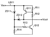
ここで、従来のヒステリシスを有する電源起動回路の構成を図5に示す。図5に示す従来のヒステリシスを有する電源起動回路は、ツェナーダイオードZD11及びZD12と、抵抗R11〜R14と、PNPトランジスタQ11と、NPNトランジスタQ12とを備えている。 Here, FIG. 5 shows a configuration of a power supply starting circuit having a conventional hysteresis. The conventional power supply startup circuit having hysteresis shown in FIG. 5 includes Zener diodes ZD11 and ZD12, resistors R11 to R14, a PNP transistor Q11, and an NPN transistor Q12.
入力電圧VINが供給されるラインLN11にツェナーダイオードZD11のカソードが接続され、ツェナーダイオードZD11のアノードが抵抗R14の一端に接続される。 The cathode of the Zener diode ZD11 is connected to the line LN11 to which the input voltage V IN is supplied, and the anode of the Zener diode ZD11 is connected to one end of the resistor R14.
また、NPNトランジスタQ12のベースが抵抗R13を介してツェナーダイオードZD11と抵抗R14との接続ノードに接続される。そして、ラインLN11に抵抗R11の一端が接続され、抵抗R11の他端が抵抗R12の一端に接続され、抵抗R12の他端がNPNトランジスタQ12のコレクタに接続され、NPNトランジスタQ12のエミッタと抵抗R14の他端とが共通接続される。 The base of the NPN transistor Q12 is connected to the connection node between the Zener diode ZD11 and the resistor R14 via the resistor R13. One end of the resistor R11 is connected to the line LN11, the other end of the resistor R11 is connected to one end of the resistor R12, the other end of the resistor R12 is connected to the collector of the NPN transistor Q12, the emitter of the NPN transistor Q12, and the resistor R14. Are connected in common with the other end.
また、PNPトランジスタQ11のベースが抵抗R11と抵抗R12との接続ノードに接続される。そして、ラインLN11にPNPトランジスタQ11のエミッタが接続され、PNPトランジスタQ11のコレクタがツェナーダイオードZD12のカソードに接続され、ツェナーダイオードZD12のアノードがツェナーダイオードZD11と抵抗R14との接続ノードに接続される。なお、ツェナーダイオードZD11のツェナー電圧が、オン状態であるときのPNPトランジスタQ11のコレクタ・エミッタ間電圧とツェナーダイオードZD12のツェナー電圧との合計値より大きくなるように、ツェナーダイオードZD11及びZD12をそれぞれ選定する。 The base of the PNP transistor Q11 is connected to a connection node between the resistor R11 and the resistor R12. The emitter of the PNP transistor Q11 is connected to the line LN11, the collector of the PNP transistor Q11 is connected to the cathode of the Zener diode ZD12, and the anode of the Zener diode ZD12 is connected to the connection node between the Zener diode ZD11 and the resistor R14. The Zener diodes ZD11 and ZD12 are selected so that the Zener voltage of the Zener diode ZD11 is larger than the sum of the collector-emitter voltage of the PNP transistor Q11 and the Zener voltage of the Zener diode ZD12 when the Zener diode ZD11 is in the ON state. To do.
上記のような構成の図5に示す従来のヒステリシスを有する電源起動回路は、以下のように動作する。 The conventional power supply starting circuit having hysteresis as shown in FIG. 5 operates as follows.
入力電圧VINがツェナーダイオードZD11のツェナー電圧未満である場合、ツェナーダイオードZD11、NPNトランジスタQ12、PNPトランジスタQ11、及びツェナーダイオードZD12がいずれもオフ状態となり、図5に示す従来のヒステリシスを有する電源起動回路は非動作状態である。 When the input voltage V IN is less than the Zener voltage of the Zener diode ZD11, the Zener diode ZD11, the NPN transistor Q12, the PNP transistor Q11, and the Zener diode ZD12 are all turned off, and the power supply having the conventional hysteresis shown in FIG. The circuit is inactive.
一方、入力電圧VINが立ち上がってツェナーダイオードZD11のツェナー電圧を越えると、ツェナーダイオードZD11がオン状態になり、ツェナーダイオードZD11及び抵抗R14の直列回路が、抵抗R13を介してNPNトランジスタQ12のベースにバイアス電圧を供給し、NPNトランジスタQ12をオン状態にする。そして、NPNトランジスタQ12がオン状態になると、抵抗R11、抵抗R12、及びNPNトランジスタQ12の直列回路が、PNPトランジスタQ11のベースにバイアス電圧を供給し、PNPトランジスタQ11をオン状態にする。 On the other hand, when the input voltage V IN rises and exceeds the Zener voltage of the Zener diode ZD11, the Zener diode ZD11 is turned on, and the series circuit of the Zener diode ZD11 and the resistor R14 is connected to the base of the NPN transistor Q12 via the resistor R13. A bias voltage is supplied to turn on the NPN transistor Q12. When the NPN transistor Q12 is turned on, a series circuit of the resistor R11, the resistor R12, and the NPN transistor Q12 supplies a bias voltage to the base of the PNP transistor Q11, and turns on the PNP transistor Q11.
PNPトランジスタQ11がオン状態になると、PNPトランジスタQ11のコレクタ・エミッタ間電圧とツェナーダイオードZD12のツェナー電圧との合計値がツェナーダイオードZD11のツェナー電圧より小さくなるので、ツェナーダイオードZD12がオン状態になり、ツェナーダイオードZD11がオフ状態になる。そして、PNPトランジスタQ11、ツェナーダイオードZD12及び抵抗R14の直列回路が、抵抗R13を介してNPNトランジスタQ12のベースにバイアス電圧を供給し、NPNトランジスタQ12のオン状態を維持する。NPNトランジスタQ12、PNPトランジスタQ11、ツェナーダイオードZD12のオン状態は、PNPトランジスタQ11のコレクタ・エミッタ間電圧とツェナーダイオードZD12のツェナー電圧との合計値を入力電圧VINが下回らない限り、維持される。 When the PNP transistor Q11 is turned on, the total value of the collector-emitter voltage of the PNP transistor Q11 and the Zener voltage of the Zener diode ZD12 is smaller than the Zener voltage of the Zener diode ZD11, so that the Zener diode ZD12 is turned on. Zener diode ZD11 is turned off. A series circuit of the PNP transistor Q11, the Zener diode ZD12, and the resistor R14 supplies a bias voltage to the base of the NPN transistor Q12 via the resistor R13, and maintains the ON state of the NPN transistor Q12. The ON state of the NPN transistor Q12, the PNP transistor Q11, and the Zener diode ZD12 is maintained as long as the input voltage VIN does not fall below the total value of the collector-emitter voltage of the PNP transistor Q11 and the Zener voltage of the Zener diode ZD12.
PNPトランジスタQ11がオン状態である場合、PNPトランジスタQ11とツェナーダイオードZD12との接続ノードの電圧である出力電圧VOUTがHighレベルとなり、図5に示す従来のヒステリシスを有する電源起動回路が動作状態となる。 When the PNP transistor Q11 is in the ON state, the output voltage V OUT which is the voltage at the connection node between the PNP transistor Q11 and the Zener diode ZD12 becomes High level, and the conventional power supply startup circuit having hysteresis shown in FIG. Become.
上記の通り、図5に示す従来のヒステリシスを有する電源起動回路は、オン状態であるときのPNPトランジスタQ11のコレクタ・エミッタ間電圧とツェナーダイオードZD12のツェナー電圧との合計値をツェナーダイオードZD11のツェナー電圧から差分して得られる電圧値によってヒステリシス量が決まる回路となっている。 As described above, the power supply starting circuit having the conventional hysteresis shown in FIG. 5 has the total value of the collector-emitter voltage of the PNP transistor Q11 and the Zener voltage of the Zener diode ZD12 in the on state. In this circuit, the amount of hysteresis is determined by the voltage value obtained by difference from the voltage.
従来のヒステリシスを有する電源起動回路は、2つのツェナーダイオードが並列接続されている構成しか提案されていなかった。 Only a configuration in which two Zener diodes are connected in parallel has been proposed as a conventional power supply starting circuit having hysteresis.
本発明は、上記の状況に鑑み、2つのツェナーダイオードが並列接続されている構成を採用せずにヒステリシスを持たすことができる電源起動回路及びスイッチング電源装置を提供して技術の豊富化を図ることを目的とする。 In view of the above situation, the present invention provides a power supply start circuit and a switching power supply device that can have hysteresis without adopting a configuration in which two Zener diodes are connected in parallel, and to enrich the technology. With the goal.
上記目的を達成するために本発明に係る電源起動回路は、第1の定電圧降下手段および第2の定電圧降下手段の直列回路と、入力電圧が所定値を超え、前記第1の定電圧降下手段及び前記第2の定電圧降下手段がオン状態になると、オン状態になる第1トランジスタと、前記第1トランジスタがオン状態になると、オン状態になる第2トランジスタを有し、前記第2トランジスタがオン状態になると、前記第2の定電圧降下手段をバイパスするバイパス回路とを備え、前記バイパス回路の電圧降下が前記第2の定電圧降下手段の電圧降下よりも小さい構成とする。 In order to achieve the above object, a power supply starting circuit according to the present invention includes a series circuit of first constant voltage drop means and second constant voltage drop means, an input voltage exceeding a predetermined value, and the first constant voltage drop means A first transistor that is turned on when the lowering means and the second constant voltage dropping means are turned on; a second transistor that is turned on when the first transistor is turned on; And a bypass circuit that bypasses the second constant voltage drop means when the transistor is turned on, the voltage drop of the bypass circuit is smaller than the voltage drop of the second constant voltage drop means.
このような構成によると、第1の定電圧降下手段と第2の定電圧降下手段との直列回路を備えるので、2つのツェナーダイオードが並列接続されている構成を採用せずにすむ。また、このような構成によると、前記トランジスタがオン状態になると、前記第2の定電圧降下手段をバイパスするバイパス回路とを備えるので、ヒステリシスを持たすことができる。 According to such a configuration, since the series circuit of the first constant voltage drop means and the second constant voltage drop means is provided, it is not necessary to employ a configuration in which two Zener diodes are connected in parallel. In addition, according to such a configuration, when the transistor is turned on, the bypass circuit that bypasses the second constant voltage drop means is provided, so that hysteresis can be provided.
また、前記第1の定電圧降下手段及び前記第2の定電圧降下手段をそれぞれツェナーダイオードとすることが好ましい。これにより、前記第1の定電圧降下手段及び前記第2の定電圧降下手段を少ない部品点数で実現することができる。 Preferably, the first constant voltage drop means and the second constant voltage drop means are respectively zener diodes. Thereby, the first constant voltage drop means and the second constant voltage drop means can be realized with a small number of parts.
また、前記トランジスタをPNPトランジスタ又はPチャネル電界効果トランジスタとしてもよい。これにより、電源起動回路の出力を反転させるためのトランジスタを別途設ける必要がなくなる。 The transistor may be a PNP transistor or a P-channel field effect transistor. This eliminates the need for a separate transistor for inverting the output of the power supply starting circuit.
また、上記目的を達成するために本発明に係るスイッチング電源装置は、上記いずれかの構成の電源起動回路を備える構成とする。 In order to achieve the above object, a switching power supply according to the present invention includes a power supply startup circuit having any one of the above configurations.
本発明によると、2つのツェナーダイオードが並列接続されている構成を採用せずにヒステリシスを持たすことができる電源起動回路及びスイッチング電源装置を実現することができ、技術の豊富化を図ることができる。 According to the present invention, it is possible to realize a power supply startup circuit and a switching power supply device that can have hysteresis without adopting a configuration in which two Zener diodes are connected in parallel, and the technology can be enriched. .
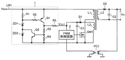
本発明の実施形態について図面を参照して以下に説明する。本発明に係るスイッチング電源装置の一構成例を図1に示す。図1に示す本発明に係るスイッチング電源装置は、本発明に係る電源起動回路1と、PWM制御回路2と、一次巻線L1、二次巻線L2、及び補助巻線L3を有するトランスと、スイッチング素子SW1と、整流ダイオードD1及びD2と、平滑コンデンサC1及びC2と、フォトカプラPC1とを備えている。
Embodiments of the present invention will be described below with reference to the drawings. An example of the configuration of the switching power supply according to the present invention is shown in FIG. The switching power supply device according to the present invention shown in FIG. 1 includes a power supply start circuit 1 according to the present invention, a
入力電圧VINが立ち上がって所定値を越えると、本発明に係る電源起動回路1が動作を開始して、PWM制御回路2に電力を供給し、PWM制御回路2を起動させる。起動後のPWM制御回路2は、フォトカプラPC1を介して送られてくる出力電圧VOの情報に応じてPWM(Pulse Width Modulation)信号を生成し、その生成したPWMをスイッチング素子SW1の制御端子に供給し、スイッチング素子SW1をオン/オフ制御する。
When the input voltage V IN rises and exceeds a predetermined value, the power supply start circuit 1 according to the present invention starts operating, supplies power to the
スイッチング素子SW1がオン状態のとき、入力電圧VINがトランスの一次巻線L1に供給され、トランスの一次巻線L1に励磁エネルギが蓄積される。一方、スイッチング素子SW1がオフ状態のとき、トランスの一次巻線L1に蓄積された励磁エネルギがトランスの二次巻線L2及び補助巻線L3から取り出される。したがって、トランスの二次巻線L2及び補助巻線L3から出力される電圧は矩形波状の交流電圧となる。 When the switching element SW1 is in the ON state, the input voltage V IN is supplied to the primary winding L1 of the transformer, and excitation energy is accumulated in the primary winding L1 of the transformer. On the other hand, when the switching element SW1 is in the off state, the excitation energy accumulated in the primary winding L1 of the transformer is taken out from the secondary winding L2 and the auxiliary winding L3 of the transformer. Accordingly, the voltage output from the secondary winding L2 and the auxiliary winding L3 of the transformer is a rectangular-wave AC voltage.
トランスの二次巻線L2から出力される矩形波状の交流電圧は整流ダイオードD2及び平滑コンデンサC2からなる整流平滑回路によって整流且つ平滑されて出力電圧VOとなる。そして、この出力電圧VOが負荷(不図示)に供給される。 The rectangular AC voltage output from the secondary winding L2 of the transformer is rectified and smoothed by the rectifying / smoothing circuit including the rectifying diode D2 and the smoothing capacitor C2, and becomes the output voltage V O. The output voltage V O is supplied to a load (not shown).
また、トランスの補助巻線L3から出力される矩形波状の交流電圧は整流ダイオードD1及び平滑コンデンサC1からなる整流平滑回路によって整流且つ平滑されてPWM制御回路2に供給される。したがって、平滑コンデンサC1の充電完了後は、整流ダイオードD1及び平滑コンデンサC1からなる整流平滑回路からPWM制御回路2の電源電圧をとることができる。
The rectangular wave AC voltage output from the auxiliary winding L3 of the transformer is rectified and smoothed by a rectifying / smoothing circuit including a rectifying diode D1 and a smoothing capacitor C1, and is supplied to the
次に、本発明に係る電源起動回路1について説明する。本発明に係る電源起動回路1は、ツェナーダイオードZD1及びZD2と、抵抗R1〜R5と、PNPトランジスタQ1と、NPNトランジスタQ2とを備えている。 Next, the power supply starting circuit 1 according to the present invention will be described. The power supply starting circuit 1 according to the present invention includes Zener diodes ZD1 and ZD2, resistors R1 to R5, a PNP transistor Q1, and an NPN transistor Q2.
入力電圧VINが供給されるラインLN1に抵抗R1の一端が接続され、抵抗R1の他端にツェナーダイオードZD1のカソードが接続され、ツェナーダイオードZD11のアノードがツェナーダイオードZD2のカソードに接続される。 One end of the resistor R1 is connected to the line LN1 to which the input voltage V IN is supplied, the cathode of the Zener diode ZD1 is connected to the other end of the resistor R1, and the anode of the Zener diode ZD11 is connected to the cathode of the Zener diode ZD2.
また、PNPトランジスタQ1のベースが抵抗R2を介して抵抗R1とツェナーダイオードZD1との接続ノードに接続される。そして、ラインLN1にPNPトランジスタQ1のエミッタが接続され、PNPトランジスタQ1のコレクタが抵抗R3の一端に接続され、抵抗R3の他端が抵抗R4の一端に接続される。 The base of the PNP transistor Q1 is connected to a connection node between the resistor R1 and the Zener diode ZD1 via the resistor R2. The emitter of the PNP transistor Q1 is connected to the line LN1, the collector of the PNP transistor Q1 is connected to one end of the resistor R3, and the other end of the resistor R3 is connected to one end of the resistor R4.
また、NPNトランジスタQ2のベースが抵抗R3と抵抗R4との接続ノードに接続される。そして、NPNトランジスタQ2のコレクタがツェナーダイオードZD1とツェナーダイオードZD2との接続ノードに接続され、NPNトランジスタQ2のエミッタとツェナーダイオードZD2のアノードと抵抗R4の他端とが共通接続される。なお、ツェナーダイオードZD2のツェナー電圧が、オン状態であるときのNPNトランジスタQ2のコレクタ・エミッタ間電圧より大きくなるように、ツェナーダイオードZD2を選定する。 The base of the NPN transistor Q2 is connected to a connection node between the resistor R3 and the resistor R4. The collector of the NPN transistor Q2 is connected to the connection node between the Zener diode ZD1 and the Zener diode ZD2, and the emitter of the NPN transistor Q2, the anode of the Zener diode ZD2, and the other end of the resistor R4 are connected in common. Note that the Zener diode ZD2 is selected so that the Zener voltage of the Zener diode ZD2 is larger than the collector-emitter voltage of the NPN transistor Q2 when it is in the on state.
上記のような構成の本発明に係る電源起動回路1は、以下のように動作する。 The power supply startup circuit 1 according to the present invention configured as described above operates as follows.
入力電圧VINが立ち上がりの初期の状態で、入力電圧VINがツェナーダイオードZD1のツェナー電圧(以下、第1ツェナー電圧という)とツェナーダイオードZD2のツェナー電圧(以下、第2ツェナー電圧という)との合計値未満である場合、抵抗R1の両端に電位差が生じないため、ツェナーダイオードZD1、ツェナーダイオードZD2、PNPトランジスタQ1、及びNPNトランジスタQ2がいずれもオフ状態となり、本発明に係る電源起動回路1は非動作状態である。 In the initial state of rising the input voltage V IN, the input voltage V IN is the Zener voltage of the Zener diode ZD1 (hereinafter referred to as the first zener voltage) zener voltage of the zener diode ZD2 (hereinafter, referred to as a second Zener voltage) of the If it is less than the total value, no potential difference is generated across the resistor R1, so that the Zener diode ZD1, Zener diode ZD2, PNP transistor Q1, and NPN transistor Q2 are all turned off. Non-operating state.
一方、入力電圧VINが立ち上がって、入力電圧VINが第1ツェナー電圧と第2ツェナー電圧との合計値を越えると、ツェナーダイオードZD1及びZD2がオン状態になり、抵抗R1の両端に電位差が生じる。それにより、抵抗R1並びにツェナーダイオードZD1及びZD2の直列回路が、抵抗R2を介してPNPトランジスタQ1のベースにバイアス電圧を供給し、PNPトランジスタQ1をオン状態にする。そして、PNPトランジスタQ1がオン状態になると、PNPトランジスタQ1、抵抗R3、及び抵抗R4の直列回路が、NPNトランジスタQ2のベースにバイアス電圧を供給し、NPNトランジスタQ2をオン状態にする。 On the other hand, when the input voltage V IN rises and the input voltage V IN exceeds the total value of the first Zener voltage and the second Zener voltage, the Zener diodes ZD1 and ZD2 are turned on, and there is a potential difference across the resistor R1. Arise. Thereby, the series circuit of the resistor R1 and the Zener diodes ZD1 and ZD2 supplies a bias voltage to the base of the PNP transistor Q1 via the resistor R2, thereby turning on the PNP transistor Q1. When the PNP transistor Q1 is turned on, the series circuit of the PNP transistor Q1, the resistor R3, and the resistor R4 supplies a bias voltage to the base of the NPN transistor Q2, and turns on the NPN transistor Q2.
NPNトランジスタQ2がオン状態になると、NPNトランジスタQ2のコレクタ・エミッタ間電圧が第2ツェナー電圧より小さくなるので、ツェナーダイオードZD2がオフ状態になる。そして、抵抗R1、ツェナーダイオードZD1、及びNPNトランジスタQ2の直列回路が、抵抗R2を介してPNPトランジスタQ1のベースにバイアス電圧を供給し、PNPトランジスタQ1のオン状態を維持する。NPNトランジスタQ2、PNPトランジスタQ1、ツェナーダイオードZD1のオン状態は、第1ツェナー電圧とNPNトランジスタQ2のコレクタ・エミッタ間電圧との合計値を入力電圧VINが下回らない限り、維持される。 When the NPN transistor Q2 is turned on, the collector-emitter voltage of the NPN transistor Q2 becomes smaller than the second Zener voltage, so that the Zener diode ZD2 is turned off. Then, the series circuit of the resistor R1, the Zener diode ZD1, and the NPN transistor Q2 supplies a bias voltage to the base of the PNP transistor Q1 through the resistor R2, and maintains the ON state of the PNP transistor Q1. The ON state of the NPN transistor Q2, the PNP transistor Q1, and the Zener diode ZD1 is maintained as long as the input voltage VIN does not fall below the total value of the first Zener voltage and the collector-emitter voltage of the NPN transistor Q2.
PNPトランジスタQ1がオン状態である場合、PNPトランジスタQ1と抵抗R3の接続ノードの電圧を抵抗R5によって降圧した電圧VOUTがHighレベルとなり、本発明に係る電源起動回路1が動作状態となる。 When the PNP transistor Q1 is in the ON state, the voltage V OUT obtained by stepping down the voltage at the connection node between the PNP transistor Q1 and the resistor R3 by the resistor R5 becomes the High level, and the power supply starting circuit 1 according to the present invention is in the operating state.
上記の通り、本発明に係る電源起動回路1は、第2ツェナー電圧からオン状態であるときのNPNトランジスタQ2のコレクタ・エミッタ間電圧を差分して得られる電圧値によってヒステリシス量が決まるヒステリシスを有する電源起動回路となっている。 As described above, the power supply starting circuit 1 according to the present invention has a hysteresis whose hysteresis amount is determined by a voltage value obtained by subtracting the collector-emitter voltage of the NPN transistor Q2 when the second Zener voltage is in the on state. It is a power start circuit.
ツェナーダイオードZD1を正の温度特性を有するツェナーダイオード(ツェナー電圧が5.6Vより大きいツェナーダイオード)とし、ツェナーダイオードZD2を負の温度特性を有するツェナーダイオード(ツェナー電圧が5.6Vより小さいツェナーダイオード)とすることが望ましい。本発明に係る電源起動回路は、2つのツェナーダイオードが直列接続されている構成であるので、ツェナーダイオードZD1の正の温度特性とツェナーダイオードZD2の負の温度特性とが互いに低減し合うように作用し、電源起動回路が動作を開始する入力電圧VINの値の温度によるばらつきが小さくなり、電源起動回路が動作を開始する入力電圧VINの値が安定する。 The Zener diode ZD1 is a Zener diode having a positive temperature characteristic (a Zener diode having a Zener voltage larger than 5.6V), and the Zener diode ZD2 is a Zener diode having a negative temperature characteristic (Zener diode having a Zener voltage smaller than 5.6V). Is desirable. Since the power start circuit according to the present invention has a configuration in which two Zener diodes are connected in series, the positive temperature characteristic of the Zener diode ZD1 and the negative temperature characteristic of the Zener diode ZD2 act so as to reduce each other. and, the variation becomes small power start circuit according to the temperature values of the input voltage V iN to start the operation, the power supply starting circuit is the value of the input voltage V iN to start the operation is stabilized.
なお、本発明は上述した実施形態に限らず、発明の主旨を逸脱しない範囲で種々の変更を加えて実行することができる。 The present invention is not limited to the above-described embodiment, and can be executed with various modifications without departing from the spirit of the invention.
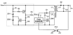
例えば、上述した実施形態では、本発明に係る電源起動回路で用いるトランジスタをバイポーラトランジスタとしていたが、バイポーラトランジスタの代わりに電界効果トランジスタを用いても構わない。すなわち、本発明に係る電源起動回路1において、PNPトランジスタQ1をPチャネル電界効果トランジスタに置換し、NPNトランジスタQ2をNチャネル電界効果トランジスタに置換して、図2に示すような構成にしてもよい。 For example, in the above-described embodiment, the transistor used in the power supply activation circuit according to the present invention is a bipolar transistor. However, a field effect transistor may be used instead of the bipolar transistor. That is, in the power supply startup circuit 1 according to the present invention, the PNP transistor Q1 may be replaced with a P-channel field effect transistor, and the NPN transistor Q2 may be replaced with an N-channel field effect transistor, so that the configuration shown in FIG. .
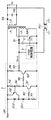
また、本発明に係る電源起動回路1では、抵抗R1並びにツェナーダイオードZD1及びZD2の直列回路において、ツェナーダイオードZD1及びZD2が抵抗R1よりも低電位側に配置され、抵抗R1並びにツェナーダイオードZD1及びZD2の直列回路から供給されるバイアス電圧を制御端子に入力するトランジスタをPNPトランジスタQ1としていたが、抵抗及び2つのツェナーダイオードの直列回路において、2つのツェナーダイオードが抵抗よりも高電位側に配置され、抵抗及び2つのツェナーダイオードの直列回路から供給されるバイアス電圧を制御端子に入力するトランジスタをNPNトランジスタ又はNチャネル電界トランジスタとしても構わない。かかる構成の一例を図3に示す。 Further, in the power supply starting circuit 1 according to the present invention, in the series circuit of the resistor R1 and the Zener diodes ZD1 and ZD2, the Zener diodes ZD1 and ZD2 are arranged on the lower potential side than the resistor R1, and the resistor R1 and the Zener diodes ZD1 and ZD2 The transistor that inputs the bias voltage supplied from the series circuit to the control terminal is the PNP transistor Q1, but in the series circuit of the resistor and the two Zener diodes, the two Zener diodes are arranged on the higher potential side than the resistor, A transistor that inputs a bias voltage supplied from a series circuit of a resistor and two Zener diodes to the control terminal may be an NPN transistor or an N-channel field transistor. An example of such a configuration is shown in FIG.
図3に示す本発明に係る電源起動回路1’は、ツェナーダイオードZD1’及びZD2’と、抵抗R1’〜R5’と、抵抗R6及びR7と、NPNトランジスタQ1’と、PNPトランジスタQ2’と、NPNトランジスタQ3と、抵抗R6及びR7とを備えている。なお、NPNトランジスタQ1’及びQ3はそれぞれNチャネル電界トランジスタとの置き換えが可能であり、PNPトランジスタQ2’はPチャネル電界トランジスタとの置き換えが可能である。 3 includes a Zener diode ZD1 ′ and ZD2 ′, resistors R1 ′ to R5 ′, resistors R6 and R7, an NPN transistor Q1 ′, and a PNP transistor Q2 ′. An NPN transistor Q3 and resistors R6 and R7 are provided. NPN transistors Q1 'and Q3 can each be replaced with an N-channel field transistor, and PNP transistor Q2' can be replaced with a P-channel field transistor.
入力電圧VINが供給されるラインLN1にツェナーダイオードZD2’のカソードが接続され、ツェナーダイオードZD2’のアノードがツェナーダイオードZD1’のカソードに接続され、ツェナーダイオードZD1’のアノードが抵抗R1’の一端に接続される。 The cathode of the Zener diode ZD2 ′ is connected to the line LN1 to which the input voltage V IN is supplied, the anode of the Zener diode ZD2 ′ is connected to the cathode of the Zener diode ZD1 ′, and the anode of the Zener diode ZD1 ′ is one end of the resistor R1 ′. Connected to.
また、NPNトランジスタQ1’のベースが抵抗R2’を介してツェナーダイオードZD1’と抵抗R1’との接続ノードに接続される。そして、ラインLN1に抵抗R3’の一端が接続され、抵抗R3’の他端に抵抗R4’の一端が接続され、抵抗R4’の他端がNPNトランジスタQ1’のコレクタに接続される。 The base of the NPN transistor Q1 'is connected to a connection node between the Zener diode ZD1' and the resistor R1 'via the resistor R2'. One end of the resistor R3 'is connected to the line LN1, the other end of the resistor R4' is connected to the other end of the resistor R3 ', and the other end of the resistor R4' is connected to the collector of the NPN transistor Q1 '.
また、ラインLN1にPNPトランジスタQ2’のエミッタが接続され、PNPトランジスタQ2’のコレクタがツェナーダイオードZD2’とツェナーダイオードZD1’との接続ノードに接続され、PNPトランジスタQ2’のベースが抵抗R3’と抵抗R4’との接続ノードに接続される。 Further, the emitter of the PNP transistor Q2 ′ is connected to the line LN1, the collector of the PNP transistor Q2 ′ is connected to the connection node between the Zener diode ZD2 ′ and the Zener diode ZD1 ′, and the base of the PNP transistor Q2 ′ is connected to the resistor R3 ′. It is connected to a connection node with the resistor R4 ′.
さらに、ラインLN1に抵抗R6の一端が接続され、抵抗R6の他端がNPNトランジスタQ3のコレクタに接続され、NPNトランジスタQ3のベースが抵抗R5’を介して抵抗R4’とNPNトランジスタQ1’との接続ノードに接続され、抵抗R1’の他端とNPNトランジスタQ1’のエミッタとNPNトランジスタQ3のエミッタとが共通接続される。なお、ツェナーダイオードZD2’のツェナー電圧(以下、第2’ツェナー電圧という)が、オン状態であるときのPNPトランジスタQ2’のコレクタ・エミッタ間電圧より大きくなるように、ツェナーダイオードZD2’を選定する。 Furthermore, one end of the resistor R6 is connected to the line LN1, the other end of the resistor R6 is connected to the collector of the NPN transistor Q3, and the base of the NPN transistor Q3 is connected between the resistor R4 ′ and the NPN transistor Q1 ′ via the resistor R5 ′. The other end of the resistor R1 ′, the emitter of the NPN transistor Q1 ′, and the emitter of the NPN transistor Q3 are connected in common to the connection node. Note that the Zener diode ZD2 ′ is selected so that the Zener voltage of the Zener diode ZD2 ′ (hereinafter referred to as the second “Zener voltage”) is larger than the collector-emitter voltage of the PNP transistor Q2 ′ when the Zener diode ZD2 ′ is in the ON state. .
上記のような構成の本発明に係る電源起動回路1’は、以下のように動作する。 The power supply startup circuit 1 'according to the present invention having the above-described configuration operates as follows.
入力電圧VINが立ち上がりの初期の状態で、入力電圧VINがツェナーダイオードZD1’のツェナー電圧(以下、第1’ツェナー電圧という)と第2’ツェナー電圧との合計値未満である場合、ツェナーダイオードZD1’、ツェナーダイオードZD2’、NPNトランジスタQ1’、及びPNPトランジスタQ2’がいずれもオフ状態となり、NPNトランジスタQ3のみがオン状態となり、本発明に係る電源起動回路1は非動作状態である。 When the input voltage V IN is in the initial state of rising, and the input voltage V IN is less than the total value of the zener voltage of the zener diode ZD1 ′ (hereinafter referred to as the first ′ zener voltage) and the second ′ zener voltage, The diode ZD1 ′, the Zener diode ZD2 ′, the NPN transistor Q1 ′, and the PNP transistor Q2 ′ are all turned off, and only the NPN transistor Q3 is turned on, and the power supply startup circuit 1 according to the present invention is in a non-operating state.
一方、入力電圧VINが立ち上がって、入力電圧VINが第1’ツェナー電圧と第2’ツェナー電圧との合計値を越えると、ツェナーダイオードZD1’及びZD2’がオン状態になり、抵抗R1’並びにツェナーダイオードZD1’及びZD2’の直列回路が、抵抗R2’を介してNPNトランジスタQ1’のベースにバイアス電圧を供給し、NPNトランジスタQ1’をオン状態にする。そして、NPNトランジスタQ1’がオン状態になると、NPNトランジスタQ1’、抵抗R3’、及び抵抗R4’の直列回路が、PNPトランジスタQ2’のベースにバイアス電圧を供給し、PNPトランジスタQ2’をオン状態にする。 On the other hand, when the input voltage V IN rises and the input voltage V IN exceeds the total value of the first ′ Zener voltage and the second ′ Zener voltage, the Zener diodes ZD1 ′ and ZD2 ′ are turned on and the resistor R1 ′ In addition, the series circuit of the Zener diodes ZD1 ′ and ZD2 ′ supplies a bias voltage to the base of the NPN transistor Q1 ′ via the resistor R2 ′, and turns on the NPN transistor Q1 ′. When the NPN transistor Q1 ′ is turned on, the series circuit of the NPN transistor Q1 ′, the resistor R3 ′, and the resistor R4 ′ supplies a bias voltage to the base of the PNP transistor Q2 ′, and the PNP transistor Q2 ′ is turned on. To.
PNPトランジスタQ2’がオン状態になると、PNPトランジスタQ2’のコレクタ・エミッタ間電圧が第2’ツェナー電圧より小さくなるので、ツェナーダイオードZD2’がオフ状態になる。そして、抵抗R1’、ツェナーダイオードZD1’、及びPNPトランジスタQ2’の直列回路が、抵抗R2’を介してNPNトランジスタQ1’のベースにバイアス電圧を供給し、NPNトランジスタQ1’のオン状態を維持する。PNPトランジスタQ2’、NPNトランジスタQ1’、ツェナーダイオードZD1’のオン状態は、第1’ツェナー電圧とPNPトランジスタQ2’のコレクタ・エミッタ間電圧との合計値を入力電圧VINが下回らない限り、維持される。 When the PNP transistor Q2 'is turned on, the collector-emitter voltage of the PNP transistor Q2' becomes smaller than the second 'zener voltage, so that the Zener diode ZD2' is turned off. The series circuit of the resistor R1 ′, the Zener diode ZD1 ′, and the PNP transistor Q2 ′ supplies a bias voltage to the base of the NPN transistor Q1 ′ via the resistor R2 ′, and maintains the ON state of the NPN transistor Q1 ′. . The ON state of the PNP transistor Q2 ′, the NPN transistor Q1 ′, and the Zener diode ZD1 ′ is maintained as long as the input voltage V IN is not lower than the total value of the first ′ Zener voltage and the collector-emitter voltage of the PNP transistor Q2 ′. Is done.
NPNトランジスタQ1’がオン状態である場合、NPNトランジスタQ1’と抵抗R3’の接続ノードの電圧を抵抗R5’によって降圧した電圧VOUTがLowレベルとなり、NPNトランジスタQ3がオフ状態になる。これにより、本発明に係る電源起動回路1’の出力電圧VOUTがHighレベルになり、本発明に係る電源起動回路1’が動作状態となる。 'When it is turned on, NPN transistors Q1' NPN transistor Q1 voltage V OUT obtained by stepping down 'the voltage at the connection node of the resistors R5' and the resistor R3 by becomes Low level, NPN transistor Q3 is turned off. As a result, the output voltage V OUT of the power supply startup circuit 1 ′ according to the present invention becomes a high level, and the power supply startup circuit 1 ′ according to the present invention enters an operating state.
上記の通り、本発明に係る電源起動回路1’は、第2’ツェナー電圧からオン状態であるときのPNPトランジスタQ2’のコレクタ・エミッタ間電圧を差分して得られる電圧値によってヒステリシス量が決まるヒステリシスを有する電源起動回路となっている。 As described above, in the power supply starting circuit 1 'according to the present invention, the amount of hysteresis is determined by the voltage value obtained by subtracting the collector-emitter voltage of the PNP transistor Q2' when the second 'Zener voltage is on. This is a power supply starting circuit having hysteresis.
ツェナーダイオードZD1’を正の温度特性を有するツェナーダイオード(ツェナー電圧が5.6Vより大きいツェナーダイオード)とし、ツェナーダイオードZD2’を負の温度特性を有するツェナーダイオード(ツェナー電圧が5.6Vより小さいツェナーダイオード)とすることが望ましい。本発明に係る電源起動回路は、2つのツェナーダイオードが直列接続されている構成であるので、ツェナーダイオードZD1’の正の温度特性とツェナーダイオードZD2’の負の温度特性とが互いに低減し合うように作用し、電源起動回路が動作を開始する入力電圧VINの値の温度によるばらつきが小さくなり、電源起動回路が動作を開始する入力電圧VINの値が安定する。 The Zener diode ZD1 ′ is a Zener diode having a positive temperature characteristic (a Zener diode having a Zener voltage larger than 5.6V), and the Zener diode ZD2 ′ is a Zener diode having a negative temperature characteristic (a Zener voltage having a Zener voltage smaller than 5.6V). It is desirable to use a diode. Since the power supply starting circuit according to the present invention has a configuration in which two Zener diodes are connected in series, the positive temperature characteristic of the Zener diode ZD1 ′ and the negative temperature characteristic of the Zener diode ZD2 ′ are mutually reduced. act on, the variation decreases the power start circuit according to the temperature values of the input voltage V iN to start the operation, the power supply starting circuit is the value of the input voltage V iN to start the operation is stabilized.
また、上述した実施形態では、定電圧降下手段としてツェナーダイオードを用いたが、ツェナーダイオードの代わりに、他の定電圧降下手段を用いても構わない。例えば、定電圧の精度はさほど高くないが、ダイオードを縦続接続したものを定電圧降下手段として用いてもよい。図5に示す従来のヒステリシスを有する電源起動回路では、ツェナーダイオードZD11及びZD12のツェナー電圧がいずれも大きいため、ツェナーダイオードZD11の代わりにダイオードを縦続接続したものに用いる場合も、ツェナーダイオードZD12の代わりにダイオードを縦続接続したものに用いる場合も縦続数を多くする必要がある。これに対して、本発明に係る電源起動回路では、ヒステリシス量に依存するが、通常ツェナーダイオードZD2のツェナー電圧は2V程度に設定するので、ツェナーダイオードZD2の代わりにダイオードを縦続接続したものに用いる場合は、縦続数を3個程度に抑えることができる。 In the above-described embodiment, the Zener diode is used as the constant voltage drop means. However, other constant voltage drop means may be used instead of the Zener diode. For example, the accuracy of the constant voltage is not so high, but a diode connected in cascade may be used as the constant voltage drop means. In the power supply startup circuit having the conventional hysteresis shown in FIG. 5, the zener voltages of the zener diodes ZD11 and ZD12 are both large. Therefore, when the zener diode ZD11 is used instead of the zener diode ZD11, Even when the diodes are connected in cascade, it is necessary to increase the number of cascades. On the other hand, in the power supply starting circuit according to the present invention, although depending on the amount of hysteresis, the Zener voltage of the Zener diode ZD2 is normally set to about 2V, so that the Zener diode ZD2 is used for a cascade connection of diodes. In this case, the cascade number can be reduced to about 3.
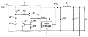
また、上述した実施形態では、トランスを有するスイッチング電源装置を例示したが、本発明に係るスイッチング電源装置はトランスを有するスイッチング電源装置に限定されることはなく、いわゆるトランスレス型スイッチング電源装置であっても構わない。つまり、本発明はスイッチング電源装置全般に適用することができる。 In the above-described embodiment, the switching power supply device having the transformer has been exemplified. However, the switching power supply device according to the present invention is not limited to the switching power supply device having the transformer, and is a so-called transformerless switching power supply device. It doesn't matter. That is, the present invention can be applied to switching power supply devices in general.
ここで、本発明に係るトランスレス型スイッチング電源装置の一構成例を図4に示す。なお、図4において図1と同一の部分には同一の符号を付し、詳細な説明を省略する。 Here, FIG. 4 shows a configuration example of the transformerless switching power supply device according to the present invention. 4 that are the same as those in FIG. 1 are denoted by the same reference numerals, and detailed description thereof is omitted.
入力電圧VINが立ち上がって所定値を越えると、本発明に係る電源起動回路1が動作を開始して、PWM制御回路3に電力を供給し、PWM制御回路3を起動させる。起動後のPWM制御回路3は、送られてくる出力電圧VOの情報に応じてPWM信号を生成し、その生成したPWMをスイッチング素子SW2の制御端子に供給し、スイッチング素子SW2をオン/オフ制御する。 When the input voltage V IN rises and exceeds a predetermined value, the power supply start circuit 1 according to the present invention starts operation, supplies power to the PWM control circuit 3, and starts the PWM control circuit 3. After startup, the PWM control circuit 3 generates a PWM signal according to the information of the output voltage V O sent thereto, supplies the generated PWM to the control terminal of the switching element SW2, and turns on / off the switching element SW2. Control.
スイッチング素子SW2がオン状態のときには、ラインLN1からスイッチング素子SW2を介してコイルL4に電流が流れる。これにより、コイルL4にエネルギが蓄えられ、かつ負荷(不図示)にエネルギが供給される。一方、スイッチング素子SW2がオフ状態のときには、コイルL4に蓄えられたエネルギがダイオードD3を通じて負荷(不図示)に供給される。 When the switching element SW2 is on, a current flows from the line LN1 to the coil L4 via the switching element SW2. Thereby, energy is stored in the coil L4, and energy is supplied to a load (not shown). On the other hand, when the switching element SW2 is in the off state, the energy stored in the coil L4 is supplied to a load (not shown) through the diode D3.
1、1’ 本発明に係る電源起動回路
2、3 PWM制御回路2
C1、C2 平滑コンデンサ
C3 コンデンサ
D1、D2 整流ダイオード
D3 ダイオード
L1 トランスの一次巻線
L2 トランスの二次巻線
L3 トランスの補助巻線L3
L4 コイル
LN1 入力電圧が供給されるライン
PC1 フォトカプラ
Q1、Q2’ PNPトランジスタ
Q2、Q1’、Q3 NPNトランジスタ
R1〜R5、R1’〜R5’、R6、R7 抵抗
SW1、SW2 スイッチング素子
ZD1、ZD2、ZD1’、ZD2’ ツェナーダイオード
1, 1 'power
C1, C2 Smoothing capacitor C3 Capacitor D1, D2 Rectifier diode D3 Diode L1 Primary winding of transformer L2 Secondary winding of transformer L3 Auxiliary winding L3 of transformer
L4 Coil LN1 Line to which input voltage is supplied PC1 Photocoupler Q1, Q2 'PNP transistors Q2, Q1', Q3 NPN transistors R1-R5, R1'-R5 ', R6, R7 Resistors SW1, SW2 Switching elements ZD1, ZD2, ZD1 ', ZD2' Zener diode
Claims (4)
入力電圧が所定値を超え、前記第1の定電圧降下手段及び前記第2の定電圧降下手段がオン状態になると、オン状態になる第1トランジスタと、
前記第1トランジスタがオン状態になると、オン状態になる第2トランジスタを有し、前記第2トランジスタがオン状態になると、前記第2の定電圧降下手段をバイパスするバイパス回路とを備え、
前記バイパス回路の電圧降下が前記第2の定電圧降下手段の電圧降下よりも小さいことを特徴とする電源起動回路。 A series circuit of first constant voltage drop means and second constant voltage drop means;
A first transistor that is turned on when an input voltage exceeds a predetermined value and the first constant voltage drop means and the second constant voltage drop means are turned on;
A second circuit that includes a second transistor that is turned on when the first transistor is turned on, and that bypasses the second constant voltage drop unit when the second transistor is turned on;
A power supply starting circuit, wherein a voltage drop of the bypass circuit is smaller than a voltage drop of the second constant voltage drop means.
Priority Applications (1)
| Application Number | Priority Date | Filing Date | Title |
|---|---|---|---|
| JP2008314868A JP2010142002A (en) | 2008-12-10 | 2008-12-10 | Power supply start-up circuit and switching power supply device |
Applications Claiming Priority (1)
| Application Number | Priority Date | Filing Date | Title |
|---|---|---|---|
| JP2008314868A JP2010142002A (en) | 2008-12-10 | 2008-12-10 | Power supply start-up circuit and switching power supply device |
Publications (1)
| Publication Number | Publication Date |
|---|---|
| JP2010142002A true JP2010142002A (en) | 2010-06-24 |
Family
ID=42351618
Family Applications (1)
| Application Number | Title | Priority Date | Filing Date |
|---|---|---|---|
| JP2008314868A Pending JP2010142002A (en) | 2008-12-10 | 2008-12-10 | Power supply start-up circuit and switching power supply device |
Country Status (1)
| Country | Link |
|---|---|
| JP (1) | JP2010142002A (en) |
Cited By (4)
| Publication number | Priority date | Publication date | Assignee | Title |
|---|---|---|---|---|
| CN104065257A (en) * | 2014-06-25 | 2014-09-24 | 深圳市汇川技术股份有限公司 | A Hysteretic Startup Circuit for Power Supply Control Chip |
| JP2016010222A (en) * | 2014-06-24 | 2016-01-18 | 三菱電機株式会社 | Power start circuit |
| CN110171370A (en) * | 2018-02-20 | 2019-08-27 | 三菱电机株式会社 | Starting circuit |
| JP2019208258A (en) * | 2019-07-24 | 2019-12-05 | 三菱電機株式会社 | Starting circuit |
Citations (4)
| Publication number | Priority date | Publication date | Assignee | Title |
|---|---|---|---|---|
| JPS61109458A (en) * | 1984-10-30 | 1986-05-27 | Hitachi Metals Ltd | Switching power source |
| JPH11187644A (en) * | 1997-12-18 | 1999-07-09 | Ishikawajima Harima Heavy Ind Co Ltd | Power activation control circuit |
| JP2000197356A (en) * | 1998-12-25 | 2000-07-14 | Fuji Electric Co Ltd | Power control circuit |
| JP2004222472A (en) * | 2003-01-17 | 2004-08-05 | Fuji Electric Device Technology Co Ltd | Switching power supply control circuit |
-
2008
- 2008-12-10 JP JP2008314868A patent/JP2010142002A/en active Pending
Patent Citations (4)
| Publication number | Priority date | Publication date | Assignee | Title |
|---|---|---|---|---|
| JPS61109458A (en) * | 1984-10-30 | 1986-05-27 | Hitachi Metals Ltd | Switching power source |
| JPH11187644A (en) * | 1997-12-18 | 1999-07-09 | Ishikawajima Harima Heavy Ind Co Ltd | Power activation control circuit |
| JP2000197356A (en) * | 1998-12-25 | 2000-07-14 | Fuji Electric Co Ltd | Power control circuit |
| JP2004222472A (en) * | 2003-01-17 | 2004-08-05 | Fuji Electric Device Technology Co Ltd | Switching power supply control circuit |
Cited By (6)
| Publication number | Priority date | Publication date | Assignee | Title |
|---|---|---|---|---|
| JP2016010222A (en) * | 2014-06-24 | 2016-01-18 | 三菱電機株式会社 | Power start circuit |
| CN104065257A (en) * | 2014-06-25 | 2014-09-24 | 深圳市汇川技术股份有限公司 | A Hysteretic Startup Circuit for Power Supply Control Chip |
| CN110171370A (en) * | 2018-02-20 | 2019-08-27 | 三菱电机株式会社 | Starting circuit |
| CN110171370B (en) * | 2018-02-20 | 2022-07-26 | 三菱电机株式会社 | Starting circuit |
| JP2019208258A (en) * | 2019-07-24 | 2019-12-05 | 三菱電機株式会社 | Starting circuit |
| JP7042775B2 (en) | 2019-07-24 | 2022-03-28 | 三菱電機株式会社 | Startup circuit |
Similar Documents
| Publication | Publication Date | Title |
|---|---|---|
| KR100630855B1 (en) | Circuit and method for controlling dc-dc converter | |
| CN1996732B (en) | Switch power device and semiconductor device using same | |
| JP3450929B2 (en) | Switching power supply | |
| JP6424644B2 (en) | Semiconductor device for power control | |
| JP2004062331A (en) | DC power supply | |
| JP5293016B2 (en) | DC-DC converter | |
| JP2005300376A (en) | Voltage detection circuit, power supply device and semiconductor device | |
| JP2010051053A (en) | Control circuit for boost dc-dc converters and boost dc-dc converter | |
| CN101164220A (en) | Power source control method and structure thereof | |
| CN110401347B (en) | DC power supply unit | |
| US6538492B2 (en) | Power supply, electronic device using the same, and output | |
| JP2015041571A (en) | LED power supply device and LED lighting device | |
| JP2008048515A (en) | Switching power supply | |
| JP2016144310A (en) | Switching power supply | |
| JP2010142002A (en) | Power supply start-up circuit and switching power supply device | |
| JP2015216763A (en) | Switching power supply circuit | |
| JP3757260B2 (en) | Synchronous rectification type DC-DC converter | |
| CN114144966A (en) | Converter with holding circuit and surge control circuit | |
| JP2003339157A (en) | Self-excited switching power supply | |
| JP6455180B2 (en) | Power supply control semiconductor device | |
| JP2009095182A (en) | Switching power-supply device | |
| JP3544370B2 (en) | Switching power supply | |
| JP7575260B2 (en) | Switching Power Supply Unit | |
| JP2004320858A (en) | Switching power supply | |
| JP6774359B2 (en) | Switching power supply |
Legal Events
| Date | Code | Title | Description |
|---|---|---|---|
| A621 | Written request for application examination |
Free format text: JAPANESE INTERMEDIATE CODE: A621 Effective date: 20100903 |
|
| A977 | Report on retrieval |
Free format text: JAPANESE INTERMEDIATE CODE: A971007 Effective date: 20120509 |
|
| A131 | Notification of reasons for refusal |
Free format text: JAPANESE INTERMEDIATE CODE: A131 Effective date: 20120515 |
|
| A02 | Decision of refusal |
Free format text: JAPANESE INTERMEDIATE CODE: A02 Effective date: 20120918 |