JP2010141784A - Display device, organic electroluminescence display panel, and correction value processing method - Google Patents
Display device, organic electroluminescence display panel, and correction value processing method Download PDFInfo
- Publication number
- JP2010141784A JP2010141784A JP2008318218A JP2008318218A JP2010141784A JP 2010141784 A JP2010141784 A JP 2010141784A JP 2008318218 A JP2008318218 A JP 2008318218A JP 2008318218 A JP2008318218 A JP 2008318218A JP 2010141784 A JP2010141784 A JP 2010141784A
- Authority
- JP
- Japan
- Prior art keywords
- pixel
- value
- correction
- correction value
- pixels
- Prior art date
- Legal status (The legal status is an assumption and is not a legal conclusion. Google has not performed a legal analysis and makes no representation as to the accuracy of the status listed.)
- Granted
Links
Images


Landscapes
- Devices For Indicating Variable Information By Combining Individual Elements (AREA)
- Transforming Electric Information Into Light Information (AREA)
Abstract
【課題】各画素の発光輝度を光センサで測定して各画素が所要の輝度で発光するように各画素に与える表示データ信号を補正する。この場合に、各光センサの検出ばらつきの影響を受けないで補正値を得ることができるようにし、さらに表示実行中も補正値を修正する。
【解決手段】少なくとも2以上の画素に対して、各画素から等距離の位置に光センサを設ける。そして一方の画素の発光輝度と他方の画素の発光輝度を、等距離に配置された1つの光センサで検出することで、光センサの検出ばらつきの影響の無い補正値を算出する。さらに他の画素に対しても、既に補正値を更新した画素を一部に用いながら順次連鎖的に補正値を求めていくことで、表示画面を構成する全画素について、光センサの検出ばらつきの影響を排除した補正値を得る。表示実行中はダミー画素を用いて画素劣化を判定し、劣化状況に応じて補正値を修正する。
【選択図】図15A display data signal applied to each pixel is corrected so that each pixel emits light with a required luminance by measuring the light emission luminance of each pixel with an optical sensor. In this case, the correction value can be obtained without being affected by the detection variation of each optical sensor, and the correction value is corrected even during display execution.
An optical sensor is provided at a position equidistant from each pixel for at least two or more pixels. Then, the light emission luminance of one pixel and the light emission luminance of the other pixel are detected by one photosensor arranged at the same distance, thereby calculating a correction value that is not affected by the detection variation of the photosensor. Furthermore, for other pixels, the correction values are sequentially calculated while using some of the pixels whose correction values have already been updated. A correction value that eliminates the influence is obtained. During display execution, pixel deterioration is determined using dummy pixels, and the correction value is corrected according to the deterioration state.
[Selection] Figure 15
Description
本発明は表示装置と、表示装置における補正値処理方法に関する。また有機エレクトロルミネッセンス表示パネルに関する。 The present invention relates to a display device and a correction value processing method in the display device. The present invention also relates to an organic electroluminescence display panel.
例えば有機エレクトロルミネッセンス(EL:Electroluminescence)発光素子を用いた表示装置など、自発光素子を用いた表示装置では、画素間の発光輝度のばらつきを無くして画面上に生じるムラを無くすことが重要である。
画素の発光輝度のばらつきは、パネル製造時の初期状態でも生じるが、経時変化によっても生じる。
For example, in a display device using a self-luminous element such as a display device using an organic electroluminescence (EL) light emitting element, it is important to eliminate unevenness in light emission luminance between pixels and eliminate unevenness on the screen. .
The variation in the light emission luminance of the pixel occurs even in the initial state when the panel is manufactured, but also due to a change with time.
上記特許文献1,2では、各画素回路内に光センサを配置して、光センサの検出値をパネル内でフィードバックして発光輝度を補正する方式や、光センサからシステムにフィードバックして補正する方式が開示されている。
In
各画素の発光輝度を光センサで測定して、発光輝度が所要の輝度となるように画素に与える信号値を補正することで、画素間の輝度ばらつきを解消できる。
しかしながら、上記特許文献1,2のように、1つの画素について、その画素回路内に1つのセンサを設けて輝度検出を行う方式の場合、光センサ同士の検出ばらつきが生じてしまう。光センサ自体も初期状態或いは経時劣化により検出特性の変動があるため、各光センサ同士での検出ばらつきは排除できない。
すると光センサ同士のばらつきの影響が補正に表れ、適切に画素の発光輝度のばらつきを解消することができないこととなる。
By measuring the light emission luminance of each pixel with an optical sensor and correcting the signal value given to the pixel so that the light emission luminance becomes the required luminance, the luminance variation between the pixels can be eliminated.
However, in the case of the method of performing luminance detection by providing one sensor in the pixel circuit for one pixel as in
Then, the influence of the variation between the optical sensors appears in the correction, and the variation in the light emission luminance of the pixels cannot be appropriately eliminated.
本発明では、各画素の発光輝度を光センサで測定して、各画素が所要の輝度で発光するように各画素に与える表示データ信号を補正する方式を採る。この場合に、各光センサの検出ばらつきの影響を受けないようにし、画面上のむらが適切に解消されるような精度の高い補正が実行できるようにする。さらにその上で、通常の表示動作実行中も補正値が適切に更新されるようにすることを目的とする。 In the present invention, a method is employed in which the light emission luminance of each pixel is measured by an optical sensor, and the display data signal applied to each pixel is corrected so that each pixel emits light at a required luminance. In this case, it is possible to perform correction with high accuracy so as not to be affected by detection variation of each optical sensor and to appropriately eliminate unevenness on the screen. Furthermore, an object of the present invention is to appropriately update the correction value even during execution of a normal display operation.
本発明の表示装置は、画面有効領域を形成する画素と画面有効領域外のダミー画素とを含む複数の発光画素を有し、またそれぞれが少なくとも2以上の発光画素から等距離の位置となるように配置された複数の光センサを有する表示パネル部と、上記表示パネル部の各画素を、入力された表示データ信号に基づいて発光駆動する表示駆動部と、上記各発光画素のそれぞれについての補正値を記憶する補正値格納部と、信号処理部とを備える。上記信号処理部は、通常表示動作を行わない際に、2以上の発光画素について基準表示データ信号値でのそれぞれの発光輝度を、当該2以上の発光画素から等距離に配置された光センサの検出値として取り込み、取り込んだ各検出値に基づいて、当該2以上の発光画素のうちの一の発光画素に対する他の発光画素の補正値を算出して当該他の発光画素についての補正値として上記補正値格納部に格納させる補正値設定処理を、各光センサに対応する2以上の発光画素について順次行うことで、補正値設定対象とした全発光画素の補正値を設定するとともに、通常表示動作時には、上記補正値格納部に格納された補正値を用いて各発光画素の発光輝度補正が行われるようにし、また所定タイミングで補正値更新処理として、上記ダミー画素の発光輝度の変化値を検出し、検出した発光輝度の変化値に基づいて、上記補正値格納部に格納された各発光画素の補正値を修正して更新する。 The display device of the present invention has a plurality of light emitting pixels including a pixel forming a screen effective area and a dummy pixel outside the screen effective area, and each is located at an equidistance from at least two or more light emitting pixels. A display panel unit having a plurality of photosensors arranged on the display panel, a display driving unit that drives each pixel of the display panel unit to emit light based on an input display data signal, and correction for each of the light emitting pixels A correction value storage unit for storing values and a signal processing unit are provided. When the signal processing unit does not perform the normal display operation, the light emission luminance at the reference display data signal value for two or more light-emitting pixels is set at an equal distance from the two or more light-emitting pixels. Based on each detected value captured as a detection value, a correction value of another light emitting pixel for one light emitting pixel of the two or more light emitting pixels is calculated, and the correction value for the other light emitting pixel is calculated as the correction value for the other light emitting pixel. A correction value setting process to be stored in the correction value storage unit is sequentially performed for two or more light emitting pixels corresponding to each light sensor, thereby setting correction values for all light emitting pixels that are correction value setting targets and performing a normal display operation. Sometimes, the emission luminance correction of each light emitting pixel is performed using the correction value stored in the correction value storage unit, and the dummy pixel generation is performed as a correction value update process at a predetermined timing. Detecting a change in value of the luminance based on the change value of the detected emission brightness, and updates to correct the correction value of each light emitting pixels which are stored in the correction value storing unit.
また、画面有効領域を形成する各発光画素に与える表示データ信号値の積算値をそれぞれ格納する積算値格納部をさらに備え、上記信号処理部は、画面有効領域を形成する各発光画素に与える表示データ信号値をそれぞれ積算して上記積算値格納部に記憶させていくとともに、上記補正値更新処理の際には、上記ダミー画素の発光輝度の変化値と、画面有効領域の各発光画素について上記積算値格納部に記憶された積算値とに基づいて補正値の修正値を求め、該修正値を用いて上記補正値格納部に格納された各発光画素の補正値を修正して更新する。
また、上記信号処理部は、上記通常表示動作時において上記補正値更新処理を行わない期間には、上記ダミー画素についても、上記補正値格納部に格納された補正値を用いて補正した表示データ信号を与えて発光させるようにする。
また、ダミー画素の発光輝度の測定値を格納するダミー測定値格納部をさらに備え、上記信号処理部は、上記補正値更新処理の際に、上記ダミー画素の発光輝度を検出し、検出した発光輝度を、上記ダミー測定値格納部に記憶された前回の補正値更新処理の際に測定した発光輝度と比較して発光輝度の変化値を求めるととともに、上記ダミー測定値格納部の測定値を今回の測定値に更新する処理を行う。
Further, the image processing apparatus further includes an integrated value storage unit that stores an integrated value of display data signal values to be given to each light emitting pixel forming the screen effective area, and the signal processing unit has a display to be given to each light emitting pixel forming the screen effective area. Each of the data signal values is integrated and stored in the integrated value storage unit, and at the time of the correction value update processing, the change value of the light emission luminance of the dummy pixel and the light emission pixel of the screen effective area are described above. A correction value of the correction value is obtained based on the integrated value stored in the integrated value storage unit, and the correction value of each light emitting pixel stored in the correction value storage unit is corrected and updated using the correction value.
Further, the signal processing unit corrects the display data corrected by using the correction value stored in the correction value storage unit for the dummy pixels during the period when the correction value update processing is not performed during the normal display operation. Give a signal to emit light.
In addition, a dummy measurement value storage unit that stores a measurement value of the emission luminance of the dummy pixel is further provided, and the signal processing unit detects the emission luminance of the dummy pixel during the correction value update process, and detects the detected light emission. The luminance is compared with the emission luminance measured during the previous correction value update process stored in the dummy measurement value storage unit to obtain a change value of the emission luminance, and the measurement value of the dummy measurement value storage unit is obtained. Update the current measurement value.
また上記信号処理部は、上記通常表示動作時において上記補正値更新処理を行わない期間には、複数の上記ダミー画素のそれぞれについて、それぞれ所定の基準表示データ信号値を与えて発光させるようにし、上記補正値更新処理の際には、それぞれの上記ダミー画素の発光輝度の変化値を、上記積算値格納部に記憶された積算値を用いて画面有効領域の各発光画素に対応させ、各発光画素について対応する変化値を用いて補正値の修正値を求め、該修正値を用いて上記補正値格納部に格納された各発光画素の補正値を修正して更新する。
また上記発光画素は、有機エレクトロルミネッセンス発光素子を用いた画素である。
In addition, the signal processing unit emits light by giving a predetermined reference display data signal value to each of the plurality of dummy pixels during a period when the correction value update processing is not performed during the normal display operation. At the time of the correction value update process, the change value of the emission luminance of each dummy pixel is made to correspond to each light emission pixel in the screen effective region using the integrated value stored in the integrated value storage unit, and each light emission The correction value of the correction value is obtained using the corresponding change value for the pixel, and the correction value of each light emitting pixel stored in the correction value storage unit is corrected and updated using the correction value.
The light emitting pixel is a pixel using an organic electroluminescence light emitting element.
本発明の有機エレクトロルミネッセンス表示パネルは、画面有効領域を形成する画素と画面有効領域外のダミー画素とを含む複数の発光画素を有し、またそれぞれが少なくとも2以上の発光画素から等距離の位置となるように配置された複数の光センサを有する。 The organic electroluminescence display panel of the present invention has a plurality of light emitting pixels including pixels that form a screen effective region and dummy pixels outside the screen effective region, and each is located at an equidistant position from at least two or more light emitting pixels. A plurality of photosensors arranged to be
本発明の補正値処理方法は、画面有効領域を形成する画素と画面有効領域外のダミー画素とを含む複数の発光画素を有し、またそれぞれが少なくとも2以上の発光画素から等距離の位置となるように配置された複数の光センサを有する表示パネル部と、上記表示パネル部の各画素を、入力された表示データ信号に基づいて発光駆動する表示駆動部と、上記各発光画素のそれぞれについての補正値を記憶する補正値格納部と、通常表示動作時には、上記補正値格納部に格納された補正値を用いて各画素の発光輝度補正が行われるようにする信号処理部とを備えた表示装置の補正値処理方法である。そして、通常表示動作を行わない際に、2以上の発光画素について基準表示データ信号値でのそれぞれの発光輝度を、当該2以上の発光画素から等距離に配置された光センサで検出し、当該2以上の発光画素についての各検出値に基づいて、当該2以上の発光画素のうちの一の発光画素に対する他の発光画素の補正値を算出し、算出された補正値を、当該他の発光画素についての補正値として上記補正値格納部に格納させる補正値設定処理を、各光センサに対応する2以上の発光画素について順次行うことで、補正値設定対象とした全発光画素の補正値を設定する。また通常表示動作時には、所定タイミングで、上記ダミー画素の発光輝度の変化値を検出し、検出した発光輝度の変化値に基づいて、上記補正値格納部に格納された各発光画素の補正値を修正して更新する補正値更新処理を行う。 The correction value processing method of the present invention has a plurality of light emitting pixels including a pixel that forms a screen effective area and a dummy pixel outside the screen effective area, and each is located at a position equidistant from at least two or more light emitting pixels. A display panel unit having a plurality of photosensors arranged in such a manner, a display driving unit that drives each pixel of the display panel unit to emit light based on an input display data signal, and each of the light emitting pixels A correction value storage unit that stores the correction value of the pixel, and a signal processing unit that performs light emission luminance correction of each pixel using the correction value stored in the correction value storage unit during the normal display operation. It is a correction value processing method of a display device. Then, when the normal display operation is not performed, the respective light emission luminances at the reference display data signal value for two or more light emitting pixels are detected by an optical sensor arranged at an equal distance from the two or more light emitting pixels, Based on each detection value for two or more light-emitting pixels, a correction value of another light-emitting pixel for one light-emitting pixel of the two or more light-emitting pixels is calculated, and the calculated correction value is used as the other light emission. The correction value setting process to be stored in the correction value storage unit as the correction value for the pixel is sequentially performed for two or more light-emitting pixels corresponding to each photosensor, so that the correction values of all the light-emitting pixels targeted for correction value setting are obtained. Set. In the normal display operation, the change value of the light emission luminance of the dummy pixel is detected at a predetermined timing, and the correction value of each light emission pixel stored in the correction value storage unit is determined based on the detected change value of the light emission luminance. A correction value update process for correcting and updating is performed.
これらの本発明では、少なくとも2以上の画素に対して、各画素から等距離の位置に光センサを設ける。そして、一方の画素の発光輝度と、他方の画素の発光輝度を、当該等距離に配置された1つの光センサで検出する。すると、共通の光センサで各画素の輝度検出値が得られるため、光センサの検出ばらつきの影響の無い補正値を算出できる。つまり1つの光センサから等距離の2以上の画素において、それらが基準表示データ信号値に対して同輝度の発光が行われるように補正値を得ることができる。
これを、さらに他の画素に対しても、既に補正値を更新した画素を一部に用いながら順次連鎖的に実行していけば、補正対象とする全画素について、光センサの検出ばらつきの影響を排除した補正値を得ることができる。
このような補正値設定処理は、例えばパワーオン時/パワーオフ時など、通常の表示動作を行わない期間に行うことになる。
一方、通常の表示動作実行中には、ダミー画素を用いて劣化の進行具合を検出し、それに基づいて有効画素(画面有効領域を形成する発光画素)の劣化を予測して、補正値を修正していく。
機器の用い方によっては、通常表示動作が長時間にわたることもある。例えば常時表示を実行している表示装置の場合、上記のパワーオン時等の補正値の設定の機会がなかなか訪れないという事態が生ずる。また通常の表示動作実行中は、有効画素は表示データ信号に基づく発光動作中であるので、有効画素に補正値設定のための基準表示データ信号値を与えることもできない。ところが長時間の表示継続により、画素の劣化が生じ、発光輝度が変化していく。このような場合、補正値が適正な値ではなくなってしまう場合がある。
そこで、通常の表示動作実行中は、ダミー画素を用いて劣化進行具合を判定し、それに基づいて有効画素の劣化を予測し、補正値を修正していく。
このようにすることで、長時間、補正値設定処理ができなくても、適宜、補正値修正更新が行われ、適切な補正値が保持された状態とすることができる。
In the present invention, a photosensor is provided at a position equidistant from each pixel for at least two or more pixels. Then, the light emission luminance of one pixel and the light emission luminance of the other pixel are detected by one photosensor arranged at the same distance. Then, since the luminance detection value of each pixel is obtained by the common optical sensor, it is possible to calculate a correction value that is not affected by the detection variation of the optical sensor. That is, a correction value can be obtained in two or more pixels equidistant from one photosensor so that they emit light having the same luminance with respect to the reference display data signal value.
If this is performed sequentially for other pixels, using some of the pixels for which correction values have already been updated in a sequential manner, the influence of detection variations of the photosensors will be applied to all pixels to be corrected. It is possible to obtain a correction value that eliminates the above.
Such correction value setting processing is performed during a period in which a normal display operation is not performed, for example, at power-on / power-off.
On the other hand, during normal display operation, the progress of deterioration is detected using dummy pixels, and the correction value is corrected by predicting the deterioration of the effective pixels (light-emitting pixels that form the screen effective area) based on the detection. I will do it.
Depending on how the device is used, the normal display operation may take a long time. For example, in the case of a display device that is always performing display, there is a situation in which the opportunity for setting the correction value at the time of the power-on described above does not come easily. In addition, during the normal display operation, the effective pixel is in the light emission operation based on the display data signal, and therefore it is not possible to give a reference display data signal value for setting a correction value to the effective pixel. However, when the display is continued for a long time, the pixel is deteriorated and the light emission luminance is changed. In such a case, the correction value may not be an appropriate value.
Therefore, during normal display operation, the progress of deterioration is determined using dummy pixels, the deterioration of effective pixels is predicted based on this, and the correction value is corrected.
In this way, even if correction value setting processing cannot be performed for a long time, correction value correction / update is performed as appropriate, and an appropriate correction value can be held.
本発明によれば、画面を構成する各発光画素について、光センサの経時劣化等による検出ばらつきの影響を排除した補正値を求めることができ、各画素の発光ばらつきを補正できる。従って、表示画面上に表れる輝度ムラを適切に解消できる。
さらに通常の表示動作実行中にも、逐次補正値を修正する補正値更新処理が行われる。このため、長時間、パワーオン時等の補正値設定処理ができなくても、補正値が修正されることになり、各画素の劣化の進行等による画面上の輝度ムラ等の発生を抑えることができる。これらのことから、高品質な表示画像を得ることができる。
According to the present invention, for each light emitting pixel constituting the screen, a correction value that eliminates the influence of detection variation due to deterioration with time of the optical sensor or the like can be obtained, and the light emission variation of each pixel can be corrected. Therefore, luminance unevenness appearing on the display screen can be appropriately eliminated.
Furthermore, correction value update processing for correcting correction values is performed even during normal display operation execution. For this reason, even if correction value setting processing cannot be performed for a long time, such as when the power is turned on, the correction value is corrected, and the occurrence of uneven brightness on the screen due to the progress of deterioration of each pixel is suppressed. Can do. From these things, a high-quality display image can be obtained.
以下、本発明の実施の形態としての有機EL表示装置を説明していく。説明は次の順序で行う。
[1.有機EL表示装置の構成]
[2.パワーオン/オフ時の補正係数設定処理]
[3.補正係数設定処理例]
[4.通常の表示動作実行中の処理]
[5.第1の補正係数更新処理例]
[6.第2の補正係数更新処理例]
[7.変形例]
Hereinafter, an organic EL display device as an embodiment of the present invention will be described. The description will be given in the following order.
[1. Configuration of organic EL display device]
[2. Correction coefficient setting process at power on / off]
[3. Correction coefficient setting processing example]
[4. Processing during normal display operation]
[5. First correction coefficient update processing example]
[6. Second correction coefficient update processing example]
[7. Modified example]
[1.有機EL表示装置の構成]
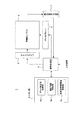
図1に実施の形態の表示装置1の要部の構成を示す。
本例の表示装置1は、有機EL素子を発光素子として用いるディスプレイパネルとして有機ELパネル5を有する。有機ELパネル5は、ゲートドライバ3及びデータドライバ4によって表示駆動される。
[1. Configuration of organic EL display device]
FIG. 1 shows a configuration of a main part of the
The
そして有機ELパネル5に対して供給する表示データ信号について処理を行う部位として、信号処理部2が設けられる。信号処理部2は、入力信号として表示データ信号が入力されると、その入力信号に対して例えば信号値補正などの所要の処理を行い、処理後の表示データ信号をデータドライバ4に出力する。また垂直同期信号、水平同期信号をゲートドライバ3及びデータドライバ4に供給する。
And the signal processing part 2 is provided as a site | part which processes about the display data signal supplied with respect to the
メモリ部6は、信号処理部2が補正処理に用いる各種情報を記憶する。例えば不揮発性メモリ等で構成される。
メモリ部6においては、記憶領域として、ダミー測定値格納部6a、補正係数格納部6b、画素信号積算値格納部6cが設けられる。
ダミー測定値格納部6aは、有機ELパネル5に形成されている後述するダミー画素についての発光輝度の測定値を格納する。
補正係数格納部6は、有機ELパネル5における各画素に対応した補正値として補正係数を格納する。この補正係数は、画素間の輝度ばらつきを解消するために設定された補正係数である。
画素信号積算値格納部6cは、各画素に与える表示データ信号値の積算値を格納する。各画素毎に例えば毎フレーム、又は所定間隔毎に、信号処理部2が表示データ信号値を積算していく。これは、或る期間において各画素に与える表示データ信号値の平均値を求めるための情報となり、また、その平均値は各画素毎に発光輝度の劣化の進行具合を予測させる情報とされる。
The
In the
The dummy measurement
The correction
The pixel signal integrated
通常の表示動作時には、信号処理部2は、補正係数格納部6bに格納された補正係数を用いて各画素の発光輝度補正が行われるようにする。例えば信号処理部2は、各画素に与える表示データ信号の信号値を、補正係数格納部6bに記憶された補正係数によって補正した上で、データドライバ4に出力する。表示データ信号値の補正処理としては、例えば、或る画素に対する表示データ信号値(発光輝度としての階調値)について、その画素に対して設定されている補正係数を乗算する処理などを行う。
なお、補正係数格納部6bに格納する補正値は乗算係数に限られず、例えば表示データ信号値に対して加減算を行う補正値などでもよい。
或いは補正係数格納部6bに格納する補正値は、表示データ信号の階調値自体を補正するものではなく、例えばデータドライバ4、ゲートドライバ3によって制御される画素回路の発光時間の制御値などであってもよい。その場合、信号処理部2は、補正値に基づいた発光期間制御信号をゲートドライバ3、データドライバ4に与えればよい。
いずれにしても補正係数格納部6bに格納する補正値は、各画素毎に発光輝度を調整するための値であればよい。
During a normal display operation, the signal processing unit 2 performs light emission luminance correction of each pixel using the correction coefficient stored in the correction
The correction value stored in the correction
Alternatively, the correction value stored in the correction
In any case, the correction value stored in the correction
信号処理部2が例えば表示データ信号に補正係数を乗算して補正を行ってデータドライバ4に出力することで、画素間の発光輝度ばらつきが解消され、表示画面上で輝度ムラが生じないようにされる。
仮に全画素を同一の表示データ信号値(階調値)で発光させると、本来は画面上では輝度ムラは生じないはずであるが、実際には各画素の経時劣化の進行具合等により、各画素には発光輝度ムラが生じる。
そのような各画素間の輝度ばらつきを解消する補正係数が設定され、補正係数格納部6に記憶されていれば、信号処理部2がその補正係数を用いて表示データ信号値の補正を行うことで、画面上の輝度ムラが解消されることになる。
For example, the signal processing unit 2 multiplies the display data signal by a correction coefficient to perform correction, and outputs the corrected data to the data driver 4, so that variations in emission luminance between pixels are eliminated and luminance unevenness does not occur on the display screen. Is done.
If all the pixels emit light with the same display data signal value (gradation value), luminance unevenness should not occur on the screen. The pixel has uneven luminance.
If a correction coefficient that eliminates such luminance variation between pixels is set and stored in the correction
検出信号生成部7は、後述するように有機ELパネル5に多数配置されている光センサで得られる検出値を信号処理部2に供給する。例えば各光センサの検出値をデジタルデータとして信号処理部2に供給する。
信号処理部2は、後述するように、有機ELパネル5内に多数配置されている光センサの検出値を用いて補正係数格納部6に記憶されている補正係数の設定を行う。例えばパワーオンの際などに補正係数設定処理を行う。その際、信号処理部2は検出信号生成部7から、所定の光センサの検出値を取り込むことになる。
また信号処理部2は、逐次所定時点(例えば一定時間毎など)に、補正係数を修正する補正係数更新処理を行う。この場合も、信号処理部2は検出信号生成部7から、所定の光センサ(ダミー画素に対する光センサ)の検出値を取り込むことになる。
As will be described later, the detection signal generation unit 7 supplies the signal processing unit 2 with detection values obtained by a large number of optical sensors arranged on the
As will be described later, the signal processing unit 2 sets correction coefficients stored in the correction
In addition, the signal processing unit 2 performs correction coefficient update processing for correcting the correction coefficient sequentially at predetermined time points (for example, at regular intervals). Also in this case, the signal processing unit 2 takes in a detection value of a predetermined photosensor (a photosensor for the dummy pixel) from the detection signal generation unit 7.
図2、図3を参照して有機ELパネル5、及び有機ELパネル5の駆動を行うゲートドライバ3、データドライバ4について述べる。
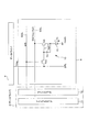
図2に有機ELパネル5、ゲートドライバ3、データドライバ4の構成の一例を示す。有機ELパネル5は、有機EL素子を発光素子とし、アクティブマトリクス方式で発光駆動を行う画素回路10を含むものである。
The
FIG. 2 shows an example of the configuration of the
図2に示すように、有機ELディスプレイパネルモジュール3は、画素回路10が列方向と行方向にマトリクス状に配列された画素アレイとして構成される。なお、画素回路10には「R」「G」「B」を付しているが、これはR(赤)、G(緑)、B(青)の各色の発光画素であることを示している。
As shown in FIG. 2, the organic EL
そして各画素回路10を駆動するため、データドライバ4と、ゲートドライバ3が設けられる。ゲートドライバ3はドライブスキャナ11とライトスキャナ12を備える。
またデータドライバ4により選択され、表示データ信号の信号値(階調値)に応じた電圧を画素回路10に供給する信号線DTL1、DTL2・・・が、画素アレイ上で列方向に配されている。信号線DTL1、DTL2・・・は、画素アレイにおいてマトリクス配置された画素回路10の列数分だけ配される。
A data driver 4 and a
Also, signal lines DTL1, DTL2,..., Which are selected by the data driver 4 and supply a voltage corresponding to the signal value (gradation value) of the display data signal to the
また画素アレイ上に、行方向に書込制御線WSL1,WSL2・・・、電源制御線DSL1,DSL2・・・が配されている。これらの書込制御線WSL及び電源制御線DSLは、それぞれ、画素アレイにおいてマトリクス配置された画素回路10の行数分だけ配される。
書込制御線WSL(WSL1,WSL2・・・)はライトスキャナ12により駆動される。ライトスキャナ12は、設定された所定のタイミングで、行状に配設された各書込制御線WSL1,WSL2・・・に順次、走査パルスWS(WS1,WS2・・・)を供給して、画素回路10を行単位で線順次走査する。
電源制御線DSL(DSL1,DSL2・・・)はドライブスキャナ11により駆動される。ドライブスキャナ11は、ライトスキャナ12による線順次走査に合わせて、行状に配設された各電源制御線DSL1,DSL2・・・に駆動電位(Vcc)、初期電位(Vini)の2値に切り替わる電源電圧としての電源パルスDS(DS1,DS2・・・)を供給する。
データドライバ4は、ライトスキャナ12による線順次走査に合わせて、列方向に配された信号線DTL1、DTL2・・・に対して、画素回路10に対する入力信号としての信号電位(Vsig)と基準電位(Vofs)を供給する。
On the pixel array, write control lines WSL1, WSL2,... And power supply control lines DSL1, DSL2,. These write control lines WSL and power supply control lines DSL are arranged by the number of rows of the
Write control lines WSL (WSL1, WSL2,...) Are driven by the
The power supply control lines DSL (DSL1, DSL2,...) Are driven by the
The data driver 4 applies a signal potential (Vsig) as an input signal to the
図3に画素回路10の構成例を示している。この画素回路10が、図2の構成における画素回路10のようにマトリクス配置される。なお、図3では簡略化のため、信号線DTLと書込制御線WSL及び電源制御線DSLが交差する部分に配される1つの画素回路10のみを示している。
FIG. 3 shows a configuration example of the
この画素回路10は、発光素子である有機EL素子15と、1個の保持容量Csと、サンプリングトランジスタTrS、駆動トランジスタTrDとしての2個の薄膜トランジスタ(TFT)とで構成されている。サンプリングトランジスタTrS、駆動トランジスタTrDはnチャネルTFTとされている。
The
保持容量Csは、一方の端子が駆動トランジスタTrDのソースに接続され、他方の端子が同じく駆動トランジスタTrDのゲートに接続されている。
画素回路10の発光素子は例えばダイオード構造の有機EL素子15とされ、アノードとカソードを備えている。有機EL素子15のアノードは駆動トランジスタTrDのソースsに接続され、カソードは所定の接地配線(カソード電位Vcath)に接続されている。
サンプリングトランジスタTrSは、そのドレインとソースの一端が信号線DTLに接続され、他端が駆動トランジスタTrDのゲートに接続される。またサンプリングトランジスタTrSのゲートは書込制御線WSLに接続されている。
駆動トランジスタTrDのドレインは電源制御線DSLに接続されている。
The holding capacitor Cs has one terminal connected to the source of the drive transistor TrD and the other terminal connected to the gate of the drive transistor TrD.
The light emitting element of the
The sampling transistor TrS has one end of its drain and source connected to the signal line DTL, and the other end connected to the gate of the driving transistor TrD. The gate of the sampling transistor TrS is connected to the write control line WSL.
The drain of the drive transistor TrD is connected to the power control line DSL.
有機EL素子15の発光駆動は、基本的には次のようになる。
信号線DTLに信号電位Vsigが印加されたタイミングで、サンプリングトランジスタTrSが書込制御線WSLによってライトスキャナ12から与えられる走査パルスWSによって導通される。これにより信号線DTLからの入力信号Vsigが保持容量Csに書き込まれる。駆動トランジスタTrDは、ドライブスキャナ11によって駆動電位Vccが与えられている電源制御線DSLからの電流供給により、保持容量Csに保持された信号電位に応じた電流IELを有機EL素子15に流し、有機EL素子15を発光させる。
The light emission driving of the
At the timing when the signal potential Vsig is applied to the signal line DTL, the sampling transistor TrS is turned on by the scanning pulse WS supplied from the
つまり、各フレーム期間において、画素信号値(階調値)が保持容量Csに書き込まれる動作が行われるが、これにより、階調値によって駆動トランジスタTrDのゲート−ソース間電圧Vgsが決まる。駆動トランジスタTrDは飽和領域で動作することで有機EL素子15に対して定電流源として機能し、ゲート−ソース間電圧Vgsに応じた電流IELを有機EL素子15に流す。これによって有機EL素子15では、階調値に応じた輝度の発光が行われる。
That is, in each frame period, the pixel signal value (gradation value) is written into the storage capacitor Cs. With this, the gate-source voltage Vgs of the drive transistor TrD is determined by the gradation value. The drive transistor TrD functions as a constant current source for the
各画素回路10に与えられる信号電位Vsigは、その画素に対する表示データ信号値に応じた電圧である。上述のように信号処理部2は、補正係数格納部6bに記憶された各画素回路10についての補正係数を用いて、各画素に対する表示データ信号値を補正してデータドライバ4に供給する。
このため、各画素回路10毎に、入力信号電位Vsigに対する発光輝度のばらつきがあったとしても、入力信号電位Vsig自体が補正されていることにより、各画素回路10においては、それぞれ求められる本来の輝度の発光が行われる。これによって画面表示上での輝度ムラが解消されることになる。
The signal potential Vsig applied to each
For this reason, even if there is a variation in light emission luminance with respect to the input signal potential Vsig for each
[2.パワーオン/オフ時の補正係数設定処理]
ところで、そのように表示データ信号の信号値補正によって画面上での輝度ムラを解消させるためには、補正係数が適切に設定されていることが前提となる。
特に各画素回路10毎の発光輝度のばらつき具合は、経時劣化によっても変化するため、補正係数格納部6bに記憶された補正係数も、適宜更新されていかなければ、常に輝度ムラのない高品質な画面表示を行うことができない。
[2. Correction coefficient setting process at power on / off]
By the way, in order to eliminate luminance unevenness on the screen by correcting the signal value of the display data signal in this way, it is assumed that the correction coefficient is set appropriately.
In particular, the degree of variation in light emission luminance for each
本実施の形態の表示装置1では、例えばパワーオンにより起動される際、又はパワーオフで終了処理を行う際の一方又は両方で、補正係数の設定処理を行い、補正係数格納部6bに記憶されている補正係数を、その時点で適切な値に設定する。
In the
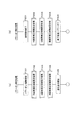
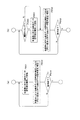
図4(a)(b)にパワーオン時の処理及びパワーオフ時の処理を示している。
ユーザの操作、もしくはシステム接続された機器からの指令、或いは表示装置1内部のタイマー機能などにより、図1には示していない表示装置1の制御部が、パワーオン要求の発生を認識すると、図4(a)の処理が行われる。
即ち図示しない制御部は、ステップF101として、電源回路から各部への電源供給を開始させると共に、所要の起動処理を行う。また制御部は、信号処理部2に補正係数設定処理を指示する。
FIGS. 4A and 4B show processing at power-on and processing at power-off.
When the control unit of the display device 1 (not shown in FIG. 1) recognizes the occurrence of a power-on request by a user operation, a command from a device connected to the system, or a timer function in the
That is, a control unit (not shown) starts power supply from the power supply circuit to each unit and performs a required activation process as step F101. The control unit also instructs the signal processing unit 2 to perform correction coefficient setting processing.
信号処理部2はステップF102として、有機ELパネル5におけるR画素についての補正係数設定処理を行う。
この補正係数設定処理は、例えば少なくとも有効画像領域における全R画素を補正値設定処理の対象として行い、当該全R画素についての補正係数格納部6bに格納される補正係数の設定を行う処理である。
またステップF103でG画素についての補正係数設定処理を行う。
この補正係数設定処理は、例えば少なくとも有効画像領域における全G画素を補正値設定処理の対象として行い、当該全G画素についての補正係数格納部6bに格納される補正係数の設定を行う処理である。
さらにステップF104としてB画素についての補正係数設定処理を行う。
この補正係数設定処理は、例えば少なくとも有効画像領域における全B画素を補正値設定処理の対象として行い、当該全B画素についての補正係数格納部6bに格納される補正係数の設定を行う処理である。
これらの補正係数設定処理により、補正係数格納部6bに格納されている、各画素回路10毎の補正係数がその時点で適切な値に設定されたことになる。具体的な補正係数設定処理例については後述する。
In step F102, the signal processing unit 2 performs a correction coefficient setting process for the R pixel in the
This correction coefficient setting process is a process for performing, for example, at least all R pixels in the effective image region as targets for the correction value setting process and setting correction coefficients stored in the correction
In step F103, correction coefficient setting processing for the G pixel is performed.
This correction coefficient setting process is a process for performing, for example, at least all G pixels in the effective image area as targets for the correction value setting process, and setting correction coefficients stored in the correction
In step F104, correction coefficient setting processing for the B pixel is performed.
This correction coefficient setting process is a process for performing, for example, at least all B pixels in the effective image area as targets for the correction value setting process and setting correction coefficients stored in the correction
By these correction coefficient setting processes, the correction coefficient for each
これらの補正係数設定処理が終了したら、ステップF105で通常表示を開始する。即ち信号処理部2は、入力される表示データ信号の信号値について、それぞれ画素単位で補正係数を補正係数格納部6bから読み出し、信号値を補正してデータドライバ4に供給する動作を開始する。
これによって通常の表示状態においては、最新の補正係数によって補正された表示データ信号に基づき、輝度ムラのない表示動作が行われる。
When these correction coefficient setting processes are completed, normal display is started in step F105. That is, the signal processing unit 2 starts the operation of reading the correction coefficient from the correction
As a result, in a normal display state, a display operation without luminance unevenness is performed based on the display data signal corrected by the latest correction coefficient.
このようなパワーオン時(起動時)ではなく、或いはパワーオン時に加えて、パワーオフ時に補正係数の設定処理を行っても良い。
例えば制御部は、ユーザ操作、タイマー機能、システム接続機器からの指示等として、表示装置1の電源オフの要求が発生した場合に、図4(b)の処理を行う。
まずステップF201で、信号処理部2に対して通常の表示動作を終了させる指示を行う。また制御部は、信号処理部2に補正係数設定処理を指示する。
信号処理部2はステップF202として、有機ELパネル5におけるR画素についての補正係数設定処理を行う。またステップF203でG画素についての補正係数設定処理を行い、さらにステップF204としてB画素についての補正係数設定処理を行う。
これらの補正係数設定処理により、補正係数格納部6bに格納されている各画素回路10毎の補正係数がその時点で適切な値に設定される。
その後制御部はステップF205で、所要の終了処理を行い、また電源回路に各部への電源供給を停止させる指示を行って電源オフ状態とする。
The correction coefficient setting process may be performed at power-off in addition to power-on (start-up) or power-on.
For example, the control unit performs the process of FIG. 4B when a power-off request for the
First, in step F201, the signal processing unit 2 is instructed to end a normal display operation. The control unit also instructs the signal processing unit 2 to perform correction coefficient setting processing.
In step F202, the signal processing unit 2 performs a correction coefficient setting process for the R pixel in the
By these correction coefficient setting processes, the correction coefficient for each
Thereafter, in step F205, the control unit performs a necessary end process, and instructs the power supply circuit to stop power supply to each unit to turn off the power.
以上の図4(a)又は図4(b)のいずれかの処理が少なくとも行われることで、補正係数格納部6に記憶された補正係数は、適宜更新設定されることになり、通常表示動作時には各画素の経時劣化にも対応した発光輝度補正が実現される。
The correction coefficient stored in the correction
[3.補正係数設定処理例]
以下、具体的な補正係数設定処理例について説明していく。なお、図4(a)(b)では、R、G、Bの各画素群について順次補正係数設定処理を行うとしたが、補正係数設定処理自体は同様であるため、以下ではR画素群に対する補正係数設定処理についてのみ述べる。即ち図4(a)のステップF102又は図4(b)のステップF202の処理である。ステップF103,F104、又はステップF203,F204の処理は、対象とする画素群及び使用する光センサが異なるのみで、以下説明する補正係数設定処理が同様に行われると理解すればよい。
[3. Correction coefficient setting processing example]
Hereinafter, a specific example of the correction coefficient setting process will be described. 4A and 4B, the correction coefficient setting process is sequentially performed for each of the R, G, and B pixel groups. However, since the correction coefficient setting process itself is the same, hereinafter, the correction coefficient setting process is performed for the R pixel group. Only the correction coefficient setting process will be described. That is, it is the process of step F102 in FIG. 4A or step F202 in FIG. It should be understood that the processing of steps F103 and F104 or steps F203 and F204 is the same as the correction coefficient setting processing described below, except that the target pixel group and the photosensor used are different.
補正係数設定処理を図5〜図7により説明する。
まず図5、図6で画素及び光センサの配置を説明する。
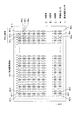
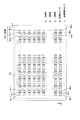
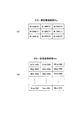
図5は有機ELパネル5の画素アレイでの画素及び光センサの配置を模式的に示している。方形で示すR画素、G画素、B画素は、それぞれ図2,図3で説明した画素回路10に相当する。
当該画素アレイでは、R画素、G画素、B画素の3つの画素によるユニットが、垂直方向にM個、水平方向にN個配設されているとする。
第1行目で第1列(ユニット単位の先頭列)のR画素、G画素、B画素を、画素R11,G11,B11とする。
第1行目で第N列(ユニット単位の最終列)のR画素、G画素、B画素を、画素R1N,G1N,B1Nとする。
第M行目(最終行)で第1列のR画素、G画素、B画素を、画素RM1,GM1,BM1とする。
第M行目で第N列のR画素、G画素、B画素を、画素RMN,GMN,BMNとする。
The correction coefficient setting process will be described with reference to FIGS.
First, the arrangement of pixels and photosensors will be described with reference to FIGS.
FIG. 5 schematically shows the arrangement of pixels and photosensors in the pixel array of the
In the pixel array, it is assumed that M units of three pixels of R pixel, G pixel, and B pixel are arranged in the vertical direction and N in the horizontal direction.
In the first row, the R pixel, G pixel, and B pixel in the first column (first column in unit unit) are designated as pixels R11, G11, and B11.
In the first row, the R pixel, G pixel, and B pixel in the Nth column (final column of unit unit) are defined as pixels R1 N , G1 N , and B1 N.
In the Mth row (final row), the R pixel, G pixel, and B pixel in the first column are designated as
The R pixel, G pixel, and B pixel in the Nth column in the Mth row are referred to as pixels R MN , G MN , and B MN .
但し、ここで破線で示す範囲AAが、有効画素領域であり、この有効画素領域AAに含まれる画素が、実際の表示に用いる有効画素である。
この例の場合、ユニット単位の最終列であるR画素(R1N〜RMN)、G画素(G1N〜GMN)、B画素(B1N〜BMN)は、有効画素領域AA外とされており、これがダミー画素とされる。
However, a range AA indicated by a broken line here is an effective pixel area, and pixels included in the effective pixel area AA are effective pixels used for actual display.
In this example, R pixels (R1 N to R MN ), G pixels (G1 N to G MN ), and B pixels (B1 N to B MN ), which are the last columns in unit units, are outside the effective pixel area AA. This is a dummy pixel.
本実施の形態では、上記のように例えばパワーオンの際などの補正係数設定処理を行うが、これは補正係数設定処理は、通常表示実行中にはできないためである。
一方、通常の表示動作実行中には、例えば一定時間間隔毎に、後述する補正係数更新処理を行う。これは通常の表示動作が長時間に及んでも、つまり、補正係数設定処理を行う機会がなかなか訪れなくても、適宜補正係数を修正していくことで、補正係数が画素劣化へ的確に対応した値となるようにする処理である。ダミー画素は、この通常の表示動作実行中の補正係数更新処理の際に用いる画素となる。
In the present embodiment, as described above, for example, correction coefficient setting processing at power-on or the like is performed, because the correction coefficient setting processing cannot be performed during normal display execution.
On the other hand, during normal display operation execution, correction coefficient update processing, which will be described later, is performed at regular time intervals, for example. This is because even if the normal display operation takes a long time, that is, even if there is no opportunity to perform the correction coefficient setting process, the correction coefficient can be appropriately dealt with by pixel correction by appropriately correcting the correction coefficient. It is a process to make it become the value. The dummy pixel is a pixel used in the correction coefficient update process during the normal display operation.
なお、表示動作実行中に行う補正係数更新処理については、第1,第2の補正係数更新処理として後述するが、第1の補正係数更新処理を採用する場合は、ダミー画素は、R、G、Bそれぞれについて最低1つあれば足りる。例えば画素R1N,G1N,B1Nをダミー画素として使用する。
しかしながら、パネル製造プロセス上の都合により、余分な他のダミー画素を含めて1列分のダミー画素を形成することはかまわない。
また、第1の補正係数更新処理の変形例や、第2の補正係数更新処理として、R、G、Bそれぞれについて複数のダミー画素を用いる例も述べる。
また図5の例では、ダミー画素はR、G、Bそれぞれの最終列の画素としたが、以上のことから、少なくとも1つ(R、G、Bで合計3つ)のダミー画素を形成する場合もあるし、ダミー画素の位置は有効画素領域AA外とする位置ならどこでも良い。例えば先頭列側、或いは先頭行又は最終行の画素としてもよい。
The correction coefficient update process performed during the execution of the display operation will be described later as the first and second correction coefficient update processes. However, when the first correction coefficient update process is employed, the dummy pixels are R, G , B is sufficient for each. For example, the pixels R1 N , G1 N and B1 N are used as dummy pixels.
However, for the convenience of the panel manufacturing process, one column of dummy pixels may be formed including other extra dummy pixels.
In addition, a modified example of the first correction coefficient update process and an example in which a plurality of dummy pixels are used for each of R, G, and B will be described as the second correction coefficient update process.
In the example of FIG. 5, the dummy pixels are the pixels in the final columns of R, G, and B. From the above, at least one (three in total, R, G, and B) dummy pixels are formed. In some cases, the position of the dummy pixel may be anywhere outside the effective pixel area AA. For example, it may be the pixel on the top column side, or the top row or the last row.
この図5のような画素アレイにおいて、○で示す画素補正センサが、上下の同色画素から等距離の位置に配置され、また、●で示す列補正センサが、第1行目の上側において、異なる列の同色画素から等距離の位置に配置されている。
なお、○で示す「画素補正センサ」と●で示す「列補正センサ」とは、説明の便宜上、区別しているにすぎず、同一の構造の光センサでよい。もちろん異なる構造であってもよい。
In the pixel array as shown in FIG. 5, the pixel correction sensors indicated by ◯ are arranged at equal distances from the upper and lower same color pixels, and the column correction sensors indicated by ● are different on the upper side of the first row. They are arranged at equidistant positions from the same color pixels in the column.
The “pixel correction sensor” indicated by ○ and the “column correction sensor” indicated by ● are merely distinguished for convenience of explanation, and may be optical sensors having the same structure. Of course, a different structure may be used.
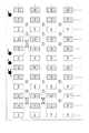
図6は、図5の一部として画素R11〜B43の範囲を拡大して示している。
列補正センサS01、S02、S03・・・、及び画素補正センサS11、S12、S13・・・が、図のように配設されている。
この例では、1つの画素補正センサは、2つの画素から等距離の位置に配置される。例えば画素補正センサS11は、画素R11,R21の中間位置とされる。また画素補正センサS21は、画素R21とR31の中間位置とされる。
即ち列方向に隣接する2つのR画素から等距離の位置に、それぞれ画素補正センサが配置されている。G画素の列、B画素の列についても同様である。
この画素補正センサは、上下に隣接する画素同士の間で相対的な発光輝度の差分を検出するものとされる。
FIG. 6 shows an enlarged range of the pixels R11 to B43 as a part of FIG.
The column correction sensors S01, S02, S03... And the pixel correction sensors S11, S12, S13.
In this example, one pixel correction sensor is disposed at a position equidistant from two pixels. For example, the pixel correction sensor S11 is an intermediate position between the pixels R11 and R21. Further, the pixel correction sensor S21 is set at an intermediate position between the pixels R21 and R31.
That is, pixel correction sensors are arranged at positions equidistant from two R pixels adjacent in the column direction. The same applies to the G pixel column and the B pixel column.
This pixel correction sensor detects a relative light emission luminance difference between vertically adjacent pixels.
また1つの列補正センサは、異なる列の2つの同色画素から等距離の位置に配置される。例えば列補正センサS01は、画素R11,R12から等距離の位置とされる。また画素補正センサS04は、画素R12とR13から等距離の位置とされる。
またG画素の列、B画素の列についても同様に列補正センサが設けられる。例えば列補正センサS02は、画素G11とG12から等距離の位置とされ、列補正センサS03は画素B11とB12から等距離の位置とされる。
この列補正センサは、異なる列の同色画素同士の間で相対的な発光輝度の差分を検出するものとされる。
One column correction sensor is arranged at a position equidistant from two identical color pixels in different columns. For example, the column correction sensor S01 is at a position equidistant from the pixels R11 and R12. Further, the pixel correction sensor S04 is located at an equal distance from the pixels R12 and R13.
Similarly, a column correction sensor is provided for the G pixel column and the B pixel column. For example, the column correction sensor S02 is positioned equidistant from the pixels G11 and G12, and the column correction sensor S03 is positioned equidistant from the pixels B11 and B12.
This column correction sensor detects a difference in relative emission luminance between pixels of the same color in different columns.
このような配置においては、画素補正センサから見れば、それぞれが2つの画素に対応することになる。例えば画素補正センサS11は、画素R11とR21の輝度検出用の光センサとなる。また画素補正センサS21は、画素R21とR31の輝度検出用の光センサとなる。
一方、画素側から見れば、第1行及び第M行以外の画素については、各画素に2つの画素補正センサが対応することになる。例えば画素R21から見れば、画素補正センサS11とS21が対応する。
第1行の各画素は、1つの画素補正センサと1つまたは2つの列補正センサが対応する。例えば画素R11から見れば、画素補正センサS11と列補正センサS01が対応する。また画素R12は、画素補正センサS14と列補正センサS01、S04が対応する。
In such an arrangement, each pixel corresponds to two pixels as viewed from the pixel correction sensor. For example, the pixel correction sensor S11 is an optical sensor for detecting the luminance of the pixels R11 and R21. The pixel correction sensor S21 is an optical sensor for detecting the luminance of the pixels R21 and R31.
On the other hand, when viewed from the pixel side, for pixels other than the first row and the Mth row, two pixel correction sensors correspond to each pixel. For example, when viewed from the pixel R21, the pixel correction sensors S11 and S21 correspond to each other.
Each pixel in the first row corresponds to one pixel correction sensor and one or two column correction sensors. For example, when viewed from the pixel R11, the pixel correction sensor S11 corresponds to the column correction sensor S01. The pixel R12 corresponds to the pixel correction sensor S14 and the column correction sensors S01 and S04.
このような対応関係は、特定の一つの基準画素(例えばR画素群については画素R11とする)を起点として、全ての画素(ダミー画素RMNまでの全R画素)が、光センサ(画素補正センサまたは列補正センサ)を介して橋渡しされているような状態を形成する。
G画素群、B画素群も同様である。例えばG画素群は、基準画素G11から、ダミー画素GMNまでの全G画素が、光センサで橋渡しされているような状態である。
ここで橋渡しという表現は単なる説明上のイメージである。具体的には、2つの画素が共通の光センサで輝度検出されていくことが、順次各光センサについて繰り返されることで、同色の全画素の、基準画素からみた相対的な発光輝度差分を、各光センサの検出ばらつきを排除して得られる構成であることを示している。
Such a correspondence relationship is that all pixels (all R pixels up to the dummy pixel R MN ) start from one specific reference pixel (for example, the pixel R11 for the R pixel group), and the optical sensor (pixel correction). A state of being bridged via a sensor or a column correction sensor).
The same applies to the G pixel group and the B pixel group. For example, the G pixel group is in a state in which all G pixels from the reference pixel G11 to the dummy pixel GMN are bridged by the optical sensor.
Here, the term “bridge” is merely an explanatory image. Specifically, the luminance detection of two pixels by a common optical sensor is sequentially repeated for each optical sensor, so that the relative emission luminance difference of all pixels of the same color as viewed from the reference pixel is It shows that the configuration is obtained by eliminating the detection variation of each optical sensor.
このように画素及び光センサ(画素補正センサと列補正センサ)を配設することで実現できる補正係数設定処理を説明する。 A correction coefficient setting process that can be realized by arranging pixels and photosensors (pixel correction sensor and column correction sensor) in this way will be described.
補正係数設定処理の概略は次の(1)〜(6)のとおりである。
(1)基準画素を基準表示データ信号値で点灯させ、その上または下の光センサで測定を行なう。基準画素はパネル内の任意の画素とする。基準表示データ信号値とは、或る特定の階調値である。全画素に基準表示データ信号値を与えて画素毎の発光輝度の差を検出するためである。また基準画素は、本例ではR画素群については画素R11とする。
例えば最初に、基準画素R11としての画素回路10に、基準表示データ信号値による信号電位Vsigを与えて発光させ、発光輝度を画素補正センサS11で検出する。
The outline of the correction coefficient setting process is as follows (1) to (6).
(1) A reference pixel is turned on with a reference display data signal value, and measurement is performed with an upper or lower light sensor. The reference pixel is an arbitrary pixel in the panel. The reference display data signal value is a specific gradation value. This is because a reference display data signal value is given to all the pixels to detect a difference in light emission luminance for each pixel. In this example, the reference pixel is the pixel R11 for the R pixel group.
For example, first, the
(2)当該検出を行った光センサに隣接する反対側の画素を基準表示データ信号で点灯させて測定を行なう。即ち、例えば次に、画素R21としての画素回路10に、基準表示データ信号値による信号電位Vsigを与えて発光させ、発光輝度を同じく画素補正センサS11で検出する。
(2) Measurement is performed by lighting the pixel on the opposite side adjacent to the photosensor that has performed the detection with the reference display data signal. That is, for example, next, the
(3)画素間の輝度差分から補正係数設定を行う。例えば上記(1)(2)により、画素R11,R21の輝度が、共通の画素補正センサS11で得られたことになる。そこで、その検出値から、基準画素R11に対する画素R21の検出値の差分(比)から、補正係数が算出できる。即ち、基準画素R11と同一の輝度で画素R21を発光させるようにするための補正値である。そして算出された補正係数を、画素R21についての補正係数として補正係数格納部6bに記憶する。
(3) A correction coefficient is set from the luminance difference between pixels. For example, according to the above (1) and (2), the luminance of the pixels R11 and R21 is obtained by the common pixel correction sensor S11. Therefore, the correction coefficient can be calculated from the difference (ratio) of the detection value of the pixel R21 with respect to the reference pixel R11 from the detection value. That is, this is a correction value for causing the pixel R21 to emit light with the same luminance as the reference pixel R11. Then, the calculated correction coefficient is stored in the correction
(4)次に、補正係数を更新した画素を基準にして、次の画素の補正係数を設定する。例えば先に補正係数を設定した画素R21を基準にして、画素R31の補正係数を設定する。このため、画素R21とR31の間で、上記(1)(2)(3)の処理を行う。
まず画素R21を基準表示データ信号値で発光させ、画素補正センサS21で発光輝度を検出する。但し、この場合は、画素R21に対しては、先に設定した補正係数による補正を行った基準表示データ信号値を与えることとなる。
次に、画素R31を基準表示データ信号値で発光させ、画素補正センサS21で発光輝度を検出する。
そして画素間の輝度差分から補正係数設定を行う。即ち画素R21,R31の輝度が、共通の画素補正センサS21で得られたことになるため、画素R21に対する画素R31の検出値の差分(比)から、補正係数を算出する。即ち、画素R21と同一の輝度で画素R31を発光させるようにするための補正値である。そして算出された補正係数を、画素R31についての補正係数として補正係数格納部6bに記憶する。ここで、画素R21については、先に設定した補正係数を反映させた基準表示データ信号値で発光させているため、今回求められた画素R31の補正係数は、基準画素R11と同一の輝度で画素R31を発光させるための補正値となる。
(4) Next, the correction coefficient of the next pixel is set with reference to the pixel with the updated correction coefficient. For example, the correction coefficient of the pixel R31 is set with reference to the pixel R21 for which the correction coefficient has been previously set. Therefore, the processes (1), (2), and (3) are performed between the pixels R21 and R31.
First, the pixel R21 is caused to emit light with the reference display data signal value, and the light emission luminance is detected by the pixel correction sensor S21. However, in this case, a reference display data signal value corrected by the previously set correction coefficient is given to the pixel R21.
Next, the pixel R31 is caused to emit light with the reference display data signal value, and the light emission luminance is detected by the pixel correction sensor S21.
Then, the correction coefficient is set from the luminance difference between pixels. That is, since the luminance of the pixels R21 and R31 is obtained by the common pixel correction sensor S21, the correction coefficient is calculated from the difference (ratio) of the detection value of the pixel R31 with respect to the pixel R21. That is, this is a correction value for causing the pixel R31 to emit light with the same luminance as the pixel R21. Then, the calculated correction coefficient is stored in the correction
(5)以下、列方向に順次同様の処理を行い、列方向の各画素(R41〜RM1)について、それぞれ補正係数を求め、補正係数格納部6bに記憶する。
(5) Thereafter, the same processing is sequentially performed in the column direction, and correction coefficients are obtained for the respective pixels (R41 to R M 1) in the column direction and stored in the correction
(6)次に、他の列の画素について補正係数設定を行う。例えば基準画素R11と画素R12の間で、列補正センサS01を用いて、上記(1)(2)(3)と同様の処理を行う。すると、画素R12について、基準画素R11と同一の輝度で画素R12を発光させるための補正係数を得ることができる。
画素R12の補正係数が設定できたら、次に画素R12とR22の間で、上記(4)の処理を行う。これにより、画素R22についても、基準画素R11と同一の輝度で画素R22を発光させるための補正係数を得ることができる。
以下、R32〜RM2についても同様の処理を繰りかえす。
(6) Next, correction coefficient setting is performed for pixels in other columns. For example, the same processing as (1), (2), and (3) is performed between the reference pixel R11 and the pixel R12 using the column correction sensor S01. Then, a correction coefficient for causing the pixel R12 to emit light with the same luminance as that of the reference pixel R11 can be obtained for the pixel R12.
After the correction coefficient for the pixel R12 has been set, the process (4) is performed between the pixels R12 and R22. As a result, a correction coefficient for causing the pixel R22 to emit light with the same luminance as that of the reference pixel R11 can also be obtained for the pixel R22.
Thereafter, the same processing is repeated for R32 to RM2.
以上のような処理を、ダミー画素RMNの補正係数設定まで行うことで、全R画素について、同一の表示データ信号が与えられたときに、基準画素R11と同一の輝度で発光させるための補正係数が得られたことになる。 By performing the above processing up to the setting of the correction coefficient of the dummy pixel RMN , when the same display data signal is given to all the R pixels, the correction is performed to emit light with the same luminance as that of the reference pixel R11. The coefficient is obtained.
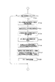
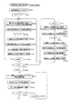
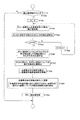
図4(a)のステップF102、または図4(b)のステップF202として、このようなR画素群についての補正係数設定処理を実現する信号処理部2の処理例を図7に示す。
まず信号処理部2は、ステップF300で補正係数格納部6bにおける全R画素についての補正係数をクリアする。次にステップF301で、処理対象の画素を指定する変数m,nについてm=1、n=1とする。
FIG. 7 shows a processing example of the signal processing unit 2 that realizes such correction coefficient setting processing for the R pixel group as Step F102 in FIG. 4A or Step F202 in FIG. 4B.
First, in step F300, the signal processing unit 2 clears correction coefficients for all R pixels in the correction
ステップF302では、信号処理部2は、画素Rmnについて、特定の階調値Xに相当する基準表示データ信号(以下「基準信号X」)を与えて発光させる。なお、このステップF302では、当該画素Rmnについて、補正係数格納部6bに記憶されている補正係数による補正を与える。但し、最初はm=1、n=1であり、画素Rmn=基準画素R11となり、また補正係数はクリアされている。従って、基準画素R11に対して、基準信号Xをそのまま与えることになる。具体的には、データドライバ4に基準信号Xを供給するとともに、ゲートドライバ3及びデータドライバ4に、画素R11の発光を指示する。
In step F302, the signal processing unit 2 causes the pixel Rmn to emit light by providing a reference display data signal (hereinafter referred to as “reference signal X”) corresponding to a specific gradation value X. In step F302, the pixel Rmn is corrected by the correction coefficient stored in the correction
ステップF303では、信号処理部2は、発光させた画素Rmnの下側の画素補正センサの検出値を、検出信号生成部7から取り込んで信号処理部2の内部で記憶する。この場合、基準画素R11の下側の画素補正センサS11の検出値を取り込むことになる。 In step F <b> 303, the signal processing unit 2 takes in the detection value of the pixel correction sensor on the lower side of the emitted pixel Rmn from the detection signal generation unit 7 and stores it in the signal processing unit 2. In this case, the detection value of the pixel correction sensor S11 below the reference pixel R11 is captured.
次に信号処理部2はステップF304で、変数mをインクリメントし、ステップF305で、画素Rmnについて、基準信号Xを与えて発光させる。なお、このステップF305は、データドライバ4に供給する基準信号Xについて補正は行わない。この場合、m=2とされているため、画素R21を基準信号Xで発光させることになる。
ステップF306では、信号処理部2は、発光させた画素Rmnの上側の画素補正センサの検出値を、検出信号生成部7から取り込んで信号処理部2の内部で記憶する。この場合、画素R21の上側の画素補正センサS11の検出値を取り込むことになる。つまり上記ステップF303と同一の画素補正センサS11の検出値である。
Next, in step F304, the signal processing unit 2 increments the variable m, and in step F305, gives the reference signal X to the pixel Rmn to emit light. In step F305, the reference signal X supplied to the data driver 4 is not corrected. In this case, since m = 2, the pixel R21 is caused to emit light with the reference signal X.
In step F <b> 306, the signal processing unit 2 takes in the detection value of the pixel correction sensor on the upper side of the emitted pixel Rmn from the detection signal generation unit 7 and stores it in the signal processing unit 2. In this case, the detection value of the pixel correction sensor S11 above the pixel R21 is captured. That is, the detection value of the pixel correction sensor S11 is the same as that in step F303.
信号処理部2は、ステップF307で、上記ステップF303及びF306で取り込んだ両検出値を用いて補正係数を算出する。即ちこの場合、両検出値とは、画素R11、R21について画素補正センサS11で検出した発光輝度の値である。
この両検出値の差分または比から、画素R21を、基準画素R11と同一の輝度で発光させるための補正係数を得ることができる。
そしてステップF308では、算出された補正係数を、画素R21についての補正係数として補正係数格納部6bに記憶する。
ここまでの処理で、基準画素R11を基準とした画素R21の補正係数が設定できたことになる。
In step F307, the signal processing unit 2 calculates a correction coefficient using both detection values acquired in steps F303 and F306. That is, in this case, both detection values are the values of the light emission luminance detected by the pixel correction sensor S11 for the pixels R11 and R21.
A correction coefficient for causing the pixel R21 to emit light with the same luminance as that of the reference pixel R11 can be obtained from the difference or ratio between the two detection values.
In step F308, the calculated correction coefficient is stored in the correction
With the processing so far, the correction coefficient of the pixel R21 with the reference pixel R11 as a reference can be set.
信号処理部2は、ステップF309で変数m=Mであるか否かを確認する。上述のように「M」は最終行の値である。つまりステップF309は、現在の列の最終行の画素まで、補正係数の設定が終えたか否かを確認する処理である。
上記のように画素R21の補正係数設定を行った時点では、まだ補正係数未設定の下方の画素が存在するため、ステップF302に戻る。
The signal processing unit 2 confirms whether or not the variable m = M in Step F309. As described above, “M” is the value of the last row. That is, step F309 is processing for confirming whether or not the correction coefficient has been set up to the pixels in the last row of the current column.
At the time when the correction coefficient of the pixel R21 is set as described above, there is still a lower pixel for which no correction coefficient is set, and the process returns to step F302.
この場合、ステップF302で信号処理部2は、画素Rmn(つまり画素R21)について、基準信号Xを与えて発光させる。このときは、当該画素Rmn(=R21)について、先に補正係数格納部6bに記憶させた補正係数による補正を与える。従って、この時点で画素R21は、基準画素R11と同じ発光輝度で発光していることになる。
そしてステップF303で信号処理部2は、発光させた画素Rmn(=R21)の下側の画素補正センサ、つまり今度は画素補正センサS21の検出値を、検出信号生成部7から取り込んで信号処理部2の内部で記憶する。
In this case, in step F302, the signal processing unit 2 causes the pixel Rmn (that is, the pixel R21) to emit light by providing the reference signal X. At this time, the pixel Rmn (= R21) is corrected using the correction coefficient stored in the correction
In step F303, the signal processing unit 2 takes in the detection value of the pixel correction sensor below the light-emitting pixel Rmn (= R21), that is, the pixel correction sensor S21 from the detection signal generation unit 7 to obtain a signal processing unit. 2 is stored inside.
次に信号処理部2はステップF304で、変数mをインクリメントし、ステップF305で、画素Rmnについて、基準信号X(無補正)を与えて発光させる。この場合、m=3とされているため、画素R31を基準信号Xで発光させることになる。
ステップF306では、信号処理部2は、発光させた画素Rmnの上側の画素補正センサの検出値を、検出信号生成部7から取り込んで信号処理部2の内部で記憶する。この場合、基準画素R31の上側の画素補正センサS21の検出値を取り込むことになる。つまり直前のステップF303と同一の画素補正センサS21の検出値である。
Next, in step F304, the signal processing unit 2 increments the variable m, and in step F305, gives a reference signal X (no correction) to the pixel Rmn to emit light. In this case, since m = 3, the pixel R31 is caused to emit light with the reference signal X.
In step F <b> 306, the signal processing unit 2 takes in the detection value of the pixel correction sensor on the upper side of the emitted pixel Rmn from the detection signal generation unit 7 and stores it in the signal processing unit 2. In this case, the detection value of the pixel correction sensor S21 above the reference pixel R31 is captured. That is, the detection value of the pixel correction sensor S21 is the same as that in step F303 just before.
信号処理部2は、ステップF307で、上記ステップF303及びF306で取り込んだ両検出値を用いて補正係数を算出する。即ちこの場合、両検出値とは、画素R21、R31について画素補正センサS21で検出した発光輝度の値である。
この両検出値の差分または比から、画素R31を、画素R21と同一の輝度(つまり基準画素R11と同一輝度)で発光させるための補正係数を得ることができる。
そしてステップF308では、算出された補正係数を、画素R31についての補正係数として補正係数格納部6bに記憶する。
In step F307, the signal processing unit 2 calculates a correction coefficient using both detection values acquired in steps F303 and F306. That is, in this case, both detection values are the values of the light emission luminance detected by the pixel correction sensor S21 for the pixels R21 and R31.
A correction coefficient for causing the pixel R31 to emit light with the same luminance as the pixel R21 (that is, the same luminance as the reference pixel R11) can be obtained from the difference or ratio between the two detection values.
In step F308, the calculated correction coefficient is stored in the correction
以上のステップF302〜F308の処理を、当該列の最終行の画素RM1の補正係数が設定されるまで繰り返していく。
そして画素RM1の補正係数が設定された直後のステップF309では、変数m=Mとなり、この場合、ステップF310に進んで、現在が最終列(第N列)の処理を終了したのか否かを確認する。即ち変数n=Nであるか否かを確認する。
The processes in steps F302 to F308 are repeated until the correction coefficient for the pixel R M1 in the last row of the column is set.
Then, in step F309 immediately after the correction coefficient of the
上記のように第1列のR画素(R11〜RM1)までの補正係数設定を終えた時点では、第2列以降のR画素が残っている。この時点で変数n=1であって、NではないためステップF311に進む。
信号処理部2は、まず変数mの値をm=1とする。そしてステップF312で画素Rmn(つまりこの場合、基準画素R11)について、基準信号Xを与えて発光させる。ステップF312にでは、先に画素Rmnについて補正係数格納部6bに記憶させた補正係数による補正を与えるが、基準画素R11の場合に限っては、実質的に補正はない。例えば補正値を乗算係数とした場合は、基準画素R11についての補正係数=1(加減算値とした場合は補正値=0)であるためである。
そしてステップF313で信号処理部2は、発光させた画素Rmn(=基準画素R11)に対応する列補正センサ、この場合、列補正センサS01の検出値を、検出信号生成部7から取り込んで信号処理部2の内部で記憶する。
As described above, when the correction coefficient setting for the R pixels (R11 to R M 1) in the first column is completed, the R pixels in the second column and thereafter remain. At this time, since the variable n = 1 and not N, the process proceeds to step F311.
The signal processing unit 2 first sets the value of the variable m to m = 1. In step F312, the pixel Rmn (that is, the reference pixel R11 in this case) is supplied with the reference signal X to emit light. In step F312, correction is performed using the correction coefficient stored in the correction
In step F313, the signal processing unit 2 takes in the detection value of the column correction sensor corresponding to the emitted pixel Rmn (= reference pixel R11), in this case, the column correction sensor S01, from the detection signal generation unit 7, and performs signal processing. Store inside the unit 2.
次に信号処理部2はステップF314で、変数nをインクリメントし、ステップF315で、画素Rmn(この場合画素R12)について、基準信号X(無補正)を与えて発光させる。
ステップF316では信号処理部2は、発光させた画素Rmn(=R12)に対応する列補正センサ、この場合、列補正センサS01の検出値を、検出信号生成部7から取り込んで信号処理部2の内部で記憶する。つまり直前のステップF313と同一の列補正センサの検出値である。
Next, in step F314, the signal processing unit 2 increments the variable n, and in step F315, the signal processing unit 2 gives the reference signal X (no correction) to the pixel Rmn (in this case, the pixel R12) to emit light.
In step F316, the signal processing unit 2 fetches the detection value of the column correction sensor corresponding to the emitted pixel Rmn (= R12), in this case, the column correction sensor S01, from the detection signal generation unit 7, and the signal processing unit 2 Memorize internally. That is, it is the detection value of the same column correction sensor as in the immediately preceding step F313.
信号処理部2は、ステップF317で、上記ステップF313及びF316で取り込んだ両検出値を用いて補正係数を算出する。即ちこの場合、両検出値とは、基準画素R11、R12について列補正センサS01で検出した発光輝度の値である。
この両検出値の差分または比から、画素R12を、基準画素R11と同一の輝度で発光させるための補正係数を得ることができる。
そしてステップF318では、算出された補正係数を、画素R12についての補正係数として補正係数格納部6bに記憶する。
In step F317, the signal processing unit 2 calculates a correction coefficient using both detection values acquired in steps F313 and F316. That is, in this case, the both detection values are values of the light emission luminance detected by the column correction sensor S01 for the reference pixels R11 and R12.
A correction coefficient for causing the pixel R12 to emit light with the same luminance as that of the reference pixel R11 can be obtained from the difference or ratio between the two detection values.
In step F318, the calculated correction coefficient is stored in the correction
そしてステップF302に進む。R画素群としての2列目の先頭の画素R12について補正係数が設定されたため、以降、ステップF302〜F308を、当該2列目の各画素について実行することになる。
即ちまず画素R12を、補正係数で補正した基準信号Xで発光させて画素補正センサS14で輝度検出を行う(F302,F303)。次に画素R22を無補正の基準信号Xで発光させて画素補正センサS14で輝度検出を行う(F304,F305,F306)。そして、両検出値から、画素R22を、画素R21と同一の輝度(つまり基準画素R11と同一輝度)で発光させるための補正係数を得、算出された補正係数を、画素R22についての補正係数として補正係数格納部6bに記憶する(F307,F308)。
Then, the process proceeds to Step F302. Since the correction coefficient is set for the first pixel R12 in the second column as the R pixel group, Steps F302 to F308 are subsequently executed for each pixel in the second column.
That is, first, the pixel R12 is caused to emit light with the reference signal X corrected with the correction coefficient, and the luminance detection is performed by the pixel correction sensor S14 (F302, F303). Next, the pixel R22 is caused to emit light with an uncorrected reference signal X, and the luminance detection is performed by the pixel correction sensor S14 (F304, F305, F306). Then, a correction coefficient for causing the pixel R22 to emit light with the same luminance as the pixel R21 (that is, the same luminance as the reference pixel R11) is obtained from both detection values, and the calculated correction coefficient is used as the correction coefficient for the pixel R22. It memorize | stores in the correction
以降、順次、画素R22,R32、画素R32とR34・・・とステップF302〜F308の処理を行い、最終行の画素RM2まで補正係数を設定する。
すると今度は、画素R12とR13の関係で列補正センサS04を用いてステップF311〜F318の処理を行い、その後、ステップF302〜F308で、R画素群としての第3列目の画素(画素R13〜RM3)までの補正係数設定を行う。
このような処理を繰り返し、最終行、最終列のダミー画素RMNの設定が終わった時点で、ステップF310で変数n=Nとなり、R画素群の全画素に対する補正係数設定が終了する。
Thereafter, sequentially, the pixel R22, R32, performs processing of the pixel R32 and R34 · · · and the step F302~F308, sets the correction coefficient to the pixel R M 2 of the last line.
Then, this time, the processing of steps F311 to F318 is performed using the column correction sensor S04 in relation to the pixels R12 and R13, and then the pixels in the third column (pixels R13 to The correction coefficient is set up to RM3).
Such processing is repeated, and when the setting of the dummy pixel R MN in the last row and the last column is completed, the variable n becomes N in step F310, and the correction coefficient setting for all the pixels in the R pixel group is completed.
補正係数設定処理は、以上で完了するわけであるが、ステップF319〜F321では、後述する通常の表示動作実行中の補正係数更新処理のために必要な処理を行う。
信号処理部2はステップF319では、或るダミー画素(例えばダミー画素R1N)を基準信号Xで発光させる。この場合、基準信号Xはダミー画素R1Nについて設定した補正係数で補正してからデータドライバ4に与える。
ステップF320では、特定の光センサでダミー画素R1Nの発光輝度の検出値を取り込む。特定の光センサとは、後述する補正係数更新処理で同じくダミー画素R1Nの発光輝度を検出する光センサである。例えば図5の場合、ダミー画素R1Nの直下の画素補正センサとすればよい。どの光センサをここでいう特定の光センサとして決めておくかは任意であり、例えばとなりのダミー画素G1Nの直下の画素補正センサや、或いはダミー画素G1Nの右上の列補正センサを、特定の光センサと決めても良い。
なお、補正係数更新処理でダミー画素R1Nの発光輝度を検出するときは、有効画素領域AAは通常に表示を行っているため、有効画素の発光の影響を受けないようにすることが適切である。そのためには、特定の光センサは、なるべく有効画素領域AAから離れていることが望ましい。その意味では、ダミー画素R1Nの直下の画素補正センサより、ダミー画素G1N或いはB1Nの直下の画素補正センサが適しているとも言える。
信号処理部2はステップF321で、特定の光センサの検出値を、ダミー画素R1Nの測定値としてダミー測定値格納部6aに格納する。
The correction coefficient setting process is completed as described above. In steps F319 to F321, processes necessary for a correction coefficient update process during execution of a normal display operation described later are performed.
In step F319, the signal processing unit 2 causes a certain dummy pixel (for example, dummy pixel R1 N ) to emit light with the reference signal X. In this case, the reference signal X is corrected by the correction coefficient set for the dummy pixel R1 N and then given to the data driver 4.
In Step F320, the detection value of the emission luminance of the dummy pixel R1 N is captured by the specific photosensor. The specific optical sensor is an optical sensor that similarly detects the light emission luminance of the dummy pixel R1 N in a correction coefficient update process described later. For example, in the case of FIG. 5, a pixel correction sensor just below the dummy pixel R1 N may be used. Which the light sensor is optional or is determined in advance as a particular light sensor mentioned here, for example, pixel correction sensor immediately below the dummy pixel G1 N next, or the upper right column correction sensors of the dummy pixel G1 N, specific It may be determined that the optical sensor.
When detecting the light emission luminance of the dummy pixel R1 N in the correction coefficient update process, it is appropriate to prevent the effective pixel area AA from being affected by the light emission of the effective pixel because the effective pixel area AA is normally displayed. is there. For this purpose, it is desirable that the specific photosensor is as far away from the effective pixel area AA as possible. In that sense, it can be said that the pixel correction sensor immediately below the dummy pixel G1 N or B1 N is more suitable than the pixel correction sensor immediately below the dummy pixel R1 N.
The signal processing unit 2 in step F321, the detected value of the particular optical sensor is stored in the dummy measurement
G画素群については図4のステップF103またはF203で、B画素群については図4のステップF104またはF204で、図7と同様の処理が行われる。即ち図7における画素R11〜RMNを、G画素群については画素G11〜GMN、B画素群については画素B11〜BMNとして考え、またそれぞれ対応する光センサを用いればよい。 For the G pixel group, the same processing as in FIG. 7 is performed in step F103 or F203 in FIG. 4, and for the B pixel group in step F104 or F204 in FIG. That pixel R11~R MN in FIG 7, the pixel G11~G MN for G pixel group, considered as a pixel B11~B MN for B pixel groups, also may be used a light sensor respectively corresponding.
このような処理を行うことにより、補正係数更新対象とする全画素(少なくとも有効表示領域の全画素)について、補正係数が設定されることになる。
特にパワーオン時、またはパワーオフ時に補正係数更新が行われることで、経時劣化にも対応して適切な補正係数が補正係数格納部6に格納されるように適宜更新されることになる。
その上で、本例の場合、各画素の補正係数は基準画素R11から順次、共通の光センサでの輝度検出値に基づいて算出される。これは、補正係数算出の際に、各光センサの検出ばらつきの影響を受けないことを意味する。
従って補正係数は、各光センサの検出ばらつきの影響を排除した適切な値となる。
これらによって本例の表示装置1は、輝度ムラのない高品質な画面表示を行うことができる。
By performing such processing, correction coefficients are set for all pixels (at least all pixels in the effective display area) that are correction coefficient update targets.
In particular, when the correction coefficient is updated at the time of power-on or power-off, an appropriate correction coefficient is appropriately updated so as to be stored in the correction
In addition, in the case of this example, the correction coefficient of each pixel is calculated sequentially from the reference pixel R11 based on the luminance detection value of the common photosensor. This means that the calculation of the correction coefficient is not affected by the detection variation of each optical sensor.
Therefore, the correction coefficient is an appropriate value excluding the influence of the detection variation of each optical sensor.
Accordingly, the
またダミー画素も含めて、適切な補正係数設定が行われることになるが、これは後述する表示動作実行中にダミー画素を用いて行う補正係数更新処理を精度良く実行するという点で好適となる。 In addition, appropriate correction coefficient setting including dummy pixels is performed, which is preferable in that correction coefficient update processing performed using dummy pixels during execution of the display operation described later is performed with high accuracy. .
なお、以上の図7のような補正係数設定処理を実現するための光センサ配置例は、他にも考えられる。
例えば列補正センサは、第1行目の上側ではなく、第m行目の下側において、異なる列の同色画素から等距離の位置に配置されていてもよいし、配置が可能であれば、途中の行の間に配置されていても良い。あくまでも、或る列の1つの画素と、異なる列の1つの同色画素とから等距離の位置に設けられて、異なる列の画素同士で共通に発光輝度を検出できるようにすればよい。
It should be noted that other optical sensor arrangement examples for realizing the correction coefficient setting process as shown in FIG. 7 are also conceivable.
For example, the column correction sensor may be arranged at the same distance from the same color pixel in different columns on the lower side of the m-th row, not on the upper side of the first row. It may be arranged between the rows. To the last, it is only necessary to be provided at a position equidistant from one pixel in a certain column and one same color pixel in a different column so that the light emission luminance can be detected in common between the pixels in different columns.
また、図7の処理では列方向の画素について補正係数設定を行った後、列補正センサを介して次の列の補正に進むようにしたが、先に第1行目の全R画素について補正を行い、その後、各列で、画素補正センサを介して、順次列方向に並ぶR画素の補正係数設定を行うようにすることもできる。もちろん他の順序も考えられ、どのような順序で各画素の補正係数設定を行うかは、全く任意である。 In the processing of FIG. 7, the correction coefficient is set for the pixels in the column direction, and then the process proceeds to the correction of the next column via the column correction sensor. After that, it is also possible to perform correction coefficient setting for R pixels sequentially arranged in the column direction in each column via the pixel correction sensor. Of course, other orders are possible, and the order in which the correction coefficient is set for each pixel is completely arbitrary.
また、補正係数設定処理の例は図7に限られず、光センサの配置も多様な例が考えられる。いずれにしても、2以上の画素が共通の光センサによって輝度検出され、基準とする画素に対して相対的に同一輝度の発光を行うための補正係数を設定することを、順次連鎖的に全ての画素に行われるようにすればよい。すると、個々の光センサの検出ばらつきを排除して、画面上の1の基準画素と同様の発光輝度を全画素で得られるようになる。
このような補正係数設定を行うためには、光センサの配置が、全画素について上述の橋渡し状態を形成していればよい。
Further, the example of the correction coefficient setting process is not limited to FIG. 7, and various examples of the arrangement of the optical sensors are conceivable. In any case, all of the two or more pixels are sequentially detected in a chain by sequentially detecting the luminance by a common photosensor and setting a correction coefficient for emitting light having the same luminance relative to the reference pixel. This may be performed on the pixels. Then, the detection variation of the individual optical sensors is eliminated, and the same emission luminance as that of one reference pixel on the screen can be obtained for all the pixels.
In order to perform such correction coefficient setting, the arrangement of the photosensors only needs to form the above-described bridging state for all pixels.
例えば図8,図9に示すような光センサの配置例も考えられる。画素の配置は上述した図5,図6と同様である。
図8に示すように、画素アレイ内において、○で示す画素補正センサが配置される。最外周の画素の周囲には、先に述べた列補正センサは無く、この例では、○で示す画素補正センサが列補正センサとしての機能も果たす。
For example, arrangement examples of optical sensors as shown in FIGS. 8 and 9 are also conceivable. The arrangement of the pixels is the same as that shown in FIGS.
As shown in FIG. 8, a pixel correction sensor indicated by ◯ is arranged in the pixel array. There is no column correction sensor described above around the outermost pixel, and in this example, the pixel correction sensor indicated by ◯ also functions as a column correction sensor.
図9に拡大して示すが、各画素補正センサは、4つの同色画素から等距離の位置に配置されている。
例えば画素補正センサS11は、画素R11,R21,R12,R22からそれぞれ等距離の位置とされる。また画素補正センサS21は、画素R21,R31,R22,R32からそれぞれ等距離の位置とされる。G画素群、B画素群についても同様である。
この画素補正センサは、対応する4つの画素同士の間で相対的な発光輝度の差分を検出するものとされる。
このような光センサの配置も、特定の一つの基準画素(例えばR画素群については画素R11)を起点として、全ての画素(画素RMNまでの全R画素)が、光センサ(画素補正センサ)を介して橋渡しされているような状態を形成する。
この場合、上記図7と同様の処理でもよいし、1つの光センサに対応する4つの画素を1つのブロックとしてブロックごとに順次補正係数設定を行っていくこともできる。
そしてこのセンサ配置例の場合、1つの画素補正センサで4つの画素の相関で補正係数を算出するため、より精度の高い補正係数が得られる。
Although enlarged in FIG. 9, each pixel correction sensor is arranged at a position equidistant from four identical color pixels.
For example, the pixel correction sensor S11 is positioned equidistant from the pixels R11, R21, R12, and R22. In addition, the pixel correction sensor S21 is positioned equidistant from the pixels R21, R31, R22, and R32. The same applies to the G pixel group and the B pixel group.
This pixel correction sensor detects a relative light emission luminance difference between four corresponding pixels.
Also this arrangement of the optical sensor, starting from the particular one of the reference pixel (for example, the pixel R11 for R pixel group), all the pixels (all R pixels to the pixel R MN), an optical sensor (pixel correction sensor ) Form a state of being bridged through.
In this case, the same processing as in FIG. 7 may be performed, and correction coefficients may be sequentially set for each block with four pixels corresponding to one photosensor as one block.
In the case of this sensor arrangement example, the correction coefficient is calculated by the correlation of the four pixels by one pixel correction sensor, so that a correction coefficient with higher accuracy can be obtained.
また、図10、図11のような光センサ配置例も考えられる。
図10に示すように、画素アレイ内において、○で示す画素補正センサ及び●で示す列補正センサが配置される。
図11に拡大して示すが、各画素補正センサは、4つの同色画素から等距離の位置に配置されている。
例えば画素補正センサS11は、画素R11,R21,R12,R22からそれぞれ等距離の位置とされる。また画素補正センサS21は、画素R21,R31,R22,R32からそれぞれ等距離の位置とされる。
列補正センサは、隣接する同色の最上段のブロックにおける画素同士から等距離の位置に配置される。
例えば列補正センサS01は、画素R11,R21,R12,R22のブロックと、このブロックに隣接する画素R13,R23,R14,R24のブロックとを橋渡しするものとして、画素R12と画素R13から等距離の位置に配置される。
G画素群、B画素群についても同様である。
Moreover, the example of optical sensor arrangement | positioning like FIG. 10, FIG. 11 is also considered.
As shown in FIG. 10, a pixel correction sensor indicated by ◯ and a column correction sensor indicated by ● are arranged in the pixel array.
As shown in an enlarged view in FIG. 11, each pixel correction sensor is arranged at a position equidistant from four identical color pixels.
For example, the pixel correction sensor S11 is positioned equidistant from the pixels R11, R21, R12, and R22. In addition, the pixel correction sensor S21 is positioned equidistant from the pixels R21, R31, R22, and R32.
The column correction sensor is arranged at a position equidistant from the pixels in the adjacent uppermost block of the same color.
For example, the column correction sensor S01 bridges a block of pixels R11, R21, R12, and R22 and a block of pixels R13, R23, R14, and R24 adjacent to the block, and is equidistant from the pixels R12 and R13. Placed in position.
The same applies to the G pixel group and the B pixel group.
このような光センサの配置も、特定の一つの基準画素(例えばR画素群については画素R11)を起点として、全ての画素(画素RMNまでの全R画素)が、光センサ(画素補正センサまたは列補正センサ)を介して橋渡しされているような状態を形成する。
従って、上記図7のような処理や、1つの画素補正センサに対応する4つの画素を1つのブロックとしてブロックごとに順次補正係数設定を行っていく処理を行うことで、全画素について各光センサの検出ばらつきを排除した補正係数設定を行うことができる。
またこの例では、光センサの数を大幅に削減できるという利点が得られる。
Also this arrangement of the optical sensor, starting from the particular one of the reference pixel (for example, the pixel R11 for R pixel group), all the pixels (all R pixels to the pixel R MN), an optical sensor (pixel correction sensor Alternatively, a state of being bridged via a column correction sensor) is formed.
Therefore, by performing the processing as shown in FIG. 7 or the processing for sequentially setting the correction coefficient for each block with four pixels corresponding to one pixel correction sensor as one block, each photosensor It is possible to set a correction coefficient that eliminates the detection variation.
Moreover, in this example, the advantage that the number of optical sensors can be reduced significantly is acquired.
また光センサの削減という観点からは、図12のように、画素補正センサを、R、G、B各色の画素で共用することも考えられる。
つまりこの場合、各画素補正センサは、或る色の2つの同色発光画素に対して等距離であり、かつ、他の色の2つの同色発光画素に対しても等距離である位置に配置されている。
例えば画素補正センサS11は、画素R11,R21から等距離で、かつ画素G11、G21から等距離で、かつ画素B11,B21から等距離の位置となる。
また画素補正センサS21は、画素R21,R31から等距離で、かつ画素G21、G31から等距離で、かつ画素B21,B31から等距離の位置となる。
列補正センサについては共用していない。即ち画素R11,R12に対して列補正センサS01が等距離に配置され、画素G11,G12に対して列補正センサS02が等距離に配置され、画素B11,B12に対して列補正センサS03が等距離に配置される。
このように画素補正センサを各色で共用できるように配置することでも、図7のような処理は可能であり、その上で、光センサの数を大幅に削減できる。
From the viewpoint of reducing the number of photosensors, it is also conceivable that the pixel correction sensor is shared by R, G, and B pixels as shown in FIG.
That is, in this case, each pixel correction sensor is arranged at a position that is equidistant with respect to two same-color light emitting pixels of a certain color and is also equidistant with respect to two same-color light emitting pixels of another color. ing.
For example, the pixel correction sensor S11 is equidistant from the pixels R11 and R21, equidistant from the pixels G11 and G21, and equidistant from the pixels B11 and B21.
In addition, the pixel correction sensor S21 is equidistant from the pixels R21 and R31, equidistant from the pixels G21 and G31, and equidistant from the pixels B21 and B31.
The column correction sensor is not shared. That is, the column correction sensor S01 is arranged at an equal distance with respect to the pixels R11 and R12, the column correction sensor S02 is arranged at an equal distance with respect to the pixels G11 and G12, and the column correction sensor S03 is equal to the pixels B11 and B12. Placed at a distance.
Thus, by arranging the pixel correction sensors so that they can be shared by the respective colors, the processing as shown in FIG. 7 can be performed, and the number of photosensors can be greatly reduced.
[4.通常の表示動作実行中の処理]
以上の補正係数設定処理を例えばパワーオンの際などに行うことで、経時劣化にも対応して適切な補正係数を設定し、画面上の輝度ムラを低減できる。
ところが表示装置1が、長時間、表示を継続するような使用をされる場合、補正係数設定処理を行う機会がなかなか訪れないこととなる。そして長時間表示動作が継続することで、その間に画素毎に劣化の進行が異なり、画面上の輝度ムラが生じてくることもある。発光輝度の劣化の進行は表示輝度によって異なり、表示実行中は各画素が映像内容によって異なる輝度で発光しているためである。このことは、画素毎の補正係数が、長時間の表示継続によって、適切でなくなっていくことを意味する。
[4. Processing during normal display operation]
By performing the above correction coefficient setting process at the time of power-on, for example, it is possible to set an appropriate correction coefficient corresponding to deterioration with time and reduce luminance unevenness on the screen.
However, when the
そこで本実施の形態では、表示実行中でも、例えば一定時間毎に、各画素の補正係数を修正する補正係数更新処理を行うようにしている。
ここではまず、一定時間毎の補正係数更新処理に至るまでの、通常の表示動作実行中の処理について説明する。
Therefore, in the present embodiment, even during display execution, for example, correction coefficient update processing for correcting the correction coefficient of each pixel is performed at regular intervals.
Here, first, a description will be given of a process during execution of a normal display operation until a correction coefficient update process is performed every predetermined time.
まず図13で、メモリ部6の記憶内容を示しておく。
ダミー測定値格納部6aには、R、G、Bの各ダミー画素(例えばR1N,G1N,B1N)について、上記図7のステップF319〜F321で記憶した発光輝度の測定値R−DM、G−DM、B−DMが格納される。
補正係数格納部6bには、上記図7のステップF300〜F310で設定した、各画素毎の補正係数が記憶される。即ちR画素群について補正係数CR11〜CRMN、G画素群について補正係数CG11〜CGMN、B画素群について補正係数CB11〜CBMNが記憶される。
First, FIG. 13 shows the storage contents of the
In the dummy measurement
The correction
画素信号積算値格納部6cには、以下に述べる表示動作実行中の処理で、各有効画素の表示データ信号値を積算した積算値が記憶されていくことになる。即ちR画素群について積算値QR11〜QRM(N-1)、G画素群について積算値QG11〜QGM(N-1)、B画素群について積算値QB11〜QBM(N-1)である。
In the pixel signal integrated
図14(a)で通常の表示動作実行中の信号処理部2の処理を示す。
信号処理部2には、毎フレームで各画素の表示データ信号が入力されるが、ステップF601では、各画素の表示データ信号値を、その時点で画素信号積算値格納部6cに記憶されている値に加算して更新する。
例えば画素R11について入力された表示データ信号値を「DR11」とすると、画素R11についての積算値QR11を、
QR11=QR11+DR11
として更新する。他の全有効画素についても同様に積算して画素信号積算値格納部6cの記憶値を更新する。
FIG. 14A shows processing of the signal processing unit 2 during normal display operation execution.
The display data signal of each pixel is input to the signal processing unit 2 every frame. In step F601, the display data signal value of each pixel is stored in the pixel signal integrated
For example, if the display data signal value input for the pixel R11 is “D R11 ”, the integrated value Q R11 for the pixel R11 is
Q R11 = Q R11 + D R11
Update as. All other effective pixels are similarly integrated to update the stored value of the pixel signal integrated
そしてステップF602では、各画素についての表示データ信号値を、補正係数格納部6bに記憶されている補正係数を用いて補正し、データドライバ4に供給する。
なお、このとき、ダミー画素については表示データ信号値は入力されないが、信号処理部2はダミー画素(R1N〜RMN、G1N〜GMN、B1N〜BMN)に対する表示データ信号を生成し、補正係数格納部6bに格納されているこれらの画素の補正係数を用いて補正してデータドライバ4に供給する。即ちダミー画素も発光駆動する。但し、後述する図15の処理で使用するダミー画素R1N(及びG1N、B1N)以外は、全く発光させなくてもよい。
ダミー画素に与える表示データ信号値は、有効画素領域AA内の画素に対する表示データ信号値をそのまま用いればよい。例えば隣接する列の画素(R1(N-1)〜RM(N-1)、G1(N-1)〜GM(N-1)、B1(N-1)〜BM(N-1))の表示データ信号値を、ダミー画素(R1N〜RMN、G1N〜GMN、B1N〜BMN)の表示データ信号値として用い、補正してデータドライバ4に供給する。もちろん他の画素(例えば画面中央付近の画素)の表示データ信号値をダミー画素用として流用してもよい。
In step F602, the display data signal value for each pixel is corrected using the correction coefficient stored in the correction
At this time, no display data signal value is input to the dummy pixels, but the signal processing unit 2 generates display data signals for the dummy pixels (R1 N to R MN , G1 N to G MN , B1 N to B MN ). Then, correction is performed using the correction coefficients of these pixels stored in the correction
As the display data signal value given to the dummy pixel, the display data signal value for the pixels in the effective pixel area AA may be used as it is. For example, adjacent columns of pixels (R1 (N-1) to RM (N-1) , G1 (N-1) to GM (N-1) , B1 (N-1) to BM (N-1 ) ) Are used as display data signal values for the dummy pixels (R1 N to R MN , G1 N to G MN , B1 N to B MN ), and are supplied to the data driver 4 after correction. Of course, display data signal values of other pixels (for example, pixels near the center of the screen) may be used as dummy pixels.
以上のステップF601,F602の処理を、通常表示動作の終了と判断されるまで(F603)、フレーム毎に繰り返す。
従って、フレーム単位の表示データ信号が入力されるたびに、信号処理部2は画素信号積算値格納部6cの値を積算更新していき、またダミー画素を含めて全画素について、補正係数を用いて補正した状態で表示駆動させるようにする。
The processes in steps F601 and F602 described above are repeated for each frame until it is determined that the normal display operation is finished (F603).
Therefore, each time a display data signal in units of frames is input, the signal processing unit 2 integrates and updates the value of the pixel signal integrated
ステップF601で更新する画素信号積算値格納部6cの積算値は、後述する補正係数更新処理の際に各画素の劣化の進行度合いを推定する情報となる。劣化の進行度合いは、表示輝度によって異なるが、各表示データ信号値(発光させる階調値)を積算していけば、その平均値として、補正係数更新処理を実行するまでの期間の平均的な輝度階調を求めることができるためである。
またステップF602で、ダミー画素についても発光させるのは、ダミー画素にも表示内容に応じた劣化を発生させるためである。
The integrated value of the pixel signal integrated
In step F602, the dummy pixels are caused to emit light in order to cause the dummy pixels to deteriorate depending on the display contents.
なお、画素信号積算値格納部6cの積算値は、毎フレーム更新していくことが望ましいが、すると、積算値の値が大きくなり、画素信号積算値格納部6cとしての記憶容量が多大となる。そこで、記憶容量が制限される場合などは、適度な間隔で積算値更新を行うようにしても良い。例えば1分に1回、5分に1回などである。
図14(b)に、その場合の処理例を示す。
信号処理部2はステップF650で、例えば5分に1回などの積算タイミングに至ったか否かを判定する。積算タイミングでなければステップF652に進み、現在のフレームの表示データ信号については、補正処理を行って補正後の表示データ信号(ダミー画素も含む)をデータドライバ4に供給する。
一方、積算タイミングとなった場合は、そのフレームの表示データ信号については、ステップF651で、画素信号積算値格納部6cの積算値の更新を行い、ステップF652で補正処理を行って補正後の表示データ信号(ダミー画素も含む)をデータドライバ4に供給する。これをステップF653で表示終了とされるまで繰り返す。
It should be noted that the integrated value of the pixel signal integrated
FIG. 14B shows a processing example in that case.
In step F650, the signal processing unit 2 determines whether or not an integration timing such as once every 5 minutes has been reached. If it is not the integration timing, the process proceeds to step F652, and the display data signal of the current frame is corrected, and the corrected display data signal (including dummy pixels) is supplied to the data driver 4.
On the other hand, when the integration timing is reached, the display data signal of the frame is updated in step F651, the integration value in the pixel signal
[5.第1の補正係数更新処理例]
通常の表示動作実行中は、以上の図14(a)又は(b)の処理を行いながら、所定期間毎に補正係数を修正する補正係数更新処理を行う。例えば30分間隔、1時間間隔、5時間間隔、10時間間隔などの所定期間間隔で補正係数更新処理を行う。
補正係数更新処理のタイミングとなったときに信号処理部2が実行する補正係数更新処理の例を図15に示す。なお図15は1つの色(例えばR画素群)についての処理を示している。G画素群、B画素群についても同様の処理を行うことになる。
[5. First correction coefficient update processing example]
While the normal display operation is being executed, the correction coefficient update process for correcting the correction coefficient is performed every predetermined period while performing the process of FIG. For example, the correction coefficient update process is performed at predetermined time intervals such as 30 minutes, 1 hour, 5 hours, and 10 hours.
FIG. 15 shows an example of the correction coefficient update process executed by the signal processing unit 2 when the correction coefficient update process timing comes. FIG. 15 shows processing for one color (for example, R pixel group). The same processing is performed for the G pixel group and the B pixel group.
補正係数更新処理のタイミングとなったら、信号処理部2は図15のステップF701からF702に進み、補正係数更新処理を開始する。
なお、通常の表示動作は実行してるため、図14の処理と並行して図15の処理を行うことになる。但し、図15の補正係数更新処理を実行する間は、図14(a)のステップF602(又は図14(b)のステップF652)では、ダミー画素に対する処理は行わない。図15の処理で例えばダミー画素R1Nを使用し、また他の使用しないダミー画素はダミー画素R1Nの輝度測定に影響を与えないようにするため、発光させないようにする必要があるためである。
When the timing of the correction coefficient update process is reached, the signal processing unit 2 proceeds from step F701 to F702 in FIG. 15 and starts the correction coefficient update process.
Since the normal display operation is executed, the process of FIG. 15 is performed in parallel with the process of FIG. However, while the correction coefficient update process of FIG. 15 is executed, the process for the dummy pixel is not performed in step F602 of FIG. 14A (or step F652 of FIG. 14B). This is because, for example, the dummy pixel R1 N is used in the process of FIG. 15, and other unused dummy pixels need not be emitted in order not to affect the luminance measurement of the dummy pixel R1 N. .
図15のステップF702では、ダミー画素(例えばR1N)を、基準信号Xで発光させる。図14の処理により、毎フレームでダミー画素を含めて表示データ信号値による発光をさせているが、この補正係数更新処理を行うときは、ダミー画素についてはダミー画素R1Nのみを、固定の階調値である基準信号Xを与えるようにする(他のダミー画素は発光させない)。
そしてステップF703で、信号処理部2は、検出信号生成部7からダミー画素R1Nに対応する特定の光センサの検出値を取り込む。特定の光センサとは、図7のステップF320で用いた特定の光センサと同一の光センサである。
In step F702 of FIG. 15, a dummy pixel (for example, R1 N ) is caused to emit light with the reference signal X. In the process of FIG. 14, the light is emitted by the display data signal value including the dummy pixel in each frame. When this correction coefficient update process is performed, only the dummy pixel R1 N is fixed to the fixed pixel for the dummy pixel. A reference signal X that is a tone value is provided (other dummy pixels are not allowed to emit light).
In step F <b> 703, the signal processing unit 2 takes in a detection value of a specific photosensor corresponding to the dummy pixel R <b> 1 N from the detection signal generation unit 7. The specific optical sensor is the same optical sensor as the specific optical sensor used in step F320 in FIG.
ステップF704では、前回の検出値と、今回の検出値(直前のステップF703で得た検出値)から、ダミー画素R1Nについての発光輝度の変化量(即ち通常は劣化量)を判定する。
前回の検出値とは、その時点でダミー測定値格納部6aに記憶されている測定値R−DM(図13参照)である。このステップF704では、前回と今回の発光輝度の検出値(測定値)を比較して、その差分を劣化量とする。
そしてステップF704で信号処理部2は、劣化量から補正係数修正値を算出する。この補正係数修正値は、補正係数格納部6bの現在のダミー画素R1Nについての補正係数CR1Nを修正する値である。
劣化が生じている場合は、その劣化分に相当するだけ補正係数を修正すれば、前回と同一の輝度で発光させることができる。そこで基準信号Xに対する前回と今回の発光輝度の差分(=劣化量)又はその比に相当する補正係数修正値を求める。
この補正係数修正値は、補正係数について発光輝度劣化を補償する値となる。
In step F704, the amount of change in light emission luminance (ie, usually the amount of deterioration) for the dummy pixel R1 N is determined from the previous detection value and the current detection value (the detection value obtained in the previous step F703).
The previous detection value is the measurement value R-DM (see FIG. 13) stored in the dummy measurement
In step F704, the signal processing unit 2 calculates a correction coefficient correction value from the deterioration amount. This correction coefficient correction value is a value for correcting the correction coefficient C R1N for the current dummy pixel R1 N in the correction
If deterioration occurs, light can be emitted with the same luminance as the previous time by correcting the correction coefficient corresponding to the deterioration. Therefore, a correction coefficient correction value corresponding to the difference (= deterioration amount) or the ratio between the previous and current emission luminances with respect to the reference signal X is obtained.
The correction coefficient correction value is a value that compensates for the emission luminance deterioration of the correction coefficient.
しかしながら、ここで求めた補正係数修正値は、あくまでダミー画素R1Nについての値である。
有効画素領域AAの各画素は、それぞれ毎フレーム毎に多様な階調で発光しており、全ての画素がダミー画素R1Nと同様に劣化が進行しているわけではない。
そこで、各有効画素の劣化を推定して、補正係数修正値を調整する処理を行う。
However, the correction coefficient correction value obtained here is a value for the dummy pixel R1 N to the last.
Each pixel in the effective pixel area AA emits light with various gradations for each frame, and not all the pixels are deteriorated similarly to the dummy pixel R1 N.
Therefore, processing for estimating the deterioration of each effective pixel and adjusting the correction coefficient correction value is performed.
ステップF706で信号処理部2は、各画素の平均信号値を算出する。即ちその時点で画素信号積算値格納部6cに記憶されている各R画素の積算値(QR11〜QRM(N-1))から、各R画素の平均信号値(AVQR11〜AVQRM(N-1))を求める。
なお、このとき、画素信号積算値格納部6cの各値(QR11〜QRM(N-1))として、平均信号値(AVQR11〜AVQRM(N-1))の値に書き換える。今回の図15の処理が終了した後の図14の処理での最初の積算値とするためである。
そしてステップF707では、各R画素について平均信号値(AVQR11〜AVQRM(N-1))を元に、所定の関数を用いて補正係数修正値を調整する。
In step F706, the signal processing unit 2 calculates an average signal value of each pixel. That is, the average signal value (AVQ R11 to AVQ RM ( AVQ R11 to AVQ RM ( ) of each R pixel is calculated from the integrated value (Q R11 to Q RM (N-1) ) of each R pixel stored in the pixel signal integrated
At this time, as the values of the pixel signal integrated value storing unit 6c (Q R11 ~Q RM (N -1)), rewrites the value of the average signal value (AVQ R11 ~AVQ RM (N- 1)). This is because the first integrated value in the process of FIG. 14 after the process of FIG.
In step F707, the correction coefficient correction value is adjusted using a predetermined function based on the average signal value (AVQ R11 to AVQ RM (N-1) ) for each R pixel.
ステップF704で求めた補正係数修正値は基準信号Xについて測定した値に基づく。
或るR画素の平均信号値が基準信号Xとほぼ同じであれば、その画素については補正係数修正値はそのまま用いればよい。
一方、或るR画素の平均信号値が基準信号Xより大きければ、それだけ画素劣化の進行度合いが大きいと推定できる。
また、或るR画素の平均信号値が基準信号Xより小さければ、それだけ画素劣化の進行度合いが小さいと推定できる。
平均信号値と基準信号Xとの差に応じて、所定の関数演算(一次関数又は二次関数)を用いて補正係数修正値を調整することで、このような劣化度合いに応じた画素毎の補正係数修正値を得ることができる。
The correction coefficient correction value obtained in step F704 is based on the value measured for the reference signal X.
If the average signal value of a certain R pixel is substantially the same as the reference signal X, the correction coefficient correction value may be used as it is for that pixel.
On the other hand, if the average signal value of a certain R pixel is larger than the reference signal X, it can be estimated that the degree of progress of pixel degradation is that much.
Further, if the average signal value of a certain R pixel is smaller than the reference signal X, it can be estimated that the degree of progress of pixel degradation is small.
Depending on the difference between the average signal value and the reference signal X, the correction coefficient correction value is adjusted using a predetermined function calculation (a linear function or a quadratic function), so that each pixel corresponding to such a degree of deterioration is adjusted. A correction coefficient correction value can be obtained.
即ち発光輝度劣化に応じた補正係数の修正とは、表示データ信号値を高く補正する方向に補正係数を修正するものであるが、例えば劣化進行度合いが大きい画素については、補正係数を修正するための補正係数修正値の値が高くなり、劣化進行度合いが小さい画素については、補正係数を修正するための補正係数修正値の値が低くなるようにする。 In other words, correction of the correction coefficient according to light emission luminance deterioration is to correct the correction coefficient in the direction of correcting the display data signal value higher. For example, for a pixel having a large degree of deterioration, the correction coefficient is corrected. The correction coefficient correction value for correcting the correction coefficient is set to be low for pixels with a high correction coefficient correction value and a small degree of deterioration progression.
このように画素に応じて補正係数修正値を調整したうえで、その調整後の補正係数修正値を用いて補正係数格納部6bにおける各R画素の補正係数を修正更新する。
例えばステップF705でダミー画素R1Nの検出値から求めた補正係数修正値を「rC」とし、各R画素毎に平均信号値(AVQR11〜AVQRM(N-1))に応じて調整した各画素の補正係数修正値を「rCR11」〜「rCRM(N-1)」とすると、
例えば補正係数格納部6bの補正係数CR11〜CRM(N-1)について、
CR11=CR11+rCR11 (又はCR11=CR11×rCR11)
CR21=CR21+rCR21 (又はCR21=CR21×rCR21)
CRM(N-1)=CRM(N-1)+rCRM(N-1) (又はCRM(N-1)=CRM(N-1)×rCRM(N-1))
といように補正係数CR11〜CRM(N-1)を修正更新していく。なお上記括弧内は、補正係数修正値を比の値で求めた場合である。
Thus, after adjusting the correction coefficient correction value according to the pixel, the correction coefficient correction value of each R pixel in the correction
For example, the correction coefficient correction value obtained from the detection value of the dummy pixel R1 N in step F705 is “rC”, and each R pixel is adjusted according to the average signal value (AVQ R11 to AVQ RM (N−1) ). When the correction coefficient correction value of the pixel is “rCR 11 ” to “rCR RM (N−1) ”,
For example, for the correction coefficients C R11 to C RM (N-1) in the correction
C R11 = C R11 + rC R11 (or C R11 = C R11 × rC R11 )
C R21 = C R21 + rC R21 (or C R21 = C R21 × rC R21 )
CRM (N-1) = CRM (N-1) + rCRM (N-1) (or CRM (N-1) = CRM (N-1) * rCRM (N-1) )
Thus, the correction coefficients C R11 to C RM (N-1) are corrected and updated. In the parentheses, the correction coefficient correction value is obtained as a ratio value.
なお、ダミー画素R1Nの補正係数CR1Nについては、
CR1N=CR1N+rC (又はCR1N=CR1N×rC)
とすればよい。
For the correction coefficient C R1N of the dummy pixel R1 N ,
C R1N = C R1N + rC (or C R1N = C R1N × rC)
And it is sufficient.
ステップF707で以上のように補正係数の修正を行ったら、ステップF708で、ダミー測定値格納部6aの測定値R−DMを、今回ステップF703で取り込んだ検出値に更新する。次回の図15の補正係数更新処理で、前回の検出値として用いるためである。
そして図15の処理を終える。
このような図15の処理を、G画素群、B画素群についても同様に行う。
When the correction coefficient is corrected as described above in step F707, in step F708, the measurement value R-DM in the dummy measurement
Then, the process of FIG. 15 is finished.
Such processing of FIG. 15 is similarly performed for the G pixel group and the B pixel group.
以上のように通常の表示動作実行中にも、例えば定期的に補正係数更新処理が行われることで、長時間継続表示を行っていても、適宜、補正係数が適切な値に修正されていくことになる。このため、例えパワーオンの際などの補正係数設定処理が長時間行われない場合でも、所定時間毎に図15の処理が行われて補正係数が最適化され、画面上の輝度ムラの発生を低減又は解消できる。
またパワーオンの際等の補正係数設定処理では、ダミー画素も含めて光センサの検出ばらつきを排除した精度の高い補正係数設定が行われているため、表示動作実行中のダミー画素を用いた補正係数更新処理の精度も高いものとなる。
As described above, even during normal display operation execution, for example, correction coefficient update processing is periodically performed, so that the correction coefficient is appropriately corrected to an appropriate value even if continuous display is performed for a long time. It will be. Therefore, even when the correction coefficient setting process is not performed for a long time, such as when the power is turned on, the process shown in FIG. 15 is performed every predetermined time to optimize the correction coefficient, thereby causing uneven brightness on the screen. Can be reduced or eliminated.
In addition, in the correction coefficient setting process at the time of power-on, etc., the correction coefficient setting with high accuracy that excludes the detection variation of the optical sensor including the dummy pixel is performed, so the correction using the dummy pixel during execution of the display operation is performed. The accuracy of the coefficient update process is also high.
なお、以上の図15の処理では、ダミー画素R1Nについて、基準信号Xのみで発光輝度変化(劣化量)を測定し、補正係数修正値を得た。そして、各画素の平均信号値で補正係数修正値を関数演算により調整し、その後、各画素について調整した補正係数修正値を用いて補正係数の修正を行った。
ここで、各画素について補正係数修正値を調整するための関数は、予め設定した固定の関数、即ち補正係数修正値と、劣化推定量の関係をリニアもしくはノンリニアに規定する関数であればよい。
しかし、必ずしも常に固定の関数が適切とは限らない。そこで、より精密に補正係数の修正を行うためには、複数の基準信号(例えば3つの異なる階調値の基準信号X、Y、Zを用いる手法も考えられる。
In the process of FIG. 15 described above, the change in emission luminance (deterioration amount) is measured for the dummy pixel R1 N using only the reference signal X, and the correction coefficient correction value is obtained. Then, the correction coefficient correction value is adjusted by function calculation using the average signal value of each pixel, and then the correction coefficient is corrected using the correction coefficient correction value adjusted for each pixel.
Here, the function for adjusting the correction coefficient correction value for each pixel may be a fixed function set in advance, that is, a function that prescribes the relationship between the correction coefficient correction value and the estimated deterioration amount linearly or non-linearly.
However, a fixed function is not always appropriate. Therefore, in order to correct the correction coefficient more precisely, a method using a plurality of reference signals (for example, reference signals X, Y, and Z having three different gradation values) can be considered.
例えばダミー画素R1Nについて、基準信号X,Y,Zでそれぞれ発光輝度を測定する。そして基準信号X,Y,Zでそれぞれ前回の測定値と比較して、各階調X,Y,Zでの発光輝度の変化量(劣化量)を判定する。
なおこのため、ダミー測定値格納部6aには、図16(a)のように、ダミー画素R1Nについて、各基準信号X、Y、Zによる前回の測定値R−DM(X)、R−DM(Y)、R−DM(Z)を格納するようにして、今回の各検出値と比較する。ダミー画素G1N、B1Nついても同様である。
For example, with respect to the dummy pixel R1 N , the emission luminance is measured with reference signals X, Y, and Z, respectively. Then, the reference signals X, Y, and Z are compared with the previous measurement values, respectively, and the change amount (deterioration amount) of the light emission luminance at each gradation X, Y, and Z is determined.
For this reason, as shown in FIG. 16A, the dummy
例えば3点(3つの階調値)で劣化量を検出することで、階調値に対する劣化量の関数カーブを求めることができる。
すると、その関数を用い、各画素の平均信号値に応じて補正係数修正値を調整すれば、より各画素についての補正係数修正を的確に算出でき、ひいては、各画素の補正係数を的確に修正できることになる。
もちろん2つの階調値の基準信号X、Yで実行したり、或いは4以上の階調値の各基準信号で実行してもよい。
For example, by detecting the deterioration amount at three points (three gradation values), a function curve of the deterioration amount with respect to the gradation value can be obtained.
Then, if the correction coefficient correction value is adjusted according to the average signal value of each pixel using the function, the correction coefficient correction for each pixel can be calculated more accurately, and the correction coefficient for each pixel is corrected accordingly. It will be possible.
Of course, it may be executed with reference signals X and Y having two gradation values, or may be executed with reference signals having four or more gradation values.
[6.第2の補正係数更新処理例]
第2の補正係数更新処理を説明する。この処理は、多数のダミー画素を用いる。そして、上記のように処理過程で、各画素の平均信号値で補正係数修正値を調整するわけであるが、そのときに関数演算を用いず、適切に各画素に対応した補正係数修正値を得ることができるようにするものである。
[6. Second correction coefficient update processing example]
The second correction coefficient update process will be described. This process uses a large number of dummy pixels. In the process as described above, the correction coefficient correction value is adjusted by the average signal value of each pixel. At that time, the correction coefficient correction value corresponding to each pixel is appropriately set without using the function calculation. It is something that can be obtained.
図5に示したように、R画素群についてはダミー画素R1N〜RMNのM個のダミー画素が存在する。このため、最大M個のダミー画素を利用することができる。
本例ではダミー画素R1N〜RMNを全て利用する例を挙げる。
ダミー測定値格納部6aについては図16(b)に示すように、ダミー画素R1N〜RMNに対応して測定値R1N−DM〜RMN−DMを記憶するようにする。G画素群のダミー画素G1N〜GMN、B画素群のダミー画素B1N〜BMNについても同様である。即ち測定値G1N−DM〜GMN−DM、測定値B1N−DM〜BMN−DMを記憶する。
As shown in FIG. 5, for the R pixel group, there are M dummy pixels of dummy pixels R1 N to R MN . For this reason, a maximum of M dummy pixels can be used.
In this example, an example in which all the dummy pixels R1 N to R MN are used is given.
The dummy
また、パワーオンの際のR画素群に対する補正係数設定処理は図17のようにする。図17は、ステップF300〜F310までは上記図7と同様であるが、ステップF330〜F335として、図16(b)のダミー測定値格納部6aにダミー画素R1N〜RMNに対応する測定値R1N−DM〜RMN−DMを記憶する処理を行う。
Further, the correction coefficient setting process for the R pixel group at power-on is as shown in FIG. 17, step F300~F310 Until is similar to FIG. 7, in step F330~F335, dummy measurement
即ちステップF310までの処理が終了したら、ステップF320で変数m=1とし、ダミー画素R1Nを指定する状態とする。
信号処理部2はステップF321では、ダミー画素R1Nを基準信号Xで発光させる。この場合、基準信号Xはダミー画素R1Nについて設定した補正係数で補正してからデータドライバ4に与える。
ステップF332では、特定の光センサでダミー画素R1Nの発光輝度の検出値を取り込む。そしてステップF333で、特定の光センサの検出値を、ダミー画素R1Nの測定値R1N−DMとしてダミー測定値格納部6aに格納する。
この処理を、ステップF334で変数m=Mと判断されるまで、ステップF335で変数mをインクリメントしながら繰り返す。
これによってダミー画素R1N〜RMNに対応する測定値R1N−DM〜RMN−DMがダミー測定値格納部6aに記憶される。
G画素群、B画素群についても、この図17と同様に補正係数設定処理を行う。
That is, when the processing up to step F310 is completed, the variable m = 1 is set in step F320, and the dummy pixel R1 N is designated.
In step F321, the signal processing unit 2 causes the dummy pixel R1 N to emit light with the reference signal X. In this case, the reference signal X is corrected by the correction coefficient set for the dummy pixel R1 N and then given to the data driver 4.
In Step F332, the detection value of the emission luminance of the dummy pixel R1 N is captured by the specific photosensor. In step F333, the detection value of the specific photosensor is stored in the dummy
This process is repeated while incrementing the variable m in step F335 until it is determined in step F334 that the variable m = M.
As a result, the measurement values R1 N -DM to R MN -DM corresponding to the dummy pixels R1 N to R MN are stored in the dummy
The correction coefficient setting process is performed for the G pixel group and the B pixel group as in FIG.
通常の表示動作実行中には、信号処理部2は図14(a)又は(b)の処理を行う。
但し、図14(a)のステップF602(又は図14(b)のステップF652)では、ダミー画素R1N〜RMNに対する発光駆動は、それぞれ特定の階調値で毎フレーム発光させる処理となる。
例えば階調数とダミー画素数Mに応じて、各ダミー画素R1N〜RMNに与える表示データ信号値(階調値)を設定しておく。
例えばダミー画素R1Nには最小階調値、ダミー画素RMNには最大階調値とし、ダミー画素R2N〜R(M-1)Nまでは、最小階調値から最大階調値の間を例えば等間隔に振り分けた各階調値の表示データ信号を与えるようにする。もちろん必ずしも等間隔でなくても良い。これにより、ダミー画素R1Nは最小階調値で常時発光し、ダミー画素R2Nは次の階調値で常時発光し、・・・ダミー画素RMNは最大階調値で常時発光するという状態となる。
During normal display operation execution, the signal processing unit 2 performs the processing of FIG.
However, in step F602 of FIG. 14A (or step F652 of FIG. 14B), the light emission driving for the dummy pixels R1 N to R MN is a process of emitting light for each frame with a specific gradation value.
For example, display data signal values (gradation values) to be given to the respective dummy pixels R1 N to R MN are set according to the number of gradations and the number of dummy pixels M.
For example, the dummy pixel R1 N has a minimum gradation value, the dummy pixel R MN has a maximum gradation value, and the dummy pixels R2 N to R (M-1) N are between the minimum gradation value and the maximum gradation value. For example, a display data signal of each gradation value distributed at equal intervals is provided. Of course, it does not necessarily have to be equally spaced. State that this makes the dummy pixel R1 N emits always at the minimum gradation value, the dummy pixel R2 N emits always at the next gray scale value, ... dummy pixel R MN emits light constantly at the maximum tone value It becomes.
補正値更新タイミングとなったら、補正係数更新処理として図18の処理を行う。
即ち信号処理部2は、補正係数更新処理のタイミングとなったら図18のステップF750からF751に進み、補正係数更新処理を開始する。
なお、通常の表示動作は実行してるため、図14の処理と並行して図18の処理を行うことになる。但し、図18の補正係数更新処理を実行する間は、図14(a)のステップF602(又は図14(b)のステップF652)では、ダミー画素R1N〜RMNに対する上記のようなそれぞれ固定の階調値での発光駆動は中止する。
When the correction value update timing comes, the process of FIG. 18 is performed as the correction coefficient update process.
That is, the signal processing unit 2 proceeds from Step F750 to F751 in FIG. 18 when the correction coefficient update process timing comes, and starts the correction coefficient update process.
Since the normal display operation is executed, the process of FIG. 18 is performed in parallel with the process of FIG. However, while performing correction coefficient update process of FIG. 18, in each above-mentioned for the dummy pixel R1 N to R MN fixed (step F652 or FIG 14 (b)) Step F602 shown in FIG. 14 (a) The light emission driving at the gradation value is stopped.
信号処理部2はステップF751では変数m=1とし、ステップF752で、ダミー画素Rmn(つまりR1N)を、基準信号Xで発光させる。
そしてステップF753で信号処理部2は、検出信号生成部7からダミー画素R1Nに対応する特定の光センサの検出値を取り込む。特定の光センサとは、図17のステップF332でダミー画素R1Nについて用いた特定の光センサと同一の光センサである。
The signal processing unit 2 sets the variable m = 1 in step F751, and causes the dummy pixel Rmn (that is, R1 N ) to emit light with the reference signal X in step F752.
In step F753, the signal processing unit 2 takes in the detection value of the specific photosensor corresponding to the dummy pixel R1 N from the detection signal generation unit 7. The specific optical sensor is the same optical sensor as the specific optical sensor used for the dummy pixel R1 N in step F332 of FIG.
そしてステップF754で変数m=Mとなるまで、ステップF755で変数mをインクリメントしながら、ステップF752,F753の処理を繰り返す。
従って、各ダミー画素R1N〜RMNについて、それぞれ基準信号Xで発光させた輝度の検出値が、それぞれ図17のステップF322で用いたのと同一の光センサによって取り込まれることになる。
Then, the process of steps F752 and F753 is repeated while incrementing the variable m in step F755 until the variable m = M in step F754.
Accordingly, for each dummy pixel R1 N to R MN , the detected luminance value emitted by the reference signal X is captured by the same optical sensor used in step F322 of FIG.
各ダミー画素R1N〜RMNについて今回の検出値を得たら、信号処理部2はステップF756に進み、前回の検出値と、今回の検出値から、ダミー画素R1N〜RMNのそれぞれについての発光輝度の変化量(即ち通常は劣化量)を判定する。
前回の検出値とは、その時点でダミー測定値格納部6aに記憶されている測定値R1N−DM〜RMN−DM(図16(b)参照)である。このステップF756では、各ダミー画素R1N〜RMNについて前回と今回の発光輝度の検出値(測定値)を比較して、その差分を劣化量とする。
つまり各ダミー画素R1N〜RMNについてそれぞれ劣化量を求める。
そしてステップF757で信号処理部2は、各ダミー画素R1N〜RMNの劣化量から各ダミー画素R1N〜RMNの補正係数修正値を算出する。
When the current detection value is obtained for each of the dummy pixels R1 N to R MN , the signal processing unit 2 proceeds to Step F756, and the dummy pixel R1 N to R MN is determined from the previous detection value and the current detection value. A change amount of light emission luminance (that is, a normal deterioration amount) is determined.
The previous detection values are measurement values R1 N -DM to R MN -DM (see FIG. 16B) stored in the dummy measurement
That is, the deterioration amount is obtained for each of the dummy pixels R1 N to R MN .
The signal processing unit 2 in step F757 calculates a correction coefficient modification values of the dummy pixel R1 N to R MN from degradation amount of the dummy pixel R1 N to R MN.
続いてステップF758,F759では、補正係数修正値を各画素の劣化推定に応じて補正係数修正値を調整した上で、各画素の補正係数を修正する。
まずステップF758で信号処理部2は、各画素の平均信号値を算出する。即ちその時点で画素信号積算値格納部6cに記憶されている各R画素の積算値(QR11〜QRM(N-1))から、各R画素の平均信号値(AVQR11〜AVQRM(N-1))を求める。
なお、このとき、画素信号積算値格納部6cの各値(QR11〜QRM(N-1))として、平均信号値(AVQR11〜AVQRM(N-1))の値に書き換える。今回の図18の処理が終了した後の図14の処理での最初の積算値とするためである。
そしてステップF759では、各R画素について平均信号値(AVQR11〜AVQRM(N-1))を元に、補正係数修正値を調整したうえ、補正係数修正値を用いて各画素の補正係数を修正する。
Subsequently, in steps F758 and F759, the correction coefficient correction value is adjusted according to the deterioration estimation of each pixel, and then the correction coefficient of each pixel is corrected.
First, in step F758, the signal processing unit 2 calculates an average signal value of each pixel. That is, the average signal value (AVQ R11 to AVQ RM ( AVQ R11 to AVQ RM ( ) of each R pixel is calculated from the integrated value (Q R11 to Q RM (N-1) ) of each R pixel stored in the pixel signal integrated
At this time, as the values of the pixel signal integrated value storing unit 6c (Q R11 ~Q RM (N -1)), rewrites the value of the average signal value (AVQ R11 ~AVQ RM (N- 1)). This is because the first integrated value in the process of FIG. 14 after the process of FIG.
In step F759, the correction coefficient correction value is adjusted based on the average signal value (AVQ R11 to AVQ RM (N-1) ) for each R pixel, and the correction coefficient of each pixel is calculated using the correction coefficient correction value. Correct it.
ここで、各ダミー画素R1N〜RMNは、通常の表示動作実行中に、それぞれ異なる固定の階調値で発光させている。
従って、ステップF757で求めた各ダミー画素R1N〜RMNの補正係数修正値は、各階調値での劣化度合いに応じた値となっている。
例えばダミー画素R1Nについての補正係数修正値は、最小階調値で常時発光させた場合の劣化に応じた値となっている。またダミー画素RMNについての補正係数修正値は最大階調値で常時発光させた場合の劣化に応じた値となっている。
つまり、各ダミー画素R1N〜RMNについての各補正係数修正値として、各種の平均信号値に対応する補正係数修正値が得られていることになる。
従って、各画素の補正係数修正値は、その平均信号値と一致又は近い階調値で発光させていたダミー画素の補正係数修正値を用いればよい。例えば平均信号値が最大階調値に近い画素は、ダミー画素R1Nとほぼ同様の劣化進行具合であると推定でき、また平均信号値が階調値L1に近い画素は、階調値L1もしくはそれに近い階調値で発光させていたダミー画素とほぼ同様の劣化進行具合であると推定できるためである。
Here, each of the dummy pixels R1 N to R MN emits light with different fixed gradation values during execution of the normal display operation.
Therefore, the correction coefficient correction values of the dummy pixels R1 N to R MN obtained in step F757 are values corresponding to the degree of deterioration at each gradation value.
For example, the correction coefficient correction value for the dummy pixel R1 N is a value corresponding to deterioration when the light is always emitted with the minimum gradation value. Further, the correction coefficient correction value for the dummy pixel R MN is a value corresponding to deterioration when the light is always emitted with the maximum gradation value.
That is, correction coefficient correction values corresponding to various average signal values are obtained as the correction coefficient correction values for the dummy pixels R1 N to R MN .
Accordingly, the correction coefficient correction value for each pixel may be the correction coefficient correction value for the dummy pixel that has been emitted with a gradation value that matches or is close to the average signal value. For example, a pixel whose average signal value is close to the maximum gradation value can be estimated to have substantially the same degree of deterioration as the dummy pixel R1 N, and a pixel whose average signal value is close to the gradation value L1 is the gradation value L1 or This is because it can be estimated that the deterioration progress is almost the same as that of the dummy pixel that emits light with a gradation value close to that.
そこで、各画素の補正係数修正値の調整として、関数演算で行うのではなく、画素の平均信号値に近い階調値で発光させていたダミー画素を選択し、そのダミー画素についての補正係数修正値を、その画素の補正係数修正値とする。このような対応付けを全画素について行い、各画素の補正係数修正値とする。
このように各有効画素に応じて補正係数修正値を調整(この場合、選択)したうえで、その補正係数修正値を用いて補正係数格納部6bにおける各R画素の補正係数を修正更新する。
ダミー画素R1N〜RMNについては、それぞれ自身の画素について求めた補正係数修正値を用いて補正係数を修正すればよい。
Therefore, to adjust the correction coefficient correction value for each pixel, select a dummy pixel that emits light with a gradation value close to the average signal value of the pixel, rather than using function calculation, and correct the correction coefficient for that dummy pixel. The value is the correction coefficient correction value for that pixel. Such association is performed for all the pixels, and the correction coefficient correction value for each pixel is used.
In this way, after adjusting (selecting in this case) the correction coefficient correction value according to each effective pixel, the correction coefficient of each R pixel in the correction
For the dummy pixels R1 N to R MN , the correction coefficient may be corrected using the correction coefficient correction value obtained for each pixel.
ステップF759で以上のように補正係数の修正を行ったら、ステップF760で、ダミー測定値格納部6aの測定値R1N−DM〜RMN−DMを、今回ステップF753で取り込んだ各ダミー画素R1N〜RMNの検出値に更新する。次回の図18の補正係数更新処理で、前回の検出値として用いるためである。
そして図18の処理を終える。
このような図18の処理を、G画素群、B画素群についても同様に行う。
When the correction coefficient is corrected as described above in step F759, in step F760, the measured values R1 N -DM to R MN -DM in the dummy measured
Then, the process of FIG. 18 is finished.
18 is similarly performed for the G pixel group and the B pixel group.
以上の処理によっても、通常の表示動作実行中に例えば定期的に補正係数更新処理が行われることになるため、長時間継続表示を行っていても、適宜、補正係数が適切な値に修正されていく。このため、例えパワーオンの際などの補正係数設定処理が長時間行われない場合でも、所定時間毎に図18の処理が行われて補正係数が最適化され、画面上の輝度ムラの発生を低減又は解消できる。
Even with the above processing, the correction coefficient update processing is performed periodically, for example, during normal display operation execution. Therefore, even if continuous display is performed for a long time, the correction coefficient is appropriately corrected to an appropriate value. To go. Therefore, even when the correction coefficient setting process is not performed for a long time, such as when the power is turned on, the process shown in FIG. 18 is performed every predetermined time to optimize the correction coefficient, thereby causing uneven brightness on the screen. Can be reduced or eliminated.
[7.変形例]
以下、各種の変形例を述べる。
図15,図18のような補正係数更新処理は一定時間間隔でなくてもよい。例えば何らかの手法で全体的な劣化の進行具合を認識して、或る程度の発光輝度劣化が生じていることが推定される場合を補正係数更新処理のタイミングとしても良い。
例えば上記図18の第2の補正係数更新処理のように、通常表示動作時に、ダミー画素にそれぞれ固定の階調値を与える場合、その間に光センサで輝度を適時に測定していくことで、劣化の進行の程度が推定可能である。従って、劣化の進行が或る程度あることを検出した時点で、補正係数更新処理を行うということも考えられる。
また、ユーザの操作等によって補正係数更新処理を開始するようにしてもよい。
[7. Modified example]
Various modifications will be described below.
The correction coefficient update processing as shown in FIGS. 15 and 18 may not be at regular time intervals. For example, the correction coefficient update process may be performed when it is estimated that a certain degree of light emission luminance deterioration has occurred by recognizing the progress of overall deterioration by some method.
For example, as in the second correction coefficient updating process of FIG. 18 described above, when a fixed gradation value is given to each dummy pixel during normal display operation, the luminance is measured with a photosensor in the meantime, The degree of progress of deterioration can be estimated. Accordingly, it is conceivable that the correction coefficient update process is performed when it is detected that the deterioration has progressed to some extent.
Further, the correction coefficient update process may be started by a user operation or the like.
また図7のような補正係数設定処理についても、システムの起動時、終了時以外にも、ユーザの操作に応じて、一旦通常の表示動作を停止して実行するようにしてもよい。 In addition, the correction coefficient setting process as shown in FIG. 7 may be temporarily stopped and executed in response to a user operation, other than when the system is started or ended.
また上記図15の第1の補正係数更新処理では、R画素群については1つのダミー画素R1Nのみというように、1つのダミー画素を用いているが、ダミー画素R1N〜RMNのM個のダミー画素を利用することも考えられる。
例えばその場合、図17,図18で述べたように各ダミー画素について発光輝度の測定を行い、その各ダミー画素についての測定値の平均値を、前回の平均測定値と比較して補正係数修正値を求めるというように、図15の処理を変形してもよい。
In the first correction coefficient updating process of FIG. 15 described above, one dummy pixel is used such that only one dummy pixel R1 N is used for the R pixel group, but M pixels of the dummy pixels R1 N to R MN are used. It is possible to use the dummy pixels.
For example, in this case, as described in FIGS. 17 and 18, the emission luminance is measured for each dummy pixel, and the average value of the measured values for each dummy pixel is compared with the previous average measured value to correct the correction coefficient. The process of FIG. 15 may be modified such that a value is obtained.
また、パワーオンの際等に行う図7のような補正係数設定処理については、画面全体の画素について順次、補正係数設定を行っていくため、比較的時間を要する。
この処理時間を短縮するには、例えば画面上を複数の領域に分け、領域毎に並行して図7の処理を行うことが考えられる。但し、各領域での基準画素については、先に相関をとって、補正係数を設定しておくことが必要である。例えば第1行目の画素のみ先に補正係数を設定し、その後、2つの領域で、第1行目の或る画素を基準画素として用いて並行処理を行うようにすればよい。
Further, the correction coefficient setting process as shown in FIG. 7 performed at the time of power-on or the like requires a relatively long time because the correction coefficient setting is sequentially performed for the pixels of the entire screen.
In order to shorten the processing time, for example, it is conceivable to divide the screen into a plurality of regions and perform the processing of FIG. 7 in parallel for each region. However, for the reference pixel in each region, it is necessary to correlate first and set the correction coefficient. For example, the correction coefficient may be set only for the pixels in the first row, and then the parallel processing may be performed using a certain pixel in the first row as a reference pixel in two regions.
また、図7の補正係数設定処理では、各画素についての発光輝度の測定と補正係数設定を順次行うようにしているが、先に全画素について発光輝度の測定のみを行ってしまっても良い。画素間の相関をとるため、各画素の発光輝度は、それぞれ対応する2つの光センサで発光輝度を測定する。そして全画素を測定した後、測定された検出値を用いた演算で、各画素の補正係数を算出する。このようにすると、演算処理負担は増えるが、全体の処理の時短化に適している。 Further, in the correction coefficient setting process of FIG. 7, the measurement of the emission luminance and the correction coefficient setting for each pixel are sequentially performed. However, only the measurement of the emission luminance may be performed for all pixels first. In order to obtain correlation between pixels, the light emission luminance of each pixel is measured by two corresponding optical sensors. Then, after measuring all the pixels, a correction coefficient for each pixel is calculated by calculation using the measured detection values. This increases the processing load, but is suitable for shortening the overall processing time.
また、光センサを等間隔に配置する事が困難な場合には、光センサからの距離と感度の関係式をあらかじめ求めておく事で、不等間隔の測定差を補正することも考えられる。
また、図7の補正係数設定処理についても、測定する際の基準信号は或る階調の1つの基準信号Xだけでなく、例えば高輝度階調信号の基準信号Xと低輝度階調の基準信号Yの2つ、もしくはそれ以上の信号を入力して測定することで補正係数の精度を高めることも出来る。
In addition, when it is difficult to arrange the optical sensors at equal intervals, it is conceivable to correct the measurement difference at unequal intervals by obtaining a relational expression between the distance from the optical sensor and the sensitivity in advance.
In the correction coefficient setting process of FIG. 7 as well, the reference signal for measurement is not limited to one reference signal X of a certain gradation, but, for example, a reference signal X for a high luminance gradation signal and a reference for a low luminance gradation. By inputting and measuring two or more signals Y, the accuracy of the correction coefficient can be increased.
また、一つの光センサで隣接する複数の画素を測定する時に、基準信号Xの値を変化させて輝度データを比較する事で、滅点や半滅点の検出も出来る。
また、各画素を複数の光センサで測定を行うので、輝度データを比較する事で光センサの故障を検出することも出来る。
Further, when measuring a plurality of adjacent pixels with a single optical sensor, it is possible to detect a dark spot or a semi-dark spot by changing the value of the reference signal X and comparing luminance data.
In addition, since each pixel is measured by a plurality of optical sensors, a failure of the optical sensor can be detected by comparing the luminance data.
なお、光センサの配置例は各種説明したが、RGB各画素配列によって、センサ位置は異なり、また多様に考えられることは言うまでもない。
また実施の形態では有機ELパネルを用いた表示装置について説明したが、有機ELパネル以外でも自発光画素による表示パネルを用いた表示装置でも本発明は適用できる。
Although various arrangement examples of the optical sensor have been described, it goes without saying that the sensor position varies depending on the RGB pixel arrangement and can be considered in various ways.
In the embodiments, a display device using an organic EL panel has been described. However, the present invention can be applied to a display device using a display panel using self-luminous pixels in addition to the organic EL panel.
1 表示装置、2 信号処理部、3 ゲートドライバ、4 データドライバ、5 有機ELパネル、6 メモリ部、6a ダミー測定値格納部、6b 補正係数格納部、6c 画素信号積算値格納部、7 検出信号生成部、10 画素回路、11 ドライブスキャナ、12 ライトスキャナ
DESCRIPTION OF
Claims (8)
上記表示パネル部の各画素を、入力された表示データ信号に基づいて発光駆動する表示駆動部と、
上記各発光画素のそれぞれについての補正値を記憶する補正値格納部と、
通常表示動作を行わない際に、2以上の発光画素について基準表示データ信号値でのそれぞれの発光輝度を、当該2以上の発光画素から等距離に配置された光センサの検出値として取り込み、取り込んだ各検出値に基づいて、当該2以上の発光画素のうちの一の発光画素に対する他の発光画素の補正値を算出して当該他の発光画素についての補正値として上記補正値格納部に格納させる補正値設定処理を、各光センサに対応する2以上の発光画素について順次行うことで、補正値設定対象とした全発光画素の補正値を設定するとともに、通常表示動作時には、上記補正値格納部に格納された補正値を用いて各発光画素の発光輝度補正が行われるようにし、また所定タイミングで補正値更新処理として、上記ダミー画素の発光輝度の変化値を検出し、検出した発光輝度の変化値に基づいて、上記補正値格納部に格納された各発光画素の補正値を修正して更新する信号処理部と、
を備えた表示装置。 A plurality of light-emitting pixels each including a plurality of light-emitting pixels including a pixel that forms a screen effective area and a dummy pixel outside the screen effective area, and each of which is arranged so as to be equidistant from at least two or more light-emitting pixels A display panel having a sensor;
A display driving unit that drives each pixel of the display panel unit to emit light based on an input display data signal;
A correction value storage for storing correction values for each of the light emitting pixels,
When the normal display operation is not performed, the respective light emission luminances at the reference display data signal value for two or more light-emitting pixels are captured and captured as detection values of photosensors arranged at equal distances from the two or more light-emitting pixels. On the basis of each detected value, a correction value of another light emitting pixel for one light emitting pixel of the two or more light emitting pixels is calculated and stored in the correction value storage unit as a correction value for the other light emitting pixel. The correction value setting process to be performed is sequentially performed for two or more light emitting pixels corresponding to each light sensor, thereby setting correction values for all light emitting pixels as correction value setting targets, and storing the correction values during normal display operation. The light emission luminance correction of each light emitting pixel is performed using the correction value stored in the unit, and the change value of the light emission luminance of the dummy pixel is detected as a correction value update process at a predetermined timing. And a signal processing unit based on the change value of the detected emission brightness, and updates to correct the correction value of each light emitting pixels which are stored in the correction value storage section,
A display device comprising:
上記信号処理部は、画面有効領域を形成する各発光画素に与える表示データ信号値をそれぞれ積算して上記積算値格納部に記憶させていくとともに、
上記補正値更新処理の際には、上記ダミー画素の発光輝度の変化値と、画面有効領域の各発光画素について上記積算値格納部に記憶された積算値とに基づいて補正値の修正値を求め、該修正値を用いて上記補正値格納部に格納された各発光画素の補正値を修正して更新する請求項1に記載の表示装置。 An integrated value storage unit for storing the integrated value of the display data signal value to be given to each light emitting pixel forming the screen effective area,
The signal processing unit integrates the display data signal value to be given to each light emitting pixel forming the screen effective area and stores it in the integrated value storage unit,
In the correction value update process, the correction value correction value is calculated based on the change value of the light emission luminance of the dummy pixel and the integrated value stored in the integrated value storage unit for each light emitting pixel in the screen effective area. The display device according to claim 1, wherein the correction value of each light emitting pixel stored in the correction value storage unit is corrected and updated using the correction value.
上記信号処理部は、上記補正値更新処理の際に、上記ダミー画素の発光輝度を検出し、検出した発光輝度を、上記ダミー測定値格納部に記憶された前回の補正値更新処理の際に測定した発光輝度と比較して発光輝度の変化値を求めるととともに、上記ダミー測定値格納部の測定値を今回の測定値に更新する処理を行う請求項2に記載の表示装置。 A dummy measurement value storage unit for storing a measurement value of the emission luminance of the dummy pixel;
The signal processing unit detects the light emission luminance of the dummy pixel during the correction value update processing, and the detected light emission luminance during the previous correction value update processing stored in the dummy measurement value storage unit. The display device according to claim 2, wherein a change value of the light emission luminance is obtained in comparison with the measured light emission luminance, and a process of updating the measurement value in the dummy measurement value storage unit to the current measurement value is performed.
上記通常表示動作時において上記補正値更新処理を行わない期間には、複数の上記ダミー画素のそれぞれについて、それぞれ所定の基準表示データ信号値を与えて発光させるようにし、
上記補正値更新処理の際には、それぞれの上記ダミー画素の発光輝度の変化値を、上記積算値格納部に記憶された積算値を用いて画面有効領域の各発光画素に対応させ、各発光画素について対応する変化値を用いて補正値の修正値を求め、該修正値を用いて上記補正値格納部に格納された各発光画素の補正値を修正して更新する請求項2に記載の表示装置。 The signal processor is
In a period in which the correction value update process is not performed during the normal display operation, each of the plurality of dummy pixels is caused to emit light by giving a predetermined reference display data signal value,
At the time of the correction value update process, the change value of the emission luminance of each dummy pixel is made to correspond to each light emission pixel in the screen effective region using the integrated value stored in the integrated value storage unit, and each light emission The correction value of the correction value is obtained using a corresponding change value for the pixel, and the correction value of each light emitting pixel stored in the correction value storage unit is corrected and updated using the correction value. Display device.
上記表示パネル部の各画素を、入力された表示データ信号に基づいて発光駆動する表示駆動部と、
上記各発光画素のそれぞれについての補正値を記憶する補正値格納部と、
通常表示動作時には、上記補正値格納部に格納された補正値を用いて各画素の発光輝度補正が行われるようにする信号処理部と、
を備えた表示装置の補正値処理方法として、
通常表示動作を行わない際に、2以上の発光画素について基準表示データ信号値でのそれぞれの発光輝度を、当該2以上の発光画素から等距離に配置された光センサで検出し、当該2以上の発光画素についての各検出値に基づいて、当該2以上の発光画素のうちの一の発光画素に対する他の発光画素の補正値を算出し、算出された補正値を、当該他の発光画素についての補正値として上記補正値格納部に格納させる補正値設定処理を、各光センサに対応する2以上の発光画素について順次行うことで、補正値設定対象とした全発光画素の補正値を設定し、
通常表示動作時には、所定タイミングで、上記ダミー画素の発光輝度の変化値を検出し、検出した発光輝度の変化値に基づいて、上記補正値格納部に格納された各発光画素の補正値を修正して更新する補正値更新処理を行う補正値処理方法。 A plurality of light-emitting pixels each including a plurality of light-emitting pixels including a pixel that forms a screen effective area and a dummy pixel outside the screen effective area, and each of which is arranged so as to be equidistant from at least two or more light-emitting pixels A display panel having a sensor;
A display driving unit that drives each pixel of the display panel unit to emit light based on an input display data signal;
A correction value storage for storing correction values for each of the light emitting pixels,
During normal display operation, a signal processing unit that performs light emission luminance correction of each pixel using the correction value stored in the correction value storage unit;
As a correction value processing method for a display device equipped with
When the normal display operation is not performed, the respective light emission luminances at the reference display data signal value for two or more light emitting pixels are detected by an optical sensor arranged at an equal distance from the two or more light emitting pixels, and the two or more light emitting pixels are detected. Based on each detection value for the light emitting pixel, a correction value of another light emitting pixel for one light emitting pixel of the two or more light emitting pixels is calculated, and the calculated correction value is calculated for the other light emitting pixel. The correction value setting process to be stored in the correction value storage unit as the correction value is sequentially performed for two or more light emitting pixels corresponding to each light sensor, thereby setting the correction values for all the light emitting pixels as correction value setting targets. ,
During normal display operation, the change value of the light emission luminance of the dummy pixel is detected at a predetermined timing, and the correction value of each light emission pixel stored in the correction value storage unit is corrected based on the detected change value of the light emission luminance. A correction value processing method for performing correction value update processing to be updated.
Priority Applications (1)
| Application Number | Priority Date | Filing Date | Title |
|---|---|---|---|
| JP2008318218A JP5293138B2 (en) | 2008-12-15 | 2008-12-15 | Display device, correction value processing method |
Applications Claiming Priority (1)
| Application Number | Priority Date | Filing Date | Title |
|---|---|---|---|
| JP2008318218A JP5293138B2 (en) | 2008-12-15 | 2008-12-15 | Display device, correction value processing method |
Publications (2)
| Publication Number | Publication Date |
|---|---|
| JP2010141784A true JP2010141784A (en) | 2010-06-24 |
| JP5293138B2 JP5293138B2 (en) | 2013-09-18 |
Family
ID=42351477
Family Applications (1)
| Application Number | Title | Priority Date | Filing Date |
|---|---|---|---|
| JP2008318218A Expired - Fee Related JP5293138B2 (en) | 2008-12-15 | 2008-12-15 | Display device, correction value processing method |
Country Status (1)
| Country | Link |
|---|---|
| JP (1) | JP5293138B2 (en) |
Cited By (5)
| Publication number | Priority date | Publication date | Assignee | Title |
|---|---|---|---|---|
| WO2012108041A1 (en) * | 2011-02-10 | 2012-08-16 | Necディスプレイソリューションズ株式会社 | Image display device and display image inspection method |
| US9653522B2 (en) | 2015-07-06 | 2017-05-16 | Samsung Display Co., Ltd. | Organic light-emitting diode display apparatus including a photo sensor |
| US10162093B2 (en) | 2016-04-11 | 2018-12-25 | Samsung Display Co., Ltd. | Display device |
| CN113936590A (en) * | 2021-10-26 | 2022-01-14 | 卡莱特云科技股份有限公司 | Brightness correction method and device based on virtual pixel LED display screen and display system |
| CN113936589A (en) * | 2021-10-26 | 2022-01-14 | 卡莱特云科技股份有限公司 | Virtual pixel correction method and device |
Citations (5)
| Publication number | Priority date | Publication date | Assignee | Title |
|---|---|---|---|---|
| JP2002311899A (en) * | 2001-04-13 | 2002-10-25 | Sharp Corp | Display device |
| JP2006278368A (en) * | 2005-03-28 | 2006-10-12 | Sony Corp | Light source device and display device |
| JP2008145835A (en) * | 2006-12-12 | 2008-06-26 | Sony Corp | Self-luminous display device, white balance adjustment circuit, and white balance adjustment method |
| JP2008242322A (en) * | 2007-03-28 | 2008-10-09 | Sanyo Electric Co Ltd | Luminescent display device |
| JP2008281673A (en) * | 2007-05-09 | 2008-11-20 | Sony Corp | Image display device |
-
2008
- 2008-12-15 JP JP2008318218A patent/JP5293138B2/en not_active Expired - Fee Related
Patent Citations (5)
| Publication number | Priority date | Publication date | Assignee | Title |
|---|---|---|---|---|
| JP2002311899A (en) * | 2001-04-13 | 2002-10-25 | Sharp Corp | Display device |
| JP2006278368A (en) * | 2005-03-28 | 2006-10-12 | Sony Corp | Light source device and display device |
| JP2008145835A (en) * | 2006-12-12 | 2008-06-26 | Sony Corp | Self-luminous display device, white balance adjustment circuit, and white balance adjustment method |
| JP2008242322A (en) * | 2007-03-28 | 2008-10-09 | Sanyo Electric Co Ltd | Luminescent display device |
| JP2008281673A (en) * | 2007-05-09 | 2008-11-20 | Sony Corp | Image display device |
Cited By (8)
| Publication number | Priority date | Publication date | Assignee | Title |
|---|---|---|---|---|
| WO2012108041A1 (en) * | 2011-02-10 | 2012-08-16 | Necディスプレイソリューションズ株式会社 | Image display device and display image inspection method |
| JPWO2012108041A1 (en) * | 2011-02-10 | 2014-07-03 | Necディスプレイソリューションズ株式会社 | Image display device and display image inspection method |
| US9653522B2 (en) | 2015-07-06 | 2017-05-16 | Samsung Display Co., Ltd. | Organic light-emitting diode display apparatus including a photo sensor |
| US10162093B2 (en) | 2016-04-11 | 2018-12-25 | Samsung Display Co., Ltd. | Display device |
| CN113936590A (en) * | 2021-10-26 | 2022-01-14 | 卡莱特云科技股份有限公司 | Brightness correction method and device based on virtual pixel LED display screen and display system |
| CN113936589A (en) * | 2021-10-26 | 2022-01-14 | 卡莱特云科技股份有限公司 | Virtual pixel correction method and device |
| CN113936590B (en) * | 2021-10-26 | 2022-09-16 | 卡莱特云科技股份有限公司 | Brightness correction method and device based on virtual pixel LED display screen and display system |
| CN113936589B (en) * | 2021-10-26 | 2022-09-30 | 卡莱特云科技股份有限公司 | Virtual pixel brightness and chrominance correction method and device |
Also Published As
| Publication number | Publication date |
|---|---|
| JP5293138B2 (en) | 2013-09-18 |
Similar Documents
| Publication | Publication Date | Title |
|---|---|---|
| US9202412B2 (en) | Organic EL display apparatus and method of fabricating organic EL display apparatus | |
| US8009129B2 (en) | Electroluminescence display apparatus | |
| US10347173B2 (en) | Organic light emitting diode display and method for driving the same | |
| KR102282302B1 (en) | Display apparatus and controlling method thereof | |
| KR20190021761A (en) | Luminance Compensation System of Display Device and Its Luminance Compensation Method | |
| US20130021389A1 (en) | Organic el display apparatus and method of fabricating organic el display apparatus | |
| JP7206220B2 (en) | Pixel compensation method and system, display device | |
| JP5293138B2 (en) | Display device, correction value processing method | |
| GB2547759A (en) | Organic light emitting display device and method of compensating for image quality of organic light emitting display device | |
| JP2008242323A (en) | Luminescent display device | |
| JP2009053382A (en) | Image display apparatus and driving method thereof | |
| KR101560237B1 (en) | Organic light emitting diode display device | |
| JP2011070184A (en) | Driving system for active matrix display | |
| KR20170055067A (en) | Organic Light Emitting Display and Method of Driving the same | |
| US20170162226A1 (en) | Display device and drive method for same | |
| JP2009025735A (en) | Image display device | |
| JP2009042486A (en) | Electroluminescence display device | |
| JP2008309895A (en) | Display device and display panel | |
| KR20190048806A (en) | Organic light emitting diode display device and method for driving the same | |
| KR20180042871A (en) | Organic Light Emitting Display Device And Driving Method Thereof | |
| US11386840B2 (en) | Display device and method for driving same | |
| TWI393097B (en) | Correction method for display unevenness of electric field light-emitting display device and electric field light-emitting display device | |
| CN102063864B (en) | Image display and image display method | |
| WO2020059071A1 (en) | Display device and drive method for same | |
| JP2010139945A (en) | Display, organic electroluminescent display panel and correction value setting method |
Legal Events
| Date | Code | Title | Description |
|---|---|---|---|
| A621 | Written request for application examination |
Free format text: JAPANESE INTERMEDIATE CODE: A621 Effective date: 20111111 |
|
| A977 | Report on retrieval |
Free format text: JAPANESE INTERMEDIATE CODE: A971007 Effective date: 20130222 |
|
| A131 | Notification of reasons for refusal |
Free format text: JAPANESE INTERMEDIATE CODE: A131 Effective date: 20130226 |
|
| A521 | Written amendment |
Free format text: JAPANESE INTERMEDIATE CODE: A523 Effective date: 20130419 |
|
| TRDD | Decision of grant or rejection written | ||
| A01 | Written decision to grant a patent or to grant a registration (utility model) |
Free format text: JAPANESE INTERMEDIATE CODE: A01 Effective date: 20130514 |
|
| A61 | First payment of annual fees (during grant procedure) |
Free format text: JAPANESE INTERMEDIATE CODE: A61 Effective date: 20130527 |
|
| S111 | Request for change of ownership or part of ownership |
Free format text: JAPANESE INTERMEDIATE CODE: R313111 |
|
| R350 | Written notification of registration of transfer |
Free format text: JAPANESE INTERMEDIATE CODE: R350 |
|
| R250 | Receipt of annual fees |
Free format text: JAPANESE INTERMEDIATE CODE: R250 |
|
| LAPS | Cancellation because of no payment of annual fees |