JP2010141277A - Polysaccharide insulator and method of manufacturing the same - Google Patents
Polysaccharide insulator and method of manufacturing the same Download PDFInfo
- Publication number
- JP2010141277A JP2010141277A JP2008335997A JP2008335997A JP2010141277A JP 2010141277 A JP2010141277 A JP 2010141277A JP 2008335997 A JP2008335997 A JP 2008335997A JP 2008335997 A JP2008335997 A JP 2008335997A JP 2010141277 A JP2010141277 A JP 2010141277A
- Authority
- JP
- Japan
- Prior art keywords
- insulator
- polysaccharide
- mold
- light
- emitting diode
- Prior art date
- Legal status (The legal status is an assumption and is not a legal conclusion. Google has not performed a legal analysis and makes no representation as to the accuracy of the status listed.)
- Pending
Links
- 239000012212 insulator Substances 0.000 title claims abstract description 117
- 150000004676 glycans Chemical class 0.000 title claims abstract description 111
- 229920001282 polysaccharide Polymers 0.000 title claims abstract description 111
- 239000005017 polysaccharide Substances 0.000 title claims abstract description 111
- 238000004519 manufacturing process Methods 0.000 title claims abstract description 29
- 229920001218 Pullulan Polymers 0.000 claims description 27
- 239000004373 Pullulan Substances 0.000 claims description 27
- 235000019423 pullulan Nutrition 0.000 claims description 27
- 239000007864 aqueous solution Substances 0.000 claims description 17
- KIUKXJAPPMFGSW-DNGZLQJQSA-N (2S,3S,4S,5R,6R)-6-[(2S,3R,4R,5S,6R)-3-Acetamido-2-[(2S,3S,4R,5R,6R)-6-[(2R,3R,4R,5S,6R)-3-acetamido-2,5-dihydroxy-6-(hydroxymethyl)oxan-4-yl]oxy-2-carboxy-4,5-dihydroxyoxan-3-yl]oxy-5-hydroxy-6-(hydroxymethyl)oxan-4-yl]oxy-3,4,5-trihydroxyoxane-2-carboxylic acid Chemical compound CC(=O)N[C@H]1[C@H](O)O[C@H](CO)[C@@H](O)[C@@H]1O[C@H]1[C@H](O)[C@@H](O)[C@H](O[C@H]2[C@@H]([C@@H](O[C@H]3[C@@H]([C@@H](O)[C@H](O)[C@H](O3)C(O)=O)O)[C@H](O)[C@@H](CO)O2)NC(C)=O)[C@@H](C(O)=O)O1 KIUKXJAPPMFGSW-DNGZLQJQSA-N 0.000 claims description 14
- 229920002674 hyaluronan Polymers 0.000 claims description 14
- 229960003160 hyaluronic acid Drugs 0.000 claims description 14
- XLYOFNOQVPJJNP-UHFFFAOYSA-N water Substances O XLYOFNOQVPJJNP-UHFFFAOYSA-N 0.000 claims description 10
- 238000001035 drying Methods 0.000 claims description 9
- 229920002134 Carboxymethyl cellulose Polymers 0.000 claims description 8
- 239000001768 carboxy methyl cellulose Substances 0.000 claims description 8
- 235000010948 carboxy methyl cellulose Nutrition 0.000 claims description 8
- 239000008112 carboxymethyl-cellulose Substances 0.000 claims description 8
- 238000010438 heat treatment Methods 0.000 claims description 7
- 230000002209 hydrophobic effect Effects 0.000 claims description 7
- 238000000465 moulding Methods 0.000 claims description 5
- 239000000243 solution Substances 0.000 claims description 5
- 229920002472 Starch Polymers 0.000 claims description 3
- 239000008107 starch Substances 0.000 claims description 3
- 235000019698 starch Nutrition 0.000 claims description 3
- 229920005989 resin Polymers 0.000 abstract description 13
- 239000011347 resin Substances 0.000 abstract description 13
- 230000007613 environmental effect Effects 0.000 abstract description 8
- 239000000463 material Substances 0.000 abstract description 8
- 238000000034 method Methods 0.000 abstract description 7
- 239000002699 waste material Substances 0.000 abstract description 6
- 238000003912 environmental pollution Methods 0.000 abstract description 4
- 239000002994 raw material Substances 0.000 description 21
- 238000009413 insulation Methods 0.000 description 13
- 230000003287 optical effect Effects 0.000 description 13
- 238000012360 testing method Methods 0.000 description 13
- 238000005516 engineering process Methods 0.000 description 9
- 230000000694 effects Effects 0.000 description 8
- RYGMFSIKBFXOCR-UHFFFAOYSA-N Copper Chemical compound [Cu] RYGMFSIKBFXOCR-UHFFFAOYSA-N 0.000 description 7
- 239000000126 substance Substances 0.000 description 7
- 229910052802 copper Inorganic materials 0.000 description 6
- 239000010949 copper Substances 0.000 description 6
- 238000011161 development Methods 0.000 description 5
- 239000000543 intermediate Substances 0.000 description 4
- 238000002360 preparation method Methods 0.000 description 4
- 238000006243 chemical reaction Methods 0.000 description 3
- 238000009429 electrical wiring Methods 0.000 description 3
- 239000007789 gas Substances 0.000 description 3
- 239000003208 petroleum Substances 0.000 description 3
- 239000002904 solvent Substances 0.000 description 3
- 229910001220 stainless steel Inorganic materials 0.000 description 3
- 239000010935 stainless steel Substances 0.000 description 3
- XEEYBQQBJWHFJM-UHFFFAOYSA-N Iron Chemical compound [Fe] XEEYBQQBJWHFJM-UHFFFAOYSA-N 0.000 description 2
- PXHVJJICTQNCMI-UHFFFAOYSA-N Nickel Chemical compound [Ni] PXHVJJICTQNCMI-UHFFFAOYSA-N 0.000 description 2
- RTAQQCXQSZGOHL-UHFFFAOYSA-N Titanium Chemical compound [Ti] RTAQQCXQSZGOHL-UHFFFAOYSA-N 0.000 description 2
- 230000005540 biological transmission Effects 0.000 description 2
- 239000003990 capacitor Substances 0.000 description 2
- 238000005266 casting Methods 0.000 description 2
- 238000010586 diagram Methods 0.000 description 2
- 230000005611 electricity Effects 0.000 description 2
- 239000000835 fiber Substances 0.000 description 2
- 239000011521 glass Substances 0.000 description 2
- 238000005286 illumination Methods 0.000 description 2
- 230000006698 induction Effects 0.000 description 2
- 229910052751 metal Inorganic materials 0.000 description 2
- 239000002184 metal Substances 0.000 description 2
- 239000013307 optical fiber Substances 0.000 description 2
- BASFCYQUMIYNBI-UHFFFAOYSA-N platinum Chemical compound [Pt] BASFCYQUMIYNBI-UHFFFAOYSA-N 0.000 description 2
- 238000004064 recycling Methods 0.000 description 2
- 239000004065 semiconductor Substances 0.000 description 2
- 238000007711 solidification Methods 0.000 description 2
- 230000008023 solidification Effects 0.000 description 2
- 239000010936 titanium Substances 0.000 description 2
- 229910052719 titanium Inorganic materials 0.000 description 2
- 229920000936 Agarose Polymers 0.000 description 1
- 229920001342 Bakelite® Polymers 0.000 description 1
- 229920002101 Chitin Polymers 0.000 description 1
- 239000004593 Epoxy Substances 0.000 description 1
- 229920002527 Glycogen Polymers 0.000 description 1
- HTTJABKRGRZYRN-UHFFFAOYSA-N Heparin Chemical compound OC1C(NC(=O)C)C(O)OC(COS(O)(=O)=O)C1OC1C(OS(O)(=O)=O)C(O)C(OC2C(C(OS(O)(=O)=O)C(OC3C(C(O)C(O)C(O3)C(O)=O)OS(O)(=O)=O)C(CO)O2)NS(O)(=O)=O)C(C(O)=O)O1 HTTJABKRGRZYRN-UHFFFAOYSA-N 0.000 description 1
- 235000010627 Phaseolus vulgaris Nutrition 0.000 description 1
- 244000046052 Phaseolus vulgaris Species 0.000 description 1
- XUIMIQQOPSSXEZ-UHFFFAOYSA-N Silicon Chemical compound [Si] XUIMIQQOPSSXEZ-UHFFFAOYSA-N 0.000 description 1
- 229920002000 Xyloglucan Polymers 0.000 description 1
- 229910052782 aluminium Inorganic materials 0.000 description 1
- XAGFODPZIPBFFR-UHFFFAOYSA-N aluminium Chemical compound [Al] XAGFODPZIPBFFR-UHFFFAOYSA-N 0.000 description 1
- 239000004637 bakelite Substances 0.000 description 1
- 239000012620 biological material Substances 0.000 description 1
- 230000015572 biosynthetic process Effects 0.000 description 1
- 239000000679 carrageenan Substances 0.000 description 1
- 229920001525 carrageenan Polymers 0.000 description 1
- 235000010418 carrageenan Nutrition 0.000 description 1
- 229940113118 carrageenan Drugs 0.000 description 1
- 229920002678 cellulose Polymers 0.000 description 1
- 239000001913 cellulose Substances 0.000 description 1
- 239000000470 constituent Substances 0.000 description 1
- 238000005034 decoration Methods 0.000 description 1
- 229940096919 glycogen Drugs 0.000 description 1
- PCHJSUWPFVWCPO-UHFFFAOYSA-N gold Chemical compound [Au] PCHJSUWPFVWCPO-UHFFFAOYSA-N 0.000 description 1
- 229910052737 gold Inorganic materials 0.000 description 1
- 239000010931 gold Substances 0.000 description 1
- 230000017525 heat dissipation Effects 0.000 description 1
- 229920000669 heparin Polymers 0.000 description 1
- 229960002897 heparin Drugs 0.000 description 1
- 239000011810 insulating material Substances 0.000 description 1
- 229910052742 iron Inorganic materials 0.000 description 1
- 239000012778 molding material Substances 0.000 description 1
- 229910052759 nickel Inorganic materials 0.000 description 1
- 239000000615 nonconductor Substances 0.000 description 1
- 239000001814 pectin Substances 0.000 description 1
- 229920001277 pectin Polymers 0.000 description 1
- 235000010987 pectin Nutrition 0.000 description 1
- 229910052697 platinum Inorganic materials 0.000 description 1
- 238000012545 processing Methods 0.000 description 1
- 230000001902 propagating effect Effects 0.000 description 1
- 238000012827 research and development Methods 0.000 description 1
- 230000000717 retained effect Effects 0.000 description 1
- 239000010703 silicon Substances 0.000 description 1
- 229910052710 silicon Inorganic materials 0.000 description 1
- 239000007787 solid Substances 0.000 description 1
- 230000003381 solubilizing effect Effects 0.000 description 1
- 229910052715 tantalum Inorganic materials 0.000 description 1
- GUVRBAGPIYLISA-UHFFFAOYSA-N tantalum atom Chemical compound [Ta] GUVRBAGPIYLISA-UHFFFAOYSA-N 0.000 description 1
- UHVMMEOXYDMDKI-JKYCWFKZSA-L zinc;1-(5-cyanopyridin-2-yl)-3-[(1s,2s)-2-(6-fluoro-2-hydroxy-3-propanoylphenyl)cyclopropyl]urea;diacetate Chemical compound [Zn+2].CC([O-])=O.CC([O-])=O.CCC(=O)C1=CC=C(F)C([C@H]2[C@H](C2)NC(=O)NC=2N=CC(=CC=2)C#N)=C1O UHVMMEOXYDMDKI-JKYCWFKZSA-L 0.000 description 1
Images

Landscapes
- Compositions Of Macromolecular Compounds (AREA)
Abstract
Description
本発明は、電気部品及び/又は電子部品、並びにそれらの部品に結線する立体配線を封入した多糖質絶縁体の技術、及びその絶縁体製造技術に関するものであり、さらには発光ダイオードを封入し、かつ発光ダイオードの照射光路を絶縁体内部に有する前記多糖質絶縁体の技術に関するものである。 The present invention relates to a technology for polysaccharide insulators in which electrical components and / or electronic components, and three-dimensional wirings connected to these components are enclosed, and a technology for manufacturing the insulators. In addition, the present invention relates to a technique of the polysaccharide insulator having an irradiation light path of a light emitting diode inside the insulator.
従来、電気部品や電子部品を保護しながら安定に使用する為に、それら部品やそれらと結線する配線の一部を絶縁体内に封入する方法が行われてきた。その際、封入材である絶縁体材料としては、絶縁性、耐高温性及び耐低温性、耐湿性、耐衝撃性及び耐圧性、加工容易性等を考慮しつつ、低コスト化を実現し得るものとして一般に樹脂(ベークライト、エポキシなど)が使用されてきた。例えば、特許文献1では複数の半導体チップを搭載したマルチチップモジュールが提供されているが、ここでは放熱性の改善及びコストダウンを目的として、複数の半導体チップを樹脂絶縁体によって封入したマルチチップモジュールの発明が開示されている。
前述の通り、電気部品や電子部品を保護して安定に使用する為には、絶縁体内にそれら部品やそれらと結線する配線の一部を封入することが必要であるが、いずれかの部品の寿命が尽きた時点で樹脂を主成分とする絶縁体全体が必然的に廃棄物となり、寿命のある電気部品や電子部品まで含めて廃棄されることとなり、このことが資源の浪費として大きな社会的問題であると認識され、環境負荷を低減し得る部品再生技術の開発が課題となっていた。また、これらの樹脂絶縁体を処理するには、埋立地等への一般廃棄あるいは高熱炉による焼却などが主な方法であったが、その際、廃棄物からの有害物質の飛散や有害な排出ガスの発生など、多大な環境負荷が問題視され、これらのことが解決すべき課題となっていた。さらには、樹脂絶縁体の製造においては、化学物質である樹脂原料を使用するので、製造プロセスでは石油系原料や様々な化学物質中間体及びそれらの化学反応、また溶剤をも介在することとなり、資源の消費、環境汚染等の環境負荷が大きいという問題があり、より地球に優しい原料を使用した、簡便かつ低コストの絶縁体製造技術の開発が課題となっていた。 As mentioned above, in order to protect and stably use electrical and electronic components, it is necessary to enclose these components and part of the wiring connected to them in an insulator. At the end of the lifetime, the entire insulator, which is mainly composed of resin, is inevitably discarded, and it is discarded including even the electric and electronic components that have a lifetime. This is a great social waste. Recognized as a problem, the development of parts recycling technology that can reduce the environmental burden has been an issue. In addition, the main methods for treating these resin insulators were general disposal in landfills or incineration using a high-temperature furnace. At that time, scattering of harmful substances from waste or harmful emissions A great deal of environmental impact, such as the generation of gas, was regarded as a problem, and these were issues to be solved. Furthermore, since resin raw materials that are chemical substances are used in the manufacture of resin insulators, petroleum-based raw materials, various chemical intermediates and their chemical reactions, and solvents are also involved in the manufacturing process. There is a problem that the environmental load such as resource consumption and environmental pollution is large, and the development of a simple and low-cost insulator manufacturing technology using more earth-friendly raw materials has been an issue.
以上の諸問題を考慮して、樹脂絶縁体に封入された再利用可能な電気部品や電子部品の全てを取外して再生することは不可能であるため、微視的には部品再生技術の開発、さらに巨視的には地球規模における資源の継続性を主目的とした永久技術(Eternal Technology)の開発が重要課題となっていた。 Considering the above problems, it is impossible to remove and recycle all of the reusable electrical and electronic components enclosed in the resin insulator. Furthermore, macroscopically, the development of a permanent technology (Eternal Technology) whose main purpose is the continuity of resources on a global scale has become an important issue.
また、一般に省エネルギー及び長寿命の光発生デバイスとして使用されてきている発光ダイオードにおいては、その技術進歩によりにより光の用途が拡大した一方、その光を伝播する光路については、ガラスと透明樹脂に限られていたので成形方法も限定され、任意形状の光路の成形は極めて困難であった。従って、発光ダイオードを用いた光装飾品等のように、自由形状の光路を要する場合にはガラスや透明樹脂では非常に不便であった。そこで、かかる不便さに対して絶縁体技術を如何に応用するかが問題となってきており、すなわち発光ダイオード及びその照射光路をも有した、任意に成形可能な絶縁体を如何に具現化するかが重要な課題となっていた。 In light-emitting diodes that have been used as light-generating devices with energy savings and long lifetimes, the use of light has been expanded due to technological advances. On the other hand, the optical path for propagating the light is limited to glass and transparent resin. Therefore, the molding method is also limited, and it is extremely difficult to mold an optical path having an arbitrary shape. Therefore, glass or transparent resin is very inconvenient when a free-form optical path is required, such as a light ornament using a light emitting diode. Therefore, it has become a problem how to apply insulator technology to such inconvenience, that is, how to implement an arbitrarily moldable insulator having a light emitting diode and its irradiation light path. Was an important issue.
前述の諸課題を解決するべく、本発明者らは鋭意研究開発を行ったところ、本発明においてはこれらの課題を解決するための手段、方法として、
(1)多糖質からなる絶縁体において、電気部品及び/又は電子部品、並びに前記部品に結線する立体配線を封入した構造であることを特徴とする多糖質絶縁体、並びに、
(2)前記多糖質絶縁体における多糖質が、プルラン、カルボキシメチルセルロース、デンプン、ヒアルロン酸、から選択される1の多糖質であることを特徴とする前記(1)記載の多糖質絶縁体、並びに、
(3)電気部品及び/又は電子部品、並びに前記部品に結線する立体配線を、疎水性を有するモールド内に配置し、前記モールド内に10重量%〜70重量%の多糖質水溶物を充填した後、前記モールドを湿度10%以下の乾燥大気中に静置することにより、又は前記モールドを50℃〜90℃に加熱することにより、前記モールド内に充填された前記多糖質水溶物を乾燥固形化して成形することを特徴とする前記(1)又は(2)記載の多糖質絶縁体の製造方法、並びに、
(4)前記電子部品を発光ダイオードとし、前記多糖質絶縁体における多糖質をプルラン又はヒアルロン酸とする発光ダイオードが封入された多糖質絶縁体であり、かつ前記発光ダイオードの照射光路を前記多糖質絶縁体内部に有することを特徴とする前記(1)記載の多糖質絶縁体、
とした発明を成したものである。In order to solve the above-mentioned problems, the present inventors conducted extensive research and development. In the present invention, as means and methods for solving these problems,
(1) A polysaccharide insulator having a structure in which an electrical component and / or an electronic component, and a three-dimensional wiring connected to the component are enclosed in an insulator composed of a polysaccharide, and
(2) The polysaccharide insulator according to (1) above, wherein the polysaccharide in the polysaccharide insulator is one polysaccharide selected from pullulan, carboxymethylcellulose, starch, and hyaluronic acid, and ,
(3) An electrical component and / or electronic component and a three-dimensional wiring connected to the component are placed in a hydrophobic mold, and 10% by weight to 70% by weight of a polysaccharide aqueous solution is filled in the mold. Then, the polysaccharide aqueous solution filled in the mold is dried and solidified by allowing the mold to stand in a dry atmosphere having a humidity of 10% or less, or by heating the mold to 50 ° C. to 90 ° C. The method for producing a polysaccharide insulator according to (1) or (2), wherein
(4) A polysaccharide insulator in which a light emitting diode in which the electronic component is a light emitting diode and the polysaccharide in the polysaccharide insulator is pullulan or hyaluronic acid is encapsulated, and the irradiation light path of the light emitting diode is the polysaccharide. The polysaccharide insulator according to (1), characterized in that the polysaccharide insulator is provided inside the insulator,
This invention is made.
本発明の多糖質絶縁体においては、多糖質からなる絶縁体において、電気部品及び/又は電子部品、並びに前記部品に結線する立体配線を封入した構造とすることにより、いずれかの部品の寿命が尽きたり、立体配線に支障をきたしたりした時点での廃棄処理は、多糖質の特性である水溶性を活かすべく、多糖質絶縁体を適当量の水中に水溶させることとなる。これにより、埋立地等への廃棄や高熱炉による焼却も必要なく、廃棄物からの有害物質の飛散や有害な排出ガスの発生などの環境問題は発生しない。さらには、水溶した多糖質絶縁体を含む水中から再使用可能な電気部品や電子部品を容易に、かつ低コストにて回収することができ、本発明の多糖質絶縁体を水溶処理することにより、有用な部品再生技術へと展開し得ることとなる。また、本発明の多糖質絶縁体の製造においては、生物由来材料である多糖質を原料に使用するので、その製造プロセスでは石油系原料や様々な化学物質中間体及びそれらの化学反応、また溶剤を介在することもなく、樹脂を原料にする場合と比べて資源の消費、環境汚染等の環境負荷が極めて小さく、地球に優しい原料である多糖質を使用した簡便かつ低コストの絶縁体製造技術であるということになる。 In the polysaccharide insulator of the present invention, in the insulator made of polysaccharide, the life of any component can be obtained by enclosing the electrical component and / or the electronic component and the solid wiring connected to the component. When the waste is exhausted or the three-dimensional wiring is hindered, the polysaccharide insulator is dissolved in an appropriate amount of water in order to make use of the water-solubility that is a characteristic of the polysaccharide. This eliminates the need for disposal in landfills or incineration by a high-temperature furnace, and does not cause environmental problems such as the scattering of harmful substances from waste and generation of harmful exhaust gases. Furthermore, reusable electrical parts and electronic parts containing water-soluble polysaccharide insulators can be recovered easily and at low cost. By treating the polysaccharide insulator of the present invention with water treatment, Thus, it can be developed into a useful parts recycling technology. In the production of the polysaccharide insulator of the present invention, a polysaccharide, which is a biological material, is used as a raw material. Therefore, in the production process, petroleum-based raw materials, various chemical intermediates and their chemical reactions, and solvents are used. Simple and low-cost insulator manufacturing technology using polysaccharides, which are environmentally friendly raw materials, with less environmental burdens such as resource consumption and environmental pollution compared to the case of using resin as a raw material It means that.
本発明の発光ダイオード及びその照射光路を有する多糖質絶縁体においては、前記電子部品を発光ダイオードとし、前記多糖質絶縁体における多糖質をプルラン又はヒアルロン酸とする発光ダイオードが封入された多糖質絶縁体であり、かつ前記発光ダイオードの照射光路を前記多糖質絶縁体内部に有するとすることにより、原料を多糖質とするので任意形状の光路の成形ができ、すなわち装飾品などの成形おいては発光ダイオードの発達によって光の用途の拡大性を十分に生かすことができるようになり、光装飾品等にように自由な形状に要する場合に最適で、芸術的表現が期待でき得る。また、光路の素材を多糖質にすると、光ファイバのように光路間を接続する場合は、ファイバ同士の溶融接続が可能になり、光軸合せを必要としないので、散乱もなく、伝達効率を維持させることができることになる。 In the light-emitting diode of the present invention and the polysaccharide insulator having the irradiation light path, the polysaccharide insulation in which the electronic component is a light-emitting diode and the light-emitting diode in which the polysaccharide in the polysaccharide insulator is pullulan or hyaluronic acid is enclosed. By forming the irradiation light path of the light emitting diode inside the polysaccharide insulator, the raw material is polysaccharide, so that an optical path of an arbitrary shape can be formed. The development of light-emitting diodes makes it possible to make full use of the expansibility of light applications, and it is optimal when a free shape is required, such as a light ornament, and an artistic expression can be expected. In addition, if the optical path material is made of polysaccharides, when connecting between optical paths as in an optical fiber, the fibers can be fused together, and no optical axis alignment is required, so there is no scattering and transmission efficiency is improved. Can be maintained.
本発明の多糖質絶縁体においては、多糖質からなる絶縁体において、電気部品及び/又は電子部品、並びに前記部品に結線する立体配線を封入した構造とし、その廃棄処理について多糖質絶縁体を適当量の水中に水溶させることにより、廃棄物からの有害物質の飛散や有害な排出ガスの発生などの環境問題が発生しないという効果が得られる。また、水溶した多糖質絶縁体を含む水中から再使用可能な電気部品や電子部品を容易に、かつ低コストにて回収することができるという効果も得られる。さらには、本発明の多糖質絶縁体の製造においては多糖質を原料に使用するので、その製造プロセスでは石油系原料や様々な化学物質中間体及びそれらの化学反応、溶剤をも介在することもなく、樹脂を原料にする場合と比べて資源の消費、環境汚染等の環境負荷が極めて小さく、地球に優しい原料である多糖質を使用した簡便かつ低コストの絶縁体製造方法となるという効果が得られる。 The polysaccharide insulator of the present invention has a structure in which an electrical component and / or an electronic component and a three-dimensional wiring connected to the component are enclosed in the polysaccharide insulator, and the polysaccharide insulator is appropriately used for the disposal treatment. By solubilizing in a quantity of water, it is possible to obtain an effect that environmental problems such as scattering of harmful substances from waste and generation of harmful exhaust gases do not occur. In addition, there is an effect that electric parts and electronic parts that can be reused from water containing a water-soluble polysaccharide insulator can be easily collected at low cost. Furthermore, since the polysaccharide is used as a raw material in the manufacture of the polysaccharide insulator of the present invention, petroleum-based raw materials, various chemical intermediates, their chemical reactions, and solvents may be interposed in the manufacturing process. Compared to the case where resin is used as a raw material, the environmental load such as resource consumption and environmental pollution is extremely small, and the effect is that it is a simple and low cost insulator manufacturing method using polysaccharides, which are earth-friendly raw materials. can get.
本発明の多糖質絶縁体においては、前記電子部品を発光ダイオードとし、前記多糖質絶縁体における多糖質をプルラン又はヒアルロン酸とする発光ダイオードが封入された多糖質絶縁体であり、かつ前記発光ダイオードの照射光路を前記多糖質絶縁体内部に有するとすることにより、原料を多糖質とするので任意形状の光路の成形ができ、すなわち装飾品などの成形おいては発光ダイオードの発達によって光の用途の拡大性を十分に生かすことができるようになり、光装飾品等にように自由な形状に要する場合に最適で、芸術的表現が期待でき得るという効果が得られる。また、光路の素材を多糖質にすると、光ファイバのように光路間を接続する場合は、ファイバ同士の溶融接続が可能になり、光軸合せを必要としないので、散乱もなく、伝達効率を維持させることができるという効果も得られる。 The polysaccharide insulator of the present invention is a polysaccharide insulator in which the electronic component is a light-emitting diode, a light-emitting diode in which the polysaccharide in the polysaccharide insulator is pullulan or hyaluronic acid is enclosed, and the light-emitting diode In the polysaccharide insulator, since the raw material is a polysaccharide, it is possible to form an optical path of any shape, that is, in the use of light by the development of a light-emitting diode in the formation of decorations, etc. This makes it possible to make full use of the expansibility of the image, and is optimal when it is required for a free shape, such as a light ornament, and the effect that artistic expression can be expected is obtained. In addition, if the optical path material is made of polysaccharides, when connecting between optical paths as in an optical fiber, the fibers can be fused together, and no optical axis alignment is required, so there is no scattering and transmission efficiency is improved. The effect that it can be maintained is also acquired.
以下に、本発明の多糖質絶縁体及びその製造方法の実施形態について詳述するが、本発明は以下の実施形態に何ら限定されるものではない。 Hereinafter, embodiments of the polysaccharide insulator and the method for producing the same according to the present invention will be described in detail, but the present invention is not limited to the following embodiments.
本発明において、絶縁体とは電気絶縁体を意味するものであり、それ故に立体配線とは電気配線の態様を意味することとなり、さらには電気部品には電球、真空管、コンセント、コネクタ、トランス、リレー、インダクションコイル、安定化電源、乾電池などの一般的な電気部品があり、電子部品にはダイオード、コンデンサ、トランジスタ、発光ダイオード、集積回路、コイル、マイクロマシン、マイクロスイッチ、太陽電池などの一般的な電子部品がある。 In the present invention, the insulator means an electrical insulator, and hence the three-dimensional wiring means an aspect of the electric wiring. Further, the electric parts include a light bulb, a vacuum tube, an outlet, a connector, a transformer, There are general electrical components such as relays, induction coils, stabilized power supplies, dry batteries, etc., and electronic components are general such as diodes, capacitors, transistors, light emitting diodes, integrated circuits, coils, micromachines, microswitches, solar cells, etc. There are electronic parts.
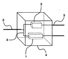
本発明において、多糖質絶縁体の原料である多糖質には、生物由来の安全かつ低コストの材料にて市販品の入手が容易であり、また多糖質水溶物の乾燥により固形化が容易かつ絶縁体として使用する際の絶縁性及び強度を保持し得るという理由から、プルラン、カルボキシメチルセルロース、デンプン、ヒアルロン酸、から選択される1の多糖質であることが好適である。また、他の多糖質としては、上述の理由に加えて生体に親和性のある新規な成形素材であるという理由から、セルロース、グリコーゲン、キチン、ヘパリン、カラギーナン、アガロース、ペクチン、キシログルカンから選択される1の多糖質を使用することが好適である。また、本発明の多糖質絶縁体の製造方法においては、電気部品及び/又は電子部品、並びに前記部品に結線する立体配線を、疎水性を有するモールド内に配置し、前記モールド内に10重量%〜70重量%の多糖質水溶物を充填した後、前記モールドを湿度10%以下の乾燥大気中に静置することにより、又は前記モールドを50℃〜90℃に加熱することにより、前記モールド内に充填された前記多糖質水溶物を乾燥固形化して成形するという多糖質絶縁体の製造方法であることが好適である。すなわち、本発明において多糖質水溶物の濃度は10重量%〜70重量%が好適であるが、10重量%より小さい場合には多糖質水溶物の乾燥固形化に非常に多大な時間がかかり過ぎて製造に不適であるいう理由から、70重量%より大きい場合では多糖質水溶物の粘度が高過ぎてモールド成形が極めて困難になるという理由から好ましくない。また、本発明において乾燥大気の湿度は10%以下が好適であるが、10%より大きい場合には多糖質水溶物の乾燥に要する時間がかかり過ぎて製造に不適であるという理由から好ましくない。さらに、本発明において加熱温度は50℃〜90℃が好適であるが、50℃より小さい場合には多糖質水溶物の加熱温度が低過ぎて乾燥に多くの時間を要し生産効率が悪くなるという理由から、90℃より大きい場合では多糖質水溶物の加熱温度が高過ぎて多糖質の表面の乾燥速度と内部の乾燥速度に大きな差が発生し、乾燥後の多糖質に歪が発生し易くなるという理由から好ましくない。また、本発明において使用するモールドは疎水性であることが好適であるが、その理由は多糖質水溶物の乾燥成形後にモールド内壁からの成形物の離形がとても容易になるからであり、モールドの材質としては例えばステンレス、鉄、チタン、シリコンなどが好適に使用され、また加熱のない乾燥大気中での乾燥の場合には例えば樹脂などが好適に使用され、さらにその形状や分割に関る構造は特には限定されない。また、前記モールド内の前記多糖質水溶物を乾燥固形化する際の前記放置の時間並びに前記加熱の時間については、絶縁体として使用に適した程度の強度があれば良く、特には限定されない。尚、本発明の多糖質絶縁体における立体配線要部を示す概略透視図を図1に示す。ここでは、電気部品1及び電子部品2が立体配線3に結線し、これらが多糖質絶縁体4内に封入され、保護されている構造のものを例示している。また、本発明において配線に使用される材質は金属であるが、電気配線として作用するものであれば例えば銅、アルミ、チタン、金、白金、ニッケルなどが好適に使用され、特に限定されない。 In the present invention, polysaccharides that are raw materials for polysaccharide insulators can be easily obtained from commercially available, safe and low-cost materials of biological origin, and can be easily solidified by drying polysaccharide aqueous solutions. It is preferable that the polysaccharide is one polysaccharide selected from pullulan, carboxymethylcellulose, starch, and hyaluronic acid because it can retain insulation and strength when used as an insulator. In addition to the above reasons, other polysaccharides are selected from cellulose, glycogen, chitin, heparin, carrageenan, agarose, pectin, and xyloglucan because they are new molding materials that have an affinity for the living body. It is preferable to use one polysaccharide. In the method for producing a polysaccharide insulator of the present invention, the electrical component and / or the electronic component and the three-dimensional wiring connected to the component are arranged in a hydrophobic mold, and 10% by weight in the mold. After filling with 70% by weight of polysaccharide aqueous solution, the mold is left in a dry atmosphere with a humidity of 10% or less, or the mold is heated to 50 ° C. to 90 ° C. It is preferable that the method for producing a polysaccharide insulator is such that the polysaccharide aqueous solution filled in is dried and solidified and molded. That is, in the present invention, the concentration of the polysaccharide water solution is preferably 10% by weight to 70% by weight, but if it is less than 10% by weight, it takes too much time to dry and solidify the polysaccharide water solution. If it is more than 70% by weight, it is not preferable because the viscosity of the polysaccharide aqueous solution is too high and molding becomes extremely difficult. In the present invention, the humidity of the dry atmosphere is preferably 10% or less. However, if it is more than 10%, it takes too much time to dry the polysaccharide water solution, which is not suitable for production. Furthermore, in the present invention, the heating temperature is preferably 50 ° C. to 90 ° C., but if it is less than 50 ° C., the heating temperature of the polysaccharide aqueous solution is too low, and it takes a long time to dry, resulting in poor production efficiency. For this reason, when the temperature is higher than 90 ° C., the heating temperature of the polysaccharide aqueous solution is too high, resulting in a large difference between the surface drying speed of the polysaccharide and the internal drying speed, and distortion of the polysaccharide after drying. It is not preferable because it becomes easy. In addition, the mold used in the present invention is preferably hydrophobic, because it is very easy to release the molded product from the inner wall of the mold after dry molding of the polysaccharide aqueous solution. For example, stainless steel, iron, titanium, silicon and the like are preferably used as the material, and in the case of drying in a dry atmosphere without heating, for example, a resin is preferably used, and further, the shape and division are related. The structure is not particularly limited. The standing time and the heating time for drying and solidifying the polysaccharide water solution in the mold are not particularly limited as long as the strength is suitable for use as an insulator. In addition, the schematic perspective view which shows the three-dimensional wiring principal part in the polysaccharide insulator of this invention is shown in FIG. Here, the electrical component 1 and the
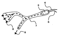
本発明において、発光ダイオード及びその照射光路を有する多糖質絶縁体には、前記電子部品を発光ダイオードとし、前記多糖質絶縁体における多糖質をプルラン又はヒアルロン酸とする発光ダイオードが封入された多糖質絶縁体であり、かつ前記発光ダイオードの照射光路を前記多糖質絶縁体内部に有するものが好適に使用される。尚、図2は本発明の発光ダイオードが封入され、かつその照射光路を有する多糖質絶縁体を示す概略模式図であるが、発光ダイオード5、及び発光ダイオードに結線された配線6、並びに発光ダイオードの照射光路を有する多糖質絶縁体7から構成されており、図2には発光ダイオードの照射光路における光の進行方向を示す矢印8が図示されている。図2より、多糖質絶縁体における照射光の出口の大小を成形制御することにより、照射光を絞ったり、拡散させたりすることが可能となる。ここで、前記の多糖質絶縁体の原料である多糖質には、生物由来の安全かつ低コストの材料にて市販品の入手が容易であり、また多糖質水溶物の乾燥により固形化が容易かつ絶縁体として使用する際の絶縁性及び強度を保持し、さらにはその成形物の透明性が高いという理由から、プルラン又はヒアルロン酸が好適に使用される。 In the present invention, the polysaccharide insulator having the light emitting diode and the irradiation optical path thereof is a polysaccharide in which the electronic component is a light emitting diode and the light emitting diode in which the polysaccharide in the polysaccharide insulator is pullulan or hyaluronic acid is enclosed. An insulator that has an irradiation light path of the light emitting diode inside the polysaccharide insulator is preferably used. FIG. 2 is a schematic diagram showing a polysaccharide insulator in which the light emitting diode of the present invention is encapsulated and having an irradiation light path. The light emitting diode 5, the wiring 6 connected to the light emitting diode, and the light emitting diode are shown. In FIG. 2, an
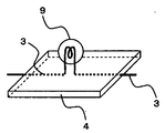
本発明において、多糖質絶縁体の応用例として、図3には本発明の電球及びその結線配線を封入した多糖質絶縁体を示す概略透視図を図示し、また図4には本発明の電球及びその結線配線を封入した多糖質絶縁体の概略断面図を図示するが、ここでは多糖質絶縁体4内部に電球9の基底部及びそれと結線した立体配線3が封入されている構造のものが示されており、本応用例では電球9の発光効果を得ることが目的である為、電球9の発光部全体が封入されるものではなく、電球9の基底部が封入されていることに留意すべきである。 In the present invention, as an application example of the polysaccharide insulator, FIG. 3 shows a schematic perspective view showing the polysaccharide insulator in which the bulb of the present invention and its wiring are enclosed, and FIG. 4 shows the bulb of the present invention. In addition, a schematic cross-sectional view of the polysaccharide insulator enclosing the wiring wiring thereof is illustrated, but here, the
以下に、本発明について実施例により具体的に説明を行うが、本発明はこれらの実施例に何ら限定されるものではない。 EXAMPLES Hereinafter, the present invention will be specifically described with reference to examples, but the present invention is not limited to these examples.
プルラン絶縁体の作製及びその絶縁性試験
電気部品であるインダクションコイル及び電子部品であるタンタルコンデンサ、並びにそれらの部品に結線する立体配線(銅線)について、疎水性を有するステンレス製モールド(内側凹部が縦長さ1cm、横長さ1cm、幅1cmの直方体形状であり、左側面及び右側面には立体配線の通し穴を各々1箇所及び2箇所設け、上面は開放され、かつ前記配線のモールド内からの取出しが可能な様に分割が施されているキャスティングモールド)内に図1で図示したように所定の空間配置を行った。次に、このモールド内に原料である60重量%のプルラン水溶物を充填した後、このモールドを60℃に加熱(約30分間)することによりモールド内に充填されたプルラン水溶物を乾燥固形化して成形を行い、図1に示した様な直方体形状のプルラン絶縁体を作製した。尚、前記モールド内からの本成形物の取り出しについては、前記モールド内で成形物が乾燥により若干縮小し、またモールド内側凹部壁は疎水性を有するので、成形物は前記モールドから自然に離形することとなり、さらに、本成形物は、絶縁体として使用に適した程度の強度を保持しており、これらのことは以下の実施例においても同様であった。また、本実施例において本成形物は直方体形状をなすが、その構成要件である3辺を縦長さ、横長さ、幅と呼ぶこととし、従って本成形物の縦長さ及び横長さとは、図1において最手前にある長方形の縦長さ及び横長さを意味し、本成形物の幅とは前記長方形及びこれと向い合う長方形との距離を表す辺を意味することとなる。それ故に、本成形物の形状はそのままモールド内側凹部の形状と同様になるため、モールド内側凹部についても前記の縦長さ、横長さ、幅の3辺を用いて大きさを表すこととし、さらに、モールド内側凹部において左側面及び右側面とは、図1における左側面(前記長方形及びこれと向い合う長方形とに連接する左側面)及び右側面(前記長方形及びこれと向い合う長方形とに連接する右側面)を表すこととし、以下の実施例においても成形物の形状及びモールド内側凹部の形状を表す3辺、さらには左側面及び右側面について上述と同様に呼ぶとすることに留意すべきである。次に、プルラン絶縁体について絶縁性試験を行うべく、上述の製作方法において独立した2本の立体配線(銅線)のみを空間配置する、とした以外は上述の製作方法と同様にして絶縁性試験用プルラン絶縁体を作製し、前記2本の電気配線間の電気抵抗を測定したところ、抵抗が2MΩ以上の絶縁体であることを確認した。Preparation of pullulan insulator and its insulation test About the induction coil that is an electrical component, the tantalum capacitor that is an electronic component, and the three-dimensional wiring (copper wire) that is connected to these components, a hydrophobic stainless steel mold (with an inner recess) It has a rectangular parallelepiped shape with a length of 1 cm, a width of 1 cm, and a width of 1 cm. The left side and the right side are each provided with one and two through holes for three-dimensional wiring, the upper surface is opened, and the wiring is formed from the mold. A predetermined space arrangement was performed as shown in FIG. 1 in a casting mold that was divided so that it could be removed. Next, after filling the mold with 60% by weight pullulan aqueous solution as a raw material, the mold is heated to 60 ° C. (about 30 minutes) to dry and solidify the pullulan aqueous solution filled in the mold. Then, a rectangular parallelepiped pullulan insulator as shown in FIG. 1 was produced. Incidentally, regarding the removal of the molded product from the mold, the molded product is slightly reduced by drying in the mold, and the concave wall inside the mold is hydrophobic, so that the molded product is naturally released from the mold. In addition, the molded product retained a strength suitable for use as an insulator, and these were the same in the following examples. Further, in this embodiment, the molded product has a rectangular parallelepiped shape, and the three sides which are constituent elements thereof are referred to as a longitudinal length, a lateral length, and a width. Therefore, the longitudinal length and the lateral length of the molded product are shown in FIG. Means the vertical length and the horizontal length of the foremost rectangle, and the width of the molded product means the side representing the distance between the rectangle and the rectangle facing the rectangle. Therefore, since the shape of the molded product is the same as the shape of the recess inside the mold as it is, the mold inner recess also represents the size using the three sides of the vertical length, the horizontal length, and the width. The left side surface and the right side surface in the concave portion on the inner side of the mold are the left side surface in FIG. It should be noted that, in the following examples, the three sides representing the shape of the molded product and the shape of the concave portion inside the mold, and the left side surface and the right side surface are also referred to as described above. . Next, in order to conduct an insulation test on the pullulan insulator, insulation is performed in the same manner as in the above manufacturing method except that only two three-dimensional wirings (copper wires) that are independent in the above manufacturing method are spatially arranged. When a pullulan insulator for test was prepared and the electric resistance between the two electric wires was measured, it was confirmed that the resistor was an insulator having a resistance of 2 MΩ or more.
ヒアルロン酸絶縁体の作製及びその絶縁性試験
実施例1において、原料に50重量%のヒアルロン酸水溶物を使用し、原料充填後のモールド内容物の乾燥固形化を湿度5%の乾燥大気中に静置(約60分間)することによる、とした以外は実施例1と同様にして、図1に示した様な直方体形状のヒアルロン酸絶縁体を作製した。次に、ヒアルロン酸絶縁体について絶縁性試験を行うべく、上述の製作方法において独立した2本の立体配線(銅線)のみを空間配置する、とした以外は上述の製作方法と同様にして絶縁性試験用ヒアルロン酸絶縁体を作製し、前記2本の電気配線間の電気抵抗を測定したところ、抵抗が2MΩ以上の絶縁体であることを確認した。Preparation of Hyaluronic Acid Insulator and its Insulation Test In Example 1, 50% by weight of hyaluronic acid aqueous solution was used as a raw material, and the solidification of the mold contents after filling the raw material was performed in a dry atmosphere of 5% humidity A rectangular parallelepiped hyaluronic acid insulator as shown in FIG. 1 was produced in the same manner as in Example 1 except that it was left standing (about 60 minutes). Next, in order to conduct an insulation test on the hyaluronic acid insulator, insulation was performed in the same manner as in the above manufacturing method except that only two independent three-dimensional wirings (copper wires) were spatially arranged in the above manufacturing method. When a hyaluronic acid insulator for property test was prepared and the electrical resistance between the two electrical wirings was measured, it was confirmed that the resistance was 2 MΩ or more.
カルボキシメチルセルロース絶縁体の作製及びその絶縁性試験
実施例1において、原料に40重量%のカルボキシメチルセルロース水溶物を使用し、原料充填後のモールド内容物の乾燥固形化を70℃に加熱(約30分間)することによる、とした以外は実施例1と同様にして、図1に示した様な直方体形状のカルボキシメチルセルロース絶縁体を作製した。次に、カルボキシメチルセルロース絶縁体について絶縁性試験を行うべく、上述の製作方法において独立した2本の立体配線(銅線)のみを空間配置する、とした以外は上述の製作方法と同様にして絶縁性試験用カルボキシメチルセルロース絶縁体を作製し、前記2本の電気配線間の電気抵抗を測定したところ、抵抗が2MΩ以上の絶縁体であることを確認した。Preparation of carboxymethylcellulose insulator and insulation test thereof In Example 1, 40% by weight of carboxymethylcellulose aqueous solution was used as a raw material, and the solidification of the mold contents after filling the raw material was heated to 70 ° C. (about 30 minutes) A rectangular parallelepiped carboxymethylcellulose insulator as shown in FIG. 1 was produced in the same manner as in Example 1 except that the above was changed. Next, in order to conduct an insulation test on the carboxymethyl cellulose insulator, insulation was performed in the same manner as in the above manufacturing method except that only two three-dimensional wirings (copper wires) that were independent in the above manufacturing method were spatially arranged. A carboxymethylcellulose insulator for property test was prepared, and the electrical resistance between the two electrical wirings was measured. As a result, it was confirmed that the resistance was 2 MΩ or more.
発光ダイオード及びその照射光路を有したプルラン絶縁体の作製、並びにその光照射試験
始めに、照射光路のベースとなるプルラン絶縁体を得るべく、50重量%のプルラン水溶物を60℃(約40分間)で加熱乾燥して、2種の丸棒形状(直径約1cm及び長さ約10cm、直径約2cm及び長さ約5cm)のプルラン絶縁体を作製した。次に、前者及び後者の丸棒を水に浸漬して任意の屈曲形状に変形できる状態にした上で、前者の丸棒の長さ方向の中間部位に後者の丸棒を付着させて一体とし、さらに前者の丸棒の末端部に対して、電子部品である発光ダイオード(直径0.5cmタイプ)並びにそれに結線する2本の立体配線(銅線)を挿入した後に成形物全体を自然乾燥させ、図2に示したようなプルラン絶縁体を作成した。尚、本プルラン絶縁体は、絶縁体として使用に適した程度の強度を保持していた。次に、本プルラン絶縁体について、前記の配線に電気を通して光照射試験を行ったところ、発光ダイオードより照射された光はプルラン絶縁体内の照射光路を通り、図2に示した様に照射光の出口より光照射されることを確認した。その際、前者の丸棒の出口面における照射光は、後者の丸棒の照射光の出口面における照射光と比べて、照射光の面積が小さく、照射光が絞られていることを確認した。Preparation of light-emitting diode and pullulan insulator having its irradiation light path, and light irradiation test First, in order to obtain a pullulan insulator serving as a base of the irradiation light path, 50 wt. ) To produce pullulan insulators of two types of round bars (diameter about 1 cm and length about 10 cm, diameter about 2 cm and length about 5 cm). Next, the former and the latter round bar are immersed in water so that they can be deformed into an arbitrary bent shape, and then the latter round bar is attached to the intermediate part in the length direction of the former round bar and integrated. Furthermore, after inserting a light emitting diode (0.5 cm diameter type) which is an electronic component and two three-dimensional wirings (copper wires) connected to the end of the former round bar, the whole molded product is naturally dried. A pullulan insulator as shown in FIG. 2 was prepared. In addition, this pullulan insulator kept the intensity | strength suitable for use as an insulator. Next, a light irradiation test was conducted on the pullulan insulator through electricity to the wiring. As a result, the light irradiated from the light-emitting diode passed through the irradiation light path in the pullulan insulator, and as shown in FIG. It was confirmed that light was irradiated from the exit. At that time, it was confirmed that the irradiation light on the exit surface of the former round bar was smaller in area than the irradiation light on the exit surface of the latter round bar, and the irradiation light was narrowed down. .
電球及びその結線配線を有したプルラン絶縁体の作製、並びにその照光試験
電気部品である電球(豆電球タイプ)、並びにそれらの部品に結線する立体配線(銅線)について、疎水性を有するステンレス製モールド(内側凹部が縦長さ0.5cm、横長さ1cm、幅3cmの直方体形状であり、左側面及び右側面には立体配線の通し穴を各々1箇所設け、上面は開放され、かつ前記配線のモールド内からの取出しが可能な様に分割が施されているキャスティングモールド)内に図3及び図4で図示したように所定の空間配置を行った。その後、このモールド内に原料である40重量%のプルラン水溶物を充填した後、このモールドを70℃に加熱(約30分間)することによりモールド内に充填されたプルラン水溶物を乾燥固形化して成形を行い、図3及び図4に示した様な電球及びその結線配線を有した直方体形状のプルラン絶縁体を作製した。次に、本プルラン絶縁体について、前記の配線に電気を通して照光試験を行ったところ、電球が明瞭に照光することを確認した。Production of pullulan insulators with light bulbs and their connection wiring, and their illumination test Electric bulbs (bean bulb type), and three-dimensional wiring (copper wires) connected to these components are made of hydrophobic stainless steel Mold (inner recess has a rectangular parallelepiped shape with a vertical length of 0.5 cm, a horizontal length of 1 cm, and a width of 3 cm, one through hole for three-dimensional wiring is provided on each of the left and right sides, the top surface is open, and the wiring A predetermined space arrangement was performed as shown in FIGS. 3 and 4 in a casting mold (divided so that it can be taken out from the mold). After that, after filling the mold with 40% by weight pullulan aqueous solution as a raw material, the mold is heated to 70 ° C. (about 30 minutes) to dry and solidify the pullulan aqueous solution filled in the mold. Molding was performed to produce a rectangular parallelepiped pullulan insulator having a light bulb and its wiring as shown in FIGS. Next, when an illumination test was conducted on the pullulan insulator by passing electricity through the wiring, it was confirmed that the bulb was clearly illuminated.
本発明の多糖質絶縁体及びその製造方法は、前述の通り様々な特徴的効果を有するが、これらの効果を活かして絶縁体技術分野、絶縁体を用いた発光ダイオードの応用技術分野等において実用的に利用され得る。また、本発明の多糖質絶縁体及びその製造方法は量産実施が可能なものであり、産業上利用できるものである。 The polysaccharide insulator of the present invention and the method for producing the same have various characteristic effects as described above. Utilizing these effects, the polysaccharide insulator is practically used in the insulator technical field, the application technical field of the light emitting diode using the insulator, and the like. Can be used. Moreover, the polysaccharide insulator of the present invention and the production method thereof can be mass-produced and can be used industrially.
1 電気部品
2 電子部品
3 立体配線
4 多糖質絶縁体
5 発光ダイオード
6 発光ダイオードに結線された配線
7 発光ダイオードの照射光路を有する多糖質絶縁体
8 照射光路における光の進行方向を示す矢印
9 電球DESCRIPTION OF SYMBOLS 1
Claims (4)
Priority Applications (1)
| Application Number | Priority Date | Filing Date | Title |
|---|---|---|---|
| JP2008335997A JP2010141277A (en) | 2008-12-10 | 2008-12-10 | Polysaccharide insulator and method of manufacturing the same |
Applications Claiming Priority (1)
| Application Number | Priority Date | Filing Date | Title |
|---|---|---|---|
| JP2008335997A JP2010141277A (en) | 2008-12-10 | 2008-12-10 | Polysaccharide insulator and method of manufacturing the same |
Publications (1)
| Publication Number | Publication Date |
|---|---|
| JP2010141277A true JP2010141277A (en) | 2010-06-24 |
Family
ID=42351112
Family Applications (1)
| Application Number | Title | Priority Date | Filing Date |
|---|---|---|---|
| JP2008335997A Pending JP2010141277A (en) | 2008-12-10 | 2008-12-10 | Polysaccharide insulator and method of manufacturing the same |
Country Status (1)
| Country | Link |
|---|---|
| JP (1) | JP2010141277A (en) |
-
2008
- 2008-12-10 JP JP2008335997A patent/JP2010141277A/en active Pending
Similar Documents
| Publication | Publication Date | Title |
|---|---|---|
| US20150177171A1 (en) | Gas sensor package | |
| CN102709454A (en) | Surface-roughened double-layer adhesive structure LED light source and manufacturing method thereof | |
| CN101853914A (en) | High power LED white light source structure | |
| JP2010141277A (en) | Polysaccharide insulator and method of manufacturing the same | |
| RU2016116029A (en) | MASS FOR MOVING PLUGS, MOVING PLUG AND METHOD FOR PRODUCING MOVING PLUGS | |
| CN203982928U (en) | Glass insulator sintering mold | |
| Cui et al. | Floatable Liquid Metal Porous Hydrogel with Hydrogen Production for Flexible Sensor and Energy Harvesting | |
| CN202710202U (en) | Sensor with strong waterproofness | |
| TW200834998A (en) | Light emitting diode package with odds of lead frame removed from its surface and method for fabricating the same | |
| CN103694471B (en) | Method for preparing poly(o-phenylenediamine) nanomicelle by utilizing aqueous phase method | |
| JP2010141278A (en) | Polysaccharide wiring board and method of manufacturing the same | |
| CN207674379U (en) | PCB substrate LED module | |
| CN201623047U (en) | Resin circuit board chip is mounted with heat sink package structure | |
| CN203055979U (en) | Novel LED (Light-Emitting Diode) packaging structure | |
| CN208835038U (en) | A kind of multistage photoelectric device bracket | |
| CN204209357U (en) | A kind of suspended fuse type fuse | |
| CN105632948A (en) | Corrosive liquid and dissection process for internal structure dissection of surface mount device | |
| CN205488206U (en) | Encapsulation LED | |
| CN110277936B (en) | A flexible and repairable triboelectric nanogenerator and its application | |
| CN202797068U (en) | Patched type laser packaging structure | |
| CN203179945U (en) | LED packaging structure | |
| CN202817016U (en) | Novel TOP LED metal support | |
| CN202285243U (en) | Photovoltaic assembly junction box and cable positioning device thereof | |
| CN203850290U (en) | Plastic-sealed lead frame suitable for high-temperature electrical appliances | |
| CN201623061U (en) | Base Island Embedded Chip Front Mount Locking Hole Heat Slug Package Structure |
Legal Events
| Date | Code | Title | Description |
|---|---|---|---|
| A621 | Written request for application examination |
Effective date: 20111206 Free format text: JAPANESE INTERMEDIATE CODE: A621 |
|
| A072 | Dismissal of procedure |
Effective date: 20130514 Free format text: JAPANESE INTERMEDIATE CODE: A073 |