JP2010141231A - Method for manufacturing semiconductor device, and semiconductor device - Google Patents
Method for manufacturing semiconductor device, and semiconductor device Download PDFInfo
- Publication number
- JP2010141231A JP2010141231A JP2008318100A JP2008318100A JP2010141231A JP 2010141231 A JP2010141231 A JP 2010141231A JP 2008318100 A JP2008318100 A JP 2008318100A JP 2008318100 A JP2008318100 A JP 2008318100A JP 2010141231 A JP2010141231 A JP 2010141231A
- Authority
- JP
- Japan
- Prior art keywords
- groove
- semiconductor device
- film
- substrate
- manufacturing
- Prior art date
- Legal status (The legal status is an assumption and is not a legal conclusion. Google has not performed a legal analysis and makes no representation as to the accuracy of the status listed.)
- Granted
Links
Images


Classifications
-
- H—ELECTRICITY
- H01—ELECTRIC ELEMENTS
- H01L—SEMICONDUCTOR DEVICES NOT COVERED BY CLASS H10
- H01L21/00—Processes or apparatus adapted for the manufacture or treatment of semiconductor or solid state devices or of parts thereof
- H01L21/70—Manufacture or treatment of devices consisting of a plurality of solid state components formed in or on a common substrate or of parts thereof; Manufacture of integrated circuit devices or of parts thereof
- H01L21/71—Manufacture of specific parts of devices defined in group H01L21/70
- H01L21/76—Making of isolation regions between components
- H01L21/762—Dielectric regions, e.g. EPIC dielectric isolation, LOCOS; Trench refilling techniques, SOI technology, use of channel stoppers
- H01L21/76224—Dielectric regions, e.g. EPIC dielectric isolation, LOCOS; Trench refilling techniques, SOI technology, use of channel stoppers using trench refilling with dielectric materials
- H01L21/76232—Dielectric regions, e.g. EPIC dielectric isolation, LOCOS; Trench refilling techniques, SOI technology, use of channel stoppers using trench refilling with dielectric materials of trenches having a shape other than rectangular or V-shape, e.g. rounded corners, oblique or rounded trench walls
Abstract
Description
本発明は、半導体装置の製造方法及び半導体装置に関する。 The present invention relates to a semiconductor device manufacturing method and a semiconductor device.
異なる電位の素子領域同士を電気的に絶縁(素子分離)する方法として、基板に、側壁を絶縁層で覆った溝を形成し、この溝にポリシリコン膜等を埋め込む方法がある。溝にポリシリコン膜等を埋め込むときには、溝内及び基板上にポリシリコン膜を形成し、基板上のポリシリコン膜を、ドライエッチング等を用いて除去する。 As a method of electrically insulating (isolating elements) element regions having different potentials, there is a method in which a groove having a sidewall covered with an insulating layer is formed in a substrate and a polysilicon film or the like is embedded in the groove. When embedding a polysilicon film or the like in the groove, a polysilicon film is formed in the groove and on the substrate, and the polysilicon film on the substrate is removed by dry etching or the like.
溝に膜を埋め込む場合、溝の開口幅の1/2以上の膜を形成する必要がある。一方、溝が交差する交差部分では、溝の開口幅が他の部分よりも広く(例えば直交する場合は約1.4倍)なる。 このため、溝の交差部分では、膜を形成した後に中央部に深い窪みが形成されやすい。この窪みを残しておくと、基板上に絶縁膜を形成するときに絶縁膜が窪みを埋めきれず、その結果ボイドが形成されることがある。 In the case of embedding a film in the groove, it is necessary to form a film having a width equal to or greater than ½ of the groove opening width. On the other hand, at the intersection where the grooves intersect, the opening width of the groove is wider than that of the other parts (for example, about 1.4 times in the case of being orthogonal). For this reason, at the intersection of the grooves, a deep depression is likely to be formed in the center after the film is formed. If this recess is left, the insulating film cannot fill the recess when forming the insulating film on the substrate, and as a result, a void may be formed.
上記したボイドの発生を抑制する方法として、例えば特許文献1に記載の方法がある。この方法は、基板に溝を形成するときに、溝の交差部分に、この交差部分より狭い面積の島パターンを形成するものである。
しかし、半導体装置の微細化が進んだ場合、特許文献1に記載の方法では、島パターンの面積が小さくなる。この場合、島パターンを形成するためのレジストパターンにおいて、底面積に対する高さの比が大きくなり、レジストパターンが不安定になり、倒れやすくなってしまう。このため、半導体装置の歩留まりが低下してしまう。 However, when the semiconductor device is further miniaturized, the method described in Patent Document 1 reduces the area of the island pattern. In this case, in the resist pattern for forming the island pattern, the ratio of the height to the bottom area becomes large, and the resist pattern becomes unstable and easily falls down. For this reason, the yield of a semiconductor device will fall.
本発明によれば、基板に第1の溝及び前記第1の溝と交差する第2の溝を形成する工程と、
前記基板に対して成膜処理を行うことにより、前記第1の溝内及び前記第2の溝内に膜を埋め込む工程と、
前記基板上に位置する前記膜を除去する工程と、
を備え、
前記第1の溝及び前記第2の溝を形成する工程において、前記第1の溝と前記第2の溝の交差部分に、平面視において前記交差部分の角の一つから前記交差部分の中央に向けて延伸する凸部を形成する半導体装置の製造方法が提供される。
According to the present invention, forming a first groove and a second groove intersecting the first groove on the substrate;
Embedding a film in the first groove and the second groove by performing a film forming process on the substrate;
Removing the film located on the substrate;
With
In the step of forming the first groove and the second groove, the intersection of the first groove and the second groove is formed at one of the corners of the intersection in plan view from the center of the intersection. There is provided a method of manufacturing a semiconductor device that forms a convex portion extending toward the surface.
この半導体装置の製造方法によれば、平面視において凸部が、第1の溝と第2の溝の交差部分の角の一つから交差部分の中央に向けて延伸している。このため、交差部分において溝の開口幅を狭くすることができる。従って、第1の溝及び第2の溝に膜を埋め込むときに、交差部分の中央部に深い窪みが形成されることを抑制できる。また、凸部を形成するためのレジストパターンは孤立しないため、レジストパターンが不安定になって半導体装置の歩留まりが低下することを抑制できる。 According to this method for manufacturing a semiconductor device, the convex portion extends from one corner of the intersection of the first groove and the second groove toward the center of the intersection in plan view. For this reason, the opening width of the groove can be narrowed at the intersection. Therefore, when a film is embedded in the first groove and the second groove, it is possible to suppress the formation of a deep depression at the center of the intersecting portion. In addition, since the resist pattern for forming the convex portion is not isolated, it can be suppressed that the resist pattern becomes unstable and the yield of the semiconductor device is reduced.
本発明によれば、基板と、
前記基板に形成された第1の溝と、
前記基板に形成され、前記第1の溝と交差する第2の溝と、
前記第1の溝と前記第2の溝の交差部分に形成され、平面視において前記交差部分の角の一つから前記交差部分の中央に向けて延伸する凸部と
前記第1の溝内及び前記第2の溝内に埋め込まれた膜と、
を備える半導体装置が提供される。
According to the present invention, a substrate;
A first groove formed in the substrate;
A second groove formed in the substrate and intersecting the first groove;
A convex portion formed at an intersection of the first groove and the second groove and extending from one corner of the intersection in the plan view toward the center of the intersection; and in the first groove and A film embedded in the second groove;
A semiconductor device is provided.
本発明によれば、溝の交差部分の中央部に窪みが形成されることを抑制でき、かつ半導体装置の歩留まりが低下することを抑制できる。 According to the present invention, it is possible to suppress the formation of a depression at the center of the intersecting portion of the grooves, and it is possible to suppress a decrease in the yield of the semiconductor device.
以下、本発明の実施の形態について、図面を用いて説明する。尚、すべての図面において、同様な構成要素には同様の符号を付し、適宜説明を省略する。 Hereinafter, embodiments of the present invention will be described with reference to the drawings. In all the drawings, the same reference numerals are given to the same components, and the description will be omitted as appropriate.
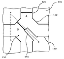
図1〜図5は、実施形態に係る半導体装置の製造方法を説明するための図である。図1及び図5は平面図であり、図2、図3、及び図4は図1及び図5のc−a−b断面図である。この半導体装置の製造方法は、基板100に第1の溝110及び第1の溝110と交差する第2の溝120を形成する工程と、基板100に対して成膜処理を行うことにより、第1の溝110内及び第2の溝120内に膜200を埋め込む工程と、基板100上に位置する膜200を除去する工程とを備える。そして第1の溝110及び第2の溝120を形成する工程において、第1の溝110と第2の溝120の交差部分130に、平面視において交差部分130の角の一つから交差部分130の中央に向けて延伸する凸部140を形成する。以下、詳細に説明する。
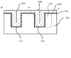
1 to 5 are diagrams for explaining a method of manufacturing a semiconductor device according to the embodiment. 1 and 5 are plan views, and FIGS. 2, 3, and 4 are cross-sectional views taken along the line c-a-b in FIGS. In this method for manufacturing a semiconductor device, a
まず図1及び図2に示すように、シリコン基板などの半導体基板100上にレジスト膜(図示せず)を形成し、このレジスト膜を露光及び現像する。これにより、半導体基板100上にはレジストパターンが形成される。次いで、このレジストパターンをマスクとして半導体基板100をエッチングする。これにより、半導体基板100には第1の溝110、第2の溝120、及び凸部140が形成される。
First, as shown in FIGS. 1 and 2, a resist film (not shown) is formed on a
この工程において、凸部140を形成するためのレジストパターンは孤立せず、他のレジストパターンに繋がっている。このため、レジストパターンが不安定になって半導体装置の歩留まりが低下することを抑制できる。
In this step, the resist pattern for forming the
本図に示す例では、平面視において、第1の溝110及び第2の溝120は直交しており、かつ凸部140は、第1の溝110の延伸方向に対して45°の角度で延伸している。ただし第1の溝110及び第2の溝120が直交していない場合、凸部140が第1の溝110の延伸方向に対して成す角度は45°とは異なる角度になる。
In the example shown in this drawing, the
また凸部140は略長方形である。そして交差部分130の4つの角102は、それぞれ凸部140の側面のうち対向する面と平行に面取りされている。
Moreover, the
本実施形態において、4つの角102それぞれから凸部140までの距離Bは全て等しくなっている。また第1の溝110の幅及び第2の溝120の幅は互いに等しいが、角102から凸部140までの距離Bは、第1の溝110及び第2の溝120の幅A以下、好ましくは幅Aと等しくなっている。
In the present embodiment, the distances B from the four
なお、半導体基板100をエッチングして第1の溝110、第2の溝120、及び凸部140を形成する工程において、レジストパターンではなく窒化シリコン膜などのハードマスクを用いても良い。この場合、上記したレジストパターンは、半導体基板100上に形成されたハードマスクに開口パターンを形成するときに用いられる。
Note that a hard mask such as a silicon nitride film may be used instead of the resist pattern in the step of forming the
次いで図3に示すように、半導体基板100の表面、並びに第1の溝110及び第2の溝120の底面及び側面に、絶縁層104を形成する。絶縁層104は、例えば熱酸化膜であるが、プラズマCVD法により形成されてもよい。半導体基板100がシリコン基板である場合、絶縁層104は酸化シリコン膜である。
Next, as illustrated in FIG. 3, the
次いで絶縁層104上に膜200を例えばプラズマCVD法を用いて成膜する。半導体基板100がシリコン基板である場合、膜200は例えばポリシリコン膜である。上記したように、交差部分130には凸部140が延伸しており、交差部分130における開口の幅は小さくなる。従って、第1の溝110及び第2の溝120に膜200を埋め込むときに、交差部分130の中央部に形成される窪み204が深くなることを抑制できる。この窪み204の深さは、例えば第1の溝110の中央部に形成される窪み202と同程度の深さである。
Next, the
その後、図4及び図5に示すように、半導体基板100上に形成された膜200を、例えばエッチバック法により除去する。上記したように、交差部分130の中央部に形成される窪み204が深くなることを抑制できる。このため、エッチバック後に深い窪み204が残ることを抑制できる。なお、膜200がポリシリコン膜である場合、膜200をグランド配線として用いることができる。
Thereafter, as shown in FIGS. 4 and 5, the
次に、本実施形態の効果について説明する。上記したように、凸部140は交差部分130の角の一つから交差部分130の中央に向けて延伸している。このため、凸部140を形成するためのレジストパターンは孤立せず、他のレジストパターンに繋がっている。従って、レジストパターンが不安定になって半導体装置の歩留まりが低下することを抑制できる。
Next, the effect of this embodiment will be described. As described above, the
また、交差部分130には凸部140が延伸しているため、交差部分130における開口の幅は小さくなる。従って、第1の溝110及び第2の溝120に膜200を埋め込むときに、交差部分130の中央部に形成される窪み204が深くなることを抑制できる。
Moreover, since the
特に凸部140の平面形状が長方形であり、交差部分130の4つの角102は、それぞれ凸部140の側面のうち対向する面と平行に面取りされている場合、交差部分130における膜200の埋め込み不良が生じることを抑制でき、かつ交差部分130内で開口の幅が部分的に広くなることを抑制できる(例えば開口幅Bを第1の溝110の開口幅A以下にすることができる)ため、上記した効果が顕著になる。
In particular, when the planar shape of the
なお、凸部140の形状は、本実施形態に示した例に限定されない。また、交差部分130の角102は面取りされていなくても良い。また膜200は酸化シリコン膜であっても良い。
In addition, the shape of the
以上、図面を参照して本発明の実施形態について述べたが、これらは本発明の例示であり、上記以外の様々な構成を採用することもできる。 As mentioned above, although embodiment of this invention was described with reference to drawings, these are the illustrations of this invention, Various structures other than the above are also employable.
100 基板
102 角
104 絶縁層
110 第1の溝
120 第2の溝
130 交差部分
140 凸部
200 膜
202 窪み
204 窪み
100
Claims (10)
前記基板に対して成膜処理を行うことにより、前記第1の溝内及び前記第2の溝内に膜を埋め込む工程と、
前記基板上に位置する前記膜を除去する工程と、
を備え、
前記第1の溝及び前記第2の溝を形成する工程において、前記第1の溝と前記第2の溝の交差部分に、平面視において前記交差部分の角の一つから前記交差部分の中央に向けて延伸する凸部を形成する半導体装置の製造方法。 Forming a first groove on the substrate and a second groove intersecting the first groove;
Embedding a film in the first groove and the second groove by performing a film forming process on the substrate;
Removing the film located on the substrate;
With
In the step of forming the first groove and the second groove, the intersection of the first groove and the second groove is formed at one of the corners of the intersection in plan view from the center of the intersection. Manufacturing method of semiconductor device which forms convex part extended toward
前記第1の溝及び前記第2の溝を形成する工程において、
前記第1の溝及び前記第2の溝を直交させ、
前記凸部を前記第1の溝の延伸方向に対して45°の角度で延伸させる半導体装置の製造方法。 In the manufacturing method of the semiconductor device according to claim 1,
In the step of forming the first groove and the second groove,
Making the first groove and the second groove orthogonal,
The manufacturing method of the semiconductor device which extends the said convex part at an angle of 45 degrees with respect to the extending direction of the said 1st groove | channel.
前記第1の溝及び前記第2の溝を形成する工程において、
前記凸部を平面視において略長方形にして、
前記交差部分の4つの角を、前記凸部の側面のうち対向する面と平行に面取りする半導体装置の製造方法。 In the manufacturing method of the semiconductor device according to claim 1 or 2,
In the step of forming the first groove and the second groove,
The convex portion is substantially rectangular in plan view,
A method of manufacturing a semiconductor device, wherein the four corners of the intersecting portion are chamfered in parallel with opposing surfaces of the side surfaces of the convex portion.
前記第1の溝及び前記第2の溝を形成する工程において、
前記第1の溝及び前記第2の溝の幅を等しくして、
前記交差部分の4つの角それぞれを、前記凸部のうち前記角に対向する側面までの距離が前記第1の溝の幅と等しくなるように面取りする半導体装置の製造方法。 In the manufacturing method of the semiconductor device according to claim 3,
In the step of forming the first groove and the second groove,
The widths of the first groove and the second groove are made equal,
A method of manufacturing a semiconductor device, wherein each of the four corners of the intersecting portion is chamfered so that a distance to a side surface of the convex portion that faces the corner is equal to a width of the first groove.
前記基板はシリコン基板であり、
前記膜はポリシリコン膜であり、
前記第1の溝及び前記第2の溝を形成した後、前記膜を埋め込む工程の間に、前記第1の溝及び前記第2の溝に酸化シリコン膜を形成する工程を有する半導体装置の製造方法。 In the manufacturing method of the semiconductor device in any one of Claims 1-4,
The substrate is a silicon substrate;
The film is a polysilicon film;
Manufacturing of a semiconductor device including a step of forming a silicon oxide film in the first groove and the second groove after the step of embedding the film after forming the first groove and the second groove. Method.
前記基板に形成された第1の溝と、
前記基板に形成され、前記第1の溝と交差する第2の溝と、
前記第1の溝と前記第2の溝の交差部分に形成され、平面視において前記交差部分の角の一つから前記交差部分の中央に向けて延伸する凸部と
前記第1の溝内及び前記第2の溝内に埋め込まれた膜と、
を備える半導体装置。 A substrate,
A first groove formed in the substrate;
A second groove formed in the substrate and intersecting the first groove;
A convex portion formed at an intersection of the first groove and the second groove and extending from one corner of the intersection in the plan view toward the center of the intersection; and in the first groove and A film embedded in the second groove;
A semiconductor device comprising:
前記第1の溝は前記第2の溝に直交しており、
平面視において、前記凸部は前記第1の溝の延伸方向に対して45°の角度で延伸する半導体装置。 The semiconductor device according to claim 6.
The first groove is orthogonal to the second groove;
In plan view, the convex portion extends at an angle of 45 ° with respect to the extending direction of the first groove.
前記凸部は平面視において略長方形であり、
前記交差部分の4つの角は、前記凸部のうち前記角に対向する側面と平行に面取りされている半導体装置。 The semiconductor device according to claim 6 or 7,
The convex portion is substantially rectangular in plan view,
The four corners of the intersecting portion are chamfered parallel to the side surface of the convex portion that faces the corner.
前記第1の溝及び前記第2の溝の幅は等しく、
前記交差部分の4つの角それぞれは、前記凸部のうち前記角に対向する側面までの距離が前記第1の溝の幅と等しくなるように面取りされている半導体装置。 The semiconductor device according to claim 8,
The widths of the first groove and the second groove are equal,
Each of the four corners of the intersecting portion is chamfered so that the distance to the side surface of the convex portion that faces the corner is equal to the width of the first groove.
前記基板はシリコン基板であり、
前記膜はポリシリコン膜であり、
前記第1の溝及び前記第2の溝の側壁及び底面は酸化シリコン膜を有する半導体装置。 In the semiconductor device according to any one of claims 6 to 9,
The substrate is a silicon substrate;
The film is a polysilicon film;
A semiconductor device in which side walls and bottom surfaces of the first groove and the second groove have silicon oxide films.
Priority Applications (3)
| Application Number | Priority Date | Filing Date | Title |
|---|---|---|---|
| JP2008318100A JP5527964B2 (en) | 2008-12-15 | 2008-12-15 | Semiconductor device manufacturing method and semiconductor device |
| US12/591,932 US8377794B2 (en) | 2008-12-15 | 2009-12-04 | Method of manufacturing semiconductor device, and semiconductor device |
| CN2009102590341A CN101794728B (en) | 2008-12-15 | 2009-12-09 | Method of manufacturing semiconductor device and semiconductor device thereof |
Applications Claiming Priority (1)
| Application Number | Priority Date | Filing Date | Title |
|---|---|---|---|
| JP2008318100A JP5527964B2 (en) | 2008-12-15 | 2008-12-15 | Semiconductor device manufacturing method and semiconductor device |
Publications (2)
| Publication Number | Publication Date |
|---|---|
| JP2010141231A true JP2010141231A (en) | 2010-06-24 |
| JP5527964B2 JP5527964B2 (en) | 2014-06-25 |
Family
ID=42239502
Family Applications (1)
| Application Number | Title | Priority Date | Filing Date |
|---|---|---|---|
| JP2008318100A Expired - Fee Related JP5527964B2 (en) | 2008-12-15 | 2008-12-15 | Semiconductor device manufacturing method and semiconductor device |
Country Status (3)
| Country | Link |
|---|---|
| US (1) | US8377794B2 (en) |
| JP (1) | JP5527964B2 (en) |
| CN (1) | CN101794728B (en) |
Families Citing this family (2)
| Publication number | Priority date | Publication date | Assignee | Title |
|---|---|---|---|---|
| US9391001B2 (en) | 2013-08-26 | 2016-07-12 | Micron Technology, Inc. | Semiconductor constructions |
| KR20210092916A (en) * | 2020-01-17 | 2021-07-27 | 삼성전자주식회사 | Wiring structures and vertical memory devices including the same |
Citations (6)
| Publication number | Priority date | Publication date | Assignee | Title |
|---|---|---|---|---|
| JPH04264752A (en) * | 1991-02-20 | 1992-09-21 | Fujitsu Ltd | Photomask and manufacture of semiconductor device |
| JPH04274344A (en) * | 1991-03-01 | 1992-09-30 | Matsushita Electron Corp | Manufacture of semiconductor device |
| JPH10308443A (en) * | 1997-05-02 | 1998-11-17 | Nec Corp | Semiconductor integrated circuit device |
| DE102005059034A1 (en) * | 2005-12-10 | 2007-06-14 | X-Fab Semiconductor Foundries Ag | Isolation grave structure |
| JP2008130826A (en) * | 2006-11-21 | 2008-06-05 | Rohm Co Ltd | Semiconductor device, and method of fabricating semiconductor device |
| DE102008029235B3 (en) * | 2008-06-19 | 2009-10-08 | X-Fab Semiconductor Foundries Ag | Intersections of isolation trenches of SOI technology |
Family Cites Families (6)
| Publication number | Priority date | Publication date | Assignee | Title |
|---|---|---|---|---|
| US5094973A (en) * | 1987-11-23 | 1992-03-10 | Texas Instrument Incorporated | Trench pillar for wafer processing |
| JPH04127148A (en) | 1990-09-19 | 1992-04-28 | Hitachi Ltd | Mask and production of semiconductor device formed by using this mask |
| KR100249025B1 (en) * | 1998-03-06 | 2000-03-15 | 김영환 | Semiconductor element isolating method |
| JP4127148B2 (en) | 2003-07-14 | 2008-07-30 | 富士ゼロックス株式会社 | Image reading device |
| KR100525111B1 (en) * | 2004-04-19 | 2005-11-01 | 주식회사 하이닉스반도체 | Semiconductor device |
| DE102005059035B4 (en) * | 2005-12-10 | 2007-11-08 | X-Fab Semiconductor Foundries Ag | Isolation trench structures for high voltages |
-
2008
- 2008-12-15 JP JP2008318100A patent/JP5527964B2/en not_active Expired - Fee Related
-
2009
- 2009-12-04 US US12/591,932 patent/US8377794B2/en not_active Expired - Fee Related
- 2009-12-09 CN CN2009102590341A patent/CN101794728B/en not_active Expired - Fee Related
Patent Citations (9)
| Publication number | Priority date | Publication date | Assignee | Title |
|---|---|---|---|---|
| JPH04264752A (en) * | 1991-02-20 | 1992-09-21 | Fujitsu Ltd | Photomask and manufacture of semiconductor device |
| JPH04274344A (en) * | 1991-03-01 | 1992-09-30 | Matsushita Electron Corp | Manufacture of semiconductor device |
| JPH10308443A (en) * | 1997-05-02 | 1998-11-17 | Nec Corp | Semiconductor integrated circuit device |
| DE102005059034A1 (en) * | 2005-12-10 | 2007-06-14 | X-Fab Semiconductor Foundries Ag | Isolation grave structure |
| WO2007065953A1 (en) * | 2005-12-10 | 2007-06-14 | X-Fab Semiconductor Foundries Ag | Isolation trench intersection structure with reduced gap width |
| JP2009518839A (en) * | 2005-12-10 | 2009-05-07 | エックス−ファブ・セミコンダクター・ファウンダリーズ・アーゲー | Insulating trench intersection structure with reduced slit width |
| JP2008130826A (en) * | 2006-11-21 | 2008-06-05 | Rohm Co Ltd | Semiconductor device, and method of fabricating semiconductor device |
| DE102008029235B3 (en) * | 2008-06-19 | 2009-10-08 | X-Fab Semiconductor Foundries Ag | Intersections of isolation trenches of SOI technology |
| WO2009153356A1 (en) * | 2008-06-19 | 2009-12-23 | X-Fab Semiconductor Foundries Ag | Semiconductor component with isolation trench intersections |
Also Published As
| Publication number | Publication date |
|---|---|
| US20100148299A1 (en) | 2010-06-17 |
| CN101794728B (en) | 2013-05-08 |
| JP5527964B2 (en) | 2014-06-25 |
| US8377794B2 (en) | 2013-02-19 |
| CN101794728A (en) | 2010-08-04 |
Similar Documents
| Publication | Publication Date | Title |
|---|---|---|
| KR20090085642A (en) | Methods of etching a pattern layer to form staggered heights therein and intermediate semiconductor device structures | |
| KR100816733B1 (en) | Method for fabricating recess gate in semiconductor device | |
| CN108206156A (en) | Semiconductor devices and the method for manufacturing it | |
| JP4610323B2 (en) | Manufacturing method of semiconductor device having recess channel region | |
| US20150279727A1 (en) | Method of manufacturing semiconductor device | |
| US10043675B2 (en) | Semiconductor device and method for fabricating the same | |
| US7595252B2 (en) | Method of manufacturing a semiconductor memory device | |
| JP5527964B2 (en) | Semiconductor device manufacturing method and semiconductor device | |
| JP5064687B2 (en) | Manufacturing method of semiconductor device | |
| JP2006135067A (en) | Semiconductor device and manufacturing method thereof | |
| JP2007201409A (en) | Semiconductor device and its forming method | |
| US7485543B2 (en) | Method for manufacturing semiconductor device with overlay vernier | |
| KR100720258B1 (en) | Method for forming semiconductor device | |
| JP4987244B2 (en) | Manufacturing method of semiconductor device | |
| JP2006128613A (en) | Manufacture of semiconductor element | |
| JP2009177069A (en) | Method of manufacturing semiconductor device | |
| KR20090025746A (en) | Semiconductor device and method for manufacturing the same | |
| KR20070073053A (en) | Semiconductor device and method for forming the same | |
| CN108807267B (en) | Semiconductor device and method for manufacturing the same | |
| JP2008130826A (en) | Semiconductor device, and method of fabricating semiconductor device | |
| KR100802221B1 (en) | Method for forming semiconductor device | |
| KR20070002594A (en) | Method for forming overlay vernier of semiconductor device | |
| KR100887064B1 (en) | Overlay vernier and method for forming the same | |
| TWI532096B (en) | Process of forming slit in substrate | |
| KR20110075935A (en) | Semiconductor device and method for forming using the same |
Legal Events
| Date | Code | Title | Description |
|---|---|---|---|
| A621 | Written request for application examination |
Free format text: JAPANESE INTERMEDIATE CODE: A621 Effective date: 20111017 |
|
| A977 | Report on retrieval |
Free format text: JAPANESE INTERMEDIATE CODE: A971007 Effective date: 20130612 |
|
| A131 | Notification of reasons for refusal |
Free format text: JAPANESE INTERMEDIATE CODE: A131 Effective date: 20130618 |
|
| A521 | Written amendment |
Free format text: JAPANESE INTERMEDIATE CODE: A523 Effective date: 20130807 |
|
| TRDD | Decision of grant or rejection written | ||
| A01 | Written decision to grant a patent or to grant a registration (utility model) |
Free format text: JAPANESE INTERMEDIATE CODE: A01 Effective date: 20140401 |
|
| A61 | First payment of annual fees (during grant procedure) |
Free format text: JAPANESE INTERMEDIATE CODE: A61 Effective date: 20140415 |
|
| R150 | Certificate of patent or registration of utility model |
Ref document number: 5527964 Country of ref document: JP Free format text: JAPANESE INTERMEDIATE CODE: R150 |
|
| S531 | Written request for registration of change of domicile |
Free format text: JAPANESE INTERMEDIATE CODE: R313531 |
|
| R350 | Written notification of registration of transfer |
Free format text: JAPANESE INTERMEDIATE CODE: R350 |
|
| LAPS | Cancellation because of no payment of annual fees |