JP2010141204A - Wiring board and method of manufacturing the same - Google Patents
Wiring board and method of manufacturing the same Download PDFInfo
- Publication number
- JP2010141204A JP2010141204A JP2008317410A JP2008317410A JP2010141204A JP 2010141204 A JP2010141204 A JP 2010141204A JP 2008317410 A JP2008317410 A JP 2008317410A JP 2008317410 A JP2008317410 A JP 2008317410A JP 2010141204 A JP2010141204 A JP 2010141204A
- Authority
- JP
- Japan
- Prior art keywords
- layer
- pad
- forming
- cavity
- insulating layer
- Prior art date
- Legal status (The legal status is an assumption and is not a legal conclusion. Google has not performed a legal analysis and makes no representation as to the accuracy of the status listed.)
- Granted
Links
Images

Classifications
-
- H—ELECTRICITY
- H10—SEMICONDUCTOR DEVICES; ELECTRIC SOLID-STATE DEVICES NOT OTHERWISE PROVIDED FOR
- H10W—GENERIC PACKAGES, INTERCONNECTIONS, CONNECTORS OR OTHER CONSTRUCTIONAL DETAILS OF DEVICES COVERED BY CLASS H10
- H10W70/00—Package substrates; Interposers; Redistribution layers [RDL]
- H10W70/60—Insulating or insulated package substrates; Interposers; Redistribution layers
- H10W70/67—Insulating or insulated package substrates; Interposers; Redistribution layers characterised by their insulating layers or insulating parts
- H10W70/68—Shapes or dispositions thereof
-
- H—ELECTRICITY
- H05—ELECTRIC TECHNIQUES NOT OTHERWISE PROVIDED FOR
- H05K—PRINTED CIRCUITS; CASINGS OR CONSTRUCTIONAL DETAILS OF ELECTRIC APPARATUS; MANUFACTURE OF ASSEMBLAGES OF ELECTRICAL COMPONENTS
- H05K3/00—Apparatus or processes for manufacturing printed circuits
- H05K3/46—Manufacturing multilayer circuits
- H05K3/4697—Manufacturing multilayer circuits having cavities, e.g. for mounting components
-
- H—ELECTRICITY
- H10—SEMICONDUCTOR DEVICES; ELECTRIC SOLID-STATE DEVICES NOT OTHERWISE PROVIDED FOR
- H10W—GENERIC PACKAGES, INTERCONNECTIONS, CONNECTORS OR OTHER CONSTRUCTIONAL DETAILS OF DEVICES COVERED BY CLASS H10
- H10W70/00—Package substrates; Interposers; Redistribution layers [RDL]
- H10W70/60—Insulating or insulated package substrates; Interposers; Redistribution layers
- H10W70/67—Insulating or insulated package substrates; Interposers; Redistribution layers characterised by their insulating layers or insulating parts
- H10W70/68—Shapes or dispositions thereof
- H10W70/685—Shapes or dispositions thereof comprising multiple insulating layers
-
- H—ELECTRICITY
- H10—SEMICONDUCTOR DEVICES; ELECTRIC SOLID-STATE DEVICES NOT OTHERWISE PROVIDED FOR
- H10W—GENERIC PACKAGES, INTERCONNECTIONS, CONNECTORS OR OTHER CONSTRUCTIONAL DETAILS OF DEVICES COVERED BY CLASS H10
- H10W90/00—Package configurations
-
- H—ELECTRICITY
- H05—ELECTRIC TECHNIQUES NOT OTHERWISE PROVIDED FOR
- H05K—PRINTED CIRCUITS; CASINGS OR CONSTRUCTIONAL DETAILS OF ELECTRIC APPARATUS; MANUFACTURE OF ASSEMBLAGES OF ELECTRICAL COMPONENTS
- H05K1/00—Printed circuits
- H05K1/18—Printed circuits structurally associated with non-printed electric components
- H05K1/182—Printed circuits structurally associated with non-printed electric components associated with components mounted in printed circuit boards [PCB], e.g. insert-mounted components [IMC]
- H05K1/183—Printed circuits structurally associated with non-printed electric components associated with components mounted in printed circuit boards [PCB], e.g. insert-mounted components [IMC] associated with components mounted in and supported by recessed areas of the PCBs
-
- H—ELECTRICITY
- H05—ELECTRIC TECHNIQUES NOT OTHERWISE PROVIDED FOR
- H05K—PRINTED CIRCUITS; CASINGS OR CONSTRUCTIONAL DETAILS OF ELECTRIC APPARATUS; MANUFACTURE OF ASSEMBLAGES OF ELECTRICAL COMPONENTS
- H05K2201/00—Indexing scheme relating to printed circuits covered by H05K1/00
- H05K2201/09—Shape and layout
- H05K2201/09209—Shape and layout details of conductors
- H05K2201/09372—Pads and lands
- H05K2201/09472—Recessed pad for surface mounting; Recessed electrode of component
-
- H—ELECTRICITY
- H05—ELECTRIC TECHNIQUES NOT OTHERWISE PROVIDED FOR
- H05K—PRINTED CIRCUITS; CASINGS OR CONSTRUCTIONAL DETAILS OF ELECTRIC APPARATUS; MANUFACTURE OF ASSEMBLAGES OF ELECTRICAL COMPONENTS
- H05K2201/00—Indexing scheme relating to printed circuits covered by H05K1/00
- H05K2201/09—Shape and layout
- H05K2201/09209—Shape and layout details of conductors
- H05K2201/09372—Pads and lands
- H05K2201/09481—Via in pad; Pad over filled via
-
- H—ELECTRICITY
- H05—ELECTRIC TECHNIQUES NOT OTHERWISE PROVIDED FOR
- H05K—PRINTED CIRCUITS; CASINGS OR CONSTRUCTIONAL DETAILS OF ELECTRIC APPARATUS; MANUFACTURE OF ASSEMBLAGES OF ELECTRICAL COMPONENTS
- H05K2201/00—Indexing scheme relating to printed circuits covered by H05K1/00
- H05K2201/10—Details of components or other objects attached to or integrated in a printed circuit board
- H05K2201/10613—Details of electrical connections of non-printed components, e.g. special leads
- H05K2201/10621—Components characterised by their electrical contacts
- H05K2201/10674—Flip chip
-
- H—ELECTRICITY
- H05—ELECTRIC TECHNIQUES NOT OTHERWISE PROVIDED FOR
- H05K—PRINTED CIRCUITS; CASINGS OR CONSTRUCTIONAL DETAILS OF ELECTRIC APPARATUS; MANUFACTURE OF ASSEMBLAGES OF ELECTRICAL COMPONENTS
- H05K2203/00—Indexing scheme relating to apparatus or processes for manufacturing printed circuits covered by H05K3/00
- H05K2203/03—Metal processing
- H05K2203/0369—Etching selective parts of a metal substrate through part of its thickness, e.g. using etch resist
-
- H—ELECTRICITY
- H05—ELECTRIC TECHNIQUES NOT OTHERWISE PROVIDED FOR
- H05K—PRINTED CIRCUITS; CASINGS OR CONSTRUCTIONAL DETAILS OF ELECTRIC APPARATUS; MANUFACTURE OF ASSEMBLAGES OF ELECTRICAL COMPONENTS
- H05K2203/00—Indexing scheme relating to apparatus or processes for manufacturing printed circuits covered by H05K3/00
- H05K2203/03—Metal processing
- H05K2203/0376—Etching temporary metallic carrier substrate
-
- H—ELECTRICITY
- H05—ELECTRIC TECHNIQUES NOT OTHERWISE PROVIDED FOR
- H05K—PRINTED CIRCUITS; CASINGS OR CONSTRUCTIONAL DETAILS OF ELECTRIC APPARATUS; MANUFACTURE OF ASSEMBLAGES OF ELECTRICAL COMPONENTS
- H05K3/00—Apparatus or processes for manufacturing printed circuits
- H05K3/10—Apparatus or processes for manufacturing printed circuits in which conductive material is applied to the insulating support in such a manner as to form the desired conductive pattern
- H05K3/20—Apparatus or processes for manufacturing printed circuits in which conductive material is applied to the insulating support in such a manner as to form the desired conductive pattern by affixing prefabricated conductor pattern
- H05K3/205—Apparatus or processes for manufacturing printed circuits in which conductive material is applied to the insulating support in such a manner as to form the desired conductive pattern by affixing prefabricated conductor pattern using a pattern electroplated or electroformed on a metallic carrier
-
- H—ELECTRICITY
- H05—ELECTRIC TECHNIQUES NOT OTHERWISE PROVIDED FOR
- H05K—PRINTED CIRCUITS; CASINGS OR CONSTRUCTIONAL DETAILS OF ELECTRIC APPARATUS; MANUFACTURE OF ASSEMBLAGES OF ELECTRICAL COMPONENTS
- H05K3/00—Apparatus or processes for manufacturing printed circuits
- H05K3/46—Manufacturing multilayer circuits
- H05K3/4644—Manufacturing multilayer circuits by building the multilayer layer by layer, i.e. build-up multilayer circuits
- H05K3/4682—Manufacture of core-less build-up multilayer circuits on a temporary carrier or on a metal foil
-
- H—ELECTRICITY
- H10—SEMICONDUCTOR DEVICES; ELECTRIC SOLID-STATE DEVICES NOT OTHERWISE PROVIDED FOR
- H10W—GENERIC PACKAGES, INTERCONNECTIONS, CONNECTORS OR OTHER CONSTRUCTIONAL DETAILS OF DEVICES COVERED BY CLASS H10
- H10W70/00—Package substrates; Interposers; Redistribution layers [RDL]
- H10W70/60—Insulating or insulated package substrates; Interposers; Redistribution layers
- H10W70/62—Insulating or insulated package substrates; Interposers; Redistribution layers characterised by their interconnections
- H10W70/63—Vias, e.g. via plugs
- H10W70/635—Through-vias
-
- H—ELECTRICITY
- H10—SEMICONDUCTOR DEVICES; ELECTRIC SOLID-STATE DEVICES NOT OTHERWISE PROVIDED FOR
- H10W—GENERIC PACKAGES, INTERCONNECTIONS, CONNECTORS OR OTHER CONSTRUCTIONAL DETAILS OF DEVICES COVERED BY CLASS H10
- H10W72/00—Interconnections or connectors in packages
-
- H—ELECTRICITY
- H10—SEMICONDUCTOR DEVICES; ELECTRIC SOLID-STATE DEVICES NOT OTHERWISE PROVIDED FOR
- H10W—GENERIC PACKAGES, INTERCONNECTIONS, CONNECTORS OR OTHER CONSTRUCTIONAL DETAILS OF DEVICES COVERED BY CLASS H10
- H10W74/00—Encapsulations, e.g. protective coatings
- H10W74/10—Encapsulations, e.g. protective coatings characterised by their shape or disposition
- H10W74/15—Encapsulations, e.g. protective coatings characterised by their shape or disposition on active surfaces of flip-chip devices, e.g. underfills
-
- H—ELECTRICITY
- H10—SEMICONDUCTOR DEVICES; ELECTRIC SOLID-STATE DEVICES NOT OTHERWISE PROVIDED FOR
- H10W—GENERIC PACKAGES, INTERCONNECTIONS, CONNECTORS OR OTHER CONSTRUCTIONAL DETAILS OF DEVICES COVERED BY CLASS H10
- H10W90/00—Package configurations
- H10W90/701—Package configurations characterised by the relative positions of pads or connectors relative to package parts
- H10W90/721—Package configurations characterised by the relative positions of pads or connectors relative to package parts of bump connectors
- H10W90/722—Package configurations characterised by the relative positions of pads or connectors relative to package parts of bump connectors between stacked chips
-
- H—ELECTRICITY
- H10—SEMICONDUCTOR DEVICES; ELECTRIC SOLID-STATE DEVICES NOT OTHERWISE PROVIDED FOR
- H10W—GENERIC PACKAGES, INTERCONNECTIONS, CONNECTORS OR OTHER CONSTRUCTIONAL DETAILS OF DEVICES COVERED BY CLASS H10
- H10W90/00—Package configurations
- H10W90/701—Package configurations characterised by the relative positions of pads or connectors relative to package parts
- H10W90/721—Package configurations characterised by the relative positions of pads or connectors relative to package parts of bump connectors
- H10W90/724—Package configurations characterised by the relative positions of pads or connectors relative to package parts of bump connectors between a chip and a stacked insulating package substrate, interposer or RDL
-
- H—ELECTRICITY
- H10—SEMICONDUCTOR DEVICES; ELECTRIC SOLID-STATE DEVICES NOT OTHERWISE PROVIDED FOR
- H10W—GENERIC PACKAGES, INTERCONNECTIONS, CONNECTORS OR OTHER CONSTRUCTIONAL DETAILS OF DEVICES COVERED BY CLASS H10
- H10W90/00—Package configurations
- H10W90/701—Package configurations characterised by the relative positions of pads or connectors relative to package parts
- H10W90/731—Package configurations characterised by the relative positions of pads or connectors relative to package parts of die-attach connectors
- H10W90/734—Package configurations characterised by the relative positions of pads or connectors relative to package parts of die-attach connectors between a chip and a stacked insulating package substrate, interposer or RDL
-
- Y—GENERAL TAGGING OF NEW TECHNOLOGICAL DEVELOPMENTS; GENERAL TAGGING OF CROSS-SECTIONAL TECHNOLOGIES SPANNING OVER SEVERAL SECTIONS OF THE IPC; TECHNICAL SUBJECTS COVERED BY FORMER USPC CROSS-REFERENCE ART COLLECTIONS [XRACs] AND DIGESTS
- Y10—TECHNICAL SUBJECTS COVERED BY FORMER USPC
- Y10T—TECHNICAL SUBJECTS COVERED BY FORMER US CLASSIFICATION
- Y10T156/00—Adhesive bonding and miscellaneous chemical manufacture
- Y10T156/10—Methods of surface bonding and/or assembly therefor
Landscapes
- Engineering & Computer Science (AREA)
- Manufacturing & Machinery (AREA)
- Microelectronics & Electronic Packaging (AREA)
- Production Of Multi-Layered Print Wiring Board (AREA)
Abstract
【課題】低コストでPOP(パッケージ・オン・パッケージ)接続を容易に行えるようにし、その接続信頼性の向上を図ると共に、小型・薄型化に寄与すること。
【解決手段】配線基板(パッケージ)10は、その一方の面側の最外層の絶縁層12の、チップ搭載エリアに対応する箇所にキャビティCVが形成され、このキャビティCV内の絶縁層12の表面に露出するパッドP1と、キャビティCVの周囲の絶縁層12の表面に露出するパッドP2とを備えている。そして、このパッケージ10のキャビティCV内のパッドP1にチップ31がフリップチップ接続され、キャビティCVの周囲のパッドP2に他のパッケージ40が接続されて、POP構造の半導体装置30を構成している。
【選択図】図5A POP (Package-on-Package) connection can be easily performed at a low cost, the connection reliability is improved, and the size and thickness are reduced.
A wiring substrate (package) 10 has a cavity CV formed at a position corresponding to a chip mounting area of an outermost insulating layer 12 on one surface side, and the surface of the insulating layer 12 in the cavity CV. And a pad P2 exposed on the surface of the insulating layer 12 around the cavity CV. Then, the chip 31 is flip-chip connected to the pad P1 in the cavity CV of the package 10, and another package 40 is connected to the pad P2 around the cavity CV to constitute the semiconductor device 30 having the POP structure.
[Selection] Figure 5
Description
本発明は、配線基板及びその製造方法に関し、より詳細には、半導体素子(チップ)等の搭載用もしくは外部接続用の端子(パッド)が最外層の絶縁層から露出した構造を有した配線基板及びその製造方法に関する。 The present invention relates to a wiring board and a manufacturing method thereof, and more specifically, a wiring board having a structure in which a terminal (pad) for mounting a semiconductor element (chip) or the like or external connection is exposed from an outermost insulating layer. And a manufacturing method thereof.
かかる配線基板は、半導体チップ等を搭載するパッケージとしての機能を果たすという点で、以下の記述では便宜上、「半導体パッケージ」ともいう。 Such a wiring board is also referred to as a “semiconductor package” in the following description for convenience in that it functions as a package on which a semiconductor chip or the like is mounted.
配線基板(半導体パッケージ)に半導体チップ等の電子部品を搭載して半導体装置を構成するにあたり、その小型・薄型化及び高性能(高機能)化の流れの中で、実装面積削減のため、半導体チップ等を搭載したパッケージ同士を上下方向(高さ方向)に積層するPOP(パッケージ・オン・パッケージ)接合の要求がある。 In order to reduce the mounting area in the trend of miniaturization, thinning, and high performance (high function) in configuring semiconductor devices by mounting electronic components such as semiconductor chips on a wiring board (semiconductor package) There is a need for POP (package-on-package) bonding in which packages with chips or the like are stacked in the vertical direction (height direction).
かかるPOP接合を実現する方法の一つとして、上下のパッケージ間にインターポーザを介在させて接続する方法がある。これは、下側パッケージ(配線基板)に半導体チップをフリップチップ接続するとともに、この下側パッケージ上で当該チップの周辺領域に形成された端子(パッド)に、上側パッケージ(配線基板)の実装面側の対応する領域に形成された端子(パッド)を、当該チップの厚さ(その電極端子を含む)よりも厚いインターポーザの両面にそれぞれ形成された外部端子を介して接合した構造である。 As one method for realizing such POP bonding, there is a method in which an interposer is interposed between upper and lower packages. This is because the semiconductor chip is flip-chip connected to the lower package (wiring board), and the upper package (wiring board) mounting surface is connected to the terminals (pads) formed in the peripheral area of the chip on the lower package. In this structure, terminals (pads) formed in corresponding regions on the side are joined via external terminals respectively formed on both surfaces of the interposer thicker than the thickness of the chip (including the electrode terminals).
この接続方法では、インターポーザを製造するためのプロセスも別途必要となる。その典型的なプロセスは、コア材を用意→その所要箇所にスルーホールを形成→そのスルーホールに導体を充填後、両面にレジスト層を形成→導体に接続させて所要のパターンに配線層を形成→レジスト層を除去→配線層の外部端子形成部を露出させて絶縁層(ソルダレジスト層)を形成→外部端子形成部に所要のめっき(ニッケル/金めっきなど)を施す工程等を含む。 This connection method requires a separate process for manufacturing the interposer. The typical process is to prepare a core material → form a through hole at the required location → fill the through hole with a conductor and then form a resist layer on both sides → connect to the conductor and form a wiring layer in the required pattern → Removing resist layer → Exposing insulating layer (solder resist layer) by exposing external terminal forming portion of wiring layer → Containing required plating (nickel / gold plating or the like) to external terminal forming portion.
また、上記のPOP接合を実現する他の方法として、はんだを用いて上下各パッケージの端子(パッド)同士を接続する方法がある。これは、下側パッケージ(配線基板)に半導体チップをフリップチップ接続するとともに、この下側パッケージ上で当該チップの周辺領域に形成された端子(パッド)に、上側パッケージ(配線基板)の実装面側の対応する領域に形成された端子(パッド)を、はんだバンプを介して接合した構造である。 As another method for realizing the above POP bonding, there is a method of connecting terminals (pads) of the upper and lower packages using solder. This is because the semiconductor chip is flip-chip connected to the lower package (wiring board), and the upper package (wiring board) mounting surface is connected to the terminals (pads) formed in the peripheral area of the chip on the lower package. In this structure, terminals (pads) formed in corresponding regions on the side are joined via solder bumps.
かかるPOP接合に関連する技術として、特許文献1に記載されたものがある。この文献には、ソルダボールによりトップ基板(配線基板)と電気的に繋がるパッケージ・オン・パッケージのボトム基板(配線基板)が開示されており、このボトム基板は、コア基板と、ソルダボールの位置に応じてコア基板の表面に形成されるパッドと、コア基板に積層される絶縁層と、上記パッドが露出されるように絶縁層の一部を除去して形成される貫通ホールと、この貫通ホールに充填されてソルダボールと電気的に繋がる金属層とを備えている。
上述したように従来の技術では、POP接合(接続)を実現するために、インターポーザによる接続や、はんだによる接続などが行われている。しかしながら、インターポーザによる接続の場合、そのインターポーザを製造するためのプロセス(相当の製造工程)を別途必要とし、またそのための材料も必要となるため、製造コストが増大するといった問題があった。 As described above, in the conventional technology, in order to realize POP bonding (connection), connection by an interposer, connection by solder, or the like is performed. However, in the case of connection by an interposer, there is a problem in that the manufacturing cost increases because a process (equivalent manufacturing process) for manufacturing the interposer is separately required and a material for the process is also required.
一方、はんだによる接続の場合、上下パッケージ間に搭載チップが介在している分、パッケージ間の間隔が大きいため、パッケージ間を接続するはんだ(バンプ)の使用量も多くなり、リフローの際にそのバンプが分断されたり(はんだの泣き別れ)、隣接するバンプ間で橋絡(ブリッジ)が生じたりするなどの不都合があった。その結果、上下パッケージ間の接続信頼性が低下するといった問題があった。 On the other hand, in the case of connection by solder, the amount of solder (bump) used to connect between packages increases because the mounting chip is interposed between the upper and lower packages. There have been inconveniences such as bumps being divided (solder crying) and bridging between adjacent bumps. As a result, there is a problem that connection reliability between the upper and lower packages is lowered.
また、いずれの方法による接続の場合も、上下パッケージ間に搭載チップが介在している分、POP構造全体として見た場合に、そのチップの厚さにも依るが、必ずしも所望の小型・薄型化を達成することができないといった課題もあった。 In addition, in any connection method, since the mounted chip is interposed between the upper and lower packages, the overall size of the POP structure depends on the thickness of the chip. There was also a problem that could not be achieved.
本発明は、かかる従来技術における課題に鑑み創作されたもので、低コストでPOP接続を容易に行えるようにし、その接続信頼性の向上を図ると共に、小型・薄型化に寄与することができる配線基板及びその製造方法を提供することを目的とする。 The present invention has been created in view of the problems in the prior art, and enables easy POP connection at a low cost, improves the connection reliability, and contributes to a reduction in size and thickness. An object of the present invention is to provide a substrate and a manufacturing method thereof.
上述した従来技術の課題を解決するため、本発明の一形態によれば、支持基材上に、形成すべきキャビティの位置に対応する部分のみが残存するようパターン形成された第1のレジスト層を形成する工程と、前記第1のレジスト層をマスクにして前記支持基材を所要量だけ除去し、段差部を有した支持基材を形成する工程と、前記第1のレジスト層を除去後、前記支持基材の段差部が形成されている側の面に、該段差部の上の部分及び下の部分に対応する箇所にそれぞれ第1の開口部及び第2の開口部を有するようパターン形成された第2のレジスト層を形成する工程と、前記第2のレジスト層の第1、第2の各開口部から露出している前記支持基材上に、それぞれ第1のパッド及び第2のパッドを形成する工程と、前記第2のレジスト層を除去後、前記支持基材上に、前記第1、第2の各パッドを覆う絶縁層を形成する工程と、前記絶縁層の上面から前記各パッドの一部を露出させる開口を形成する工程と、前記絶縁層上に、前記各パッドにそれぞれ接続されるビアを含む配線層を形成する工程と、以降、所要の層数となるまで絶縁層と配線層を交互に積層した後、前記支持基材を除去する工程とを含むことを特徴とする配線基板の製造方法が提供される。 In order to solve the above-described problems of the prior art, according to one aspect of the present invention, a first resist layer patterned so that only a portion corresponding to the position of a cavity to be formed remains on a support substrate. Forming a supporting substrate having a stepped portion by removing the supporting substrate by a required amount using the first resist layer as a mask, and after removing the first resist layer A pattern in which the first opening and the second opening are respectively provided on the surface of the support base on which the step portion is formed at locations corresponding to the upper portion and the lower portion of the step portion. A step of forming the formed second resist layer, and a first pad and a second pad on the supporting base material exposed from the first and second openings of the second resist layer, respectively. Forming the pad, and the second resist layer After leaving, a step of forming an insulating layer covering each of the first and second pads on the supporting base, and a step of forming an opening exposing a part of each pad from the upper surface of the insulating layer; A step of forming a wiring layer including vias connected to the respective pads on the insulating layer, and thereafter, alternately laminating the insulating layer and the wiring layer until the required number of layers is obtained, And a step of removing the material. A method for manufacturing a wiring board is provided.
この形態に係る配線基板の製造方法によれば、最終的に得られる配線基板において最外層の絶縁層(例えば、樹脂層)の電子部品搭載エリアに対応する箇所にキャビティが形成され、このキャビティ内の絶縁層の表面に第1のパッドが露出し、かつ、キャビティの周囲の絶縁層の表面に第2のパッドが露出している。つまり、第1のパッドが露出する絶縁層の表面の高さが、第2のパッドが露出する絶縁層の表面よりも低くなるように形成されている。従って、キャビティの周囲に配置された第2のパッドをPOP接合(接続)用の端子として利用することで、POP接続を容易に行うことができる。 According to the method for manufacturing a wiring board according to this embodiment, a cavity is formed at a location corresponding to the electronic component mounting area of the outermost insulating layer (for example, resin layer) in the finally obtained wiring board. The first pad is exposed on the surface of the insulating layer, and the second pad is exposed on the surface of the insulating layer around the cavity. That is, the surface of the insulating layer where the first pad is exposed is formed to be lower than the surface of the insulating layer where the second pad is exposed. Therefore, the POP connection can be easily performed by using the second pad arranged around the cavity as a terminal for POP bonding (connection).
すなわち、本配線基板に搭載する電子部品(半導体チップなど)をキャビティ内に収容できるので、その周囲の第2のパッドに接続される他のパッケージとの間隔を相対的に狭くすることができる。このため、従来技術で使用されていたようなインターポーザを介在させなくても、その狭められた間隔に応じた少量のはんだ(はんだバンプなど)を介して上下パッケージ間の接続(POP接続)を容易に行うことが可能となる。つまり、POP接続を行うに際し、インターポーザが不要となることで、コストの低減化を図ることができる。 That is, since an electronic component (semiconductor chip or the like) to be mounted on the wiring board can be accommodated in the cavity, the distance from other packages connected to the surrounding second pads can be relatively narrowed. For this reason, it is easy to connect the upper and lower packages (POP connection) via a small amount of solder (solder bumps, etc.) corresponding to the narrowed interval without interposing the interposer used in the prior art. Can be performed. That is, the cost can be reduced by eliminating the need for an interposer when performing POP connection.
また、POP接続を行う際、上下パッケージ間を接続するはんだ(バンプ)の使用量が少なくて済むので、従来技術に見られたような不都合(はんだの泣き別れやブリッジ等)を解消することができる。これは、接続信頼性の向上に寄与する。 In addition, when performing POP connection, the amount of solder (bump) used to connect the upper and lower packages can be reduced, which eliminates inconveniences (eg, solder crying and bridging) as seen in the prior art. . This contributes to improved connection reliability.
さらに、搭載する電子部品をキャビティ内に収容できるので、本配線基板の高さを相対的に低くすることができ、小型・薄型化に寄与する。その結果、POP構造を実現するにあたり、所望の小型・薄型化を達成することが可能となる。 Furthermore, since the electronic component to be mounted can be accommodated in the cavity, the height of the present wiring board can be relatively lowered, contributing to a reduction in size and thickness. As a result, in realizing the POP structure, it is possible to achieve a desired small size and thickness.
また、本発明の他の形態によれば、支持基材上に、形成すべきキャビティの位置に対応する箇所に開口部を有するようパターン形成された第1のレジスト層を形成する工程と、前記第1のレジスト層の開口部から露出している前記支持基材上に、犠牲導体層を所要の厚さに形成して、段差部を有した支持基材を形成する工程と、前記第1のレジスト層を除去後、前記支持基材の段差部が形成されている側の面に、該段差部の上の部分の犠牲導体層上及び該段差部の下の部分に対応する箇所にそれぞれ第1の開口部及び第2の開口部を有するようパターン形成された第2のレジスト層を形成する工程と、前記第2のレジスト層の第1、第2の各開口部から露出している前記犠牲導体層及び前記支持基材上に、それぞれ第1のパッド及び第2のパッドを形成する工程と、前記第2のレジスト層を除去後、前記犠牲導体層及び前記支持基材上に、前記第1、第2の各パッドを露出させて絶縁層を形成する工程と、前記絶縁層の上面から前記各パッドの一部を露出させる開口を形成する工程と、前記絶縁層上に、前記各パッドにそれぞれ接続されるビアを含む配線層を形成する工程と、以降、所要の層数となるまで絶縁層と配線層を交互に積層した後、前記支持基材及び前記犠牲導体層を除去する工程とを含むことを特徴とする配線基板の製造方法が提供される。 According to another aspect of the present invention, a step of forming a first resist layer patterned so as to have an opening at a location corresponding to the position of the cavity to be formed on the support substrate; Forming a sacrificial conductor layer in a required thickness on the support substrate exposed from the opening of the first resist layer to form a support substrate having a stepped portion; After removing the resist layer, on the surface of the support base on which the stepped portion is formed, on the sacrificial conductor layer on the portion above the stepped portion and on the portion corresponding to the portion below the stepped portion, respectively. Forming a second resist layer patterned to have a first opening and a second opening, and being exposed from the first and second openings of the second resist layer; A first pad and a second pad are formed on the sacrificial conductor layer and the support substrate, respectively. Forming an insulating layer; and, after removing the second resist layer, exposing the first and second pads on the sacrificial conductor layer and the supporting base, and forming an insulating layer; A step of forming an opening exposing a part of each pad from the upper surface of the insulating layer, a step of forming a wiring layer including vias respectively connected to the pads on the insulating layer, and thereafter required And a step of removing the supporting base material and the sacrificial conductor layer after alternately laminating insulating layers and wiring layers until the number of layers is reached.
この形態に係る配線基板の製造方法においても、上記の形態に係る配線基板の製造方法と同様に、最終的に得られる配線基板は同じ構成を有しているので、同様の作用効果を奏することができる。 Also in the method for manufacturing a wiring board according to this embodiment, as the wiring board manufacturing method according to the above-described embodiment, the finally obtained wiring board has the same configuration, and thus has the same effects. Can do.
また、本発明の更に他の形態によれば、一方の面側の最外層の絶縁層の、電子部品の搭載エリアに対応する箇所にキャビティが形成され、前記キャビティ内の前記絶縁層の表面に露出する第1のパッドと、前記キャビティの周囲の前記絶縁層の表面に露出する第2のパッドとを備えたことを特徴とする配線基板が提供される。 According to still another embodiment of the present invention, a cavity is formed at a location corresponding to the mounting area of the electronic component in the outermost insulating layer on one side, and the surface of the insulating layer in the cavity is formed. There is provided a wiring board comprising: an exposed first pad; and a second pad exposed on a surface of the insulating layer around the cavity.
本発明に係る配線基板及びその製造方法の他の構成上の特徴及びそれに基づく有利な利点等については、以下に記述する発明の実施の形態を参照しながら説明する。 Other structural features of the wiring board and the manufacturing method thereof according to the present invention and advantageous advantages based thereon will be described with reference to the embodiments of the invention described below.
以下、本発明の好適な実施の形態について、添付の図面を参照しながら説明する。 DESCRIPTION OF EXEMPLARY EMBODIMENTS Hereinafter, preferred embodiments of the invention will be described with reference to the accompanying drawings.
(第1の実施形態…図1〜図6参照)
図1は本発明の第1の実施形態に係る配線基板(半導体パッケージ)の構成を断面図の形態で示したものである。
(First embodiment: see FIGS. 1 to 6)
FIG. 1 shows a configuration of a wiring board (semiconductor package) according to a first embodiment of the present invention in the form of a sectional view.
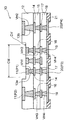
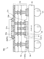
本実施形態に係る配線基板(半導体パッケージ)10は、図示のように、複数の配線層11,14,17,20が絶縁層(具体的には、樹脂層)12,15,18を介在させて積層され、各々の絶縁層12,15,18に形成されたビアホールVH1及びVH2,VH3,VH4にそれぞれ充填された導体(ビア13a及び13b、16,19)を介して層間接続された構造を有している。つまり、本パッケージ10は、一般的なビルドアップ法を用いて作製される配線基板(支持基材としてのコア基板の両面/片面に所要数のビルドアップ層を順次形成して積み上げていくもの)とは違い、支持基材を含まない「コアレス基板」の形態を有している。
In the wiring substrate (semiconductor package) 10 according to the present embodiment, as shown in the figure, a plurality of
このコアレス基板の一方の面側(図示の例では上側)の最外層の樹脂層12には、本発明を特徴付ける凹部(キャビティ)CVが形成されている。このキャビティCVには、本パッケージ10に搭載される半導体素子等の電子部品(チップ)が収容される。従って、このキャビティCVは、図示のように樹脂層12上のチップ搭載エリアCMに対応する箇所に、このエリアよりも若干大きいサイズで、所要の深さに形成されている。
A concave portion (cavity) CV characterizing the present invention is formed in the
また、このキャビティCVは、チップを収容する役割の他に、後述するように本パッケージ10にチップを搭載してその間隙にアンダーフィル樹脂を充填したときに、その間隙から周囲に流れ出す樹脂を堰き止めるための「ダム」としての役割も果たす。
In addition to the role of accommodating the chip, the cavity CV dams the resin that flows out from the gap when the chip is mounted on the
キャビティCVが形成されている側の面には、2種類のパッドP1,P2(配線層11の所要の箇所に画定された部分)が露出しており、各パッドP1,P2は、図示のようにその表面が樹脂層12の表面と同一面となるように形成されている。ただし、パッドP1はキャビティCV内のチップ搭載エリアCMに配置され、パッドP2はキャビティCVの周囲の領域に配置されているので、パッドP1の表面は、図示のようにキャビティCVの深さに相当する分だけ、パッドP2の表面の位置から下側(基板内側)に後退した位置にある。
Two types of pads P1 and P2 (parts defined at required portions of the wiring layer 11) are exposed on the surface on which the cavity CV is formed, and each pad P1 and P2 is as shown in the figure. The surface of the
一方、パッドP1,P2が形成されている側と反対側の面(図示の例では下側)には、保護膜として機能するソルダレジスト層(絶縁層)21が、最外層の配線層(図示の例では配線層20)の所要の箇所に画定されたパッドP3,P4の部分を除いてその表面を覆うように形成されている。このソルダレジスト層21から露出する各パッドP3,P4のうち、パッドP3は、ビア19、配線層17、ビア16、配線層14及びビア13aを介してチップ搭載エリアCM内のパッドP1に接続されている。また、パッドP4は、ビア19、配線層17、ビア16、配線層14及びビア13bを介してチップ搭載エリアCMの周囲のパッドP2に接続されている。
On the other hand, a solder resist layer (insulating layer) 21 functioning as a protective film is provided on the surface opposite to the side where the pads P1 and P2 are formed (lower side in the illustrated example), and the outermost wiring layer (illustrated). In this example, the surface of the wiring layer 20) is formed so as to cover the surface except for the portions of the pads P3 and P4 defined at the required locations. Of the pads P3 and P4 exposed from the solder resist
本実施形態では、キャビティCVが形成されている側の樹脂層12から露出する各パッドP1,P2のうち、パッドP1には、本パッケージ10に搭載される半導体素子等の電子部品(チップ)の電極パッドがはんだバンプ等の導電性材料を用いてフリップチップ接続され、パッドP2には、本パッケージ10にPOP(パッケージ・オン・パッケージ)接合される他のパッケージの電極パッドがはんだバンプ等の導電性材料を用いて接続されるようになっている。一方、下側のソルダレジスト層21から露出する各パッドP3,P4には、本パッケージ10をマザーボード等に実装する際に使用されるはんだボール等の外部接続端子が接合されるようになっている。つまり、キャビティCVが形成されている側の面は「チップ搭載面(パッケージ接合面)」、ソルダレジスト層21が形成されている側の面は「外部接続端子接合面」として利用されるようになっている。
In the present embodiment, of the pads P1 and P2 exposed from the
ただし、本パッケージ10が使用される条件や使用環境、POP接合の際の配置態様等によっては、チップ搭載面(パッケージ接合面)と外部接続端子接合面を上下反対の使用形態としてもよい。
However, the chip mounting surface (package bonding surface) and the external connection terminal bonding surface may be used upside down depending on the conditions and usage environment in which the
なお、本パッケージ10の一方の面に形成されるソルダレジスト層21は、保護膜としての機能の他に、補強層としての役割も果たす。すなわち、本パッケージ10は剛性の小さいコアレス基板であってその厚さも薄いため、基板の強度が少なからず低下することは否めないが、図示のように基板の片面にソルダレジスト層21を形成することで基板の補強に寄与することができる。
The solder resist
本実施形態に係る配線基板(半導体パッケージ)10を構成する各部材の具体的な材料や大きさ、厚さ等については、以下に記述するプロセスに関連させて説明する。 Specific materials, sizes, thicknesses, and the like of the members constituting the wiring board (semiconductor package) 10 according to the present embodiment will be described in relation to the processes described below.
次に、本実施形態に係る配線基板(半導体パッケージ)10を製造する方法について、その製造工程の一例を示す図2〜図4を参照しながら説明する。 Next, a method for manufacturing the wiring substrate (semiconductor package) 10 according to the present embodiment will be described with reference to FIGS.
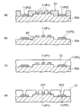
先ず最初の工程では(図2(a)参照)、仮基板としての支持基材60を用意する。この支持基材60の材料としては、後述するように最終的にはエッチングされることを考慮して、エッチング液で溶解可能な金属(典型的には、銅(Cu))が用いられる。また、支持基材60の形態としては、基本的には金属板もしくは金属箔で十分である。具体的には、例えば、プリプレグ(補強材のガラス布にエポキシ系樹脂、ポリイミド系樹脂等の熱硬化性樹脂を含浸させ、半硬化のBステージ状態にした接着シート)上に下地層及び銅箔を配置して加熱・加圧することにより得られた構造体(例えば、特開2007−158174号公報に開示された支持基材)を、支持基材60として使用することができる。
First, in the first step (see FIG. 2A), a
次の工程では(図2(b)参照)、支持基材60上に、パターニング材料を使用してエッチングレジストを形成し、所要の形状にパターニングしてレジスト層61を形成する。このレジスト層61は、最終的にチップ搭載面(パッケージ接合面)側の最外層の樹脂層12に形成されるキャビティCV(チップ搭載エリアCMよりも若干大きいサイズ)の位置に対応する部分のみが残存するようにパターニング形成される。
In the next step (see FIG. 2B), an etching resist is formed on the
パターニング材料としては、感光性のドライフィルム(レジスト材料をポリエステルのカバーシートとポリエチレンのセパレータシートの間に挟んだ構造のもの)、又は液状のフォトレジスト(ノボラック系樹脂、エポキシ系樹脂等の液状レジスト)を用いることができる。例えば、ドライフィルムを使用する場合には、支持基材60の表面を洗浄後、ドライフィルムを熱圧着により貼り付け、このドライフィルムを、所要の形状にパターニングされたマスク(図示せず)を用いて紫外線(UV)照射による露光を施して硬化させ、さらに所定の現像液を用いて当該部分以外の部分をエッチング除去し、所要のキャビティCVの形状に応じたレジスト層61を形成する。液状のフォトレジストを用いた場合も、同様の工程を経て、レジスト層61を形成することができる。
The patterning material can be a photosensitive dry film (with a resist material sandwiched between a polyester cover sheet and a polyethylene separator sheet), or a liquid photoresist (novolak resin, epoxy resin, or other liquid resist). ) Can be used. For example, when using a dry film, after cleaning the surface of the
次の工程では(図2(c)参照)、そのレジスト層(エッチングレジスト)61が形成された支持基材60に対し、そのエッチングレジスト61をマスクにして所要の深さにエッチングを施す。例えば、塩化第二鉄水溶液、塩化第二銅水溶液、過硫酸アンモニウム水溶液などを用いたウェットエッチングにより、支持基材(Cu)60を、レジスト層61に対して選択的に所要量だけ除去する。これにより、図示のようにそのエッチング量に応じた段差部SPを有する支持基材60aが形成される。
In the next step (see FIG. 2C), the
この支持基材60aの段差部SP(すなわち、エッチング量)は、形成すべきキャビティCVの深さを規定するので、搭載すべきチップの大きさやチップ搭載時にアンダーフィル樹脂を充填したときにその間隙から周囲に流れ出す樹脂の量などを適宜考慮して、エッチングの条件やエッチング時間等を適宜選択する必要がある。
The stepped portion SP (that is, the etching amount) of the
次の工程では(図2(d)参照)、エッチングレジストとして用いたレジスト層61を除去する。例えば、エッチングレジストとしてドライフィルムを使用した場合には、水酸化ナトリウムやモノエタノールアミン系などのアルカリ性の薬液を用いて除去することができ、ノボラック系樹脂、エポキシ系樹脂等の液状レジストを使用した場合には、アセトンやアルコール等を用いて除去することができる。これにより、図示のように所要の段差部SPを有した支持基材60aが形成れたことになる。
In the next step (see FIG. 2D), the resist
次の工程では(図2(e)参照)、支持基材60a上の段差部SP(図2(d))が形成されている側の面に、パターニング材料を使用してめっきレジストを形成し、その段差部SPの上の部分と下の部分にそれぞれ対応する部分において所要の箇所を開口する(開口部OP1及びOP2を備えたレジスト層62の形成)。開口部OP1及びOP2は、それぞれチップ搭載エリアCM内及びその周囲に対応する部分において、それぞれ形成すべき所要のパッドP1及びP2の形状に従ってパターニング形成される。パターニング材料としては、図2(b)の工程で使用した材料と同様に、感光性のドライフィルム又は液状のフォトレジストを用いることができる。
In the next step (see FIG. 2E), a plating resist is formed using a patterning material on the surface of the
次の工程では(図3(a)参照)、レジスト層62に開口された開口部OP1及びOP2(図2(e))から露出している支持基材(Cu)60a上に、この支持基材60aを給電層として利用した電解めっきにより、配線層11を形成する。この配線層11の所定の複数箇所に画定された各部分は、チップを搭載するためのパッドP1及び他のパッケージをPOP接合するためのパッドP2として機能する。
In the next step (see FIG. 3A), the support base is formed on the support base (Cu) 60a exposed from the openings OP1 and OP2 (FIG. 2E) opened in the resist
形成すべきパッドP1,P2は、特に図示はしないが、いずれも円形であり、それぞれの大きさ(直径)は、チップ搭載用のパッドP1については50〜150μm程度に選定され、他のパッケージ搭載用のパッドP2については200〜1000μm程度に選定される。また、各パッドP1,P2は、複数の金属層が積層された構造からなり、その最下層の金属層(最終的に露出する側の金属層)を構成する材料としては、これに接触する支持基材60aが最終的にエッチングされることを考慮して、そのエッチング液で溶解されない金属種を選定する。本実施形態では、支持基材60aの材料として銅(Cu)を用いているので、これとは異なる金属として、良好なコンタクト性(はんだ付け性)を確保できるという点を考慮し、金(Au)を使用している。
The pads P1 and P2 to be formed are not particularly shown, but both are circular, and the size (diameter) of each is selected to be about 50 to 150 μm for the chip mounting pad P1, and other packages are mounted. The pad P2 for use is selected to be about 200 to 1000 μm. Each of the pads P1 and P2 has a structure in which a plurality of metal layers are laminated, and the material constituting the lowermost metal layer (the metal layer that is finally exposed) is a support that comes into contact therewith. Considering that the
具体的には、先ず支持基材(Cu)60a上にAuフラッシュめっきを施して厚さ40nm程度のAu層を形成し、さらにパラジウム(Pd)フラッシュめっきを施して厚さ20nm程度のPd層を形成して、Au/Pd層を形成する。次いで、このAu/Pd層上にニッケル(Ni)めっきを施して厚さ5μm程度のNi層を形成し、さらにNi層上にCuめっきを施して厚さ15μm程度のCu層を形成する。ここに、Pd層は、その下層部分であるAu層の酸化を防止するために形成され、Ni層は、その上層の金属層に含まれるCuが下層のAu/Pd層に拡散するのを防止するために形成されている。 Specifically, first, Au flash plating is performed on the support base (Cu) 60a to form an Au layer having a thickness of about 40 nm, and further palladium (Pd) flash plating is applied to form a Pd layer having a thickness of about 20 nm. Then, an Au / Pd layer is formed. Next, nickel (Ni) plating is performed on the Au / Pd layer to form a Ni layer having a thickness of about 5 μm, and further Cu plating is performed on the Ni layer to form a Cu layer having a thickness of about 15 μm. Here, the Pd layer is formed to prevent oxidation of the Au layer which is the lower layer portion, and the Ni layer prevents Cu contained in the upper metal layer from diffusing into the lower Au / Pd layer. Is formed to do.
つまり、この工程では、Au/Pd層とNi層とCu層の3層(厳密には4層)構造からなるパッドP1,P2を形成している。なお、本工程では最下層の金属層としてAu/Pd層を形成しているが、Pd層については必ずしも形成する必要はなく、Au層のみからなる金属層としてもよい。 That is, in this step, pads P1 and P2 having a three-layer (strictly four-layer) structure of an Au / Pd layer, a Ni layer, and a Cu layer are formed. In this step, the Au / Pd layer is formed as the lowermost metal layer. However, the Pd layer is not necessarily formed, and may be a metal layer including only the Au layer.
次の工程では(図3(b)参照)、めっきレジストとして用いたレジスト層62を除去する。除去方法については、図2(d)の工程で説明した方法と同じである。これによって、図示のように支持基材60a上の段差部SPの上の部分及び下の部分にそれぞれパッドP1(配線層11)及びパッドP2(配線層11)が形成された構造体が作製されたことになる。
In the next step (see FIG. 3B), the resist
次の工程では(図3(c)参照)、支持基材60a上のパッドP1,P2が形成されている側の面に、エポキシ系樹脂やポリイミド系樹脂等からなる絶縁層12を形成する。例えば、エポキシ系樹脂フィルムを支持基材60a及びパッドP1,P2(配線層11)上にラミネートし、この樹脂フィルムをプレスしながら130〜150℃の温度で熱処理して硬化させることにより、樹脂層(絶縁層12)を形成することができる。この場合、支持基材60aの段差部SPと比べて樹脂フィルムの厚さは相対的に薄いため、1回のラミネートでは絶縁層12の表面の平坦性を確保するのは難しく、2回に分けて積層するのが望ましい。
In the next step (see FIG. 3C), the insulating
次の工程では(図3(d)参照)、この絶縁層12の所定の箇所(パッドP1,P2に対応する部分)に、炭酸ガスレーザ、エキシマレーザ等による穴明け処理により、それぞれパッドP1,P2に達する開口部(ビアホールVH1,VH2)を形成する。なお、本工程ではレーザ等によりビアホールVH1,VH2を形成しているが、絶縁層12が感光性樹脂を用いて形成されている場合には、フォトリソグラフィにより所要のビアホールを形成することも可能である。
In the next step (see FIG. 3D), pads P1 and P2 are respectively formed in predetermined portions of the insulating layer 12 (portions corresponding to the pads P1 and P2) by drilling with a carbon dioxide laser, an excimer laser, or the like. Openings (via holes VH1 and VH2) reaching to are formed. In this step, the via holes VH1 and VH2 are formed by a laser or the like. However, when the insulating
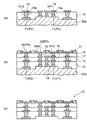
次の工程では(図4(a)参照)、ビアホールVH1,VH2が形成された絶縁層12上に、各ビアホールVH1,VH2をそれぞれ充填して(ビア13a,13bの形成)、各パッドP1,P2に接続される所要パターンの配線層14を形成する。この配線層14は、例えば、セミアディティブ法により形成される。
In the next step (see FIG. 4A), the via holes VH1 and VH2 are filled on the insulating
具体的には、先ず、無電解めっきやスパッタリング等により、ビアホールVH1,VH2の内部を含めて絶縁層12上に銅(Cu)のシード層(図示せず)を形成した後、形成すべき配線層14の形状に応じた開口部を備えたレジスト膜(図示せず)を形成する。次に、このレジスト膜の開口部から露出しているシード層(Cu)上に、このシード層を給電層として利用した電解Cuめっきにより、導体(Cu)パターン(図示せず)を形成する。さらに、レジスト膜を除去した後に、導体(Cu)パターンをマスクにしてシード層をエッチングすることで、所要の配線層14が得られる。
Specifically, first, a copper (Cu) seed layer (not shown) is formed on the insulating
なお、セミアディティブ法以外に、サブトラクティブ法など各種の配線形成方法を用いてもよい。また、ビア13a,13bの形成については、無電解めっき等に限らず、スクリーン印刷法を用いた導電性ペースト(銀ペースト、銅ペースト等)の充填によって形成することも可能である。
In addition to the semi-additive method, various wiring forming methods such as a subtractive method may be used. The
次の工程では(図4(b)参照)、図3(c)〜図4(a)の工程で行った処理と同様にして、絶縁層と配線層を交互に積層する。図示の例では、簡単化のため、2層の絶縁層と2層の配線層が積層されている。すなわち、絶縁層12及び配線層14上に樹脂層(絶縁層15)を形成し、この絶縁層15に、配線層14のパッド(図示せず)に達するビアホールVH3を形成した後、このビアホールVH3を充填して(ビア16の形成)当該パッドに接続される所要パターンの配線層17を形成する。さらに、絶縁層15及び配線層17上に樹脂層(絶縁層18)を形成し、この絶縁層18に、配線層17のパッド(図示せず)に達するビアホールVH4を形成した後、このビアホールVH4を充填して(ビア19の形成)当該パッドに接続される所要パターンの配線層20を形成する。この配線層20は、本実施形態では最外層の配線層を構成する。
In the next step (see FIG. 4B), insulating layers and wiring layers are alternately laminated in the same manner as the processing performed in the steps of FIGS. 3C to 4A. In the illustrated example, for the sake of simplicity, two insulating layers and two wiring layers are stacked. That is, a resin layer (insulating layer 15) is formed on the insulating
さらに、この配線層20の所定の箇所に画定されるパッドP3,P4の部分を除いて表面(絶縁層18及び配線層20)を覆うようにソルダレジスト層21を形成する。このソルダレジスト層21は、例えば、感光性のソルダレジストフィルムをラミネートし、又は液状のフォトレジストを塗布し、当該レジストを所要の形状にパターニングすることで形成することができる。これによって、ソルダレジスト層21の開口部からパッドP3,P4が露出する。
Further, a solder resist
これらパッドP3,P4には、本パッケージ10をマザーボード等に実装する際に使用されるはんだボールやピン等の外部接続端子が接合されるので、チップ搭載面(パッケージ接合面)側のパッドP1,P2と同様に、コンタクト性を良くするためにAuめっきを施しておくのが望ましい。その際、各パッド(Cu)P3,P4上にNiめっきを施してからAuめっきを施す。つまり、Ni層とAu層の2層構造からなる導体層(図示せず)を各パッドP3,P4上に形成する。
Since these pads P3 and P4 are connected to external connection terminals such as solder balls and pins used when the
最後の工程では(図4(c)参照)、仮基板として用いた支持基材60aを、パッドP1,P2、樹脂層12、パッドP3,P4及びソルダレジスト層21に対して選択的に除去する。例えば、塩化第二鉄水溶液、塩化第二銅水溶液、過硫酸アンモニウム水溶液などを用いたウェットエッチングにより、パッドP1,P2(各々の表層部にAu層が形成されている)、樹脂層12、パッドP3,P4(各々の表層部にAu層が形成されている)及びソルダレジスト層21に対して、支持基材(Cu)60aを選択的にエッチングして除去することができる。
In the last step (see FIG. 4C), the
以上の工程により、本実施形態の配線基板10(図1)が製造されたことになる。 The wiring board 10 (FIG. 1) of this embodiment is manufactured by the above process.
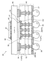
本実施形態の配線基板(半導体パッケージ)10には、上述したように一方の面から露出するパッドP1にチップの電極パッドがはんだバンプ等を介して接続されるとともに、パッドP2に他のパッケージの電極パッドがはんだバンプ等を介して接続され、他方の面から露出するパッドP3,P4にはんだボール等の外部接続端子が接合される。図5はその一構成例を示したものである。 In the wiring substrate (semiconductor package) 10 of the present embodiment, as described above, the electrode pads of the chip are connected to the pads P1 exposed from one surface via solder bumps or the like, and other packages are connected to the pads P2. The electrode pads are connected via solder bumps or the like, and external connection terminals such as solder balls are joined to the pads P3 and P4 exposed from the other surface. FIG. 5 shows an example of the configuration.
図5の例では、本パッケージ10に電子部品としての半導体素子(特定的には、CPU等の能動素子のチップ)31を搭載し、さらに他のパッケージ40を搭載した状態、すなわち、POP構造の半導体装置30を構成した場合の断面構造を示している。搭載されるチップ31は、その電極パッド(図示せず)がはんだバンプ32を介してキャビティCV内のパッドP1にフリップチップ接続されている。このようにキャビティCV内にチップ31を実質的に収容する形で搭載しているので、チップ31の表面は最外層の樹脂層12の表面から僅かに突出する程度である。
In the example of FIG. 5, a semiconductor element (specifically, a chip of an active element such as a CPU) 31 as an electronic component is mounted on the
さらに、その搭載されたチップ31と配線基板10(チップ31に対向する樹脂層12の面)との間隙にアンダーフィル樹脂33(熱硬化性のエポキシ系樹脂など)を充填し、熱硬化させて、チップ31と配線基板10との接続信頼性を高めている。樹脂充填後にチップ・基板間から溢れ出たアンダーフィル樹脂33は、図示のようにキャビティCV内で堰き止められている。つまり、チップ・基板間から周囲に流れ出したアンダーフィル樹脂33の「流れ出し」の範囲をキャビティCV内に止めておくことで、チップ周辺に配置されている回路素子や配線等(図示の例では、配線層11の一部に画定されたパッドP2)に悪影響が及ぼされるのを防いでいる。
Further, an underfill resin 33 (such as a thermosetting epoxy resin) is filled in a gap between the mounted
また、キャビティCVの周囲の樹脂層12上に露出するパッドP2には、他のパッケージ(配線基板)40の実装面側に形成された電極パッド(図示せず)がはんだバンプ34を介して接続されている(POP接続)。その接続の際、上述したようにチップ31の表面は樹脂層12の表面から僅かに突出する程度であるので、上下パッケージ40,10間の間隔は相対的に狭められ、その分だけはんだバンプ34の大きさを小さくすることができる。つまり、使用されるはんだ量を少なくできるので、従来技術に見られたような不都合(はんだの泣き別れやブリッジ等)が解消され、接続信頼性の向上に寄与する。
Further, an electrode pad (not shown) formed on the mounting surface side of another package (wiring substrate) 40 is connected to the pad P2 exposed on the
また、他のパッケージ40の実装面側と反対側の面(図示の例では上側)には、本パッケージ10と同様に半導体素子(チップ)41が搭載されている。このチップ41は、その電極パッド(図示せず)がはんだバンプ42を介してパッケージ40上のパッド(図示せず)にフリップチップ接続されている。さらに、その搭載されたチップ41とパッケージ40との間隙にアンダーフィル樹脂43が充填され、熱硬化されて、チップ41がパッケージ40に固定化されている。
Further, a semiconductor element (chip) 41 is mounted on the surface opposite to the mounting surface side of the other package 40 (upper side in the illustrated example), similarly to the
一方、本パッケージ10のチップ搭載面(パッケージ接合面)と反対側の外部接続端子接合面の各パッドP3,P4には、それぞれはんだボール35がリフローにより接合されている。図示の例では、パッドP3,P4にはんだボール35を接合したBGA(ボール・グリッド・アレイ)の形態としているが、これの代わりに、当該パッドにピンを接合したPGA(ピン・グリッド・アレイ)の形態や、当該パッド自体を外部接続端子としたLGA(ランド・グリッド・アレイ)の形態としてもよい。
On the other hand,
また、図5の設置態様とは逆に、チップ搭載面(パッケージ接合面)と外部接続端子接合面を上下反対に使用してPOP構造を実現することも可能である。図6はその一構成例を示したものである。 In contrast to the installation mode of FIG. 5, it is also possible to realize the POP structure by using the chip mounting surface (package bonding surface) and the external connection terminal bonding surface upside down. FIG. 6 shows an example of the configuration.
図6の例では、図5の場合とはパッケージの上下関係を逆にし、本パッケージ10を他のパッケージ50上に搭載してなるPOP構造の半導体装置30aの構成(断面構造)を示している。図6の構成例では、上記の能動素子(チップ31)の代わりに、受動素子としてのチップキャパシタ36がパッケージ10のキャビティCV内に搭載されている。このチップキャパシタ36は、その1対の電極端子(図示せず)がそれぞれはんだ37を用いて当該パッドP1に接続されている。この構成例においても、キャビティCV内にチップキャパシタ36を実質的に収容する形で搭載しているので、チップキャパシタ36の表面は最外層の樹脂層12の表面から僅かに突出する程度である。
The example of FIG. 6 shows the configuration (cross-sectional structure) of a POP
また、キャビティCVの周囲の樹脂層12上に露出するパッドP2には、他のパッケージ(配線基板)50の実装面側と反対側の面(図示の例では上側)に形成された電極パッド(図示せず)がはんだバンプ34を介して接続されている(POP接続)。その接続の際、上述したようにチップキャパシタ36の表面は樹脂層12の表面から僅かに突出する程度であり、上下パッケージ10,50間の間隔は相対的に狭められるので、その分だけはんだバンプ34の大きさを小さくする(使用されるはんだ量を少なくする)ことができる。これにより、従来技術に見られたようなはんだの泣き別れ等の不都合が解消され、POP接続の信頼性が高まる。
Further, the pad P2 exposed on the
また、他のパッケージ50の実装面側には電極パッド(図示せず)が設けられており、この電極パッドに、当該パッケージ50をマザーボード等に実装する際に使用される外部接続端子としてのはんだボール51がリフローにより接合されている。
In addition, an electrode pad (not shown) is provided on the mounting surface side of the
一方、本パッケージ10のチップ搭載面(パッケージ接合面)と反対側の外部接続端子接合面には、図5の構成におけるチップ31と同様の能動素子(チップ31a)が搭載されている。このチップ31aは、その電極パッド(図示せず)がはんだバンプ32aを介してパッケージ10上のパッドP3にフリップチップ接続されている。さらに、そのチップ31aとパッケージ10との間隙にアンダーフィル樹脂33aが充填され、熱硬化されて、チップ31aがパッケージ10に固定化されている。なお、図6の例では、パッケージ10の外部接続端子接合面側のパッドP4(図5)については図示を省略している。
On the other hand, an active element (
以上説明したように、本実施形態に係る配線基板(半導体パッケージ)10及びその製造方法(図1〜図4)によれば、チップ搭載面(パッケージ接合面)側の最外層の樹脂層12上のチップ搭載エリアCMに対応する箇所に、所要の深さにキャビティCVが形成され、このキャビティCV内の樹脂層12の表面と同一面にチップ搭載用のパッドP1の表面が位置し、かつ、キャビティCVの周囲の樹脂層12の表面と同一面にPOP接合用のパッドP2の表面が位置するように形成されている。このようにパッドP1が露出する樹脂層12の表面の高さを、パッドP2が露出する樹脂層12の表面よりも低くなるように形成しているので、図5、図6の構成例に示したようにPOP接続を容易に行うことができる。
As described above, according to the wiring substrate (semiconductor package) 10 and the manufacturing method (FIGS. 1 to 4) according to the present embodiment, the
すなわち、パッケージ10に搭載する電子部品(チップ31、チップキャパシタ36)をキャビティCV内に収容できるので、その周囲のパッドP2に接続される他のパッケージ40,50との間隔を相対的に狭くすることができる。このため、従来技術で使用されていたようなインターポーザを介在させなくても、その狭められた間隔に応じた少量のはんだ(はんだバンプ34)を介して上下パッケージ間の接続(POP接続)を容易に行うことが可能となる。つまり、POP接続を行うに際し、インターポーザが不要となることで、コストの低減化を図ることができる。
That is, since the electronic components (
また、POP接続を行う際、上下パッケージ間の間隔を小さくできるため、パッケージ間を接続するはんだ(バンプ)の使用量も少なくなる。その結果、従来技術に見られたようなはんだの泣き別れやブリッジ等の不都合が解消され、上下パッケージ間の接続信頼性が向上する。 In addition, since the interval between the upper and lower packages can be reduced when performing POP connection, the amount of solder (bump) used to connect the packages is reduced. As a result, inconveniences such as solder breaks and bridges as seen in the prior art are eliminated, and the connection reliability between the upper and lower packages is improved.
さらに、搭載するチップ31,36をキャビティCV内に収容できるので、パッケージ10の高さを相対的に低くすることができ、小型・薄型化に寄与する。その結果、POP構造全体として見た場合に、所望の小型・薄型化を達成することが可能となる。
Furthermore, since the
なお、図5、図6に示した構成例では、パッケージ10のキャビティCV内に搭載するチップ31,36の表面は樹脂層12の表面より僅かに突出しているが、キャビティCVの深さをさらに深く形成することにより、当該チップ全体をキャビティCV内に収容することができる。これにより、上下パッケージ間の間隔をさらに狭めることができ、更なる薄型化を図ることができる。また、それに応じて使用されるはんだ量も少なくなる。ただし、この場合、図2(c)の工程で行うエッチングの時間が長くなるため、このエッチング時間も考慮してキャビティCVの深さを適宜選定する必要がある。
5 and 6, the surfaces of the
また、チップの搭載面(パッドP1が露出する樹脂層12の表面)がキャビティCV内に位置しているので、図5に示したように樹脂充填後にチップ・基板間から溢れ出たアンダーフィル樹脂33の「流れ出し」を抑制することができる。つまり、キャビティCVをダムとして機能させることで、チップ周辺に配置されている配線や回路素子等に悪影響が及ぼされるのを防ぐことができる。
Further, since the chip mounting surface (the surface of the
また、キャビティCVの深さを適宜変えることで、最外層の樹脂層12の使用量を調整できるので、この樹脂層12とパッドP1,P2を構成する導体層との熱膨張係数の違いに起因して起こり得るパッケージ10の反りを抑制することができる。
Moreover, since the usage-amount of the
つまり、本パッケージ10は支持基材を含まないコアレス基板であり、剛性が小さく、その厚さも薄いため、反りが発生することが想定される。特に、チップ実装の際に行うリフロー等の熱処理や、チップ実装後に充填されるアンダーフィル樹脂の熱硬化等の熱履歴に晒されると、導体層と樹脂層の熱膨張係数の違い、さらにアンダーフィル樹脂とチップ材料の熱膨張係数の違いに起因して、パッケージ10に反りが発生する可能性が高い。そこで、上記のようにキャビティCVの深さ(樹脂層12の使用量)を適宜変えることで、パッケージ10の反りを抑制することが可能となる。
In other words, the
(第2の実施形態…図7参照)
図7は本発明の第2の実施形態に係る配線基板(半導体パッケージ)の構成を断面図の形態で示したものである。
(Second embodiment: see FIG. 7)
FIG. 7 shows the configuration of a wiring board (semiconductor package) according to the second embodiment of the present invention in the form of a sectional view.
この第2の実施形態に係る配線基板(半導体パッケージ)10aは、第1の実施形態に係る配線基板10(図1)の構成と比べて、キャビティCV内のチップ搭載エリアCMに配置されたパッドP1の表面が、そのキャビティCVの底面(樹脂層12aの表面)から所定の深さだけ基板内側に後退した位置となるように形成されている点で相違している。つまり、キャビティCV内において樹脂層12a上のパッドP1に対応する箇所に凹部DPが形成されている。他の構成については、図1の配線基板10の構成と基本的に同じであるのでその説明は省略する。
The wiring board (semiconductor package) 10a according to the second embodiment has pads arranged in the chip mounting area CM in the cavity CV, as compared with the configuration of the wiring board 10 (FIG. 1) according to the first embodiment. P1 is different in that the surface of P1 is formed so as to recede to the inside of the substrate by a predetermined depth from the bottom surface of the cavity CV (the surface of the
本実施形態に係る配線基板10aは、基本的には、上述した第1の実施形態に係る製造方法の各工程(図2〜図4)で行った処理と同様にして製造することができる。ただし、キャビティCV内の凹部DPを形成するための処理工程を必要とするため、これに関連する工程において行われる処理が若干異なる。特に図示はしないが、その製造方法の一例を説明すると、以下の通りである。
The
先ず、図2(a)〜(d)の工程を経て支持基材60aを形成した後、この支持基材60a上の段差部SPが形成されている側の面に、図2(e)の工程で行った処理と同様にして、パターニング材料を使用してめっきレジストを形成し、その段差部SPの上の部分の所要の箇所(形成すべきパッドP1に対応する部分)のみを開口する。つまり、開口部OP1のみを備えたレジスト層を形成する。
First, after forming the
次に、このレジスト層の開口部OP1から露出している支持基材60a上に、この支持基材60aを給電層として利用した電解めっきにより、犠牲導体層を所要の厚さ(形成すべき凹部DPの深さに相当する厚さ)に形成する。この犠牲導体層を構成する材料としては、これに接触する支持基材60aと共に最終的にエッチングされることを考慮して、そのエッチング液で溶解され得る金属種を選定する。この場合、支持基材60aの材料として銅(Cu)を用いているので、この支持基材60a上に電解Cuめっきを施して犠牲導体層(Cu)を形成する。このように同じ材料(Cu)を選定することで、最終的に1回のエッチングで各部材(支持基材60aと犠牲導体層)を同時に除去することができ、工程の簡素化に寄与する。
Next, a sacrificial conductor layer is formed on the
さらに、このめっきレジストを除去した後、支持基材60a上の犠牲導体層(Cu)が形成されている側の面に、図2(e)の工程で行った処理と同様にして、パターニング材料を使用してめっきレジストを形成し、その段差部SPの上の部分と下の部分にそれぞれ対応する部分において所要の箇所(パッドP1,P2に対応する部分)を開口する。つまり、図2(e)の工程におけるレジスト層62と同様のパターン形状を有したレジスト層を形成する。
Further, after removing the plating resist, the patterning material is formed on the surface of the
次に、図3(a)の工程で行った処理と同様にして、このレジスト層の開口部OP1及びOP2から露出している犠牲導体層(Cu)及び支持基材(Cu)60a上に、この支持基材60aを給電層として利用した電解めっきにより、Au/Pd層(又はAu層)、Ni層及びCu層を順次積層してパッドP1,P2を形成する。さらに、このめっきレジストを除去し、図3(c)〜図4(b)の各工程で行った処理と同様の処理を行った後、支持基材(Cu)60aと共に犠牲導体層(Cu)も併せてエッチングする。
Next, in the same manner as the process performed in the step of FIG. 3A, on the sacrificial conductor layer (Cu) and the support base material (Cu) 60a exposed from the openings OP1 and OP2 of the resist layer, The pads P1 and P2 are formed by sequentially laminating an Au / Pd layer (or Au layer), a Ni layer, and a Cu layer by electrolytic plating using the
以上の工程により、本実施形態の配線基板10a(図7)が製造されたことになる。
Through the above steps, the
なお、上述した製造方法では、最終段階でエッチングされる支持基材60aと犠牲導体層を同じ金属材(Cu)を用いて形成した場合を例にとって説明したが、両者は必ずしも同じ材料から形成される必要はない。要は、支持基材と犠牲導体層をそれぞれエッチングする際に、露出している他の構成部材に対して「選択的に」除去することができる材料で形成されていれば十分である。この場合、支持基材と犠牲導体層は互いに異なる材料から形成されることになるので、エッチング工程は2段階で行われる。
In the above-described manufacturing method, the case where the
本実施形態(図7)によれば、上述した実施形態(図1〜図6)で得られた効果に加えて、さらに以下の利点が得られる。すなわち、キャビティCV内において樹脂層12a上のパッドP1に対応する箇所に凹部DPが形成されているので、この凹部DPにプリソルダ(はんだ被着)を容易に施すことができ、POP接続(図5、図6)に先立って本パッケージ10aに電子部品(チップ)を接続する際に、チップの電極端子とその被着されたはんだとの位置合わせが行い易くなる。
According to this embodiment (FIG. 7), in addition to the effects obtained in the above-described embodiment (FIGS. 1 to 6), the following advantages are further obtained. That is, since the concave portion DP is formed at a location corresponding to the pad P1 on the
(第3の実施形態…図8参照)
図8は本発明の第3の実施形態に係る配線基板(半導体パッケージ)の構成を断面図の形態で示したものである。
(Third embodiment: see FIG. 8)
FIG. 8 shows a configuration of a wiring board (semiconductor package) according to the third embodiment of the present invention in the form of a sectional view.
この第3の実施形態に係る配線基板(半導体パッケージ)10bは、第1の実施形態に係る配線基板10(図1)の構成と比べて、キャビティCV内のチップ搭載エリアCMに配置されたパッドP1の表面が、そのキャビティCVの底面(樹脂層12bの表面)から所定の深さだけ基板内側に後退した位置となるように形成されると共に、キャビティCVの周囲の領域に配置されたパッドP2の表面も、樹脂層12bの表面から所定の深さだけ基板内側に後退した位置となるように形成されている点で相違している。つまり、キャビティCV内において樹脂層12b上のパッドP1に対応する箇所に凹部DP1が形成されると共に、キャビティCVの周囲の領域において樹脂層12b上のパッドP2に対応する箇所に凹部DP2が形成されている。他の構成については、図1の配線基板10の構成と基本的に同じであるのでその説明は省略する。
The wiring board (semiconductor package) 10b according to the third embodiment has pads arranged in the chip mounting area CM in the cavity CV, as compared with the configuration of the wiring board 10 (FIG. 1) according to the first embodiment. The surface of P1 is formed so as to be a position retracted from the bottom surface of the cavity CV (the surface of the
本実施形態に係る配線基板10bは、基本的には、上述した第1の実施形態に係る製造方法の各工程(図2〜図4)で行った処理と同様にして製造することができる。ただし、キャビティCV内の凹部DP1及びキャビティCVの周囲の凹部DP2を形成するための処理工程を必要とするため、これに関連する工程において行われる処理が若干異なる。特に図示はしないが、その製造方法の一例を説明すると、以下の通りである。
The
先ず、図2(a)〜(e)の工程で行った処理と同様にして、支持基材60a上の段差部SPが形成されている側の面に、その段差部SPの上の部分と下の部分にそれぞれ対応する部分に所要の開口部OP1及びOP2を備えためっきレジスト(レジスト層62)を形成する。
First, in the same manner as the processing performed in the steps of FIGS. 2A to 2E, the portion on the side of the
次に、このレジスト層62の開口部OP1,OP2から露出している支持基材(Cu)60a上に、この支持基材60aを給電層として利用した電解めっきにより、犠牲導体層を所要の厚さ(形成すべき凹部DP1,DP2の深さに相当する厚さ)に形成する。この犠牲導体層を構成する材料としては、これに接触する支持基材60aと共に最終的にエッチングされることを考慮して、そのエッチング液で溶解され得る金属種を選定する。この場合、支持基材60aの材料として銅(Cu)を用いているので、この支持基材60a上に電解Cuめっきを施して犠牲導体層(Cu)を形成する。このように同じ材料(Cu)を選定することで、最終的に1回のエッチングで各部材(支持基材60aと犠牲導体層)を同時に除去することができ、工程の簡素化に寄与する。
Next, a sacrificial conductor layer is formed on the support base (Cu) 60a exposed from the openings OP1 and OP2 of the resist
次に、図3(a)の工程で行った処理と同様にして、このレジスト層62の開口部OP1,OP2から露出している犠牲導体層(Cu)上に、支持基材60aを給電層として利用した電解めっきにより、それぞれAu/Pd層(又はAu層)、Ni層及びCu層を順次積層してパッドP1,P2を形成する。さらに、このレジスト層を除去し、図3(c)〜図4(b)の各工程で行った処理と同様の処理を行った後、支持基材(Cu)60aと共に犠牲導体層(Cu)も併せてエッチングする。
Next, in the same manner as the process performed in the step of FIG. 3A, the
以上の工程により、本実施形態の配線基板10b(図8)が製造されたことになる。
Through the above steps, the
なお、本実施形態においても第2の実施形態の場合と同様に、最終段階でエッチングされる支持基材60aと犠牲導体層は必ずしも同じ材料(Cu)から形成されている必要はない。要は、支持基材と犠牲導体層をそれぞれエッチングする際に、露出している他の構成部材に対して「選択的に」除去することができる材料で形成されていれば十分であり、両者は互いに異なる材料から形成されていてもよい。
In this embodiment as well, as in the case of the second embodiment, the
この第3の実施形態(図8)によれば、上述した第2の実施形態(図7)で得られた効果と同様の効果を奏することができる。すなわち、キャビティCV内の樹脂層12b上のパッドP1に対応する箇所に凹部DP1が形成されると共に、キャビティCVの周囲の領域において樹脂層12b上のパッドP2に対応する箇所に凹部DP2が形成されているので、各凹部DP1,DP2にプリソルダ(はんだ被着)を容易に施すことができる。これにより、本パッケージ10bに電子部品(チップ)を接続する際に、チップの電極端子とその被着されたはんだとの位置合わせが行い易くなり、さらにPOP接続(図5、図6)を行う際にも、他のパッケージの電極パッドとその被着されたはんだとの位置合わせが行い易くなる。
According to the third embodiment (FIG. 8), the same effect as that obtained in the second embodiment (FIG. 7) described above can be obtained. That is, the recess DP1 is formed at a location corresponding to the pad P1 on the
(他の実施形態)
上述した各実施形態では、パッケージ10(10a,10b)に電子部品(チップ)を収容するためのキャビティCVを、所要の形状にパターニングされたエッチングレジスト61(図2(c))をマスクにしてエッチングを施すことで形成した場合を例にとって説明したが、キャビティCVを形成する方法がこれに限定されないことはもちろんである。例えば、図2(b)の工程において、支持基材60上に形成すべきレジスト層を、図示のパターンとは逆のパターン(ポジとネガの関係)としためっきレジストとし、このめっきレジストを利用して所要のキャビティCVを形成することも可能である。
(Other embodiments)
In each of the above-described embodiments, the cavity CV for accommodating the electronic component (chip) in the package 10 (10a, 10b) is used as a mask with the etching resist 61 (FIG. 2C) patterned into a required shape. The case of forming by etching has been described as an example, but it goes without saying that the method of forming the cavity CV is not limited to this. For example, in the step of FIG. 2B, the resist layer to be formed on the
この場合、そのめっきレジストは、キャビティCV(チップ搭載エリアCMよりも若干大きいサイズ)の位置に対応する箇所に開口部を備えている。従って、このめっきレジストの開口部から露出している支持基材(Cu)60上に、この支持基材60を給電層として利用した電解Cuめっきにより、犠牲導体層(Cu)を所要の厚さ(キャビティCVの深さに相当する厚さ)に形成し、めっきレジストを除去後、図2(e)〜図4(b)の各工程で行った処理と同様の処理を経て、最終的に支持基材(Cu)と犠牲導体層(Cu)を同時にエッチングすることで、所望とするパッケージ10(10a,10b)を得ることができる。
In this case, the plating resist has an opening at a location corresponding to the position of the cavity CV (size slightly larger than the chip mounting area CM). Therefore, the sacrificial conductor layer (Cu) is formed on the supporting base material (Cu) 60 exposed from the opening of the plating resist by electrolytic Cu plating using the supporting
10,10a,10b…配線基板(半導体パッケージ)、
11,14,17,20…配線層、
12,12a,12b,15,18…樹脂層(絶縁層)、
13a,13b,16,19…ビア、
21…ソルダレジスト層(絶縁層)、
30,30a…半導体装置、
31,31a,36,41…半導体素子(チップ/電子部品)、
32,32a,34,37,42…はんだ(バンプ)、
33,33a,43…アンダーフィル樹脂、
60,60a…支持基材、
61,62…レジスト層、
CM…チップ搭載エリア、
CV…キャビティ、
DP,DP1,DP2…凹部、
P1,P2,P3,P4…パッド、
VH1,VH2,VH3,VH4…ビアホール。
10, 10a, 10b ... wiring board (semiconductor package),
11, 14, 17, 20 ... wiring layer,
12, 12a, 12b, 15, 18 ... resin layer (insulating layer),
13a, 13b, 16, 19 ... vias,
21 ... Solder resist layer (insulating layer),
30, 30a ... semiconductor device,
31, 31a, 36, 41 ... semiconductor element (chip / electronic component),
32, 32a, 34, 37, 42 ... solder (bump),
33, 33a, 43 ... Underfill resin,
60, 60a ... support substrate,
61, 62 ... resist layer,
CM: chip mounting area,
CV ... cavity,
DP, DP1, DP2 ... recess,
P1, P2, P3, P4 ... pad,
VH1, VH2, VH3, VH4 ... via holes.
Claims (5)
前記第1のレジスト層をマスクにして前記支持基材を所要量だけ除去し、段差部を有した支持基材を形成する工程と、
前記第1のレジスト層を除去後、前記支持基材の段差部が形成されている側の面に、該段差部の上の部分及び下の部分に対応する箇所にそれぞれ第1の開口部及び第2の開口部を有するようパターン形成された第2のレジスト層を形成する工程と、
前記第2のレジスト層の第1、第2の各開口部から露出している前記支持基材上に、それぞれ第1のパッド及び第2のパッドを形成する工程と、
前記第2のレジスト層を除去後、前記支持基材上に、前記第1、第2の各パッドを覆う絶縁層を形成する工程と、
前記絶縁層の上面から前記各パッドの一部を露出させる開口を形成する工程と、
前記絶縁層上に、前記各パッドにそれぞれ接続されるビアを含む配線層を形成する工程と、
以降、所要の層数となるまで絶縁層と配線層を交互に積層した後、前記支持基材を除去する工程とを含むことを特徴とする配線基板の製造方法。 Forming a first resist layer patterned so that only a portion corresponding to the position of the cavity to be formed remains on the support substrate;
Removing the supporting base material by a required amount using the first resist layer as a mask, and forming a supporting base material having a stepped portion;
After removing the first resist layer, a first opening and a portion corresponding to the upper part and the lower part of the step part are respectively formed on the surface of the support base on which the step part is formed. Forming a second resist layer patterned to have a second opening;
Forming a first pad and a second pad respectively on the support base exposed from the first and second openings of the second resist layer;
Forming an insulating layer covering each of the first and second pads on the support substrate after removing the second resist layer;
Forming an opening exposing a part of each pad from the upper surface of the insulating layer;
Forming a wiring layer including vias respectively connected to the pads on the insulating layer;
Thereafter, the method includes the step of alternately laminating the insulating layers and the wiring layers until the required number of layers is reached, and then removing the support base material.
前記第1のレジスト層の開口部から露出している前記支持基材上に、犠牲導体層を所要の厚さに形成して、段差部を有した支持基材を形成する工程と、
前記第1のレジスト層を除去後、前記支持基材の段差部が形成されている側の面に、該段差部の上の部分の犠牲導体層上及び該段差部の下の部分に対応する箇所にそれぞれ第1の開口部及び第2の開口部を有するようパターン形成された第2のレジスト層を形成する工程と、
前記第2のレジスト層の第1、第2の各開口部から露出している前記犠牲導体層及び前記支持基材上に、それぞれ第1のパッド及び第2のパッドを形成する工程と、
前記第2のレジスト層を除去後、前記犠牲導体層及び前記支持基材上に、前記第1、第2の各パッドを露出させて絶縁層を形成する工程と、
前記絶縁層の上面から前記各パッドの一部を露出させる開口を形成する工程と、
前記絶縁層上に、前記各パッドにそれぞれ接続されるビアを含む配線層を形成する工程と、
以降、所要の層数となるまで絶縁層と配線層を交互に積層した後、前記支持基材及び前記犠牲導体層を除去する工程とを含むことを特徴とする配線基板の製造方法。 Forming a first resist layer patterned to have an opening at a location corresponding to the position of the cavity to be formed on the support substrate;
Forming a sacrificial conductor layer in a required thickness on the support substrate exposed from the opening of the first resist layer to form a support substrate having a stepped portion;
After removing the first resist layer, the surface of the support base on which the step portion is formed corresponds to a portion above the sacrificial conductor layer above the step portion and a portion below the step portion. Forming a second resist layer that is patterned to have a first opening and a second opening at each location;
Forming a first pad and a second pad respectively on the sacrificial conductor layer and the support substrate exposed from the first and second openings of the second resist layer;
Forming the insulating layer by exposing the first and second pads on the sacrificial conductor layer and the support substrate after removing the second resist layer;
Forming an opening exposing a part of each pad from the upper surface of the insulating layer;
Forming a wiring layer including vias respectively connected to the pads on the insulating layer;
Thereafter, after the insulating layers and the wiring layers are alternately laminated until the required number of layers is obtained, the method for manufacturing the wiring board includes the step of removing the supporting base material and the sacrificial conductor layer.
前記キャビティ内の前記絶縁層の表面に露出する第1のパッドと、
前記キャビティの周囲の前記絶縁層の表面に露出する第2のパッドとを備えたことを特徴とする配線基板。 A cavity is formed at the location corresponding to the mounting area of the electronic component in the outermost insulating layer on one side,
A first pad exposed on a surface of the insulating layer in the cavity;
And a second pad exposed on the surface of the insulating layer around the cavity.
Priority Applications (2)
| Application Number | Priority Date | Filing Date | Title |
|---|---|---|---|
| JP2008317410A JP5026400B2 (en) | 2008-12-12 | 2008-12-12 | Wiring board and manufacturing method thereof |
| US12/628,281 US8067695B2 (en) | 2008-12-12 | 2009-12-01 | Wiring board and method of manufacturing the same |
Applications Claiming Priority (1)
| Application Number | Priority Date | Filing Date | Title |
|---|---|---|---|
| JP2008317410A JP5026400B2 (en) | 2008-12-12 | 2008-12-12 | Wiring board and manufacturing method thereof |
Publications (3)
| Publication Number | Publication Date |
|---|---|
| JP2010141204A true JP2010141204A (en) | 2010-06-24 |
| JP2010141204A5 JP2010141204A5 (en) | 2011-10-27 |
| JP5026400B2 JP5026400B2 (en) | 2012-09-12 |
Family
ID=42239171
Family Applications (1)
| Application Number | Title | Priority Date | Filing Date |
|---|---|---|---|
| JP2008317410A Active JP5026400B2 (en) | 2008-12-12 | 2008-12-12 | Wiring board and manufacturing method thereof |
Country Status (2)
| Country | Link |
|---|---|
| US (1) | US8067695B2 (en) |
| JP (1) | JP5026400B2 (en) |
Cited By (6)
| Publication number | Priority date | Publication date | Assignee | Title |
|---|---|---|---|---|
| JP2012195447A (en) * | 2011-03-16 | 2012-10-11 | Shinko Electric Ind Co Ltd | Wiring board and manufacturing method of the same |
| JP2013115290A (en) * | 2011-11-30 | 2013-06-10 | Fujitsu Semiconductor Ltd | Semiconductor device and semiconductor device manufacturing method |
| JP2015165533A (en) * | 2014-03-03 | 2015-09-17 | 新光電気工業株式会社 | Wiring board, method of manufacturing the same, and semiconductor device |
| US11382213B2 (en) | 2020-10-30 | 2022-07-05 | Samsung Electro-Mechanics Co., Ltd. | Printed circuit board |
| JP2023539243A (en) * | 2020-08-24 | 2023-09-13 | テキサス インスツルメンツ インコーポレイテッド | Electronic device inside semiconductor package cavity |
| US12575027B2 (en) | 2023-09-01 | 2026-03-10 | Samsung Electro-Mechanics Co., Ltd. | Printed circuit board |
Families Citing this family (38)
| Publication number | Priority date | Publication date | Assignee | Title |
|---|---|---|---|---|
| KR101019161B1 (en) * | 2008-12-11 | 2011-03-04 | 삼성전기주식회사 | Package substrate |
| JP5290215B2 (en) * | 2010-02-15 | 2013-09-18 | ルネサスエレクトロニクス株式会社 | Semiconductor device, semiconductor package, interposer, and manufacturing method of interposer |
| US20120152606A1 (en) * | 2010-12-16 | 2012-06-21 | Ibiden Co., Ltd. | Printed wiring board |
| US8466559B2 (en) | 2010-12-17 | 2013-06-18 | Intel Corporation | Forming die backside coating structures with coreless packages |
| CN102548253B (en) * | 2010-12-28 | 2013-11-06 | 富葵精密组件(深圳)有限公司 | Manufacturing method of multilayer circuit board |
| JP2014072372A (en) * | 2012-09-28 | 2014-04-21 | Ibiden Co Ltd | Printed wiring board manufacturing method and printed wiring board |
| US9275925B2 (en) | 2013-03-12 | 2016-03-01 | Taiwan Semiconductor Manufacturing Company, Ltd. | System and method for an improved interconnect structure |
| US9263376B2 (en) * | 2013-04-15 | 2016-02-16 | Intel Deutschland Gmbh | Chip interposer, semiconductor device, and method for manufacturing a semiconductor device |
| TW201503777A (en) * | 2013-05-30 | 2015-01-16 | 京瓷Slc技術股份有限公司 | Wiring substrate |
| JP2015035496A (en) * | 2013-08-09 | 2015-02-19 | イビデン株式会社 | Method of manufacturing electronic component built-in wiring board |
| KR20150021342A (en) * | 2013-08-20 | 2015-03-02 | 삼성전기주식회사 | Multi Layered Printed Circuit Board |
| US9159670B2 (en) | 2013-08-29 | 2015-10-13 | Qualcomm Incorporated | Ultra fine pitch and spacing interconnects for substrate |
| US9622350B2 (en) * | 2013-09-28 | 2017-04-11 | Intel Corporation | Method of forming a circuit board |
| TWI666749B (en) * | 2014-02-19 | 2019-07-21 | Siliconware Precision Industries Co., Ltd. | Package substrate and package structure |
| TW201539596A (en) * | 2014-04-09 | 2015-10-16 | 同欣電子工業股份有限公司 | Intermediary and manufacturing method thereof |
| US9609751B2 (en) * | 2014-04-11 | 2017-03-28 | Qualcomm Incorporated | Package substrate comprising surface interconnect and cavity comprising electroless fill |
| TWI504320B (en) * | 2014-06-17 | 2015-10-11 | 矽品精密工業股份有限公司 | A circuit structure and fabricating method thereof |
| TWI611523B (en) * | 2014-09-05 | 2018-01-11 | 矽品精密工業股份有限公司 | Semiconductor package manufacturing method |
| TWI551207B (en) * | 2014-09-12 | 2016-09-21 | 矽品精密工業股份有限公司 | Substrate structure and fabrication method thereof |
| US20160093567A1 (en) * | 2014-09-26 | 2016-03-31 | Qualcomm Incorporated | System, apparatus, and method of interconnection in a substrate |
| JP2016162835A (en) * | 2015-02-27 | 2016-09-05 | イビデン株式会社 | Multilayer wiring board |
| KR102340053B1 (en) * | 2015-06-18 | 2021-12-16 | 삼성전기주식회사 | Printed circuit board and method of manufacturing the same |
| CN104966709B (en) | 2015-07-29 | 2017-11-03 | 恒劲科技股份有限公司 | Package substrate and manufacturing method thereof |
| JP2017084997A (en) * | 2015-10-29 | 2017-05-18 | イビデン株式会社 | Printed wiring board and method of manufacturing the same |
| CN107424973B (en) * | 2016-05-23 | 2020-01-21 | 凤凰先驱股份有限公司 | Package substrate and its manufacturing method |
| WO2018004686A1 (en) * | 2016-07-01 | 2018-01-04 | Intel Corporation | Device, method and system for providing recessed interconnect structures of a substrate |
| US11272619B2 (en) * | 2016-09-02 | 2022-03-08 | Intel Corporation | Apparatus with embedded fine line space in a cavity, and a method for forming the same |
| TWI595812B (en) * | 2016-11-30 | 2017-08-11 | 欣興電子股份有限公司 | Circuit board structure and manufacturing method thereof |
| US9997442B1 (en) * | 2016-12-14 | 2018-06-12 | Advanced Semiconductor Engineering, Inc. | Semiconductor device and method of manufacturing the same |
| JP6789886B2 (en) * | 2017-06-09 | 2020-11-25 | 株式会社東芝 | Electronic device |
| CN109803481B (en) * | 2017-11-17 | 2021-07-06 | 英业达科技有限公司 | Multilayer printed circuit board and method for manufacturing multilayer printed circuit board |
| EP3849286B1 (en) * | 2020-01-09 | 2025-08-27 | Murata Manufacturing Co., Ltd. | Electronic device with differential transmission lines equipped with 3d capacitors supported by a base, and corresponding manufacturing method |
| KR102876502B1 (en) | 2020-07-09 | 2025-10-23 | 삼성전자주식회사 | Semiconductor package including interposer and method of manufacturing the semiconductor package |
| US20220069489A1 (en) * | 2020-08-28 | 2022-03-03 | Unimicron Technology Corp. | Circuit board structure and manufacturing method thereof |
| KR102921311B1 (en) * | 2020-12-01 | 2026-02-02 | 삼성전자주식회사 | Semiconductor packages having supporting members |
| JP7711870B2 (en) * | 2021-10-19 | 2025-07-23 | 新光電気工業株式会社 | Wiring board and manufacturing method thereof |
| TWI803312B (en) * | 2021-12-23 | 2023-05-21 | 南亞科技股份有限公司 | Semiconductor device with multi-stacking carrier structure |
| JP2023125724A (en) | 2022-02-28 | 2023-09-07 | 新光電気工業株式会社 | Wiring board and its manufacturing method |
Family Cites Families (5)
| Publication number | Priority date | Publication date | Assignee | Title |
|---|---|---|---|---|
| US6281446B1 (en) * | 1998-02-16 | 2001-08-28 | Matsushita Electric Industrial Co., Ltd. | Multi-layered circuit board and method of manufacturing the same |
| EP1990833A3 (en) * | 2000-02-25 | 2010-09-29 | Ibiden Co., Ltd. | Multilayer printed circuit board and multilayer printed circuit board manufacturing method |
| JP3709882B2 (en) * | 2003-07-22 | 2005-10-26 | 松下電器産業株式会社 | Circuit module and manufacturing method thereof |
| KR100792352B1 (en) | 2006-07-06 | 2008-01-08 | 삼성전기주식회사 | Bottom substrate of package on package and manufacturing method thereof |
| TWI335643B (en) * | 2006-11-21 | 2011-01-01 | Unimicron Technology Crop | Circuit board structure having embedded semiconductor chip and fabrication method thereof |
-
2008
- 2008-12-12 JP JP2008317410A patent/JP5026400B2/en active Active
-
2009
- 2009-12-01 US US12/628,281 patent/US8067695B2/en active Active
Cited By (7)
| Publication number | Priority date | Publication date | Assignee | Title |
|---|---|---|---|---|
| JP2012195447A (en) * | 2011-03-16 | 2012-10-11 | Shinko Electric Ind Co Ltd | Wiring board and manufacturing method of the same |
| US9078384B2 (en) | 2011-03-16 | 2015-07-07 | Shinko Electric Industries Co., Ltd. | Wiring substrate and method of manufacturing the same |
| JP2013115290A (en) * | 2011-11-30 | 2013-06-10 | Fujitsu Semiconductor Ltd | Semiconductor device and semiconductor device manufacturing method |
| JP2015165533A (en) * | 2014-03-03 | 2015-09-17 | 新光電気工業株式会社 | Wiring board, method of manufacturing the same, and semiconductor device |
| JP2023539243A (en) * | 2020-08-24 | 2023-09-13 | テキサス インスツルメンツ インコーポレイテッド | Electronic device inside semiconductor package cavity |
| US11382213B2 (en) | 2020-10-30 | 2022-07-05 | Samsung Electro-Mechanics Co., Ltd. | Printed circuit board |
| US12575027B2 (en) | 2023-09-01 | 2026-03-10 | Samsung Electro-Mechanics Co., Ltd. | Printed circuit board |
Also Published As
| Publication number | Publication date |
|---|---|
| JP5026400B2 (en) | 2012-09-12 |
| US20100147560A1 (en) | 2010-06-17 |
| US8067695B2 (en) | 2011-11-29 |
Similar Documents
| Publication | Publication Date | Title |
|---|---|---|
| JP5026400B2 (en) | Wiring board and manufacturing method thereof | |
| JP5221315B2 (en) | Wiring board and manufacturing method thereof | |
| JP5210839B2 (en) | Wiring board and manufacturing method thereof | |
| JP5711472B2 (en) | WIRING BOARD, MANUFACTURING METHOD THEREOF, AND SEMICONDUCTOR DEVICE | |
| JP5147779B2 (en) | Wiring board manufacturing method and semiconductor package manufacturing method | |
| JP3813402B2 (en) | Manufacturing method of semiconductor device | |
| JP5649490B2 (en) | Wiring board and manufacturing method thereof | |
| JP6076653B2 (en) | Electronic component built-in substrate and manufacturing method of electronic component built-in substrate | |
| JP5339928B2 (en) | Wiring board and manufacturing method thereof | |
| KR102331611B1 (en) | Electronic component device and method for manufacturing the same | |
| JP4619223B2 (en) | Semiconductor package and manufacturing method thereof | |
| US9935053B2 (en) | Electronic component integrated substrate | |
| JP2005217225A (en) | Semiconductor device and manufacturing method thereof | |
| JP2010245280A (en) | Wiring board manufacturing method and wiring board | |
| JP2005209689A (en) | Semiconductor device and manufacturing method thereof | |
| JP2009135162A (en) | Wiring board and electronic component device | |
| JP2008282842A (en) | Wiring board and manufacturing method thereof | |
| JP6550260B2 (en) | Wiring board and method of manufacturing wiring board | |
| JP2017163027A (en) | WIRING BOARD, SEMICONDUCTOR DEVICE, AND WIRING BOARD MANUFACTURING METHOD | |
| JP2012235166A (en) | Wiring board and manufacturing method of the same | |
| KR20190136240A (en) | Package board and method of manufacturing the same | |
| JP5315447B2 (en) | Wiring board and manufacturing method thereof | |
| JP2006049762A (en) | Component built-in substrate and method for manufacturing component built-in substrate | |
| JP2010067888A (en) | Wiring board and method of manufacturing the same | |
| JP3800215B2 (en) | Printed wiring board, semiconductor device, and manufacturing method thereof |
Legal Events
| Date | Code | Title | Description |
|---|---|---|---|
| A521 | Request for written amendment filed |
Free format text: JAPANESE INTERMEDIATE CODE: A523 Effective date: 20110908 |
|
| A621 | Written request for application examination |
Free format text: JAPANESE INTERMEDIATE CODE: A621 Effective date: 20110908 |
|
| A977 | Report on retrieval |
Free format text: JAPANESE INTERMEDIATE CODE: A971007 Effective date: 20120524 |
|
| TRDD | Decision of grant or rejection written | ||
| A01 | Written decision to grant a patent or to grant a registration (utility model) |
Free format text: JAPANESE INTERMEDIATE CODE: A01 Effective date: 20120619 |
|
| A01 | Written decision to grant a patent or to grant a registration (utility model) |
Free format text: JAPANESE INTERMEDIATE CODE: A01 |
|
| A61 | First payment of annual fees (during grant procedure) |
Free format text: JAPANESE INTERMEDIATE CODE: A61 Effective date: 20120620 |
|
| FPAY | Renewal fee payment (event date is renewal date of database) |
Free format text: PAYMENT UNTIL: 20150629 Year of fee payment: 3 |
|
| R150 | Certificate of patent or registration of utility model |
Ref document number: 5026400 Country of ref document: JP Free format text: JAPANESE INTERMEDIATE CODE: R150 Free format text: JAPANESE INTERMEDIATE CODE: R150 |