JP2010134027A - Wavelength selection switch - Google Patents
Wavelength selection switch Download PDFInfo
- Publication number
- JP2010134027A JP2010134027A JP2008307487A JP2008307487A JP2010134027A JP 2010134027 A JP2010134027 A JP 2010134027A JP 2008307487 A JP2008307487 A JP 2008307487A JP 2008307487 A JP2008307487 A JP 2008307487A JP 2010134027 A JP2010134027 A JP 2010134027A
- Authority
- JP
- Japan
- Prior art keywords
- light
- optical
- medium
- optical system
- wavelength selective
- Prior art date
- Legal status (The legal status is an assumption and is not a legal conclusion. Google has not performed a legal analysis and makes no representation as to the accuracy of the status listed.)
- Pending
Links
Images


Landscapes
- Mechanical Light Control Or Optical Switches (AREA)
Abstract
Description
本発明は、波長選択スイッチに関するものである。 The present invention relates to a wavelength selective switch.
従来、波長選択スイッチとして、例えば特許文献1、特許文献2に提案されたものが知られている。特許文献1には、透過型の波長選択スイッチが提案されている。また、特許文献2には、反射型の波長選択スイッチが提案されている。 Conventionally, as wavelength selective switches, for example, those proposed in Patent Document 1 and Patent Document 2 are known. Patent Document 1 proposes a transmission-type wavelength selective switch. Patent Document 2 proposes a reflective wavelength selective switch.
波長選択スイッチの光学系においては、小型化が求められている。波長選択スイッチの光学系の大きさを決めるパラメータのひとつに、分散素子と偏向素子に挟まられた光学系の焦点距離がある。この光学系の焦点距離をfとする。入力ポートから光学系に出射されたビームのビームウェストは、分散素子近傍、偏向素子近傍にそれぞれリレーされる構成が望ましい。 The optical system of the wavelength selective switch is required to be downsized. One of the parameters that determine the size of the optical system of the wavelength selective switch is the focal length of the optical system sandwiched between the dispersion element and the deflection element. Let the focal length of this optical system be f. It is desirable that the beam waist of the beam emitted from the input port to the optical system is relayed in the vicinity of the dispersive element and the deflecting element.
このとき、図6に示すように、分散素子から光学系801の主面までの距離、光学系801の主面から偏向素子までの距離を、それぞれ焦点距離fに設定すると、分散素子近傍にあるビームウェストが偏向素子近傍にリレーされる。
ここで、分散素子として反射型グレーティング810を使用し、偏向素子としてMEMSミラーアレイを使用する場合を仮定する。なお、図6では、説明の便宜上、反射型グレーティング810を透過型グレーティングとして描いている。
At this time, as shown in FIG. 6, if the distance from the dispersive element to the main surface of the
Here, it is assumed that a
反射型グレーティング810により、振動数が隣り合う2つの信号光の回折後の角度差をΔθ、MEMSミラーアレイ802の各マイクロミラーMどうしのピッチをpmとするとき、次式が正立する。
pm=f・Δθ …(1)
When the
pm = f · Δθ (1)
一般的に、分散素子として使われるpg=1000本/mm、すなわちpg=1μmの反射型グレーティングを例にとる(pgはグレーティングのピッチをあらわす)。Cバンド100GHzスペーシングの2つの波長193.9THzと194.0THzの信号光が、前述の1000本/mmのグレーティングに入射角50度で入射したとする。このとき、回折角はそれぞれ、51.229度、51.157度となる。このため、Δθ=0.0722度=0.000126radである(図7参照)。 In general, a reflective grating of pg = 1000 lines / mm, that is, pg = 1 μm, used as a dispersion element is taken as an example (pg represents the pitch of the grating). It is assumed that signal lights having two wavelengths of 193.9 THz and 194.0 THz with a C-band 100 GHz spacing are incident on the above-mentioned 1000 lines / mm grating at an incident angle of 50 degrees. At this time, the diffraction angles are 51.229 degrees and 51.157 degrees, respectively. Therefore, Δθ = 0.0722 degrees = 0.000126 rad (see FIG. 7).
文献(IEEE/LEOS OPTICAL MEMS 2004 32ページ A High-Speed Comb-Driven Micromirror Array for 1xN 80-channel Wavelength Selective Switches)で報告されているように、マイクロミラーのピッチpm=80μmである波長選択スイッチ用のMEMSミラーを用いるとき、焦点距離fは上記式(1)より63.46mmとなる。
以上のことを表1に掲げる。
As reported in the literature (IEEE / LEOS OPTICAL MEMS 2004 Page 32 A High-Speed Comb-Driven Micromirror Array for 1xN 80-channel Wavelength Selective Switches) When the MEMS mirror is used, the focal length f is 63.46 mm from the above formula (1).
The above is listed in Table 1.

したがって、波長選択スイッチの光学系が透過型であれば、分散素子から偏向素子までの距離が最低でも125mm程度になる。これでは、小型の波長選択スイッチを得ることはできない。また、波長選択スイッチの光学系が反射型のときも、分散素子から反射鏡までの距離が60mmを超える大きさとなる。 Therefore, if the optical system of the wavelength selective switch is a transmissive type, the distance from the dispersion element to the deflecting element is at least about 125 mm. With this, a small wavelength selective switch cannot be obtained. In addition, when the optical system of the wavelength selective switch is a reflection type, the distance from the dispersive element to the reflecting mirror exceeds 60 mm.
さらに、両方のタイプの波長選択スイッチに共通して、光束径が光学系の焦点距離に比例する。このため、この点からも小型化の妨げになっている。 Further, in common with both types of wavelength selective switches, the beam diameter is proportional to the focal length of the optical system. For this reason, this also hinders miniaturization.
本発明は上記に鑑みてなされたもので、より小型の波長選択スイッチを提供することを目的とする。 The present invention has been made in view of the above, and an object thereof is to provide a more compact wavelength selective switch.
上述した課題を解決し、目的を達成するために、本発明の波長選択スイッチは、
ファイバの端面で構成されている、光が出射する出射部と、
該光学系の出光出射側に配置された分散素子と、
前記分散素子の光出射側に配置された光偏向部材と、
ファイバの端面で構成されている、前記光偏向部材からの光が入射する入射部と、
前記出射部との光出射側に配置された光学系と、
前記出射部と前記光偏向部材との間の光路中に設けられている第1の光学系と、
前記分散素子と前記光偏向部材との光路中に設けられている第2の光学系とを有し、
前記分散素子は前記第2の光学系の前側焦点位置に設けられ、
前記光偏向部材は前記第2の光学系の後側焦点位置に設けられ、
前記光偏向部材は複数の偏向素子で構成され、
該複数の偏向素子は、互いに独立して制御可能であり、
前記分散素子は、光が透過する透過面と、
回折光学面を有し、
前記透過面から前記回折光学面までの間が、屈折率が1よりも大きい媒質で形成されていることを特徴とする。
In order to solve the above-described problems and achieve the object, the wavelength selective switch of the present invention includes:
An emission part configured by an end face of the fiber and emitting light;
A dispersive element disposed on the light output side of the optical system;
A light deflection member disposed on the light exit side of the dispersion element;
An incident part configured by an end face of a fiber and receiving light from the light deflection member;
An optical system disposed on the light emitting side with the emitting portion;
A first optical system provided in an optical path between the emitting portion and the light deflection member;
A second optical system provided in an optical path between the dispersion element and the light deflection member;
The dispersive element is provided at a front focal position of the second optical system;
The light deflection member is provided at a rear focal position of the second optical system;
The light deflection member is composed of a plurality of deflection elements,
The plurality of deflection elements can be controlled independently of each other,
The dispersion element includes a transmission surface through which light is transmitted;
Having a diffractive optical surface,
A portion between the transmission surface and the diffractive optical surface is formed of a medium having a refractive index larger than 1.
また、本発明の好ましい態様によれば、
前記透過面とは別の透過面を備え、
前記透過面は前記光が入射する入射面であり、
前記別の透過面は前記光が出射する出射面であり、
前記回折光学面は、前記入射面から前記出射面に至る光路中に配置され、
前記回折光学面は反射面であることが望ましい。
According to a preferred embodiment of the present invention,
A transmission surface different from the transmission surface,
The transmission surface is an incident surface on which the light is incident,
The another transmission surface is an emission surface from which the light is emitted,
The diffractive optical surface is disposed in an optical path from the incident surface to the exit surface,
The diffractive optical surface is preferably a reflective surface.
また、本発明の好ましい態様によれば、
前記分散素子は1つの前記媒質を備え、
前記入射面、前記出射面及び前記回折光学面は、1つの前記媒質に一体に形成されていることが望ましい。
According to a preferred embodiment of the present invention,
The dispersive element comprises one medium;
It is desirable that the entrance surface, the exit surface, and the diffractive optical surface are integrally formed on one medium.
また、本発明の好ましい態様によれば、
前記分散素子は前記媒質として第1の媒質と第2の媒質を備え、
前記入射面と前記出射面は前記第1の媒質に形成され、
前記回折光学面は、前記第2の媒質に形成されていることが望ましい。
According to a preferred embodiment of the present invention,
The dispersion element includes a first medium and a second medium as the medium,
The entrance surface and the exit surface are formed in the first medium,
The diffractive optical surface is preferably formed on the second medium.
また、本発明の好ましい態様によれば、前記媒質の屈折率が、1.8以上であることが望ましい。 According to a preferred aspect of the present invention, it is desirable that the refractive index of the medium is 1.8 or more.
また、本発明の好ましい態様によれば、前記媒質がシリコンであることが望ましい。 According to a preferred aspect of the present invention, it is desirable that the medium is silicon.
また、本発明の好ましい態様によれば、前記第2の光学系は、レンズであることが望ましい。 According to a preferred aspect of the present invention, it is desirable that the second optical system is a lens.
また、本発明の好ましい態様によれば、前記第2の光学系は、凹面鏡であることが望ましい。 According to a preferred aspect of the present invention, it is desirable that the second optical system is a concave mirror.
本発明によれば、より小型な波長選択スイッチを提供することができる。 According to the present invention, a more compact wavelength selective switch can be provided.
まず、初めに本発明に係る波長選択スイッチに用いる分散素子について説明する。次に、この分散素子を備える波長選択スイッチについて説明する。 First, the dispersion element used for the wavelength selective switch according to the present invention will be described. Next, a wavelength selective switch including this dispersion element will be described.
まずは、図8(b)をもとに、分散素子における媒質中の分散を考える。入射面は入射光線に対して垂直で、回折面への入射角は図7と同様とする。媒質800中の波長は、大気中の波長λを媒質の屈折率nで除してλ/nとなっている。したがって回折面Gのピッチをpgからpg/nに小さくすれば、媒質800中においては、図7を用いて説明した例と同様の分散が得られる。 First, based on FIG. 8B, the dispersion in the medium in the dispersion element is considered. The incident surface is perpendicular to the incident light, and the incident angle on the diffractive surface is the same as in FIG. The wavelength in the medium 800 is λ / n by dividing the wavelength λ in the atmosphere by the refractive index n of the medium. Therefore, if the pitch of the diffractive surface G is reduced from pg to pg / n, dispersion similar to the example described with reference to FIG.
次に、図8(a)をもとに、この光線が大気中に戻ることを考える。分散素子からの出射面(前述の入射面と同一)においてはスネルの法則に従い屈折を起こす。すなわち、次式(2)が成立する。
nsinθ1 = sinθ2 … (2)
Next, based on FIG. 8A, consider that this light beam returns to the atmosphere. Refraction occurs at the exit surface from the dispersive element (same as the aforementioned entrance surface) in accordance with Snell's law. That is, the following expression (2) is established.
nsinθ1 = sinθ2 (2)
ここで、θ1は出射面への入射角、θ2は出射面からの出射角である。この例ではθ1,θ2がともに小さいとみなせるので、sinθ≒θの近似が成り立つとして、式(2)は、式(3)と近似できる。
nθ1 = θ2 …(3)
Here, θ1 is an incident angle on the exit surface, and θ2 is an exit angle from the exit surface. In this example, since θ1 and θ2 can both be regarded as being small, assuming that approximation of sin θ≈θ holds, equation (2) can be approximated as equation (3).
nθ1 = θ2 (3)
すなわち大気中に戻った分散角は媒質中の分散角のn倍になっている。式(3)の近似が成り立たない領域であっても、大気中に戻った分散角は媒質中の分散角よりも必ず大きくなっている。 That is, the dispersion angle returned to the atmosphere is n times the dispersion angle in the medium. Even in a region where the approximation of Equation (3) does not hold, the dispersion angle returned to the atmosphere is always larger than the dispersion angle in the medium.
分散素子の媒質としてシリコンを用いる場合、図7で例示した波長における屈折率nは3.475であるから、図8(b)中の回折面Gのピッチは0.288μmとなる。 When silicon is used as the medium of the dispersive element, since the refractive index n at the wavelength illustrated in FIG. 7 is 3.475, the pitch of the diffraction surface G in FIG. 8B is 0.288 μm.
偏向素子であるMEMSミラーのピッチが変わらないとしたとき、すなわちピッチが一定であるとしたときに、従来の分散素子を、シリコンを用いた高分散の素子に置き換えると、分散Δθがおよそ3.475倍になる。このとき式(1)より焦点距離fがおよそ1/3.475倍になる。このため波長選択スイッチの光学系を小さくすることができる。 When the pitch of the MEMS mirror, which is a deflecting element, does not change, that is, when the pitch is constant, if the conventional dispersion element is replaced with a high dispersion element using silicon, the dispersion Δθ is about 3.475 times. become. At this time, the focal length f is approximately 1 / 3.475 times from the equation (1). For this reason, the optical system of the wavelength selective switch can be reduced.
次に、本発明の波長選択スイッチに用いる分散素子の具体的な構成について説明する。
図4(b)は、本実施形態に用いる分散素子200を示している。図4(b)において、分散素子200は屈折率が1よりも大きい媒質で形成されている。より具体的には、本実施形態の分散素子200はプリズムで構成されている。
Next, a specific configuration of the dispersion element used in the wavelength selective switch of the present invention will be described.
FIG. 4B shows the
プリズムは、光が入射する入射面201a、光が出射する出射面201b及び回折光学面201cを有する。ここで、回折光学面201cは、入射面201aから出射面201bに至る光路中に設けられている。本実施形態の分散素子200では、プリズムの同一面が入射面201aと出射面201bになっている。回折光学面201cには、反射型回折格子Gが形成されている。このように、分散素子200は、いわゆるイマージョングレーティングの構成を有している。
The prism has an
上記のように、本実施形態に用いる分散素子200は、反射回折格子Gに対して光線が入射する側及び回折する側が、使用波長に対し透明で一様な媒質にて埋められている。媒質は、一般的には固体または液体である。例えば、シリコンを用いることができる。
As described above, in the
さらに、分散素子200は、図4(c)に示すように、別体の反射型回折格子Gを形成した平面部材230を、プリズム220に接合した構成としても良い。このとき、平面部材230とプリズム220とは、同一の媒質で形成することが望ましい。
Further, as shown in FIG. 4C, the
また、変形例として、図4(a)に示す分散素子300のような、透過型グリズムの構成とすることもできる。なお、参考として、図4(d)は、通常の反射回折格子の構成を示している。
As a modification, a transmission grism configuration such as the
次に、図3を用いて、分散素子200をさらに詳細に説明する。図3において、分散素子200は屈折率が1よりも大きい媒質で形成されている。図3の分散素子200もプリズムで構成されている。プリズムは、光が入射する入射面201a、光が出射する出射面201b及び回折光学面201cを有する。ここで、回折光学面201cは、入射面201aから出射面201bに至る光路中に設けられている。
Next, the
ここでプリズムに光が入射してから出射するまでについて詳細に検討する。
図3において、頂角が34度、入射面201aに対して12度入射で、かつ射出面201b12度出射となるような媒質や格子本数を考えてみる。
Here, a detailed examination will be made from when light enters the prism until it exits.
In FIG. 3, let us consider a medium and the number of lattices that have an apex angle of 34 degrees, an incident angle of 12 degrees with respect to the
まずは、媒質が大気、つまり単なる反射型回折格子の場合を考えてみる。上述の入射角と出射角となるような格子本数は707.73本/mmである。また、各波長の出射角は以下の表1のとおりである。また、分散角は0.09307度となる。 First, consider the case where the medium is the atmosphere, that is, a simple reflection type diffraction grating. The number of gratings that achieve the above-described incident angle and output angle is 707.73 lines / mm. Further, the emission angles of the respective wavelengths are as shown in Table 1 below. The dispersion angle is 0.09307 degrees.
次に、本実施形態に用いる分散素子200(プリズム)において、その媒質がOHARA社のS-BSL7である場合、使用波長における屈折率はおよそ1.5となる。このときの格子本数は1075.1本/mmである。また、各波長の出射角は以下の表1のとおりであり、分散角は0.13547度となる。この分散角は大気の場合と比べて1.46倍になっている。 Next, in the dispersive element 200 (prism) used in this embodiment, when the medium is S-BSL7 manufactured by OHARA, the refractive index at the wavelength used is approximately 1.5. The number of lattices at this time is 1075.1 / mm. Further, the emission angle of each wavelength is as shown in Table 1 below, and the dispersion angle is 0.13547 degrees. This dispersion angle is 1.46 times that in the atmosphere.
また、本実施形態に用いる分散素子200(プリズム)において、その媒質がOHARA社のS-LAH60である場合、使用波長における屈折率がおよそ1.8となる。このときの格子本数は1293.6本/mmで、各波長の出射角は以下の表1のとおりであり、分散角は0.16061度となる。この分散角は大気の場合と比べて1.73倍になっている。 Further, in the dispersive element 200 (prism) used in this embodiment, when the medium is S-LAH60 manufactured by OHARA, the refractive index at the wavelength used is approximately 1.8. The number of gratings at this time is 1293.6 / mm, the emission angle of each wavelength is as shown in Table 1 below, and the dispersion angle is 0.16061 degrees. This dispersion angle is 1.73 times that in the atmosphere.
また、本実施形態に用いる分散素子(プリズム)において、その媒質がシリコンである場合、使用波長における屈折率がおよそ3.475となる。このときの格子本数は2509.9本/mmで、各波長の出射角は以下の表1のとおりであり、分散角は0.23298度となる。この分散角は大気の場合と比べて3.28倍になっている。 Further, in the dispersive element (prism) used in this embodiment, when the medium is silicon, the refractive index at the used wavelength is about 3.475. At this time, the number of gratings is 2509.9 / mm, the emission angle of each wavelength is as shown in Table 1 below, and the dispersion angle is 0.23298 degrees. This dispersion angle is 3.28 times that in the atmosphere.
なお上述の格子本数は以下の数式で計算できる。 The number of grids described above can be calculated using the following formula.
ここで、n、θ、m、λ、pは、それぞれ、本実施形態に用いる分散素子200(プリズム)の媒質の屈折率、入射角12度の光線が媒質に入ったときの屈折角、回折次数、使用波長、格子ピッチである。 Here, n, θ, m, λ, and p are the refractive index of the medium of the dispersive element 200 (prism) used in the present embodiment, the refraction angle when the light beam having an incident angle of 12 degrees enters the medium, and the diffraction, respectively. The order, wavelength used, and grating pitch.
これらのことより、従来の反射型回折格子400(図4(a))よりも本実施形態に用いる分散素子200の方が、格子本数が大きい回折格子が利用できるようになる。このため、分散を大きくすること、すなわち高い波長分解能が得られる。また、回折光学面Gの大きさが同じであっても、分散素子200の媒質の屈折率nを上げることにより、さらに格子本数を多くできる。このため、高分散な(波長分解能高い)分散素子が実現できる。
For these reasons, the
なお、本実施形態に用いる分散素子では、分散素子の内部に光線が入射する面と、同分散素子から出射する面が共通であり、かつ、その面における入射角と出射角がほぼ等しいことが望ましい。このようにしておけば、その共通面に施すAR(反射防止)コートが1種類でよく、透過率を高くすることができる。また、ARコートの設計、施工も1種類で済ますことができる。 In the dispersive element used in this embodiment, the surface on which the light ray enters the dispersive element and the surface that exits from the dispersive element are common, and the incident angle and the exit angle on the surface are substantially equal. desirable. In this way, only one type of AR (antireflection) coat is applied to the common surface, and the transmittance can be increased. Also, AR coating can be designed and constructed with only one type.
なお、本実施例で使用する回折光学面Gにおける溝本数は1200本/mm以上であることが望ましい。
また、本実施形態の分散素子の波長分解能Rは、次の式を満たしていることが望ましい。
The number of grooves on the diffractive optical surface G used in this embodiment is preferably 1200 / mm or more.
Further, it is desirable that the wavelength resolution R of the dispersion element of the present embodiment satisfies the following expression.
ここで、λは使用波長、Δλは隣接する分解したい2波長の差である。どちらの場合も高い波長分解能が得られる。 Here, λ is a used wavelength, and Δλ is a difference between two adjacent wavelengths to be decomposed. In either case, a high wavelength resolution can be obtained.
(第1実施形態)
次に、図1を参照に本発明の第1実施形態に係る波長選択スイッチについて説明する。
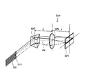
本実施形態は、いわゆる透過型の波長選択スイッチ500である。波長選択スイッチ500は、複数の光ファイバからなるファイバアレイ501と、マイクロレンズアレイ502と、グレーティング503と、レンズ504と、MEMSモジュールであるMEMSミラーアレイ505とを備えている。
(First embodiment)
Next, a wavelength selective switch according to a first embodiment of the present invention will be described with reference to FIG.
This embodiment is a so-called transmission-type wavelength
ファイバアレイ501内の各光ファイバとマイクロレンズアレイ502内の各マイクロレンズは対になっている。この対がアレイ状に配置されている。ファイバアレイ501は光入出力ポートとして機能する。その光ファイバのひとつ(以下、「第1の光ファイバ」という。)から、波長多重された信号光が、グレーティング503に向けて出射される。光ファイバから射出した光は、マイクロレンズアレイ502で平行光束に変換される。
Each optical fiber in the
グレーティング503として、上述した分散素子を用いる。マイクロレンズアレイから出射した光は、グレーティング503に入射する。グレーティング503は、波長多重光を帯状に分散する。
As the grating 503, the above-described dispersion element is used. The light emitted from the microlens array enters the
レンズ504はグレーティング503によって分散された光を、偏向部材であるMEMSミラーアレイ505上の波長ごとの所定位置に導く。
The
ここで、グレーティング503は、例えば、頂角34度のシリコンプリズムに反射型グレーティングGが形成されている、いわゆるイマージョン・グレーティングである。回折面はシリコンで満たされおり、1mmあたり2500本の溝が形成されている。
Here, the
MEMSモジュールであるMEMSミラーアレイ505は、グレーティング504で帯状に分散された光の波長に対応する複数のマイクロミラーMのアレイ(MEMSミラーアレイ)を有する。
The
マイクロミラーMは、図7を用いて説明したように、それぞれのミラーがローカルのx軸とy軸の周りに回転が可能で、主にy軸に関する回転により、入射した光を入射方向とは異なる方向へ反射する。 As described with reference to FIG. 7, the micromirror M can rotate around the local x-axis and y-axis, and the incident direction of the incident light is mainly due to rotation about the y-axis. Reflects in different directions.
各ミラーアレイにより、入射方向とおよそ同じ方向に反射された光は、レンズに504よりグレーティング503上に統合され、回折後は再び多波長成分の同一光束となる。
The light reflected by each mirror array in approximately the same direction as the incident direction is integrated on the grating 503 by the
これに対して、各ミラーアレイにより、入射方向と異なる方向に反射された光は、レンズ504によりグレーティング503上にリレーされるが、統合はされずそれぞれが回折される。そして、ファイバアレイ501のいずれかのファイバに入射する。
On the other hand, light reflected by each mirror array in a direction different from the incident direction is relayed onto the grating 503 by the
このように、第1の光ファイバから出射した多波長成分の光は、波長ごとにマイクロミラーアレイのそれぞれのミラーMの傾き角により選択的に他のファイバに入射させることができる。 As described above, the light of the multi-wavelength component emitted from the first optical fiber can be selectively made incident on another fiber depending on the inclination angle of each mirror M of the micromirror array for each wavelength.
なお、この実施例ではひとつの光入力ポートから複数の光出力ポートへの結合に関して説明したが、複数の光入力ポートからひとつの光出力ポートへの結合を行うことも可能である。 In this embodiment, the coupling from one optical input port to a plurality of optical output ports has been described. However, coupling from a plurality of optical input ports to one optical output port can also be performed.
本実施形態において、ファイバアレイ501は、光が出射する出射部、
グレーティング504は、ファイバアレイ501の光出射側に配置された分散素子、
MEMSミラーアレイ505は、グレーティング504の光出射側に配置された光偏向部材、
ファイバアレイ501は、MEMSミラーアレイ505からの光が入射する入射部、
マイクロレンズアレイ502は、ファイバアレイ501とMEMSミラーアレイ505と間の光路中に設けられている第1の光学系、
レンズ504は、グレーティング504とMEMSミラーアレイ505との光路中に設けられている第2の光学系である。
さらに、本実施形態では、
グレーティング504はレンズ504の前側焦点位置に設けられ、
MEMSミラーアレイ505はレンズ504の後側焦点位置に設けられている。
本実施形態では、従来の回折格子(プリズムなし)に代えて、本実施形態の分散素子を用いている。そのため、光学系を小型化できる。
In the present embodiment, the
The grating 504 is a dispersive element disposed on the light exit side of the
The
The
The
The
Furthermore, in this embodiment,
The grating 504 is provided at the front focal position of the
The
In this embodiment, the dispersive element of this embodiment is used instead of the conventional diffraction grating (no prism). Therefore, the optical system can be reduced in size.
(第2実施形態)
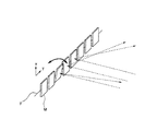
次に、図2を参照に本発明の第2実施形態に係る波長選択スイッチについて説明する。上記第1実施例と同一の部材には同一の符号を付す。
本実施形態は、いわゆる反射型の波長選択スイッチ600である。波長選択スイッチ600は、複数の光ファイバからなるファイバアレイ501と、マクロレンズアレイ502と、グレーティング503と、反射光学部材601と、MEMSモジュールであるMEMSミラーアレイ505とを備えている。
(Second Embodiment)
Next, a wavelength selective switch according to a second embodiment of the present invention will be described with reference to FIG. The same members as those in the first embodiment are denoted by the same reference numerals.
The present embodiment is a so-called reflection type wavelength
ファイバアレイ501内の各光ファイバとマイクロレンズアレイ502内の各マイクロレンズは、1対1に対応する対になっている。この対がアレイ状に配置されている。ファイバアレイ501は光入出力ポートとして機能する。その光ファイバのひとつ(以下、「第1の光ファイバ」という。)から、波長多重された信号光が、グレーティング503に向けて出射される。光ファイバから射出した光は、マイクロレンズアレイ502で平行光束に変換される。
Each optical fiber in the
グレーティング503として、上述した分散素子を用いる。マイクロレンズアレイ502から出射した光は、グレーティング503に入射する。グレーティング503は、波長多重光を帯状に分散する。
As the grating 503, the above-described dispersion element is used. Light emitted from the
反射光学部材601はグレーティング503によって分散された光を、偏向部材であるMEMSミラーアレイ505上の波長ごとの所定位置に導く。反射光学部材601は、例えば、凹面鏡を用いることができる。
The reflective optical member 601 guides the light dispersed by the grating 503 to a predetermined position for each wavelength on the
ここで、グレーティング503は、例えば、頂角34度のシリコンプリズムに反射型グレーティングGが形成されている、いわゆるイマージョングレーティングである。回折面はシリコンで満たされおり、1mmあたり2500本の溝が形成されている。
Here, the
MEMSモジュールであるMEMSミラーアレイ505は、グレーティング504とで帯状に分散された光の波長に対応するマイクロミラーMのアレイ(MEMSミラーアレイ)を有する。
The
マイクロミラーMは、図7を用いて説明したように、それぞれのミラーがローカルのx軸とy軸の周りに回転が可能で、主にy軸に関する回転により、入射した光を入射方向とは異なる方向へ反射する。 As described with reference to FIG. 7, the micromirror M can rotate around the local x-axis and y-axis, and the incident direction of the incident light is mainly due to rotation about the y-axis. Reflects in different directions.
各ミラーアレイにより、入射方向とおよそ同じ方向に反射された光は、反射光学部材601よりグレーティング503上に統合され、回折後は再び多波長成分の同一光束となる。 The light reflected by each mirror array in approximately the same direction as the incident direction is integrated on the grating 503 by the reflective optical member 601 and becomes the same light flux of multiple wavelength components again after diffraction.
これに対して、各ミラーアレイにより、入射方向と異なる方向に反射された光は、反射光学部材601によりグレーティング503上にリレーされるが、統合されずそれぞれが回折される。そして、ファイバアレイ501のいずれかのファイバに入射する。
In contrast, light reflected by each mirror array in a direction different from the incident direction is relayed on the grating 503 by the reflective optical member 601, but is not integrated and is diffracted. Then, the light enters one of the fibers in the
このように、第1の光ファイバから出射した多波長成分の光に関して、波長ごとにマイクロミラーアレイのそれぞれのミラーMの傾き角により選択的に他のファイバに入射させることができる。
なお、この実施例ではひとつの光入力ポートから複数の光出力ポートへの結合に関して説明したが、複数の光入力ポートからひとつの光出力ポートへの結合を行うことも可能である。
As described above, the light of the multi-wavelength component emitted from the first optical fiber can be selectively made incident on another fiber depending on the inclination angle of each mirror M of the micromirror array for each wavelength.
In this embodiment, the coupling from one optical input port to a plurality of optical output ports has been described. However, coupling from a plurality of optical input ports to one optical output port can also be performed.
本実施形態において、ファイバアレイ501は、光が出射する出射部、
グレーティング504は、ファイバアレイ501の光出射側に配置された分散素子、
MEMSミラーアレイ505は、グレーティング504の光出射側に配置された光偏向部材、
ファイバアレイ501は、MEMSミラーアレイ505からの光が入射する入射部、
マイクロレンズアレイ502は、ファイバアレイ501とMEMSミラーアレイ505との間の光路中に設けられている第1の光学系、
反射光学部材601は、グレーティング504とMEMSミラーアレイ505との光路中に設けられている第2の光学系である。
さらに、本実施形態では、
グレーティング504は反射光学部材601の前側焦点位置に設けられ、
MEMSミラーアレイ505は反射光学部材601の後側焦点位置に設けられている。
そのため、光学系を小型化できる。また、透過型の波長選択スイッチに比較して、さらに光学系を小型化できる。
In the present embodiment, the
The grating 504 is a dispersive element disposed on the light exit side of the
The
The
The
The reflective optical member 601 is a second optical system provided in the optical path between the grating 504 and the
Furthermore, in this embodiment,
The grating 504 is provided at the front focal position of the reflective optical member 601.
The
Therefore, the optical system can be reduced in size. Further, the optical system can be further downsized as compared with the transmission type wavelength selective switch.
以上のように、本発明にかかる波長選択スイッチは、高い波長分解能で分光し、小型化する場合に有用である。 As described above, the wavelength selective switch according to the present invention is useful in the case of performing spectroscopy with high wavelength resolution and downsizing.
200 分散素子
201a 入射面
201b 射出面
201c 回折光学面
220 プリズム
230 平面部材
300 分散素子
400 分散素子
500 波長選択スイッチ
501 ファイバアレイ
502 マイクロレンズアレイ
503 グレーティング
504 レンズ
505 MEMSミラーアレイ
600 波長選択スイッチ
601 反射光学部材
M マイクロミラー
G 回折格子
DESCRIPTION OF
Claims (8)
該出射部の光出射側に配置された分散素子と、
前記分散素子の光出射側に配置された光偏向部材と、
ファイバの端面で構成されている、前記光偏向部材からの光が入射する入射部と、
前記出射部と前記光偏向部材との間の光路中に設けられている第1の光学系と、
前記分散素子と前記光偏向部材との光路中に設けられている第2の光学系とを有し、
前記分散素子は前記第2の光学系の前側焦点位置に設けられ、
前記光偏向部材は前記第2の光学系の後側焦点位置に設けられ、
前記光偏向部材は複数の偏向素子で構成され、
該複数の偏向素子は、互いに独立して制御可能であり、
前記分散素子は、光が透過する透過面と、
回折光学面を有し、
前記透過面から前記回折光学面までの間が、屈折率が1よりも大きい媒質で形成されていることを特徴とする波長選択スイッチ。 An emission part configured by an end face of the fiber and emitting light;
A dispersive element disposed on the light exit side of the exit portion;
A light deflection member disposed on the light exit side of the dispersion element;
An incident part configured by an end face of a fiber and receiving light from the light deflection member;
A first optical system provided in an optical path between the emitting portion and the light deflection member;
A second optical system provided in an optical path between the dispersion element and the light deflection member;
The dispersive element is provided at a front focal position of the second optical system;
The light deflection member is provided at a rear focal position of the second optical system;
The light deflection member is composed of a plurality of deflection elements,
The plurality of deflection elements can be controlled independently of each other,
The dispersion element includes a transmission surface through which light is transmitted;
Having a diffractive optical surface,
A wavelength selective switch characterized in that a space between the transmission surface and the diffractive optical surface is formed of a medium having a refractive index larger than 1.
前記透過面は前記光が入射する入射面であり、
前記別の透過面は前記光が出射する出射面であり、
前記回折光学面は、前記入射面から前記出射面に到る光路中に配置され、
前記回折光学面は反射面であることを特徴とする請求項1に記載の波長選択スイッチ。 A transmission surface different from the transmission surface,
The transmission surface is an incident surface on which the light is incident,
The another transmission surface is an emission surface from which the light is emitted,
The diffractive optical surface is disposed in an optical path from the incident surface to the exit surface,
The wavelength selective switch according to claim 1, wherein the diffractive optical surface is a reflective surface.
前記入射面、前記出射面及び前記回折光学面は、1つの前記媒質に一体に形成されていることを特徴とする請求項1に記載の波長選択スイッチ。 The dispersive element comprises one medium;
2. The wavelength selective switch according to claim 1, wherein the entrance surface, the exit surface, and the diffractive optical surface are integrally formed on one medium.
前記入射面と前記出射面は前記第1の媒質に形成され、
前記回折光学面は、前記第2の媒質に形成されていることを特徴とする請求項2に記載の波長選択スイッチ。 The dispersion element includes a first medium and a second medium as the medium,
The entrance surface and the exit surface are formed in the first medium,
The wavelength selective switch according to claim 2, wherein the diffractive optical surface is formed in the second medium.
The wavelength selective switch according to any one of claims 1 to 5, wherein the second optical system is a concave mirror.
Priority Applications (1)
| Application Number | Priority Date | Filing Date | Title |
|---|---|---|---|
| JP2008307487A JP2010134027A (en) | 2008-12-02 | 2008-12-02 | Wavelength selection switch |
Applications Claiming Priority (1)
| Application Number | Priority Date | Filing Date | Title |
|---|---|---|---|
| JP2008307487A JP2010134027A (en) | 2008-12-02 | 2008-12-02 | Wavelength selection switch |
Publications (2)
| Publication Number | Publication Date |
|---|---|
| JP2010134027A true JP2010134027A (en) | 2010-06-17 |
| JP2010134027A5 JP2010134027A5 (en) | 2012-01-19 |
Family
ID=42345399
Family Applications (1)
| Application Number | Title | Priority Date | Filing Date |
|---|---|---|---|
| JP2008307487A Pending JP2010134027A (en) | 2008-12-02 | 2008-12-02 | Wavelength selection switch |
Country Status (1)
| Country | Link |
|---|---|
| JP (1) | JP2010134027A (en) |
Cited By (3)
| Publication number | Priority date | Publication date | Assignee | Title |
|---|---|---|---|---|
| CN102129125A (en) * | 2011-01-10 | 2011-07-20 | 中国科学院上海微系统与信息技术研究所 | Stacked dual-shaft micro lens array driver based on MEMS (Micro Electronic Mechanical System) technology and use thereof |
| US8634129B2 (en) | 2011-02-10 | 2014-01-21 | Olympus Corporation | Wavelength selective switch |
| CN103792622A (en) * | 2014-01-14 | 2014-05-14 | 武汉邮电科学研究院 | Programmable WSS based on MEMS micro-mirror array and deformable mirror and implementation method |
Citations (4)
| Publication number | Priority date | Publication date | Assignee | Title |
|---|---|---|---|---|
| JP2003509714A (en) * | 1999-09-14 | 2003-03-11 | コーニング・インコーポレーテッド | Thermal and high throughput gratings |
| JP2003075622A (en) * | 2001-09-05 | 2003-03-12 | Toshiba Corp | Diffraction grating, method for processing diffraction grating and optical element |
| JP2004532544A (en) * | 2001-03-19 | 2004-10-21 | カペラ フォトニクス インコーポレイテッド | Reconfigurable optical add / drop multiplexer |
| US20050276537A1 (en) * | 2004-06-14 | 2005-12-15 | Engana Pty Ltd | Dual-source optical wavelength processor |
-
2008
- 2008-12-02 JP JP2008307487A patent/JP2010134027A/en active Pending
Patent Citations (4)
| Publication number | Priority date | Publication date | Assignee | Title |
|---|---|---|---|---|
| JP2003509714A (en) * | 1999-09-14 | 2003-03-11 | コーニング・インコーポレーテッド | Thermal and high throughput gratings |
| JP2004532544A (en) * | 2001-03-19 | 2004-10-21 | カペラ フォトニクス インコーポレイテッド | Reconfigurable optical add / drop multiplexer |
| JP2003075622A (en) * | 2001-09-05 | 2003-03-12 | Toshiba Corp | Diffraction grating, method for processing diffraction grating and optical element |
| US20050276537A1 (en) * | 2004-06-14 | 2005-12-15 | Engana Pty Ltd | Dual-source optical wavelength processor |
Cited By (4)
| Publication number | Priority date | Publication date | Assignee | Title |
|---|---|---|---|---|
| CN102129125A (en) * | 2011-01-10 | 2011-07-20 | 中国科学院上海微系统与信息技术研究所 | Stacked dual-shaft micro lens array driver based on MEMS (Micro Electronic Mechanical System) technology and use thereof |
| CN102129125B (en) * | 2011-01-10 | 2017-02-08 | 中国科学院上海微系统与信息技术研究所 | Stacked dual-shaft micro lens array driver based on MEMS (Micro Electronic Mechanical System) technology and use thereof |
| US8634129B2 (en) | 2011-02-10 | 2014-01-21 | Olympus Corporation | Wavelength selective switch |
| CN103792622A (en) * | 2014-01-14 | 2014-05-14 | 武汉邮电科学研究院 | Programmable WSS based on MEMS micro-mirror array and deformable mirror and implementation method |
Similar Documents
| Publication | Publication Date | Title |
|---|---|---|
| US6956687B2 (en) | Optical blocking filter having an array of micro-mirrors | |
| US7126740B2 (en) | Multifunctional optical device having a spatial light modulator with an array of micromirrors | |
| JP5184637B2 (en) | Wavelength selective switch | |
| JP2006276216A (en) | Optical switch | |
| US8125639B2 (en) | Temperature compensated spectroscope and optical apparatus | |
| WO2012172968A1 (en) | Optical device | |
| WO1999046628A1 (en) | Optical demultiplexer and method of assembling the same | |
| US6922277B2 (en) | Optical interleaver/deinterleaver device having an array of micro-mirrors | |
| JP6172928B2 (en) | Optical processing device using a digital micromirror device (DMD) with reduced wavelength dependent loss | |
| US20030095307A1 (en) | Reconfigurable optical add/drop multiplexer having an array of micro-mirrors | |
| US20030090756A1 (en) | Optical channel monitor having an array of micro-mirrors | |
| JP4967847B2 (en) | Optical switch and MEMS package | |
| US8531769B2 (en) | Dispersion element, spectral device, and wavelength selective switch | |
| JP2010134027A (en) | Wavelength selection switch | |
| JP2000299521A (en) | Single dimension self-aligned retroreflecting optical system for wavelength filtering | |
| JP2010128473A (en) | Dispersion element and optical equipment with dispersion element | |
| JP2010128473A5 (en) | ||
| JP2004271743A (en) | Optical device | |
| JP4407382B2 (en) | Optical filter device | |
| JP2010134027A5 (en) | ||
| JP2006039304A (en) | Optical switch | |
| EP2570829B1 (en) | Optical processing device | |
| JP4192767B2 (en) | Optical signal processor manufacturing method | |
| JP5508368B2 (en) | Wavelength selective switch | |
| JP2012203136A (en) | Wavelength selecting switch |
Legal Events
| Date | Code | Title | Description |
|---|---|---|---|
| A521 | Written amendment |
Effective date: 20111125 Free format text: JAPANESE INTERMEDIATE CODE: A523 |
|
| A621 | Written request for application examination |
Free format text: JAPANESE INTERMEDIATE CODE: A621 Effective date: 20111125 |
|
| A977 | Report on retrieval |
Effective date: 20120913 Free format text: JAPANESE INTERMEDIATE CODE: A971007 |
|
| A131 | Notification of reasons for refusal |
Effective date: 20120926 Free format text: JAPANESE INTERMEDIATE CODE: A131 |
|
| A02 | Decision of refusal |
Free format text: JAPANESE INTERMEDIATE CODE: A02 Effective date: 20130206 |