JP6172928B2 - Optical processing device using a digital micromirror device (DMD) with reduced wavelength dependent loss - Google Patents
Optical processing device using a digital micromirror device (DMD) with reduced wavelength dependent loss Download PDFInfo
- Publication number
- JP6172928B2 JP6172928B2 JP2012272107A JP2012272107A JP6172928B2 JP 6172928 B2 JP6172928 B2 JP 6172928B2 JP 2012272107 A JP2012272107 A JP 2012272107A JP 2012272107 A JP2012272107 A JP 2012272107A JP 6172928 B2 JP6172928 B2 JP 6172928B2
- Authority
- JP
- Japan
- Prior art keywords
- optical
- optical element
- wavelength
- collimating
- compensating
- Prior art date
- Legal status (The legal status is an assumption and is not a legal conclusion. Google has not performed a legal analysis and makes no representation as to the accuracy of the status listed.)
- Active
Links
- 230000003287 optical effect Effects 0.000 title claims description 144
- 238000012545 processing Methods 0.000 title claims description 30
- 230000001419 dependent effect Effects 0.000 title claims description 22
- 239000000835 fiber Substances 0.000 claims description 51
- 230000008878 coupling Effects 0.000 claims description 28
- 238000010168 coupling process Methods 0.000 claims description 28
- 238000005859 coupling reaction Methods 0.000 claims description 28
- 238000000034 method Methods 0.000 claims description 5
- 230000003044 adaptive effect Effects 0.000 claims description 3
- 239000013307 optical fiber Substances 0.000 claims 4
- 238000003780 insertion Methods 0.000 description 3
- 230000037431 insertion Effects 0.000 description 3
- VYPSYNLAJGMNEJ-UHFFFAOYSA-N Silicium dioxide Chemical compound O=[Si]=O VYPSYNLAJGMNEJ-UHFFFAOYSA-N 0.000 description 2
- 230000000903 blocking effect Effects 0.000 description 2
- 238000000926 separation method Methods 0.000 description 2
- 238000013459 approach Methods 0.000 description 1
- 238000003491 array Methods 0.000 description 1
- 238000012937 correction Methods 0.000 description 1
- 238000010586 diagram Methods 0.000 description 1
- 238000005498 polishing Methods 0.000 description 1
- 239000000377 silicon dioxide Substances 0.000 description 1
- 239000012780 transparent material Substances 0.000 description 1
Images


Classifications
-
- G—PHYSICS
- G02—OPTICS
- G02B—OPTICAL ELEMENTS, SYSTEMS OR APPARATUS
- G02B5/00—Optical elements other than lenses
- G02B5/18—Diffraction gratings
-
- G—PHYSICS
- G02—OPTICS
- G02B—OPTICAL ELEMENTS, SYSTEMS OR APPARATUS
- G02B6/00—Light guides; Structural details of arrangements comprising light guides and other optical elements, e.g. couplings
- G02B6/24—Coupling light guides
- G02B6/26—Optical coupling means
- G02B6/28—Optical coupling means having data bus means, i.e. plural waveguides interconnected and providing an inherently bidirectional system by mixing and splitting signals
- G02B6/293—Optical coupling means having data bus means, i.e. plural waveguides interconnected and providing an inherently bidirectional system by mixing and splitting signals with wavelength selective means
- G02B6/29304—Optical coupling means having data bus means, i.e. plural waveguides interconnected and providing an inherently bidirectional system by mixing and splitting signals with wavelength selective means operating by diffraction, e.g. grating
- G02B6/29305—Optical coupling means having data bus means, i.e. plural waveguides interconnected and providing an inherently bidirectional system by mixing and splitting signals with wavelength selective means operating by diffraction, e.g. grating as bulk element, i.e. free space arrangement external to a light guide
- G02B6/29313—Optical coupling means having data bus means, i.e. plural waveguides interconnected and providing an inherently bidirectional system by mixing and splitting signals with wavelength selective means operating by diffraction, e.g. grating as bulk element, i.e. free space arrangement external to a light guide characterised by means for controlling the position or direction of light incident to or leaving the diffractive element, e.g. for varying the wavelength response
- G02B6/29314—Optical coupling means having data bus means, i.e. plural waveguides interconnected and providing an inherently bidirectional system by mixing and splitting signals with wavelength selective means operating by diffraction, e.g. grating as bulk element, i.e. free space arrangement external to a light guide characterised by means for controlling the position or direction of light incident to or leaving the diffractive element, e.g. for varying the wavelength response by moving or modifying the diffractive element, e.g. deforming
-
- G—PHYSICS
- G02—OPTICS
- G02B—OPTICAL ELEMENTS, SYSTEMS OR APPARATUS
- G02B5/00—Optical elements other than lenses
- G02B5/08—Mirrors
-
- G—PHYSICS
- G02—OPTICS
- G02B—OPTICAL ELEMENTS, SYSTEMS OR APPARATUS
- G02B6/00—Light guides; Structural details of arrangements comprising light guides and other optical elements, e.g. couplings
- G02B6/24—Coupling light guides
- G02B6/26—Optical coupling means
- G02B6/35—Optical coupling means having switching means
- G02B6/351—Optical coupling means having switching means involving stationary waveguides with moving interposed optical elements
- G02B6/3512—Optical coupling means having switching means involving stationary waveguides with moving interposed optical elements the optical element being reflective, e.g. mirror
- G02B6/3518—Optical coupling means having switching means involving stationary waveguides with moving interposed optical elements the optical element being reflective, e.g. mirror the reflective optical element being an intrinsic part of a MEMS device, i.e. fabricated together with the MEMS device
-
- G—PHYSICS
- G02—OPTICS
- G02B—OPTICAL ELEMENTS, SYSTEMS OR APPARATUS
- G02B6/00—Light guides; Structural details of arrangements comprising light guides and other optical elements, e.g. couplings
- G02B6/24—Coupling light guides
- G02B6/26—Optical coupling means
- G02B6/35—Optical coupling means having switching means
- G02B6/354—Switching arrangements, i.e. number of input/output ports and interconnection types
- G02B6/356—Switching arrangements, i.e. number of input/output ports and interconnection types in an optical cross-connect device, e.g. routing and switching aspects of interconnecting different paths propagating different wavelengths to (re)configure the various input and output links
-
- G—PHYSICS
- G02—OPTICS
- G02B—OPTICAL ELEMENTS, SYSTEMS OR APPARATUS
- G02B6/00—Light guides; Structural details of arrangements comprising light guides and other optical elements, e.g. couplings
- G02B6/24—Coupling light guides
- G02B6/26—Optical coupling means
- G02B6/35—Optical coupling means having switching means
- G02B6/351—Optical coupling means having switching means involving stationary waveguides with moving interposed optical elements
- G02B6/3512—Optical coupling means having switching means involving stationary waveguides with moving interposed optical elements the optical element being reflective, e.g. mirror
- G02B6/3516—Optical coupling means having switching means involving stationary waveguides with moving interposed optical elements the optical element being reflective, e.g. mirror the reflective optical element moving along the beam path, e.g. controllable diffractive effects using multiple micromirrors within the beam
Description
本発明は光学処理デバイスに関する。 The present invention relates to an optical processing device.
従来は、光ビームを分散させるための分散素子(例えば、回折格子)および分散したビームのそれぞれでの各波長が複数の出力経路のいずれかに入射することを可能にする作動可能光学素子を含む光学処理デバイスが使用されてきた。 Conventionally, includes a dispersive element (eg, a diffraction grating) for dispersing a light beam and an operable optical element that allows each wavelength in each of the dispersed beams to enter one of a plurality of output paths Optical processing devices have been used.
そのような作動可能光学素子の一例は、DMD(デジタルマイクロミラーデバイス)であり、DMDは、それぞれが個々に作動可能なマイクロミラー素子のアレイを含む。DMDは、ミラー素子の位置を調整して波長成分が反射される方向を制御することによって、反射された波長成分の光路を複数出力経路のいずれか1つに選択的に切り替えることができる。そのような光学処理デバイスは、切替え、波長減衰および波長遮断を含む様々な異なる目的のために様々な異なる方法で光ビームでの波長を処理するために使用できる。 One example of such an actuable optical element is a DMD (Digital Micromirror Device), which includes an array of micromirror elements that are individually actuable. The DMD can selectively switch the optical path of the reflected wavelength component to any one of a plurality of output paths by adjusting the position of the mirror element to control the direction in which the wavelength component is reflected. Such optical processing devices can be used to process wavelengths in a light beam in a variety of different ways for a variety of different purposes including switching, wavelength attenuation and wavelength blocking.
本発明の課題は、作動可能光学素子および補償光学素子を含む光学装置を提供することである。 It is an object of the present invention to provide an optical device that includes an operable optical element and an adaptive optical element.
本発明の一態様によると、作動可能光学素子および補償光学素子を含む光学装置が、提供される。作動可能光学素子は、複数の空間的に分離された波長成分を有する光ビームを受け取り、その複数の波長成分を波長に依存する仕方で回折するために設けられる。補償光学素子は、光ビームを作動可能光学素子に導く。補償光学素子は、波長成分が作動可能光学素子によって回折される波長に依存する仕方を補償する。 According to one aspect of the invention, an optical device is provided that includes an actuable optical element and an adaptive optical element. An actuable optical element is provided for receiving a light beam having a plurality of spatially separated wavelength components and diffracting the plurality of wavelength components in a wavelength dependent manner. The compensating optical element directs the light beam to the operable optical element. The compensating optical element compensates for the manner in which the wavelength component depends on the wavelength diffracted by the operable optical element.
本発明の別の態様によると、光学処理デバイスは、光ビームを受け取るための少なくとも2つの光入力/出力ポートと、ポートの1つから光ビームを受け取り、その光ビームを複数の波長成分に空間的に分離するための分散素子とを含む。本デバイスはまた、複数の波長成分をコリメートするためのコリメート用レンズおよび作動可能光学素子も含む。作動可能光学素子は、コリメート用素子からコリメートされた波長成分を受け取り、複数の波長成分を波長に依存する仕方で回折するために設けられる。補償光学素子は、分散素子と作動可能光学素子との間の光路に置かれる。補償光学素子は、波長成分が作動可能光学素子によって回折される波長に依存する仕方を補償する。 According to another aspect of the invention, an optical processing device receives at least two light input / output ports for receiving a light beam and a light beam from one of the ports and spatially separates the light beam into a plurality of wavelength components. And a dispersive element for separation. The device also includes a collimating lens and an operable optical element for collimating a plurality of wavelength components. The actuatable optical element is provided for receiving the collimated wavelength component from the collimating element and diffracting the plurality of wavelength components in a wavelength dependent manner. The compensating optical element is placed in the optical path between the dispersive element and the operable optical element. The compensating optical element compensates for the manner in which the wavelength component depends on the wavelength diffracted by the operable optical element.
多くの光学処理デバイスは、入射光ビームおよび出射光ビームを同じ光路に沿って導く。そのようなデバイスとしては、光スイッチ、ウェーブブロッカー(waveblocker)および光減衰器が挙げられる。図1は、DMDなどのMEMSミラーアレイに基づく波長ブロッカーの簡単な例を示す。1×1波長ブロッカーでは、ファイバーアレイは、入力ポートおよび出力ポートとしての役割を果たす単一ファイバーである。しばしばサーキュレータ(図示せず)または他の手段が、入射ビームおよび出射ビームを分離するために使用される。もしファイバーアレイが、N本のファイバーを含むならば、各ファイバーは、入力ポートおよび出力ポートとしての役割を果たす。そのようなデバイスは、共通の光学的組織を使用するN個の1×1波長ブロッカーを備え、波長ブロッカーアレイと呼ばれる。そのようなデバイスでは、ローンチ光学系は一般に、N本の入射ビームおよびN本の出射ビームのそれぞれを分離するためにファイバーアレイおよび一連のサーキュレータまたは同様のものを必要とすることになる。
Many optical processing devices direct incident and outgoing light beams along the same optical path. Such devices include optical switches, waveblockers and optical attenuators. FIG. 1 shows a simple example of a wavelength blocker based on a MEMS mirror array such as DMD. In a 1 × 1 wavelength blocker, the fiber array is a single fiber that serves as an input port and an output port. Often circulators (not shown) or other means are used to separate the incoming and outgoing beams. If the fiber array contains N fibers, each fiber serves as an input port and an output port. Such a device comprises
光学処理デバイスの別の例は、図2で示される。この特定の例では、N(例えば、15)個の1×1スイッチが、結合ミラーを使用して形成される。この例では、より簡単で、より安価なローンチ光学系装置が用いられ、それはサーキュレータまたは同様のものが必要となるのを避ける。ローンチ光学系装置260は、小型レンズアレイ200との組合せたファイバーアレイ250を含む。ファイバーアレイ250は典型的には、入力/出力ファイバーを固定する2つのV溝プレートから成る。図2は、2つのファイバー対を示し、対1は、ファイバー1および2を含み、対2は、ファイバー3および4を含む。
Another example of an optical processing device is shown in FIG. In this particular example, N (eg, 15) 1 × 1 switches are formed using coupled mirrors. In this example, a simpler and less expensive launch optics device is used, which avoids the need for a circulator or the like. The launch
例示するために、図2で示すローンチ光学系装置260の例は、ファイバーアレイを含むが、より一般にローンチ光学系装置260は、例えば平面導波路アレイなどの任意の種類の導波路アレイを含んでもよいことに留意すべきである。その上、アレイで用いられる導波路は、すべて同じ種類または異なる種類(例えば、ファイバーおよび平面導波路)の組合せであってもよい。
To illustrate, the example
小型レンズアレイ200は、内側および外側の対向する表面220および230を含み、シリカまたは別の光学的に透明な適切な材料から形成される。一連のコリメート用レンズ対2101、2102、2103・・・は、小型レンズアレイ200の内側表面220に配置される。各コリメート用レンズ対210は、2つのコリメート用レンズ212を含む。同様に、一連の結合レンズ2141、2142、2143・・・は、小型レンズアレイ200の外側表面230に形成される。各コリメート用レンズ対210は、結合レンズ214の1つと位置合わせされている。例えば、図2では、コリメート用レンズ対2101は、結合レンズ2141と位置合わせされており、コリメート用レンズ対2102は、結合レンズ2142と位置合わせされている。それ故に、結合レンズ214の2倍の数のコリメート用レンズ212がある。
The
コリメート用レンズ212のピッチは、ファイバーアレイ250でのファイバーのピッチと同じである。それに応じて、ファイバーアレイ250および小型レンズアレイ200は、小型レンズアレイ200のコリメート用レンズ212のそれぞれが、ファイバーアレイ250でのファイバー出力の1つと位置合わせされるように配置される。いくつかの特定の実装形態では、コリメート用レンズ212と結合レンズ214との間の分離は、それらの個々の焦点距離の和にほぼ等しくてもよい。
The pitch of the
図2でのローンチ光学系装置260の動作は、次の通りである。各ファイバー対の入力ファイバーからの光ビームは、ファイバーアレイ250から小型レンズアレイ200に、小型レンズアレイ200が位置合わせされているコリメート用レンズ212を通って伝えられる。例えば、図2では、ファイバー1からの光は、コリメート用レンズ対2101の対応するコリメート用レンズ212に入ることが示される。コリメート用レンズ212は、コリメートされたビームをコリメート用レンズ212が位置合わせされている結合レンズ214に導く。図2では、ファイバー1からのコリメートされるビームは、コリメート用レンズ対2101のコリメート用レンズ212によってコリメートされ、そのコリメート用レンズ212は、コリメートされたビームを結合レンズ2141に導く。
The operation of the launch
結合レンズ214は次に、ビームをローンチ平面に合焦し、その平面には、図2で示す例では、結合ミラー240が置かれている。結合ミラー240は、ビームを受け取った同じ結合レンズ(例えば、図2での結合レンズ2141)を通ってビームが戻るようにビームを反射する。結合レンズ214は、反射されたビームをコリメートし、小型レンズアレイ200を通って戻るようにビームを導く。ビームが結合ミラー240によって反射された角度のために、コリメートされた反射ビームは、コリメートされた入射ビームに平行であり、コリメートされた入射ビームから空間的にオフセットされている。コリメートされた反射ビームは、最初にビームをファイバーアレイ250から受け取ったコリメート用レンズ対の出力コリメート用レンズに導かれる。図2で示すように、例えば、コリメート用レンズ対2101の入力コリメート用レンズ212を通って小型レンズアレイ200に導かれたビームは、コリメート用レンズ対2101の隣接する出力コリメート用レンズ212に導かれる。出力コリメート用レンズ212は、反射ビームを出力コリメート用レンズ212と位置合わせされているファイバーの入力に合焦し、そのファイバーは、図2で示す例では、ファイバー2である。このようにして、図2で示す光学処理デバイスは、ファイバー対の1つのファイバー(例えば、ファイバー1)から受け取った入力ビームを同じファイバー対の別のファイバー(例えば、ファイバー2)に導き、それ故に切替え機能を提供する。
The coupling lens 214 then focuses the beam on the launch plane, in which the
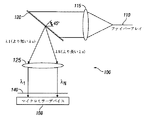
光学処理デバイスの別の例は、図3a(側面図)および図3b(上面図)で示される。この例は、図2で示すのと同じ光学的ローンチ装置を用いているが、DMD550を含む光学システムで結合ミラー240を置き換える。この特定の例では、N個の1×1波長ブロッカーが形成される。もし例えば光学処理デバイスが、15個の1×1波長ブロッカー(そのうちの3個だけが図3で示される)を含むならば、ファイバーアレイ505は、30本の入力/出力ファイバーを含むことになる。
Another example of an optical processing device is shown in FIGS. 3a (side view) and 3b (top view). This example uses the same optical launch device as shown in FIG. 2, but replaces the
図示するように、光学的ローンチ装置570に続いて、コリメート用レンズ516、回折格子522、走査レンズ530、補償プリズム540およびDMD550がある。図3bの上面図で最もよくわかるように、DMD550は、ローンチ光学系装置570のファイバーが広がる平面で走査レンズ530の光学軸に関して傾斜している。
As shown, the optical launch device 570 is followed by a
動作中は、ファイバー502から光学的ローンチ装置570に入る光ビームは、対応する結合レンズ514から出て、ローンチ平面511での虚焦点に達する。光ビームは次いで、コリメート用レンズ516によってコリメートされる。回折格子522は次に、コリメートされたビームを回折し、走査レンズ530は、補償プリズム540を通過した後スペクトル的に分散したビームをDMD550に合焦する。通過状態に設定されるときは、DMD550の個々のミラーは、ビームをそれ自体のほとんど後ろに反射するように傾斜し(リトロー(Littrow)配置に近い)、その結果ビームは、デバイスを通って戻り、ローンチ光学系装置570の対応する導波路504を通って出る。別法として、遮断状態に設定されるときは、DMD550の個々のミラーは、ビームをデバイスから出させる角度に傾斜するように動かされる(図3bでのビーム560を参照)。図3は、結合したファイバー対502および504だけについての動作を示すが、上で述べた結合は、ファイバー対のすべてについて生じる。
In operation, the light beam entering the optical launch device 570 from the
DMD550が傾斜しているので、走査レンズ530からDMD550までの距離は、ファイバーによって異なる。補償プリズム540の機能は、すべてのファイバーからのビームをDMD550に合焦するようにこの経路長差を補正することである。補償プリズム540の動作は、補償プリズム540とDMD550との間の関係を示す図4でより容易に見ることができ、DMD550は、透明窓420を含んでもよい。
Since the
図3で示すデバイスは、その性能を制限する固有の波長依存損失を有する。この波長依存損失の原因を理解するため、DMD550は、微小ミラーのアレイで構成され、それ故にミラーよりもむしろ回折格子として振る舞うと考慮されたい。厳密に言えば、ビームは、DMDから回折され、反射されない。ファイバーアレイ505の平面でのDMD550からの回折角は、回折格子の式、
The device shown in FIG. 3 has an inherent wavelength dependent loss that limits its performance. To understand the cause of this wavelength dependent loss, consider that

によって与えられる。
ただしnは回折次数、dはDMDのピクセル間隔、また、λは波長である。従って、DMDからのビームの回折角は、波長依存である。結果として、入力ファイバーと出力ファイバーとの間の結合は、単一波長について最適化できるだけであり、それ故に光ビームは、デバイスを通って導かれるとき波長依存損失を経験する。
Given by.
Where n is the diffraction order, d is the pixel spacing of the DMD, and λ is the wavelength. Therefore, the diffraction angle of the beam from the DMD is wavelength dependent. As a result, the coupling between the input fiber and the output fiber can only be optimized for a single wavelength, and therefore the light beam experiences a wavelength dependent loss when guided through the device.
図5は、補償プリズム540を通過し、DMD550から回折するときの2つのビーム、短波長ビーム370および長波長ビーム380を示す。長波長ビーム380は、短波長ビーム370と比較してより大きな角度で回折する。波長と回折角との間のこの関係は、図6aおよび図6bを参照すると明らかになる。図6aは、短波長ビーム370(実線)がDMD550から回折されるところを示す。図6aはまた、ビーム370が回折される回折角θdも示す。図6bは同様に、長波長ビーム380(実線)がDMD550から回折される様子を示す。図6bはまた、ビーム380が回折される回折角θdも示す。図6aおよび図6bの比較は、より長い波長のビーム380がより大きな角度で回折することを示す。
FIG. 5 shows two beams as they pass through
波長依存損失は、適切な光学素子を設けてDMDからの回折によって導入される回折角の波長依存性を補償することによって最小化または除去できる。一般に、この光学素子は、図3での回折格子522から下流に、典型的にはDMD550の近くに置くべきである。すなわち、光学素子は、回折格子522とDMD550との間に置かれてもよい。一実装形態では、回折角の波長依存性を補償するために追加の光学素子を加える代わりに、既存の光学素子がこの機能を果たすように変更されてもよい。例えば、図3での補償プリズム540の形状が、この損失を補正するように変更されてもよい。この場合には、補償プリズム540は、各ファイバーからのビームが経験する経路長差の調整もし、DMD回折から生じる波長依存損失の補償もする。
The wavelength dependent loss can be minimized or eliminated by providing appropriate optical elements to compensate for the wavelength dependence of the diffraction angle introduced by diffraction from the DMD. In general, this optical element should be placed downstream from the
特定の一実装形態では、わずかなねじれが、補償プリズム540の表面の1つまたは両方に加えられてもよい。そのようなプリズムの一例は、補償プリズム385の入射表面394について図7で示される。図示されるように、表面394は、長波長ビーム392を短波長ビーム390よりも大きな屈折角で屈折させる。この例では、表面394は、z=mxy(ゼルニケ多項式の第5項)の形を有し、それは、2つの交差円柱の和と考えることができる。そのような表面の形状が、図8で示される。結果として、波長依存損失の補正はまた、補償プリズム385の各表面に円柱面を加えることによっても達成できる。この手法の1つの利点は、円柱面が従来の光学研磨方法を使用して生成できることである。
In one particular implementation, a slight twist may be applied to one or both of the surfaces of the
再び図4を参照すると、いくつかの実装形態では、DMD550、窓420および補償プリズム540(または他の適切な補償光学素子)を単一ユニットにまとめ、光ビームを波長に依存しない仕方で回折するDMD装置を実現することができる。そのようなDMD装置は、多種多様な異なる光学処理デバイスで使用できる。
Referring again to FIG. 4, in some implementations,
図9aおよび図9bは、DMDからの回折角への波長依存性の補償がない場合および回折角への波長依存性の補償がある場合の例示的な光学処理デバイスについて、Cバンドの一部にわたる挿入損失をそれぞれ示す。図示するように、波長依存性が低減されると、損失の量および損失の変動が低減される。 FIGS. 9a and 9b illustrate a portion of the C-band for an exemplary optical processing device without wavelength dependent compensation to diffraction angle from DMD and with wavelength dependent compensation to diffraction angle. The insertion loss is shown respectively. As shown, when the wavelength dependence is reduced, the amount of loss and fluctuations in loss are reduced.
200 小型レンズアレイ
210 コリメート用レンズ対
212 コリメート用レンズ
214 結合レンズ
220 内側表面
230 外側表面
240 結合ミラー
250 ファイバーアレイ
260 ローンチ光学系装置
370 短波長ビーム
380 長波長ビーム
385 補償プリズム
390 短波長ビーム
392 長波長ビーム
394 補償プリズムの入射表面
420 透明窓
502 ファイバー
504 導波路、ファイバー
505 ファイバーアレイ
511 ローンチ平面
514 結合レンズ
516 コリメート用レンズ
522 回折格子
530 走査レンズ
540 補償プリズム
550 DMD
560 ビーム
570 光学的ローンチ装置、ローンチ光学系装置
200 small lens array 210
560 beam 570 optical launch device, launch optical system device
Claims (23)
前記光ビームを前記作動可能光学素子に導く補償光学素子であって、前記波長成分が前記作動可能光学素子によって回折される前記それぞれの波長に依存する仕方によって引き起こされる、回折される波長成分の光結合損失を低減する補償光学素子と、
を備えることを特徴とする光学配置。 An actuable optical element for receiving a light beam having a plurality of spatially separated wavelength components and diffracting the plurality of wavelength components in a manner dependent on the respective wavelengths;
Compensating optical element for directing the light beam to the actuatable optical element, the light of the diffracted wavelength component caused by the wavelength component being dependent on the respective wavelength diffracted by the actuatable optical element An adaptive optics element that reduces coupling losses ;
An optical arrangement comprising:
前記光ビームを前記光入力/出力ポートの1つから受け取り、前記光ビームを複数の波長成分に空間的に分離する分散素子と、
前記複数の波長成分をコリメートするためのコリメート用レンズと、
前記コリメートされた波長成分を前記コリメート用レンズから受け取り、前記複数の波長成分をそれぞれの波長に依存する仕方で回折するための作動可能光学素子と、
前記分散素子と前記作動可能光学素子との間の光路に置かれる補償光学素子であって、前記波長成分が前記作動可能光学素子によって回折される前記それぞれ波長に依存する仕方によって引き起こされる回折される波長成分の光結合損失を前記補償光学素子が低減する補償光学素子と、
を含むことを特徴とする光学処理デバイス。 At least two optical input / output ports for receiving a light beam;
A dispersive element that receives the light beam from one of the light input / output ports and spatially separates the light beam into a plurality of wavelength components;
A collimating lens for collimating the plurality of wavelength components;
An actuable optical element for receiving the collimated wavelength component from the collimating lens and diffracting the plurality of wavelength components in a manner dependent on each wavelength;
A compensating optical element placed in the optical path between the dispersive element and the actuatable optical element, wherein the wavelength component is diffracted caused by the respective wavelength dependent manner diffracted by the actuatable optical element A compensation optical element that reduces the optical coupling loss of the wavelength component by the compensation optical element;
An optical processing device comprising:
前記波長成分が前記作動可能光学素子によって回折される前記それぞれ波長に依存する仕方によって引き起こされる回折される波長成分の光結合損失を補償光学素子が低減するステップと、
を含むことを特徴とする光信号を処理する方法。 Diffracting a plurality of spatially separated wavelength components using an operable optical element in a manner dependent on each wavelength;
A compensating optical element reducing optical coupling loss of the diffracted wavelength component caused by the respective wavelength dependent manner in which the wavelength component is diffracted by the actuatable optical element;
A method of processing an optical signal comprising:
前記コリメートされた波長成分がすべて共通の光路長を進むように回折される前に前記コリメートされた波長成分が経験する光路長を調整するステップと、
をさらに含むことを特徴とする請求項21に記載の方法。 Collimating the plurality of wavelength components;
Adjusting the optical path length experienced by the collimated wavelength components before being diffracted so that all the collimated wavelength components travel along a common optical path length;
The method of claim 21, further comprising:
Applications Claiming Priority (2)
| Application Number | Priority Date | Filing Date | Title |
|---|---|---|---|
| US13/325,555 | 2011-12-14 | ||
| US13/325,555 US8681422B2 (en) | 2011-12-14 | 2011-12-14 | Optical processing device employing a digital micromirror device (DMD) and having reduced wavelength dependent loss |
Publications (3)
| Publication Number | Publication Date |
|---|---|
| JP2013125278A JP2013125278A (en) | 2013-06-24 |
| JP2013125278A5 JP2013125278A5 (en) | 2015-12-24 |
| JP6172928B2 true JP6172928B2 (en) | 2017-08-02 |
Family
ID=47562918
Family Applications (1)
| Application Number | Title | Priority Date | Filing Date |
|---|---|---|---|
| JP2012272107A Active JP6172928B2 (en) | 2011-12-14 | 2012-12-13 | Optical processing device using a digital micromirror device (DMD) with reduced wavelength dependent loss |
Country Status (8)
| Country | Link |
|---|---|
| US (1) | US8681422B2 (en) |
| EP (1) | EP2605051B1 (en) |
| JP (1) | JP6172928B2 (en) |
| KR (1) | KR101958395B1 (en) |
| CN (1) | CN103163642B (en) |
| AU (1) | AU2012261755B2 (en) |
| BR (1) | BR102012032078A2 (en) |
| CA (1) | CA2798382A1 (en) |
Families Citing this family (7)
| Publication number | Priority date | Publication date | Assignee | Title |
|---|---|---|---|---|
| JP6322926B2 (en) * | 2013-08-12 | 2018-05-16 | 大日本印刷株式会社 | Illumination device, projection device, and projection display device |
| JP6251202B2 (en) * | 2015-01-27 | 2017-12-20 | 日本電信電話株式会社 | Wavelength selective switch |
| US10228517B2 (en) * | 2015-03-03 | 2019-03-12 | Nistica, Inc. | Optical arrangement for managing diversity and isolation between ports in a wavelength selective switch |
| CN107462987B (en) * | 2016-06-02 | 2019-12-03 | 苏州旭创科技有限公司 | Light path control system and optical module |
| CN106918932A (en) * | 2017-03-09 | 2017-07-04 | 苏州晶萃光学科技有限公司 | A kind of optically controlled liquid crystal spatial light modulator and its application |
| US11201673B1 (en) * | 2018-03-07 | 2021-12-14 | BridgeSat, Inc. | Optical laser communication apparatus with optical phased arrays and coupling arrangement and associated methods |
| US11561345B2 (en) * | 2020-02-14 | 2023-01-24 | Google Llc | Apertures for reduced dynamic crosstalk and stray light control |
Family Cites Families (19)
| Publication number | Priority date | Publication date | Assignee | Title |
|---|---|---|---|---|
| US6449033B2 (en) * | 1999-04-26 | 2002-09-10 | Corning Incorporated | Apparatus and method for measuring polarization dependent loss |
| US6618520B2 (en) * | 1999-11-09 | 2003-09-09 | Texas Instruments Incorporated | Micromirror optical switch |
| US6498872B2 (en) * | 2000-02-17 | 2002-12-24 | Jds Uniphase Inc. | Optical configuration for a dynamic gain equalizer and a configurable add/drop multiplexer |
| JP4491663B2 (en) * | 2000-03-28 | 2010-06-30 | 株式会社トプコン | Ophthalmic optical characteristic measuring device |
| US6943950B2 (en) | 2000-08-07 | 2005-09-13 | Texas Instruments Incorporated | Two-dimensional blazed MEMS grating |
| KR100805969B1 (en) * | 2000-09-29 | 2008-02-25 | 텍사스 인스트루먼츠 인코포레이티드 | Optical add drop multiplexer |
| US6760501B2 (en) * | 2000-12-05 | 2004-07-06 | Jds Uniphase Inc. | Device for imposing a field tilt for approximating the inherent field curvature of a focusing element in a free space optical device |
| US6885807B2 (en) * | 2001-03-14 | 2005-04-26 | Nuonics, Inc. | High speed fiber-optic attenuation modules |
| US6956687B2 (en) * | 2001-04-03 | 2005-10-18 | Cidra Corporation | Optical blocking filter having an array of micro-mirrors |
| CA2443356A1 (en) | 2001-04-03 | 2002-10-17 | Cidra Corporation | Dynamic optical filter having a spatial light modulator |
| US6934069B2 (en) * | 2001-04-03 | 2005-08-23 | Cidra Corporation | Chromatic dispersion compensation device having an array of micromirrors |
| WO2004081613A2 (en) * | 2003-03-06 | 2004-09-23 | Shadduck John H | Adaptive optic lens and method of making |
| US20060159395A1 (en) * | 2004-04-20 | 2006-07-20 | Alan Hnatiw | Optical compensator array for dispersive element arrays |
| US7257288B1 (en) * | 2004-04-23 | 2007-08-14 | Nistica, Inc. | Tunable optical routing systems |
| US7397986B2 (en) * | 2005-03-04 | 2008-07-08 | Gemfire Corporation | Optical device with reduced temperature dependence |
| JP2006276216A (en) * | 2005-03-28 | 2006-10-12 | Fujitsu Ltd | Optical switch |
| DE102007011561B4 (en) * | 2007-03-02 | 2016-03-17 | Seereal Technologies S.A. | Device for correcting the wavelength dependence in diffraction-based optical systems |
| US8086080B2 (en) * | 2007-07-23 | 2011-12-27 | Nistica, Inc. | Multiple function digital optical switch |
| US8139284B2 (en) | 2008-10-24 | 2012-03-20 | Texas Instruments Incorporated | Digital micromirror device having wavelength-dependent modulation structure and method of manufacturing the same |
-
2011
- 2011-12-14 US US13/325,555 patent/US8681422B2/en active Active
-
2012
- 2012-12-13 JP JP2012272107A patent/JP6172928B2/en active Active
- 2012-12-13 CA CA2798382A patent/CA2798382A1/en not_active Abandoned
- 2012-12-14 EP EP12008333.2A patent/EP2605051B1/en active Active
- 2012-12-14 BR BRBR102012032078-9A patent/BR102012032078A2/en not_active Application Discontinuation
- 2012-12-14 CN CN201210599134.0A patent/CN103163642B/en active Active
- 2012-12-14 AU AU2012261755A patent/AU2012261755B2/en not_active Ceased
- 2012-12-14 KR KR1020120145999A patent/KR101958395B1/en active IP Right Grant
Also Published As
| Publication number | Publication date |
|---|---|
| US20130155512A1 (en) | 2013-06-20 |
| AU2012261755B2 (en) | 2015-04-30 |
| KR101958395B1 (en) | 2019-03-14 |
| EP2605051A1 (en) | 2013-06-19 |
| JP2013125278A (en) | 2013-06-24 |
| CA2798382A1 (en) | 2013-06-14 |
| BR102012032078A2 (en) | 2015-04-14 |
| US8681422B2 (en) | 2014-03-25 |
| KR20130069480A (en) | 2013-06-26 |
| CN103163642A (en) | 2013-06-19 |
| CN103163642B (en) | 2018-04-03 |
| EP2605051B1 (en) | 2019-10-30 |
| AU2012261755A1 (en) | 2013-07-11 |
Similar Documents
| Publication | Publication Date | Title |
|---|---|---|
| JP6172928B2 (en) | Optical processing device using a digital micromirror device (DMD) with reduced wavelength dependent loss | |
| US7233716B2 (en) | Optical switch | |
| US7725027B2 (en) | Multi-unit wavelength dispersive device | |
| AU2012216378B2 (en) | Asymmetric lenslet array | |
| US7440650B2 (en) | Planar lightwave circuit based wavelength selective switch | |
| US7630599B2 (en) | Wavelength dispersive device with temperature compensation | |
| US9046657B2 (en) | Systems and methods for reducing off-axis optical aberrations in wavelength dispersed devices | |
| JP4967847B2 (en) | Optical switch and MEMS package | |
| US8693818B2 (en) | Optical processing device | |
| US6798951B2 (en) | Wavelength router with a transmissive dispersive element | |
| US6766081B2 (en) | Focal length dispersion compensation for field curvature | |
| US6985308B1 (en) | Telecommunications optical processor | |
| JP6258901B2 (en) | Light processing device | |
| EP1887393A1 (en) | Planar lightware circuit based wavelength selective switch |
Legal Events
| Date | Code | Title | Description |
|---|---|---|---|
| A521 | Request for written amendment filed |
Free format text: JAPANESE INTERMEDIATE CODE: A523 Effective date: 20151109 |
|
| A621 | Written request for application examination |
Free format text: JAPANESE INTERMEDIATE CODE: A621 Effective date: 20151109 |
|
| A977 | Report on retrieval |
Free format text: JAPANESE INTERMEDIATE CODE: A971007 Effective date: 20160729 |
|
| A131 | Notification of reasons for refusal |
Free format text: JAPANESE INTERMEDIATE CODE: A131 Effective date: 20160829 |
|
| A601 | Written request for extension of time |
Free format text: JAPANESE INTERMEDIATE CODE: A601 Effective date: 20161111 |
|
| A521 | Request for written amendment filed |
Free format text: JAPANESE INTERMEDIATE CODE: A523 Effective date: 20161212 |
|
| TRDD | Decision of grant or rejection written | ||
| A01 | Written decision to grant a patent or to grant a registration (utility model) |
Free format text: JAPANESE INTERMEDIATE CODE: A01 Effective date: 20170605 |
|
| A61 | First payment of annual fees (during grant procedure) |
Free format text: JAPANESE INTERMEDIATE CODE: A61 Effective date: 20170704 |
|
| R150 | Certificate of patent or registration of utility model |
Ref document number: 6172928 Country of ref document: JP Free format text: JAPANESE INTERMEDIATE CODE: R150 |
|
| R250 | Receipt of annual fees |
Free format text: JAPANESE INTERMEDIATE CODE: R250 |
|
| S111 | Request for change of ownership or part of ownership |
Free format text: JAPANESE INTERMEDIATE CODE: R313113 |
|
| S533 | Written request for registration of change of name |
Free format text: JAPANESE INTERMEDIATE CODE: R313533 |
|
| R350 | Written notification of registration of transfer |
Free format text: JAPANESE INTERMEDIATE CODE: R350 |
|
| R250 | Receipt of annual fees |
Free format text: JAPANESE INTERMEDIATE CODE: R250 |
|
| R250 | Receipt of annual fees |
Free format text: JAPANESE INTERMEDIATE CODE: R250 |
|
| R250 | Receipt of annual fees |
Free format text: JAPANESE INTERMEDIATE CODE: R250 |