JP2010117618A - Flat display panel and method for manufacturing the flat display panel - Google Patents
Flat display panel and method for manufacturing the flat display panel Download PDFInfo
- Publication number
- JP2010117618A JP2010117618A JP2008291709A JP2008291709A JP2010117618A JP 2010117618 A JP2010117618 A JP 2010117618A JP 2008291709 A JP2008291709 A JP 2008291709A JP 2008291709 A JP2008291709 A JP 2008291709A JP 2010117618 A JP2010117618 A JP 2010117618A
- Authority
- JP
- Japan
- Prior art keywords
- adhesive
- substrate
- display panel
- image display
- application
- Prior art date
- Legal status (The legal status is an assumption and is not a legal conclusion. Google has not performed a legal analysis and makes no representation as to the accuracy of the status listed.)
- Granted
Links
Images
Landscapes
- Liquid Crystal (AREA)
- Devices For Indicating Variable Information By Combining Individual Elements (AREA)
Abstract
【課題】 接着剤が画像表示エリアに流動するおそれがなく、ノズル先端から連続的に塗布される接着剤塗布の高さのばらつきを抑えて貼り合わせをする。
【解決手段】 画像表示パネル3を載置して吸着するテーブルD1と、その上方に配され接着剤4を下方に向けて塗布するノズルN1とを備え、制御手段EによってノズルN1とテーブルD1とを相対動作させて、画像表示パネル基板3の画像表示エリア3a1の外周に形成された段差部3a2を接着剤塗布ガイドとしてこの段差部3a2に沿って接着剤4を連続的に塗布させながら周回させ、前記接着剤4の塗布終了直後から接着剤4の高さが設定範囲内に収まるまで所定の待ち時間を設けてから基板状部材2と画像表示パネル基板3とを貼り合わせる。
【選択図】 図7
PROBLEM TO BE SOLVED: To perform bonding by suppressing variation in the height of application of an adhesive applied continuously from the nozzle tip without causing the adhesive to flow into an image display area.
SOLUTION: A table D1 on which an image display panel 3 is placed and adsorbed, and a nozzle N1 that is disposed above and applies an adhesive 4 downwardly, are provided. The step 4a formed on the outer periphery of the image display area 3a1 of the image display panel substrate 3 is used as an adhesive application guide, and the adhesive 4 is continuously applied along the step 3a2. The substrate-like member 2 and the image display panel substrate 3 are bonded together after providing a predetermined waiting time immediately after the application of the adhesive 4 is finished until the height of the adhesive 4 falls within the set range.
[Selection] Figure 7
Description
本発明は、3Dパネル等の光学制御機能を有する基板状部材やタッチパネル等のセンサー機能を有する基板状部材が液晶や有機ELやPDP等の画像表示パネルに貼り合わされたフラットディスプレイパネル及びその製造方法に関する。 The present invention relates to a flat display panel in which a substrate-like member having an optical control function such as a 3D panel or a substrate-like member having a sensor function such as a touch panel is bonded to an image display panel such as a liquid crystal, organic EL or PDP, and a method for manufacturing the same About.
フラットディスプレイパネルは、薄型、軽量、低消費電力等の優れた特徴を有する画像表示装置であることから、いわゆるPDAや携帯電話等のような携帯情報端末や、パーソナルコンピュータの画像表示部、薄型テレビ等、広範な用途に用いられている。フラットディスプレイパネルの画像表示方式には、液晶表示方式、有機EL表示方式、プラズマ表示方式等が挙げられる。 Since the flat display panel is an image display device having excellent characteristics such as thinness, light weight, and low power consumption, a portable information terminal such as a so-called PDA or a mobile phone, an image display unit of a personal computer, a thin television It is used for a wide range of applications. Examples of the image display method of the flat display panel include a liquid crystal display method, an organic EL display method, a plasma display method, and the like.
例えば液晶表示パネルは、外光や、フロントライト、バックライト等の光源により発せられた光を遮ったり透過させたりすることによって表示をする。液晶表示パネルでは、一対の透明基板、すなわちアレイ基板と対向基板の間に液晶が挟持され、アレイ基板と対向基板の間に画素毎に選択的に電圧を印加することで液晶の配向が制御され、この配向変化を利用して光のシャッターを実現して表示する。ただし、液晶だけでは光を遮ることができないため、一対の透明基板の前後に特定の偏光方向の光のみを透過させる偏光板(シート状フィルタ)を配置する。一対の透明基板としては主にガラス基板が用いられるがプラスチックを用いるものもある。一対の透明基板の内面には、液晶に電圧を印加する電極(透明電極)が設けられている。透明電極の材料としては、抵抗値が低く形状を作製するのが容易なインジウムスズ酸化物が広く用いられている。一般に、偏光板は染色された偏光素子と、それを両側から支える支持体から成る三層構造のプラスチックフィルムである。上記透明基板の前面に貼り合わせるシート状フィルタとしては、上記偏光板の他にも画像表示方式に対応した光学式フィルタやガス非透過性のガスバリアフィルムが挙げられる。 For example, a liquid crystal display panel performs display by blocking or transmitting external light or light emitted from a light source such as a front light or a backlight. In a liquid crystal display panel, liquid crystal is sandwiched between a pair of transparent substrates, that is, an array substrate and a counter substrate, and the orientation of the liquid crystal is controlled by selectively applying a voltage for each pixel between the array substrate and the counter substrate. The orientation change is used to realize and display a light shutter. However, since light cannot be blocked only by liquid crystal, polarizing plates (sheet-like filters) that transmit only light in a specific polarization direction are disposed before and after the pair of transparent substrates. As the pair of transparent substrates, a glass substrate is mainly used, but there are also substrates using plastic. Electrodes (transparent electrodes) for applying a voltage to the liquid crystal are provided on the inner surfaces of the pair of transparent substrates. As a material for the transparent electrode, indium tin oxide having a low resistance value and easy to form a shape is widely used. In general, a polarizing plate is a three-layer plastic film comprising a dyed polarizing element and a support that supports the polarizing element from both sides. Examples of the sheet-like filter to be bonded to the front surface of the transparent substrate include an optical filter corresponding to an image display method and a gas non-permeable gas barrier film in addition to the polarizing plate.
この種のフラットディスプレイパネルでは、その用途によって、例えば、3Dパネルや2Dパネルと3Dパネルとの切り替えが可能な兼用パネル等の基板状部材が貼り付けられる(特許文献1)。3Dは3dimensionの略で「三次元」という意味を表す言葉で、縦、横、高さの3方向への広がりで表される立体的なものや空間を表現するときに使われる。ここで3Dパネルとは人の目の構造を利用して平面の画像を立体感のあるものに見せる仕組みのパネルであり、例えば板ガラスにレンズ部材がアレイ状に配列されたレンズアレイ板を用いた3Dパネルがある。なお、フラットディスプレイパネルに貼り付けられる基板状部材としては、上記3Dパネルに限らず、光学フィルタ等の光学制御機能や、タッチパネル等のセンサー機能を有する基板状部材が貼り付けられる場合がある。 In this type of flat display panel, a substrate-like member such as a 3D panel or a dual-purpose panel that can be switched between a 2D panel and a 3D panel is attached depending on the application (Patent Document 1). 3D is an abbreviation for 3dimension, meaning “three-dimensional”, and is used to represent a three-dimensional object or space represented by the spread in three directions of length, width, and height. Here, the 3D panel is a panel having a structure in which a planar image is displayed with a three-dimensional effect using the structure of the human eye. For example, a lens array plate in which lens members are arranged in an array on a plate glass is used. There is a 3D panel. The substrate-like member to be attached to the flat display panel is not limited to the 3D panel, and a substrate-like member having an optical control function such as an optical filter and a sensor function such as a touch panel may be attached.
基板状部材と画像表示パネルとの貼り合わせには主に接着剤が用いられており、接着剤の種類としては、UV硬化性接着剤、熱硬化性接着剤、熱可塑性接着剤等が挙げられる。接着剤の塗布方法としては、ディスペンサ方式、スクリーン印刷方式、スピンコート方式等が挙げられる。フラットディスプレイパネルは広範な用途に用いられており、その形状も多種多様であることから、接着剤の塗布位置や塗布パターンなどをしばしば変更する必要が生じ、接着剤塗布の自由度が高いことが好ましく、ノズル先端から接着剤(UV硬化樹脂や熱硬化樹脂等)を塗布するディスペンサ方式が用いられる場合が多い。ディスペンサ方式では、流動性のある接着剤をシリンジに詰めて圧送し、ノズル先端から接着剤を吐出させて、画像表示パネル(或いは基板状部材)を載置するテーブルとノズル先端の相対動作により画像表示パネル上(或いは基板状部材上)の任意の位置に線状に接着剤を塗布する。なお、特許文献1では、スピンコート法により接着剤を塗布して、画像表示パネルとパターン化位相差板を全面で固定している。
しかしながら、画像表示パネルに基板状部材が貼り合わされたフラットディスプレイパネルにおいては、画像表示パネルの画像表示エリアや基板状部材の画像表示エリアに接着剤が流動するおそれがある。また、接着剤を加熱硬化させる場合には、接着剤が内包する気泡の加熱膨張によって接着剤が膨れ上がる現象を生じさせるおそれがある。このような状況下で、画像表示パネル面の全面に接着剤を塗布することは、表示ムラを生じさせるおそれがある。一方、上記フラットディスプレイパネルの製造方法においては、流動性のある接着剤の塗布パターンの始点と終点では塗布された接着剤の高さにばらつきが生じて、これにより基板状部材(或いは画像表示パネル)と接着剤の一部が接触せず画像表示パネルと基板状部材との接着強度が低下する問題がある。つまり、硬化前の接着剤は粘性流体であり、ノズル先端から接着剤を吐出させてガラス基板上に塗布すると、接着剤は時間経過と共に流動し変形する。一般的なガラス基板の場合、表面は親水性の場合が多く、塗布された接着剤の高さは時間経過と共に減少し、塗布された接着剤の幅は増大する方向に流動する。接着剤の塗布時間(=塗布距離/塗布速度)に数分を要するパターンの場合は、最初に塗布した部分と最後に塗布した部分の接着剤高さの差(ばらつき)が大きくなる。つまり、接着剤を塗布した基板と貼り合せ対象の基板状の部材を所定の間隔となるように貼り合せるが、最初に塗布した箇所など接着剤高さが低くなっている箇所では接着剤が基板に接触しないまま隙間ができてしまい、強度不足となったり、貫通穴が生じることで密閉不良となってしまう問題を有する。 However, in the flat display panel in which the substrate-like member is bonded to the image display panel, the adhesive may flow to the image display area of the image display panel or the image display area of the substrate-like member. Further, when the adhesive is heat-cured, there is a risk that the adhesive will swell due to the thermal expansion of bubbles contained in the adhesive. Under such circumstances, applying an adhesive to the entire surface of the image display panel may cause display unevenness. On the other hand, in the above flat display panel manufacturing method, the height of the applied adhesive varies at the start point and the end point of the application pattern of the fluid adhesive, and this causes the substrate-like member (or image display panel). ) And a part of the adhesive are not in contact with each other, and there is a problem that the adhesive strength between the image display panel and the substrate-like member is lowered. That is, the adhesive before curing is a viscous fluid, and when the adhesive is discharged from the nozzle tip and applied onto the glass substrate, the adhesive flows and deforms over time. In the case of a general glass substrate, the surface is often hydrophilic, the height of the applied adhesive decreases with time, and the width of the applied adhesive flows in an increasing direction. In the case of a pattern that requires several minutes for the adhesive application time (= application distance / application speed), the difference (variation) in the adhesive height between the first applied part and the last applied part becomes large. In other words, the substrate to which the adhesive is applied and the substrate-like member to be bonded are bonded to each other at a predetermined interval, but the adhesive is placed on the substrate at a location where the adhesive height is low, such as where it is first applied. There is a problem that a gap is formed without being in contact with the metal, resulting in insufficient strength or a poor sealing due to a through hole.
そこで本発明の目的は、基板状部材と、画像表示パネル基板を接着剤により貼り合わせるに際して、接着剤が表示パネルの画像表示エリアや基板状部材の画像表示エリアに流動するおそれがなく、また基板状部材と液晶表示パネルとの間隔が確実に形成されるように、ノズル先端から連続的に塗布される接着剤の最初に塗布した部分の高さと最後に塗布した部分の高さのばらつきを抑えて貼り合わせをするフラットディスプレイパネル及びその製造方法を提供することを目的とする。 Accordingly, an object of the present invention is to prevent the adhesive from flowing into the image display area of the display panel or the image display area of the substrate-like member when the substrate-like member and the image display panel substrate are bonded together with the adhesive. The gap between the first and last applied parts of the adhesive applied continuously from the tip of the nozzle is suppressed to ensure that the gap between the shaped member and the liquid crystal display panel is formed. An object of the present invention is to provide a flat display panel and a method for manufacturing the same.
前述の目的を達成するために、本発明のフラットディスプレイパネルは、基板状部材と、画像表示パネル基板が接着剤を用いて貼り合わされたフラットディスプレイパネルであって、接着剤位置決めガイドとしての段差部が前記画像表示パネル基板及び前記基板状部材の画像表示エリアの外周に向かい合って形成され、少なくとも一方の前記段差部の全周に前記接着剤が塗布されて、前記基板状部材と前記画像表示パネル基板とが貼り合わされていることを特徴とする。 In order to achieve the above object, a flat display panel of the present invention is a flat display panel in which a substrate-like member and an image display panel substrate are bonded together using an adhesive, and a step portion as an adhesive positioning guide Is formed so as to face the outer periphery of the image display area of the image display panel substrate and the substrate-like member, and the adhesive is applied to the entire circumference of at least one of the stepped portions to thereby form the substrate-like member and the image display panel. The substrate is bonded to the substrate.
これにより、画像表示パネル基板及び基板状部材の画像表示エリアの外周にそれぞれ形成された段差部を接着剤位置決めガイドとして、上記いずれかの段差部の全周に接着剤を塗布することで、接着剤の流動が画像表示エリアの外周に制限される。そして、画像表示パネルと基板状部材との間に所定の間隔を有して貼り合わせることができる。また、画像表示パネルと基板状部材とを密着させて貼り合わせてもよい。 As a result, the step portions formed respectively on the outer periphery of the image display area of the image display panel substrate and the substrate-like member are used as adhesive positioning guides, and the adhesive is applied to the entire periphery of any of the above step portions. The flow of the agent is limited to the outer periphery of the image display area. Then, the image display panel and the substrate-like member can be bonded with a predetermined distance. Further, the image display panel and the substrate-like member may be adhered and bonded together.
本発明は、前記段差部が、画像表示パネルの表示面側の基板に貼り合わされた当該基板よりも外周の小さなシート状フィルタによって形成されていることが好ましい。本発明によれば、予め画像表示パネルよりも外周の小さなシート状フィルタを画像表示パネルの表示面側の基板に貼り合わせることで、前記段差部が容易に形成できる。上記シート状フィルタとしては、画像表示方式に対応した光学式フィルタやガス非透過性のガスバリアフィルムが挙げられる。例えば液晶表示パネルにおいては、表示面側の偏光板の外周を液晶表示パネルの表示面側の基板よりも小さくするだけで前記段差部が容易に形成できる。 In the present invention, it is preferable that the step portion is formed by a sheet-like filter having a smaller outer periphery than the substrate bonded to the substrate on the display surface side of the image display panel. According to the present invention, the step portion can be easily formed by pasting together a sheet-like filter having a smaller outer periphery than the image display panel to the substrate on the display surface side of the image display panel. Examples of the sheet filter include an optical filter corresponding to an image display method and a gas non-permeable gas barrier film. For example, in a liquid crystal display panel, the step portion can be easily formed only by making the outer periphery of the polarizing plate on the display surface side smaller than the substrate on the display surface side of the liquid crystal display panel.
本発明は、前記接着剤によって前記基板状部材とシート状フィルタとの間に所定の間隔を有する閉空間が形成されていることが好ましい。また、前記閉空間が、室温にて大気圧よりも低い気圧であることが好ましい。本発明によれば、画像表示パネル基板と基板状部材に、これらを曲げるような外力が加わった場合に、この外力を前記接着剤が分散して受ける。また、基板状部材の表側(外部に面している側)に局所的な外力が加わった場合に、この外力を前記閉空間が吸収し、局所的な歪みやそれにともなう不可逆的な表示ムラが生じ難い。そして、前記閉空間を、室温にて大気圧よりも低い気圧とすることで、前記閉空間の温度上昇による膨張が抑えられ、基板状部材が外側に向かって湾曲し難くなる。したがって、例えば3Dパネルを画像表示パネルに貼り合わせれば、表示ムラのない鮮明な画像が得られる。 In the present invention, it is preferable that a closed space having a predetermined interval is formed between the substrate-like member and the sheet-like filter by the adhesive. Moreover, it is preferable that the said closed space is atmospheric pressure lower than atmospheric pressure at room temperature. According to the present invention, when an external force that bends the image display panel substrate and the substrate-like member is applied, the adhesive is dispersedly received. In addition, when a local external force is applied to the front side (side facing the outside) of the substrate-like member, the external space is absorbed by the closed space, and local distortion and accompanying irreversible display unevenness occur. It is hard to occur. And by making the said closed space into atmospheric | air pressure lower than atmospheric pressure at room temperature, the expansion | swelling by the temperature rise of the said closed space is suppressed, and it becomes difficult for a board | substrate-like member to curve outside. Therefore, for example, if a 3D panel is bonded to an image display panel, a clear image without display unevenness can be obtained.
本発明のフラットディスプレイパネルの製造方法は、基板状部材と、画像表示パネル基板とを接着剤を用いて貼り合わせるフラットディスプレイパネルの製造方法であって、前記接着剤の塗布対象である前記画像表示パネル或いは前記基板状部材を載置して吸着するテーブルと、その上方に配され前記接着剤を下方に向けて塗布するノズルとを備え、制御手段によって前記ノズルと前記テーブルとを相対動作させて、前記画像表示パネル基板又は前記基板状部材の画像表示エリアの外周に形成された前記段差部を接着剤塗布ガイドとしてこの段差部に沿って接着剤を連続的に塗布させながら周回させ、前記接着剤の塗布開始から塗布終了にかけて前記テーブルと前記ノズルの先端との間隔を徐々に縮めてゆき塗布終了後直ちに前記基板状部材と前記画像表示パネル基板とを貼り合わせることを特徴とする。 The flat display panel manufacturing method of the present invention is a manufacturing method of a flat display panel in which a substrate-like member and an image display panel substrate are bonded together using an adhesive, and the image display that is an application target of the adhesive A panel or a table on which the substrate-like member is placed and adsorbed; and a nozzle that is disposed above and applies the adhesive downward. The nozzle and the table are moved relative to each other by a control means. The stepped portion formed on the outer periphery of the image display area of the image display panel substrate or the substrate-like member is used as an adhesive application guide, and the adhesive is continuously applied along the stepped portion while being circulated, and the bonding is performed. The distance between the table and the nozzle tip is gradually reduced from the start of application of the agent to the end of application. Characterized in that bonding the said image display panel substrate.
接着剤は、塗布直後には、物理的な性質(重力、引力、基板との濡れ性等)によって塗布された接着剤の高さが低くなって行く経時的な流動が大きいが、時間経過に伴って前記の物理的な力の釣り合いや接着剤固有の性質(ゲル化等)によってこの経時的な流動が小さくなる性質がある。したがって、前記接着剤の塗布開始から塗布終了にかけてテーブルとノズル先端との間隔を徐々に縮めてゆくことで、塗布終了時点において、塗布開始地点の接着剤の高さと塗布終了地点の接着剤の高さを一致させることができ、塗布終了後直ちに基板状部材と画像表示パネル基板とを貼り合わせることで、接着剤の高さばらつきを抑えて基板状部材と液晶表示パネルとの間隔(ギャップ)が正確で、かつ確実に閉空間を形成できる貼り合わせを行うことができる。本発明では、例えば、制御手段によって周回動作するノズルと昇降動作するテーブルとの組み合わせによって、画像表示パネル基板又は基板状部材の画像表示エリアの外周に形成された段差部を接着剤塗布ガイドとしてこの段差部に沿って接着剤を連続的に塗布させながら周回させ、テーブルを徐々に上昇させて行き、接着剤の塗布開始から塗布終了にかけて前記段差部とノズル先端との間隔を徐々に縮めてゆく。この他に、例えば、制御手段によって周回動作及び昇降動作するノズルと固定式テーブルとの組み合わせや、制御手段によって周回動作及び昇降動作するテーブルと固定式ノズルとの組み合わせでもよい。そして、塗布終了後直ちに基板状部材と画像表示パネル基板とを貼り合わせる。そして、この一連の動作によって、塗布された接着剤の高さばらつきが所定範囲内に抑えられて均一な高さとなり、従来のように基板と接着剤の一部が接触しないことによる接着強度低下や閉空間の形成不良などの発生をなくすことができる。 Immediately after application, the adhesive has a large flow over time as the height of the applied adhesive decreases due to physical properties (gravity, attractive force, wettability with the substrate, etc.). Along with this, there is a property that the flow over time is reduced by the balance of the physical force and the property (gelation or the like) inherent to the adhesive. Therefore, by gradually reducing the distance between the table and the nozzle tip from the start of application of the adhesive to the end of application, the height of the adhesive at the application start point and the height of the adhesive at the application end point at the end of application. The substrate-like member and the image display panel substrate are bonded together immediately after the application is completed, thereby suppressing the variation in the height of the adhesive, and the gap (gap) between the substrate-like member and the liquid crystal display panel. Bonding that can form the closed space accurately and reliably can be performed. In the present invention, for example, a step portion formed on the outer periphery of the image display area of the image display panel substrate or the substrate-like member by combining the nozzle that moves around by the control means and the table that moves up and down is used as an adhesive application guide. The adhesive is continuously applied along the stepped portion and circulated, the table is gradually raised, and the gap between the stepped portion and the nozzle tip is gradually reduced from the start of application of the adhesive to the end of application. . In addition, for example, a combination of a nozzle that rotates and moves up and down by a control unit and a fixed table, or a combination of a table that rotates and moves up and down by a control unit and a fixed nozzle may be used. Then, immediately after the application, the substrate-like member and the image display panel substrate are bonded together. And, by this series of operations, the height variation of the applied adhesive is kept within a predetermined range and becomes a uniform height, and the adhesive strength decreases due to the substrate and part of the adhesive not contacting as in the conventional case And the occurrence of defective formation of closed spaces can be eliminated.
上述のように、接着剤は、塗布直後には、物理的な性質(重力、引力、基板との濡れ性等)によって塗布された接着剤の高さが低くなって行く経時的な流動が大きいが、時間経過に伴って前記の物理的な力の釣り合いや接着剤固有の性質(ゲル化等)によってこの経時的な流動が小さくなる性質がある。したがって、前記接着剤の塗布終了直後から接着剤の高さが設定範囲内に収まるまで所定の待ち時間を設けてから基板状部材と画像表示パネル基板とを貼り合わせることで、接着剤の高さばらつきを抑え、基板状部材と液晶表示パネルとの間隔(ギャップ)が正確で、かつ確実に閉空間を形成できる貼り合わせを行うことができる。本発明では、例えば、制御手段によって周回動作するノズルと固定式テーブルとの組み合わせによって、画像表示パネル基板又は基板状部材の画像表示エリアの外周に形成された段差部を接着剤塗布ガイドとしてこの段差部に沿って接着剤を連続的に塗布させながら周回させる。例えば、制御手段によって周回動作するテーブルと固定式ノズルとの組み合わせでもよい。そして、塗布終了後、数分間待機して、前記接着剤の塗布終了直後から接着剤の高さが設定範囲内に収まるまで所定の待ち時間を設けてから基板状部材と画像表示パネル基板とを貼り合わせる。そして、この一連の動作によって、塗布された接着剤の高さばらつきが所定範囲内に抑えられて均一な高さとなり、従来のように基板と接着剤の一部が接触しないことによる接着強度低下や閉空間の形成不良などの不良発生をなくすことができる。 As described above, immediately after application, the adhesive has a large flow over time as the height of the applied adhesive decreases due to physical properties (gravity, attractive force, wettability with the substrate, etc.). However, with the passage of time, there is a property that the flow with time becomes smaller due to the balance of the physical force and the property (gelation or the like) unique to the adhesive. Therefore, the height of the adhesive is obtained by bonding the substrate-like member and the image display panel substrate after a predetermined waiting time from immediately after the application of the adhesive until the height of the adhesive falls within the set range. It is possible to perform bonding so that variation can be suppressed, the interval (gap) between the substrate-like member and the liquid crystal display panel is accurate, and a closed space can be reliably formed. In the present invention, for example, the step formed on the outer periphery of the image display area of the image display panel substrate or the substrate-like member by the combination of the nozzle that rotates around by the control means and the fixed table is used as the adhesive application guide. It is made to circulate, applying an adhesive continuously along a part. For example, it may be a combination of a table that rotates around the control means and a fixed nozzle. Then, after the application is finished, wait for several minutes, and after providing a predetermined waiting time from immediately after the application of the adhesive until the height of the adhesive falls within the set range, the substrate-like member and the image display panel substrate to paste together. And, by this series of operations, the height variation of the applied adhesive is kept within a predetermined range and becomes a uniform height, and the adhesive strength decreases due to the substrate and part of the adhesive not contacting as in the conventional case And the occurrence of defects such as defective formation of closed spaces can be eliminated.
本発明は、前記段差部が、画像表示パネルの表示面側の基板に貼り合わされた当該基板よりも外周の小さなシート状フィルタによって形成されていることが好ましい。本発明によれば、前記段差部が容易に形成でき、接着剤の流動が画像表示エリアの外周に制限される。 In the present invention, it is preferable that the step portion is formed by a sheet-like filter having a smaller outer periphery than the substrate bonded to the substrate on the display surface side of the image display panel. According to the present invention, the step portion can be easily formed, and the flow of the adhesive is limited to the outer periphery of the image display area.
本発明は、前記接着剤の高さが設定範囲内に収まることを考慮することによって前記シート状フィルタとの間に所定の間隔を有する閉空間を形成することが好ましい。また本発明は、大気圧下で接着剤を塗布した後、減圧下で基板状部材と画像表示パネル基板とを貼り合わせることが好ましい。本発明によれば、前記接着剤によって前記シート状フィルタとの間に所定の間隔を有する閉空間を形成することで、前記接着剤の硬化収縮によって、画像表示パネルの表示面側の基板に貼り合わされた前記シート状フィルタと基板状部材とが部分的にくっつき、あるいは部分的に間隔があき、画像表示パネルに表示ムラが生じる心配がない。また、大気圧下で接着剤を塗布した後、真空チャンバーによって減圧下で基板状部材と画像表示パネル基板とを貼り合わせることで、例えば熱硬化性接着剤を熱硬化させる場合において、前記閉空間の温度上昇による膨張が抑えられ、周回塗布された接着剤層に貫通穴が生じることがない。 In the present invention, it is preferable that a closed space having a predetermined interval is formed between the adhesive and the sheet-like filter by considering that the height of the adhesive is within a set range. In the present invention, it is preferable to apply the adhesive under atmospheric pressure and then bond the substrate-like member and the image display panel substrate under reduced pressure. According to the present invention, a closed space having a predetermined interval is formed between the adhesive and the sheet-like filter, so that the adhesive is attached to the substrate on the display surface side of the image display panel due to curing shrinkage of the adhesive. The combined sheet-like filter and substrate-like member are partially adhered or partially spaced, and there is no fear that display unevenness occurs in the image display panel. Further, after applying the adhesive under atmospheric pressure, the substrate-like member and the image display panel substrate are bonded together under reduced pressure by a vacuum chamber, for example, in the case of thermosetting the thermosetting adhesive, the closed space The expansion due to the temperature rise is suppressed, and no through-hole is formed in the adhesive layer that is applied in a circular manner.
本発明のフラットディスプレイパネルによれば、画像表示パネル基板及び基板状部材の画像表示エリアの外周にそれぞれ形成された段差部を接着剤位置決めガイドとして、上記いずれかの段差部の全周に接着剤を塗布することで、接着剤の流動が画像表示エリアの外周に制限される。そして、画像表示パネルと基板状部材との間に所定の間隔を有して貼り合わせることができる。これら本発明によれば、予め画像表示パネルよりも外周の小さなシート状フィルタを画像表示パネルの表示面側の基板に貼り合わせることで、前記段差部が容易に形成できる。例えば液晶表示パネルにおいては、表示面側の偏光板の外周を液晶表示パネルの表示面側の基板よりも小さくするだけで前記段差部が容易に形成できる。本発明によれば、画像表示パネル基板と基板状部材に、これらを曲げるような外力が加わった場合に、この外力を前記接着剤が分散して受ける。また、基板状部材の表側(外部に面している側)に局所的な外力が加わった場合に、この外力を前記閉空間が吸収し、局所的な歪みやそれにともなう表示ムラが生じ難い。したがって、スペーサ等の別部材を介在させることなく、均一な間隔で精度の高いフラットディスプレイパネルになる。例えば3Dパネルを画像表示パネルに貼り合わせれば、表示ムラのない鮮明な画像が得られる。 According to the flat display panel of the present invention, the step portion formed on the outer periphery of the image display area of the image display panel substrate and the substrate-like member is used as an adhesive positioning guide, and the adhesive is disposed on the entire circumference of any one of the above step portions. Is applied to restrict the flow of the adhesive to the outer periphery of the image display area. Then, the image display panel and the substrate-like member can be bonded with a predetermined distance. According to these aspects of the present invention, the step portion can be easily formed by pasting together a sheet-like filter having a smaller outer periphery than the image display panel to the substrate on the display surface side of the image display panel. For example, in a liquid crystal display panel, the step portion can be easily formed only by making the outer periphery of the polarizing plate on the display surface side smaller than the substrate on the display surface side of the liquid crystal display panel. According to the present invention, when an external force that bends the image display panel substrate and the substrate-like member is applied, the adhesive is dispersedly received. In addition, when a local external force is applied to the front side (side facing the outside) of the substrate-like member, the external space is absorbed by the closed space, and local distortion and display unevenness are hardly generated. Therefore, a flat display panel with high accuracy can be obtained at uniform intervals without interposing another member such as a spacer. For example, if a 3D panel is bonded to an image display panel, a clear image without display unevenness can be obtained.
本発明のフラットディスプレイパネルの製造方法によれば、例えば、制御手段によって周回動作するノズルと昇降動作するテーブルとの組み合わせによって、画像表示パネル基板又は基板状部材の画像表示エリアの外周に形成された段差部を接着剤塗布ガイドとしてこの段差部に沿って接着剤を連続的に塗布させながら周回させ、テーブルを徐々に上昇させて行き、接着剤の塗布開始から塗布終了にかけて前記段差部とノズル先端との間隔を徐々に縮めてゆく。この他に、例えば、制御手段によって周回動作及び昇降動作するノズルと固定式テーブルとの組み合わせや、制御手段によって周回動作及び昇降動作するテーブルと固定式ノズルとの組み合わせでもよい。そして、塗布終了後直ちに基板状部材と画像表示パネル基板とを貼り合わせる。そして、この一連の動作によって、塗布された接着剤の高さばらつきが所定範囲内に抑えられて均一な高さとなり、従来のように基板と接着剤の一部が接触しないことによる接着強度低下や閉空間の形成不良などの不良発生をなくすことができる。上述のように、接着剤は、塗布直後には、物理的な性質(重力、引力、基板との濡れ性等)によって塗布された接着剤の高さが低くなって行く経時的な流動が大きいが、時間経過に伴って前記の物理的な力の釣り合いや接着剤固有の性質(ゲル化等)によってこの経時的な流動が小さくなる性質がある。したがって、前記接着剤の塗布終了直後から接着剤の高さが設定範囲内に収まるまで所定の待ち時間を設けてから基板状部材と画像表示パネル基板とを貼り合わせることで、接着剤の高さばらつきを抑えた基板状部材と液晶表示パネルとの間隔(ギャップ)が正確で、かつ確実に閉空間を形成できる貼り合わせを行うことができる。 According to the flat display panel manufacturing method of the present invention, for example, it is formed on the outer periphery of the image display area of the image display panel substrate or the substrate-like member by a combination of a nozzle that rotates around by the control means and a table that moves up and down. Using the stepped part as an adhesive application guide, the adhesive is continuously applied along the stepped part, and the table is gradually raised, the table is gradually raised, and the stepped part and the nozzle tip from the start of application of the adhesive to the end of application. Gradually shorten the interval. In addition, for example, a combination of a nozzle that rotates and moves up and down by a control unit and a fixed table, or a combination of a table that rotates and moves up and down by a control unit and a fixed nozzle may be used. Then, immediately after the application, the substrate-like member and the image display panel substrate are bonded together. And, by this series of operations, the height variation of the applied adhesive is kept within a predetermined range and becomes a uniform height, and the adhesive strength decreases due to the substrate and part of the adhesive not contacting as in the conventional case And the occurrence of defects such as defective formation of closed spaces can be eliminated. As described above, immediately after application, the adhesive has a large flow over time as the height of the applied adhesive decreases due to physical properties (gravity, attractive force, wettability with the substrate, etc.). However, with the passage of time, there is a property that the flow with time becomes smaller due to the balance of the physical force and the property (gelation or the like) unique to the adhesive. Therefore, the height of the adhesive is obtained by bonding the substrate-like member and the image display panel substrate after a predetermined waiting time from immediately after the application of the adhesive until the height of the adhesive falls within the set range. It is possible to perform bonding so that the gap (gap) between the substrate-like member and the liquid crystal display panel with suppressed variation is accurate and a closed space can be reliably formed.
したがって、これら本発明により、基板状部材と、画像表示パネル基板とを接着剤により貼り合わせるに際して、接着剤が画像表示パネルの画像表示エリアや基板状部材の画像表示エリアに流動するおそれがなく、ノズル先端から連続的に塗布される接着剤の最初に塗布した部分の高さと最後に塗布した部分の高さのばらつきが抑えられた状態で貼り合わせされることによって、基板状部材と画像表示パネルとの間隔が均一なフラットディスプレイパネルが実現する。 Therefore, according to the present invention, when the substrate-like member and the image display panel substrate are bonded together with an adhesive, there is no possibility that the adhesive flows into the image display area of the image display panel or the image display area of the substrate-like member, The substrate-like member and the image display panel are bonded together in a state where variations in the height of the first applied part and the last applied part of the adhesive continuously applied from the nozzle tip are suppressed. A flat display panel with a uniform spacing is realized.
以下、本発明を適用したフラットディスプレイパネルの実施形態について、図面を参照して詳細に説明する。 Hereinafter, embodiments of a flat display panel to which the present invention is applied will be described in detail with reference to the drawings.
(フラットディスプレイパネルの構成)
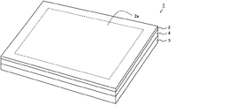
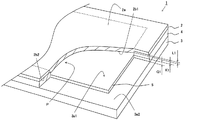
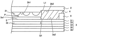
図1は、本発明を適用した一実施形態のフラットディスプレイパネルを右斜め上方から示す斜視図である。図2は、図1の部分断面図である。本実施形態のフラットディスプレイパネル1は、タッチパネルや3Dパネル等の基板状部材2が液晶表示パネル基板3上に接着剤4を用いて貼り合わせられている(図1)。そして、液晶表示パネル基板3の画像表示エリア(図中の符号2aに対応するエリア)に液晶表示パネル基板3よりも外周の小さなシート状フィルタ(偏光板)5が貼り合わされて段差Q1となり、液晶表示パネル基板3の画像表示エリア(図中の符号2aに対応)の外周に、接着剤塗布ガイドとしての段差部3a2が形成されている。また、基板状部材2の画像表示エリアの反対側の面のエリア2b1(図中の符号2aに対応するエリア)の外周に段差L1が形成されることで、貼り合せの際の接着剤ガイドとしての段差部2b2が形成されている。そして、基板状部材2の画像表示エリアの反対側の面のエリア2b1と液晶表示パネル基板3の画像表示エリア3a1とは、周回塗布された接着剤4によって所定の間隔K1を有する閉空間Pが形成されている(図2)。
(Configuration of flat display panel)
FIG. 1 is a perspective view showing a flat display panel according to an embodiment to which the present invention is applied from an obliquely upper right side. FIG. 2 is a partial cross-sectional view of FIG. In the
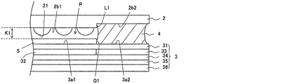
図3は、上記実施形態のフラットディスプレイパネルを側面側から見た部分断面図である。液晶表示パネル3は、一対の透明基板、すなわち対向基板31とアレイ基板34の間に液晶32が挟持され、液晶層32の周囲がシール材33で封止される。一対の透明基板31と34としては主にガラス基板が用いられる。一対の透明基板31と34の前後には、特定の偏光方向の光のみを透過させる偏光板(シート状フィルタ)5と35がそれぞれ配される。偏光板35の背面側(図3では下側)にはバックライト36が配される。画像表示面側の偏光板5の外周が透明基板31よりも小さく設定されることで、偏光板5の厚みによって段差Q1が形成される。つまり、透明基板31の画像表示エリア3a1に偏光板5が貼り合わされて段差Q1となり、透明基板31の画像表示エリア3a1の外周に、接着剤塗布ガイドとしての段差部3a2が形成される。段差部3a2は、周回塗布された接着剤4が画像表示エリア3a1に流れ込まないように制限するためのものである。
FIG. 3 is a partial cross-sectional view of the flat display panel of the above embodiment as viewed from the side. In the liquid
図3に示す本実施形態の基板状部材2は、3Dパネルであり、板ガラス2に半球形状のレンズ部材21がアレイ状に配列されている。図3では、液晶表示パネル3の内面側にレンズ部材21が配されているが、液晶表示パネル3の外面側にレンズ部材21が配されているものや、液晶表示パネル3の外面側と内面側の両方にレンズ部材21が配されているものもある。基板状部材2の画像表示エリアの反対側の面のエリア2b1の外周には、段差L1が形成され、貼り合せの際の接着剤ガイドとしての段差部2b2となる。段差部2b2は、周回塗布された接着剤4が画像表示エリアの反対側の面のエリア2b1に流れ込まないように制限するためのものである。そして、基板状部材2の画像表示エリアの反対側の面のエリアと液晶表示パネル基板3の画像表示エリアとは、周回塗布された接着剤4によって所定の間隔K1を有する閉空間Pが形成されている(図3)。
The substrate-
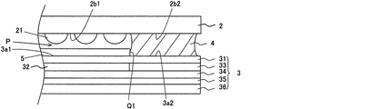
図4は、図3に示す上記実施形態の基板状部材2に段差L1を設けない場合の実施例である。例えば、高粘度の接着剤4を用いる場合、基板貼り合わせの際に接着剤4を押しつぶしたときの流動量が小さいため、基板状部材2側の段差L1を設ける必要はない。また例えば、段差部の隙間に対して接着剤4の量が比較的少ない場合には基板状部材2側の段差L1を設ける必要はない。そのため図4に示す実施例では、市販の基板状部材2を後加工することなく、液晶表示パネル3に貼り合わせることができる。
FIG. 4 shows an example in which the step L1 is not provided in the substrate-
図5は、図3に示す上記実施形態の透明基板31の外周付近の内周にスペーサ6を配する場合の実施例である。スペーサ6は、偏光板5の周囲に間隔をおいて配される。スペーサ6は、周回塗布された接着剤4が液晶表示パネル基板3の外側にはみ出さないように制限するためのものである。基板状部材2を透明基板31に貼り合わせた状態で、スペーサ6と基板状部材2の間には、若干の隙間があり、この隙間は、貼り合せの際に段差部2b2と段差部3a2との間に空気が閉じ込められることを防ぎ、接着剤4が空気を外に押し出す役割をする。
FIG. 5 shows an example in which the spacer 6 is arranged on the inner periphery in the vicinity of the outer periphery of the
(フラットディスプレイパネルの製造方法)
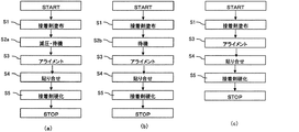
図6は、本発明のフラットディスプレイパネル1の製造手順を示す工程フローチャートである。図6(a)に示す工程フローチャートによる本実施形態の製造手順は、接着剤塗布工程(S1)、減圧・待機工程(S2a)、アライメント工程(S3)、貼り合せ工程(S4)、接着剤硬化工程(S5)からなる。接着剤塗布工程(S1)は、ディスペンサNによって接着剤4を周回塗布する。減圧・待機工程(S2a)は、接着剤4の塗布終了後、数分間程度待機して、接着剤4の塗布終了直後から接着剤4の高さが設定範囲内に収まるまで所定の待ち時間を設けるとともに、この待機時間を利用して真空チャンバーFによって減圧する。アライメント工程(S3)は、基板状部材2と画像表示パネル基板3とを対応する所定の貼り合せ位置に位置合わせする。貼り合せ工程(S4)は、基板状部材2と画像表示パネル基板3とを所定の貼り合せ位置で接着剤4を介して貼り合せする。接着剤硬化工程(S5)は、貼り合わされた基板状部材2と画像表示パネル基板3の接着剤4を加熱やUV照射等の手段で硬化する。ここで図6(a)と図6(b)と図6(c)との違いは、図6(a)では減圧しながら待機し(S2a)、図6(b)では減圧せずに待機し(S2b)、図6(c)では減圧も待機もしない点が異なる。
(Flat display panel manufacturing method)
FIG. 6 is a process flowchart showing the manufacturing procedure of the
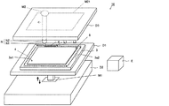
接着剤塗布工程(図6のS1)は、ディスペンサNによって接着剤4を周回塗布する。図7は、本発明のフラットディスプレイパネルの製造装置を示す斜視図であり、接着剤4を周回塗布する作業を示している。図7は、本発明のフラットディスプレイパネルの製造装置を示す斜視図であり、接着剤4を周回塗布する作業を示している。本実施形態の製造装置10では、基台D2の上方に液晶表示パネル基板3を載置して吸着するテーブルD1がスライド式の昇降機構によって連結され、昇降手段M1によって上下に昇降動作する。液晶表示パネル基板3は、真空吸引手段によってテーブルD1に吸着される。テーブルD1の上方には、ディスペンサNを吊り下げた天板D3がテーブルD1に対向配置される。ディスペンサNは、流動性のある接着剤4をシリンジN2に詰めて圧送し、ノズルN1の先端から接着剤4を吐出させて、接着剤4を偏光板5の外周に形成された段差部3a2に沿って周回塗布する。ディスペンサNは、ガイドレールM21に沿って周回移動する周回手段M2に連結され、周回動作する。本実施形態の製造装置10では、制御手段Eによって周回動作するノズルNと昇降動作するテーブルD1との組み合わせによって、画像表示パネル基板3の画像表示エリア3a1の外周に形成された段差部3a2を接着剤塗布ガイドとしてこの段差部3a2に沿って接着剤4を連続的に塗布させながら周回させ、テーブルD1を徐々に上昇させて行き、接着剤4の塗布開始から塗布終了にかけて段差部3a2とノズルN1の先端との間隔を徐々に縮めてゆく。又は、テーブルD1を昇降動作させずに、設定位置に固定させて、制御手段Eによって周回動作するノズルNによって、画像表示パネル基板3の画像表示エリア3a1の外周に形成された段差部3a2を接着剤塗布ガイドとしてこの段差部3a2に沿って接着剤4を連続的に塗布させながら周回させる。ノズルNは、段差部3a2に沿って1周し、接着剤4の塗布開始地点L1と接着剤4の塗布中間地点L2と接着剤4の塗布終了地点L3が連続するとともに、接着剤4の塗布開始地点L1と接着剤4の塗布終了地点L3が連結する。図7では、塗布された接着剤4が四角の枠状になる。本実施形態では、長方形状の液晶表示パネル基板3に形成された四角枠状の段差部3a2の長辺側の中央付近が、接着剤4の塗布開始地点L1となっている(図7)。これは、四角枠状の段差部3a2の四隅や短辺側に比べて四角枠状の段差部3a2の長辺側の中央付近が、接着剤4の塗布開始や塗布終了での塗布変動の影響を受け難いためである。
In the adhesive application step (S1 in FIG. 6), the adhesive 4 is applied by the dispenser N. FIG. 7 is a perspective view showing the flat display panel manufacturing apparatus of the present invention, and shows the operation of applying the adhesive 4 in a circular manner. FIG. 7 is a perspective view showing the flat display panel manufacturing apparatus of the present invention, and shows the operation of applying the adhesive 4 in a circular manner. In the
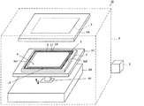
減圧・待機工程(図6のS2a)は、接着剤4の塗布終了後、数分間程度待機することで、接着剤4の塗布終了直後から接着剤4の高さが設定範囲内に収まるまで所定の待ち時間を設けるとともに、この待機時間を利用して真空チャンバーFによって減圧する。そして、基板状部材2と画像表示パネル基板3とを対応する所定の貼り合せ位置に位置合わせし(図6のS3)、基板状部材2と画像表示パネル基板3とを所定の貼り合せ位置で接着剤4を介して貼り合せする(図6のS4)。図8は、本発明のフラットディスプレイパネルの製造装置を示す斜視図であり、接着剤4の塗布終了後、基板状部材2と液晶表示パネル基板3を貼り合わせる前に減圧する減圧作業を示している。本実施形態の製造装置10では、天板D3の位置を横方向にずらして、貼り合せ対象である基板状部材2を上方から吊り下げて真空吸引手段によって吸着させる吸着ヘッドD4をテーブルD1の真上に配する。そして、接着剤4の塗布終了後に、制御手段EによってテーブルD1を徐々に上昇させて行き、吸着ヘッドD4とテーブルとの間隔を徐々に縮めてゆくことで、画像表示パネル基板3と基板状部材2とを対応する貼り合せ位置で貼り合わせて接着する。この貼り合せ作業は、真空チャンバーF内で行われる。大気圧下で接着剤4が塗布された後、制御手段Eによって真空チャンバーF内が減圧され、減圧下で基板状部材2と画像表示パネル基板3とが貼り合わされる(図6のS4)。例えば、接着剤4が熱硬化性接着剤である場合、接着剤硬化工程(図6のS5)では、接着剤4を加熱硬化するが、減圧下で基板状部材2と画像表示パネル基板3とを貼り合わせることで、図3や図4等に示す閉空間Pの加熱硬化の際の温度上昇による膨張が抑えられ、周回塗布された接着剤層4に貫通穴が生じることがなく、基板状部材2と液晶表示パネル3との間隔(ギャップ)が設定値からずれ難い。例えば、UV硬化性接着剤4を用いることで接着剤4を加熱しないで硬化させる場合には、減圧しなくてもよいため、図6(b)の工程フローとしてもよい。ただし、製品として完成後の使用環境下での熱の影響により閉空間Pの内部気体が膨張収縮することで、基板状部材2と液晶表示パネル3とのギャップが変動する恐れは残るので、製品として完成後の使用環境下での精密なギャップ寸法が要求される場合には図6(a)の工程フローが望ましい。また、後述する接着剤4の塗布及び貼り合せ条件によっては、待機工程を省いた図6(c)の工程フローとなる。
The depressurization / standby step (S2a in FIG. 6) waits for a few minutes after the application of the adhesive 4 is completed, and is predetermined until the height of the adhesive 4 falls within the set range immediately after the application of the adhesive 4 is completed. And the pressure is reduced by the vacuum chamber F using this waiting time. Then, the substrate-
上記実施の形態では、画像表示パネル基板3に接着剤4を連続的に塗布させながら周回させる例で説明したが、基板状部材2に接着剤4を連続的に塗布させながら周回させてもよい。この場合は、貼り合せ対象である画像表示パネル基板3を上方から吊り下げて吸着させる。
In the above-described embodiment, the example in which the adhesive 4 is continuously applied to the image
(実施例1)
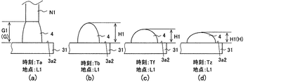
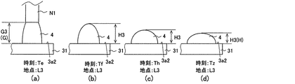
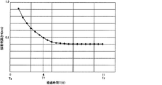
画面サイズが12.1インチの液晶表示パネル基板3の段差部3a2に沿って、ノズルN1からUV硬化型の接着剤4をガラス基板31に周回塗布した。図8に示す塗布開始地点L1から塗布終了地点L3までの周回距離は約900mmであり、ノズルN1の移動速度は約4mm/秒であるため、周回塗布に要する時間は約4分である。塗布開始地点L1でのノズルN1とガラス基板31との間隔G1と塗布終了地点L3での間隔G3は同一に設定し、1.0mmに固定した(G1=G3=1.0)。図9と図10は、ガラス基板31上に塗布された接着剤4の側断面の経時的変化を模式的に示している。ここで、図9は塗布開始地点L1での接着剤4の側断面の経時的変化を示しており、図10は塗布終了地点L3での接着剤4の側断面の経時的変化を示している。接着剤高さH1,H3は、時間の経過にともない、その高さが低くなってゆくが、徐々に高さが低くなる度合いが小さくなり、ある程度の時間が経過すると高さが一定してくる。図11は、塗布開始地点L1での時間経過にともなう接着剤4の接着剤高さH1をプロットしたグラフである。
Example 1
A UV
一般に接着剤の流動は、時間に対して線形ではない。図11に示すグラフに基づき接着剤高さH1の高さの変化率を計算した結果、接着剤塗布後最初の5分では接着剤高さH1の高さの変化率は約20%であるが、その後の5分ではおよそ5%以内の変化率となる。そして、さらに7分経過すると接着剤高さH1の高さの変化率は1%以内となる。よって、接着剤塗布終了後直ちに貼り合せを行った場合には、従来工法では接着剤高さH1とH3との高さの差が約18%となってしまうが、接着剤塗布終了後から7分間の待機時間を設けて貼り合せを行うことで、接着剤高さH1とH3との高さの差を3%以内に抑えることができた。この7分間の待機時間を利用して、真空チャンバーFによって減圧する他、基板状部材2を吸着ヘッドD4にセットする等の段取り作業を行うことができる。そして、3Dパネル2を液晶表示パネル基板3に貼り合せて、接着剤4を硬化させた。接着剤4を硬化させた後、接着剤層4を観察したところ、貫通穴はなく、室温にて内部に大気圧よりも低い気圧の閉空間Pを持つフラットディスプレイパネル1となった。
In general, adhesive flow is not linear with time. As a result of calculating the change rate of the height of the adhesive height H1 based on the graph shown in FIG. 11, the change rate of the height of the adhesive height H1 is about 20% in the first 5 minutes after applying the adhesive. In the next 5 minutes, the rate of change is within about 5%. Then, after 7 minutes have passed, the rate of change in the height of the adhesive height H1 is within 1%. Therefore, when bonding is performed immediately after the application of the adhesive is completed, the difference in height between the adhesive heights H1 and H3 is about 18% in the conventional method. By performing the bonding with a waiting time of minutes, the difference in height between the adhesive heights H1 and H3 could be suppressed to within 3%. Using the waiting time of 7 minutes, in addition to reducing the pressure by the vacuum chamber F, it is possible to perform setup operations such as setting the substrate-
(実施例2)
接着剤4の塗布開始地点L1でのノズルN1とガラス基板31との間隔G1に対して、塗布終了地点L3での間隔G3を縮める設定とした(G1>G3)。図11に示すグラフに基づき、所定時間経過後のノズルN1とガラス基板31との間隔GGを計算で求め、ノズルN1とガラス基板31との間隔Gを徐々に縮めてゆく設定とし、接着剤塗布終了後直ちに貼り合せを行った。接着剤4の貼り合せは減圧下で実施した。その他の設定条件は、実施例1と同一である。接着剤4の塗布開始地点L1でのノズルN1とガラス基板31との間隔G1は1.0mmであり、塗布開始地点L1での塗布直後の接着剤高さH1は0.95mmである。接着剤4の塗布終了地点L3での塗布開始からの経過時間は約4分であり、そのときの塗布開始地点L1での接着剤高さH1は0.8mmであり(図11)、接着剤4の塗布終了地点L3でのノズルN1とガラス基板31との間隔G3を0.8mmとする。また、接着剤4の塗布中間地点L2での塗布開始からの経過時間は約2分であり、そのときの塗布開始地点L1での接着剤高さH1は0.83mmであり(図11)、接着剤4の塗布中間地点L2でのノズルN1とガラス基板31との間隔G2を0.83mmとする。そして、接着剤塗布終了後直ちに3Dパネル2を液晶表示パネル基板3に貼り合せて、接着剤4を硬化させた。接着剤4を硬化させた後、接着剤層4を観察したところ、貫通穴はなく、室温にて内部に大気圧よりも低い気圧の閉空間Pを持つフラットディスプレイパネル1となった。なお、接着剤高さHは、接着剤4の材質、基板31の材料、塗布量、室温等の影響を受けるので、設定条件ごとに先行確認して図11と同様のグラフをプロットする。
(Example 2)
The gap G3 at the application end point L3 is set to be shorter than the gap G1 between the nozzle N1 and the
上述の実施例では、画面サイズが12.1インチの液晶表示パネル基板3に基板状部材(3Dパネル)2を貼り合わせた例を示したが、本発明によれば、画面サイズが大きくなればなるほど、従来に比べて貼り合わせの高精度が図られる実益が大きい。また、液晶表示パネル基板3の段差部3a2や基板状部材2の段差部2b2の表面粗さを適宜大きくすることで、接着剤4の接着力を高めることができる。このように、本発明は、その趣旨を逸脱しない範囲で適宜変更が可能であることは言うまでもない。
In the above-described embodiment, the example in which the substrate-like member (3D panel) 2 is bonded to the liquid crystal
1 フラットディスプレイパネル、
2 基板状部材(3Dパネル)、2b2 段差部、
3 画像表示パネル基板(液晶表示パネル基板)、3a2 段差部、
4 接着剤、
5 シート状フィルタ(偏光板)、
N ディスペンサ、 N1 ノズル、
G ノズル先端と基板との間隔、
H 接着剤高さ、
T 経過時間、
10 フラットディスプレイパネルの製造装置、
D1 テーブル、 D3 天板
1 flat display panel,
2 substrate-like member (3D panel), 2b2 stepped part,
3 Image display panel substrate (liquid crystal display panel substrate), 3a2, stepped portion,
4 Adhesive,
5 Sheet filter (polarizing plate),
N dispenser, N1 nozzle,
G Gap between nozzle tip and substrate,
H Adhesive height,
T elapsed time,
10 Flat display panel manufacturing equipment,
D1 table, D3 top plate
Claims (9)
接着剤位置決めガイドとしての段差部が前記画像表示パネル基板及び前記基板状部材の画像表示エリアの外周に向かい合って形成され、少なくとも一方の前記段差部の全周に前記接着剤が塗布されて、前記基板状部材と前記画像表示パネル基板とが貼り合わされていることを特徴とするフラットディスプレイパネル。 A flat display panel in which a substrate-like member and an image display panel substrate are bonded using an adhesive,
A step portion as an adhesive positioning guide is formed facing the outer periphery of the image display area of the image display panel substrate and the substrate-like member, and the adhesive is applied to the entire periphery of at least one of the step portions, A flat display panel, wherein a substrate-like member and the image display panel substrate are bonded together.
前記接着剤の塗布対象である前記画像表示パネル或いは前記基板状部材を載置して吸着するテーブルと、その上方に配され前記接着剤を下方に向けて塗布するノズルとを備え、制御手段によって前記ノズルと前記テーブルとを相対動作させて、前記画像表示パネル基板又は前記基板状部材の画像表示エリアの外周に形成された前記段差部を接着剤塗布ガイドとしてこの段差部に沿って接着剤を連続的に塗布させながら周回させ、
前記接着剤の塗布開始から塗布終了にかけて前記テーブルと前記ノズルの先端との間隔を徐々に縮めてゆき塗布終了後直ちに前記基板状部材と前記画像表示パネル基板とを貼り合わせることを特徴とするフラットディスプレイパネルの製造方法。 A method for producing a flat display panel in which a substrate-like member and an image display panel substrate are bonded together using an adhesive,
A table on which the image display panel or the substrate-like member to which the adhesive is to be applied is placed and adsorbed; and a nozzle that is disposed above and applies the adhesive downward. The nozzle and the table are relatively moved so that the step formed on the outer periphery of the image display area of the image display panel substrate or the substrate-like member is used as an adhesive application guide, and the adhesive is applied along the step. Circulate while applying continuously,
The distance between the table and the nozzle tip is gradually reduced from the start of application of the adhesive to the end of application, and the substrate-like member and the image display panel substrate are bonded immediately after the end of application. Display panel manufacturing method.
前記接着剤の塗布対象である前記画像表示パネル或いは前記基板状部材を載置して吸着するテーブルと、その上方に配され前記接着剤を下方に向けて塗布するノズルとを備え、制御手段によって前記ノズルと前記テーブルとを相対動作させて、前記画像表示パネル基板又は前記基板状部材の画像表示エリアの外周に形成された前記段差部を接着剤塗布ガイドとしてこの段差部に沿って接着剤を連続的に塗布させながら周回させ、
前記接着剤の塗布終了直後から接着剤の高さが設定範囲内に収まるまで所定の待ち時間を設けてから前記基板状部材と前記画像表示パネル基板とを貼り合わせることを特徴とするフラットディスプレイパネルの製造方法。 A method for producing a flat display panel in which a substrate-like member and an image display panel substrate are bonded together using an adhesive,
A table on which the image display panel or the substrate-like member to which the adhesive is to be applied is placed and adsorbed; and a nozzle that is disposed above and applies the adhesive downward. The nozzle and the table are relatively moved so that the step formed on the outer periphery of the image display area of the image display panel substrate or the substrate-like member is used as an adhesive application guide, and the adhesive is applied along the step. Circulate while applying continuously,
A flat display panel characterized in that the substrate-like member and the image display panel substrate are bonded together after providing a predetermined waiting time from the end of application of the adhesive until the height of the adhesive falls within a set range. Manufacturing method.
Priority Applications (1)
| Application Number | Priority Date | Filing Date | Title |
|---|---|---|---|
| JP2008291709A JP5173757B2 (en) | 2008-11-14 | 2008-11-14 | Flat display panel and manufacturing method of flat display panel |
Applications Claiming Priority (1)
| Application Number | Priority Date | Filing Date | Title |
|---|---|---|---|
| JP2008291709A JP5173757B2 (en) | 2008-11-14 | 2008-11-14 | Flat display panel and manufacturing method of flat display panel |
Publications (2)
| Publication Number | Publication Date |
|---|---|
| JP2010117618A true JP2010117618A (en) | 2010-05-27 |
| JP5173757B2 JP5173757B2 (en) | 2013-04-03 |
Family
ID=42305318
Family Applications (1)
| Application Number | Title | Priority Date | Filing Date |
|---|---|---|---|
| JP2008291709A Active JP5173757B2 (en) | 2008-11-14 | 2008-11-14 | Flat display panel and manufacturing method of flat display panel |
Country Status (1)
| Country | Link |
|---|---|
| JP (1) | JP5173757B2 (en) |
Cited By (2)
| Publication number | Priority date | Publication date | Assignee | Title |
|---|---|---|---|---|
| JP2013015760A (en) * | 2011-07-06 | 2013-01-24 | Shibaura Mechatronics Corp | Adhesive supply device and adhesive supply method |
| JP2014529769A (en) * | 2011-09-05 | 2014-11-13 | トビス カンパニー リミテッドTovisco., Ltd. | Curved display panel manufacturing method |
Families Citing this family (2)
| Publication number | Priority date | Publication date | Assignee | Title |
|---|---|---|---|---|
| JP7401279B2 (en) | 2019-12-06 | 2023-12-19 | 株式会社アドバンテック | Stage for heating and cooling objects |
| JP7458337B2 (en) | 2021-02-09 | 2024-03-29 | 株式会社アドバンテック | Stage for heating and cooling objects |
Citations (10)
| Publication number | Priority date | Publication date | Assignee | Title |
|---|---|---|---|---|
| JPS5380241A (en) * | 1976-12-24 | 1978-07-15 | Seiko Instr & Electronics Ltd | Liquid crystal panel |
| JPH07159795A (en) * | 1993-12-01 | 1995-06-23 | Fujitsu Ltd | Liquid crystal display panel manufacturing method |
| JPH11352897A (en) * | 1998-06-08 | 1999-12-24 | Mitsubishi Electric Corp | Flat panel display device and plasma display device |
| JP2000260304A (en) * | 1999-03-10 | 2000-09-22 | Canon Inc | Flat panel display |
| JP2004038581A (en) * | 2002-07-03 | 2004-02-05 | Seiko Instruments Inc | Display device and manufacturing method thereof |
| JP2006058605A (en) * | 2004-08-20 | 2006-03-02 | Seiko Epson Corp | Electro-optical device and electronic apparatus |
| JP2006343921A (en) * | 2005-06-08 | 2006-12-21 | Seiko Epson Corp | Method for manufacturing touch panel and method for manufacturing electro-optical device |
| JP2007328027A (en) * | 2006-06-06 | 2007-12-20 | Mitsubishi Electric Corp | Liquid crystal display device and manufacturing method thereof |
| JP2008009189A (en) * | 2006-06-29 | 2008-01-17 | Sharp Corp | Display device |
| JP2008090330A (en) * | 2007-12-25 | 2008-04-17 | Shibaura Mechatronics Corp | Adhesive coating apparatus, liquid crystal display panel, liquid crystal display panel manufacturing apparatus and manufacturing method, and substrate bonding apparatus |
-
2008
- 2008-11-14 JP JP2008291709A patent/JP5173757B2/en active Active
Patent Citations (10)
| Publication number | Priority date | Publication date | Assignee | Title |
|---|---|---|---|---|
| JPS5380241A (en) * | 1976-12-24 | 1978-07-15 | Seiko Instr & Electronics Ltd | Liquid crystal panel |
| JPH07159795A (en) * | 1993-12-01 | 1995-06-23 | Fujitsu Ltd | Liquid crystal display panel manufacturing method |
| JPH11352897A (en) * | 1998-06-08 | 1999-12-24 | Mitsubishi Electric Corp | Flat panel display device and plasma display device |
| JP2000260304A (en) * | 1999-03-10 | 2000-09-22 | Canon Inc | Flat panel display |
| JP2004038581A (en) * | 2002-07-03 | 2004-02-05 | Seiko Instruments Inc | Display device and manufacturing method thereof |
| JP2006058605A (en) * | 2004-08-20 | 2006-03-02 | Seiko Epson Corp | Electro-optical device and electronic apparatus |
| JP2006343921A (en) * | 2005-06-08 | 2006-12-21 | Seiko Epson Corp | Method for manufacturing touch panel and method for manufacturing electro-optical device |
| JP2007328027A (en) * | 2006-06-06 | 2007-12-20 | Mitsubishi Electric Corp | Liquid crystal display device and manufacturing method thereof |
| JP2008009189A (en) * | 2006-06-29 | 2008-01-17 | Sharp Corp | Display device |
| JP2008090330A (en) * | 2007-12-25 | 2008-04-17 | Shibaura Mechatronics Corp | Adhesive coating apparatus, liquid crystal display panel, liquid crystal display panel manufacturing apparatus and manufacturing method, and substrate bonding apparatus |
Cited By (3)
| Publication number | Priority date | Publication date | Assignee | Title |
|---|---|---|---|---|
| JP2013015760A (en) * | 2011-07-06 | 2013-01-24 | Shibaura Mechatronics Corp | Adhesive supply device and adhesive supply method |
| JP2014529769A (en) * | 2011-09-05 | 2014-11-13 | トビス カンパニー リミテッドTovisco., Ltd. | Curved display panel manufacturing method |
| US9523875B2 (en) | 2011-09-05 | 2016-12-20 | Tovis Co., Ltd. | Method for manufacturing curved-surface display |
Also Published As
| Publication number | Publication date |
|---|---|
| JP5173757B2 (en) | 2013-04-03 |
Similar Documents
| Publication | Publication Date | Title |
|---|---|---|
| JP5550357B2 (en) | Display device with front window | |
| JP5288729B2 (en) | Liquid crystal display | |
| US20140226112A1 (en) | Method for manufacturing curved-surface display | |
| CN101118353B (en) | Liquid crystal display device | |
| TW200534011A (en) | Substrate with spacer, panel, liquid crystal panel, method for producing panel, and method for producing liquid crystal panel | |
| JP2013504789A (en) | Curved display panel manufacturing method | |
| CN103261952A (en) | Method of manufacturing plate-haped bonded body, bonding device, and plate-shaped bonded body | |
| US20130016308A1 (en) | Liquid crystal display element, method for manufacturing same, and liquid crystal display device comprising the liquid crystal display element | |
| JP5173757B2 (en) | Flat display panel and manufacturing method of flat display panel | |
| WO2008007788A1 (en) | Structure and process for producing the same | |
| JP2016164617A (en) | Manufacturing method of liquid crystal cell, manufacturing method of light control material, and manufacturing method of laminated glass | |
| WO2012001864A1 (en) | Process for production of display device | |
| CN103913875B (en) | The automatic bonding system and automatic bonding method of liquid crystal display device | |
| TWI292065B (en) | Display device producing method and display device producing device | |
| KR101499987B1 (en) | Flexible liquid crystal display device and method of manufacturing the same | |
| JP2005128536A (en) | LIQUID CRYSTAL DISPLAY DEVICE, ITS MANUFACTURING METHOD, AND LIQUID CRYSTAL MANUFACTURING BONDING DEVICE | |
| JP2013174799A (en) | Polarizer sticking device and sticking method of polarizer using the same | |
| JP2010032775A (en) | Ferroelectric liquid crystal display element, and method of manufacturing the same | |
| TW201001028A (en) | Manufacturing method of alignment film and manufacturing method of liquid crystal display panel | |
| TW201530382A (en) | Touch panel, touch module and their bonding method | |
| TWI707939B (en) | Touchscreen having gel-based adhesive layer and method of manufacturing the same | |
| TWI313762B (en) | Module structure and assmebling method thereof | |
| TWI281580B (en) | Method of manufacture of LCD panel | |
| JP6237623B2 (en) | Glass film laminate | |
| US9250467B2 (en) | Manufacturing mold and manufacturing method for color filter |
Legal Events
| Date | Code | Title | Description |
|---|---|---|---|
| A621 | Written request for application examination |
Free format text: JAPANESE INTERMEDIATE CODE: A621 Effective date: 20110311 |
|
| A977 | Report on retrieval |
Free format text: JAPANESE INTERMEDIATE CODE: A971007 Effective date: 20120829 |
|
| A131 | Notification of reasons for refusal |
Free format text: JAPANESE INTERMEDIATE CODE: A131 Effective date: 20120906 |
|
| A521 | Request for written amendment filed |
Free format text: JAPANESE INTERMEDIATE CODE: A523 Effective date: 20121003 |
|
| TRDD | Decision of grant or rejection written | ||
| A01 | Written decision to grant a patent or to grant a registration (utility model) |
Free format text: JAPANESE INTERMEDIATE CODE: A01 Effective date: 20121206 |
|
| A61 | First payment of annual fees (during grant procedure) |
Free format text: JAPANESE INTERMEDIATE CODE: A61 Effective date: 20121227 |
|
| R150 | Certificate of patent or registration of utility model |
Ref document number: 5173757 Country of ref document: JP Free format text: JAPANESE INTERMEDIATE CODE: R150 |
|
| R250 | Receipt of annual fees |
Free format text: JAPANESE INTERMEDIATE CODE: R250 |
|
| R250 | Receipt of annual fees |
Free format text: JAPANESE INTERMEDIATE CODE: R250 |
|
| R250 | Receipt of annual fees |
Free format text: JAPANESE INTERMEDIATE CODE: R250 |
|
| R250 | Receipt of annual fees |
Free format text: JAPANESE INTERMEDIATE CODE: R250 |
|
| R250 | Receipt of annual fees |
Free format text: JAPANESE INTERMEDIATE CODE: R250 |
|
| R250 | Receipt of annual fees |
Free format text: JAPANESE INTERMEDIATE CODE: R250 |
|
| S111 | Request for change of ownership or part of ownership |
Free format text: JAPANESE INTERMEDIATE CODE: R313111 |
|
| R350 | Written notification of registration of transfer |
Free format text: JAPANESE INTERMEDIATE CODE: R350 |
|
| R250 | Receipt of annual fees |
Free format text: JAPANESE INTERMEDIATE CODE: R250 |
|
| R250 | Receipt of annual fees |
Free format text: JAPANESE INTERMEDIATE CODE: R250 |
|
| R250 | Receipt of annual fees |
Free format text: JAPANESE INTERMEDIATE CODE: R250 |
|
| R250 | Receipt of annual fees |
Free format text: JAPANESE INTERMEDIATE CODE: R250 |
|
| S111 | Request for change of ownership or part of ownership |
Free format text: JAPANESE INTERMEDIATE CODE: R313113 |
|
| R350 | Written notification of registration of transfer |
Free format text: JAPANESE INTERMEDIATE CODE: R350 |
|
| R250 | Receipt of annual fees |
Free format text: JAPANESE INTERMEDIATE CODE: R250 |