JP2010077378A - Double-faced adhesive film and electronic component module using the same - Google Patents
Double-faced adhesive film and electronic component module using the same Download PDFInfo
- Publication number
- JP2010077378A JP2010077378A JP2009001749A JP2009001749A JP2010077378A JP 2010077378 A JP2010077378 A JP 2010077378A JP 2009001749 A JP2009001749 A JP 2009001749A JP 2009001749 A JP2009001749 A JP 2009001749A JP 2010077378 A JP2010077378 A JP 2010077378A
- Authority
- JP
- Japan
- Prior art keywords
- film
- double
- adhesive film
- sided adhesive
- substrate
- Prior art date
- Legal status (The legal status is an assumption and is not a legal conclusion. Google has not performed a legal analysis and makes no representation as to the accuracy of the status listed.)
- Granted
Links
Images

Abstract
Description
本発明は、両面接着フィルム及びこれを用いた半導体パッケージ、MEMS(Micro Electro Mechanical Systems)モジュール等の電子部品モジュールに関する。 The present invention relates to a double-sided adhesive film, a semiconductor package using the same, and an electronic component module such as a MEMS (Micro Electro Mechanical Systems) module.
近年、半導体パッケージは高集積化・多様化してきており、特許文献1、2等に示されるように、1つのパッケージ内に同じ又は異なる半導体素子を2個以上搭載する場合が増えてきている。例えば、SIP(System In Package)のように、同一面上に搭載された2種類以上の半導体素子を有するパッケージにおいては、より高密度に搭載するために素子間の距離を可能な限り近づける必要がある。また、2個以上の半導体素子を重ねて積層する場合、接着フィルムの厚みを一定に保つ必要がある。
In recent years, semiconductor packages have been highly integrated and diversified, and as shown in
一方、センサー素子やMEMS素子の基板への搭載においては、素子の搭載位置の精度が重要である場合がある。また、センサー素子やMEMS素子等の2個以上の素子を基板に搭載する場合においては、隣り合う素子間の距離や搭載高さの違いを高い精度で制御することが重要である。 On the other hand, in mounting a sensor element or a MEMS element on a substrate, the accuracy of the mounting position of the element may be important. Further, when two or more elements such as a sensor element and a MEMS element are mounted on a substrate, it is important to control the difference between the adjacent elements and the mounting height with high accuracy.
例えば、2個以上のイメージセンサー素子を基板の同一面上に搭載する場合には、隣り合う素子間の距離及び素子の搭載高さのばらつきを最小限に抑える必要がある。そのため、素子の基板への搭載を高い位置精度で行う必要であるだけでなく、その後の加熱工程おいても搭載高さや素子間の位置関係が変化しないことが求められる。 For example, when two or more image sensor elements are mounted on the same surface of the substrate, it is necessary to minimize variations in the distance between adjacent elements and the mounting height of the elements. For this reason, it is necessary not only to mount the element on the substrate with high positional accuracy, but also to prevent the mounting height and the positional relationship between the elements from changing in the subsequent heating process.
しかし、基板の同一面上に複数の素子を従来の接着フィルムを用いて接着すると、加熱に伴う接着フィルムの変形に起因して、素子間の距離や素子の搭載高さが変化してしまうという問題があった。接着フィルムは、硬化、ワイヤボンディング、封止等のために基板又は素子に貼り付けられた状態で加熱される。従来の接着フィルムは、加熱されたときに、熱膨張、熱収縮、硬化収縮、揮発成分や吸湿水分の揮発による膨張などの変形を生じやすいという問題を有していた。特に、複数の素子が高密度に配置されるモジュールの製造においては、素子間の距離及び素子の搭載高さをより高い精度で制御することが求められるため、接着フィルムの変形を抑制することが非常に重要であることがわかった。 However, when a plurality of elements are bonded on the same surface of the substrate using a conventional adhesive film, the distance between elements and the mounting height of the elements change due to the deformation of the adhesive film accompanying heating. There was a problem. The adhesive film is heated while being attached to a substrate or an element for curing, wire bonding, sealing, or the like. Conventional adhesive films have a problem that when heated, they tend to cause deformation such as thermal expansion, thermal contraction, cure shrinkage, and expansion due to volatilization of volatile components and moisture absorption. In particular, in the manufacture of a module in which a plurality of elements are arranged at high density, it is required to control the distance between elements and the mounting height of the elements with higher accuracy, so that deformation of the adhesive film can be suppressed. It turned out to be very important.
さらには、複数の素子を基板に接着するために用いられる接着フィルムは、使用前に穴開け加工などによってその形状を加工することが必要とされる場合が多く、そのような加工によって発生するバリ等の異物が存在すると、接着強度の低下や素子の剥離の原因となり得ることから、異物の影響を抑制することも求められていた。 Furthermore, an adhesive film used for bonding a plurality of elements to a substrate is often required to be processed in shape by drilling before use, and a variability generated by such processing is required. The presence of foreign substances such as these can cause a decrease in adhesive strength and peeling of elements, so that it has also been desired to suppress the influence of foreign substances.
そこで、本発明は、複数の素子を基板に接着するための接着フィルムとして用いられたときに、穴開け等の加工に伴って発生する異物の影響を抑制できるとともに、加熱による変形が抑制された両面接着フィルムを提供することを主な目的とする。 Therefore, when the present invention is used as an adhesive film for adhering a plurality of elements to a substrate, it can suppress the influence of foreign matter that occurs during processing such as drilling, and the deformation due to heating is suppressed. The main purpose is to provide a double-sided adhesive film.
本発明は、支持フィルムと、該支持フィルムの両面にそれぞれ積層された接着剤層と、それぞれの該接着剤層の支持フィルムとは反対側の面に積層されたカバーフィルムと、を備える両面接着フィルムに関する。本発明に係る両面接着フィルムは、半導体素子及び/又はMEMS素子を基板に接着するために用いられる。 The present invention provides a double-sided adhesive comprising a support film, an adhesive layer laminated on both sides of the support film, and a cover film laminated on the surface of the adhesive layer opposite to the support film. Related to film. The double-sided adhesive film according to the present invention is used for bonding a semiconductor element and / or a MEMS element to a substrate.
本発明に係る両面接着フィルムは、両面接着フィルムを穴開け加工する工程と、穴開け加工された両面接着フィルムからカバーフィルムを除去する工程とを含む方法により、半導体素子及び/又はMEMS素子を基板に接着するために用いられる場合に特に有用である。この場合、穴開け加工された両面接着フィルムから、穴開け加工により生じた異物とともにカバーフィルムを除去することが好ましい。 The double-sided adhesive film according to the present invention is a method of forming a semiconductor element and / or a MEMS element on a substrate by a method including a step of perforating a double-sided adhesive film and a step of removing a cover film from the perforated double-sided adhesive film. It is particularly useful when used to adhere to. In this case, it is preferable to remove the cover film from the double-sided adhesive film that has been punched together with the foreign matter produced by the punching.
上記のような穴開け加工の工程を含む方法で素子を接着する場合に、本発明に係る両面接着フィルムを用いることによって、穴開け加工に伴って発生するバリ等の異物に起因する接着強度低下、信頼性低下などの不具合が十分に抑制される。例えば、穴開け加工に伴って発生する異物を一方の被着体に圧着する前にカバーフィルムを剥がして異物を除き、さらに他方の被着体を加熱圧着する前にもう一方のカバーフィルムを剥がして異物を除くことにより、異物に起因する不具合を防止することができる。 When the element is bonded by a method including the drilling process as described above, by using the double-sided adhesive film according to the present invention, the adhesive strength is reduced due to foreign matters such as burrs generated in the drilling process. In addition, problems such as a decrease in reliability are sufficiently suppressed. For example, remove the cover film before removing the foreign material generated by drilling to one adherend, and remove the other cover film before heat-pressing the other adherend. By removing the foreign matter, problems caused by the foreign matter can be prevented.
支持フィルムは100ppm以下の線膨張係数を有することが好ましい。加熱時の特性変化の少ない支持フィルムを用いることにより、素子を基板に搭載した後の接着フィルムの硬化工程、ワイヤボンディング工程及び封止工程等における加熱に伴う接着フィルムそのものの収縮及び膨張を更に効果的に抑制することができる。半導体素子やMEMS素子を構成する材料であるシリコン(Si)の線膨張係数は数ppmであり、一般的な基板、例えばガラスエポキシ基板、BT基板等の線膨張係数が数十ppmである。一方、従来の接着フィルムの線膨張係数は一般に数百ppmであり、基板と素子との線膨張係数の差、又は基板及び素子と接着フィルムとの線膨張係数の差により生じる反りを低減することが難しい。反りが発生すると、素子間の距離や素子の搭載高さが変化してしまう可能性がある。支持フィルムの線膨張係数を100ppm以下とすることで、効果的に反りを低減できる。 The support film preferably has a linear expansion coefficient of 100 ppm or less. By using a support film with little change in characteristics during heating, the shrinkage and expansion of the adhesive film itself due to heating in the curing process, wire bonding process, sealing process, etc. after mounting the device on the substrate is further effective Can be suppressed. Silicon (Si), which is a material constituting a semiconductor element or a MEMS element, has a coefficient of linear expansion of several ppm, and a general substrate such as a glass epoxy substrate or a BT substrate has a coefficient of linear expansion of several tens of ppm. On the other hand, the linear expansion coefficient of the conventional adhesive film is generally several hundred ppm, and the warpage caused by the difference in the linear expansion coefficient between the substrate and the element or the difference in the linear expansion coefficient between the substrate, the element and the adhesive film is reduced. Is difficult. When warping occurs, the distance between elements and the mounting height of the elements may change. Warpage can be effectively reduced by setting the linear expansion coefficient of the support film to 100 ppm or less.
硬化後の接着剤層は100℃未満のガラス転移温度(Tg)を有することが好ましい。接着剤層のガラス転移温度が低いと、接着フィルムを被着体に圧着する際の温度をより低くすることができる。例えば、一方の被着体(素子又は基板)に接着フィルムを圧着した後、さらに他方の被着体(基板又は素子)を圧着する方法により素子を基板に搭載する場合、接着フィルムを一方の被着体に圧着する際に、一般に接着フィルムをその硬化後のTg以上の温度に加熱しながら十分な圧力を加える必要がある。接着フィルムの被着体とは反対側の面は圧着用の治具と接触するため、加熱温度が高いと治具と接触する接着フィルムが変形して、その表面に微細な凹凸が形成されてしまう。接着フィルムの表面に微細な凹凸が形成されると、そこに他方の被着体を高精度で接着することが困難になるだけでなく、接着強度が低下する可能性もある。硬化後の接着剤層のTgが100℃未満であることで、このような問題の発生を防止することができる。 The cured adhesive layer preferably has a glass transition temperature (Tg) of less than 100 ° C. When the glass transition temperature of the adhesive layer is low, the temperature when the adhesive film is pressure-bonded to the adherend can be lowered. For example, when an element is mounted on a substrate by a method in which an adhesive film is pressure-bonded to one adherend (element or substrate) and then the other adherend (substrate or element) is further pressure-bonded, the adhesive film is attached to one adherend. When pressure-bonding to the adherend, it is generally necessary to apply sufficient pressure while heating the adhesive film to a temperature equal to or higher than Tg after curing. Since the surface of the adhesive film opposite to the adherend is in contact with the crimping jig, when the heating temperature is high, the adhesive film in contact with the jig is deformed, and fine irregularities are formed on the surface. End up. If fine irregularities are formed on the surface of the adhesive film, it is difficult not only to adhere the other adherend to the surface with high precision, but also the adhesive strength may be lowered. Generation | occurrence | production of such a problem can be prevented because Tg of the adhesive bond layer after hardening is less than 100 degreeC.
支持フィルムは、好ましくは、芳香族ポリイミド、芳香族ポリアミドイミド、芳香族ポリエーテルスルホン、ポリフェニレンスルフィド、芳香族ポリエーテルケトン、ポリアリレート、芳香族ポリエーテルケトン、ポリエチレンナフタレート及び液晶ポリマーからなる群から選ばれるポリマーのフィルムである。 The support film is preferably from the group consisting of aromatic polyimide, aromatic polyamideimide, aromatic polyethersulfone, polyphenylene sulfide, aromatic polyetherketone, polyarylate, aromatic polyetherketone, polyethylene naphthalate and liquid crystal polymer. A film of the polymer chosen.
それぞれの上記接着剤層は互いに同じ組成を有することが好ましい。また、それぞれの上記接着剤層は、100℃以下のガラス転移温度を有する熱可塑性樹脂と、熱硬化性樹脂と、フィラーとを含有することが好ましい。 Each of the adhesive layers preferably has the same composition. Moreover, it is preferable that each said adhesive bond layer contains the thermoplastic resin which has a glass transition temperature of 100 degrees C or less, a thermosetting resin, and a filler.
別の側面において、本発明は基板と、該基板に搭載された、半導体素子及びMEMS素子から選ばれる複数の素子と、基板と素子との間に介在する接着層と、を備える電子部品モジュールに関する。本発明に係る電子部品モジュールの接着層は、カバーフィルムが除去された上記本発明に係る両面接着フィルムから形成されている。 In another aspect, the present invention relates to an electronic component module comprising a substrate, a plurality of elements selected from semiconductor elements and MEMS elements mounted on the substrate, and an adhesive layer interposed between the substrate and the elements. . The adhesive layer of the electronic component module according to the present invention is formed from the double-sided adhesive film according to the present invention from which the cover film has been removed.
本発明に係る電子部品モジュールは、高い信頼性を達成することができ、また、高い生産性で製造されることが可能である。 The electronic component module according to the present invention can achieve high reliability and can be manufactured with high productivity.
本発明に係る両面接着フィルムは、複数の素子を基板に接着するための接着フィルムとして用いられたときに、穴開け等の加工に伴って発生する異物の影響を抑制できるとともに、加熱による変形が抑制される。 When the double-sided adhesive film according to the present invention is used as an adhesive film for adhering a plurality of elements to a substrate, it can suppress the influence of foreign matter that occurs during processing such as drilling, and can be deformed by heating. It is suppressed.
以下、本発明の好適な実施形態について詳細に説明する。ただし、本発明は以下の実施形態に限定されるものではない。 Hereinafter, preferred embodiments of the present invention will be described in detail. However, the present invention is not limited to the following embodiments.
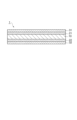
図1は、両面接着フィルムの一実施形態を示す断面図である。図1に示す両面接着フィルム1は、支持フィルム10と、支持フィルム10の両面にそれぞれ積層された2つの接着剤層21,22と、2つの接着剤層21,22それぞれの支持フィルム10とは反対側の面に積層されたカバーフィルム31,32とを備える5層構成の積層体である。
FIG. 1 is a cross-sectional view showing an embodiment of a double-sided adhesive film. A double-sided
本実施形態に係る両面接着フィルムは、例えば、両面接着フィルム1を穴開け加工する工程と、穴開け加工された両面接着フィルム1から一方のカバーフィルム31を除去し、一方の接着剤層21を一方の被着体(基板)に熱圧着する工程と、穴開け加工された両面接着フィルム1から他方のカバーフィルム32を除去し、他方の接着剤層22を他方の被着体(半導体素子及び/又はMEMS素子)に熱圧着する工程とを含む方法により、半導体素子及び/又はMEMS素子を基板に接着するために用いられる。一方のカバーフィルム31を除去して一方の被着体を両面接着フィルム1に熱圧着した後、他方のカバーフィルム32を除去して他方の被着体を両面接着フィルム1に熱圧着してもよいし、両方のカバーフィルム31,32を除去し、両被着体を両面接着フィルムに同時に熱圧着してもよい。
The double-sided adhesive film according to the present embodiment includes, for example, a step of punching the double-sided
両面接着フィルムの穴開け加工には、例えば、機械による穴開け、レーザー又はプラズマによる穴開けがある。穴開け加工によって、支持フィルム10及び接着剤層21,22とともにカバーフィルム31,32を貫通する貫通孔が形成される。
Examples of the punching process for the double-sided adhesive film include drilling by a machine and drilling by a laser or plasma. Through holes are formed through the
支持フィルム10は、加熱による特性変化の少ない材料から形成されることが好ましい。これにより、素子を基板に搭載した後の接着フィルムの硬化工程、ワイヤボンディング工程、封止工程等における加熱による両面接着フィルムそのものの加熱収縮及び膨張をより効果的に抑制することができる。
The
係る観点から、支持フィルム10のTgは100℃以上が好ましく、150℃以上がより好ましく、200℃以上がさらに好ましい。支持フィルム10の線膨張係数は、100ppm以下が好ましく、70ppm以下がより好ましく、50ppm以下がさらに好ましい。
From such a viewpoint, the Tg of the
上記のような特性を達成するため、支持フィルム10は、芳香族ポリイミド、芳香族ポリアミドイミド、芳香族ポリエーテルスルホン、ポリフェニレンスルフィド、芳香族ポリエーテルケトン、ポリアリレート、芳香族ポリエーテルケトン、ポリエチレンナフタレート及び液晶ポリマーからなる群から選ばれるポリマーのフィルムであることが好ましい。
In order to achieve the above characteristics, the
カバーフィルム31,32としては、例えば、ポリエチレンテレフタレート、ポリエチレン及びポリプロピレンからなる群から選ばれるポリマーのフィルムが用いられる。
As the
接着剤層21,22の硬化後のTgが低いと、熱圧着時の温度を低くして、接着フィルムに熱が過剰に加わることを回避して、接着フィルムの変形をより顕著に抑制することができる。具体的には、硬化後の接着剤層21,22のTgは100℃未満が好ましく、90℃未満がより好ましく、80℃未満がさらに好ましい。
If the Tg after curing of the
接着剤層21,22は、例えば、熱可塑性樹脂、熱硬化性樹脂及びフィラーをそれぞれ含有する。2つの接着剤層21,22の組成は互いに同一でも異なっていてもよいが、変形防止や反り防止の観点からは同一であることが好ましい。
The adhesive layers 21 and 22 contain, for example, a thermoplastic resin, a thermosetting resin, and a filler, respectively. The compositions of the two
熱可塑性樹脂のTgは好ましくは100℃未満、より好ましくは90℃未満、さらに好ましくは80℃未満である。Tgが低い熱可塑性樹脂を用いることにより、低いTgを有する接着剤層を容易に形成することができる。また、熱可塑性樹脂は、ポリイミド樹脂、ポリアミドイミド樹脂、ポリエーテルスルホン樹脂、ポリアクリレート樹脂、ポリエーテルケトン樹脂、ポリアリレート、ポリエーテルケトン及びポリエチレンナフタレートからなる群から選ばれる少なくとも1種であってもよい。 The Tg of the thermoplastic resin is preferably less than 100 ° C, more preferably less than 90 ° C, and even more preferably less than 80 ° C. By using a thermoplastic resin having a low Tg, an adhesive layer having a low Tg can be easily formed. The thermoplastic resin is at least one selected from the group consisting of polyimide resin, polyamideimide resin, polyethersulfone resin, polyacrylate resin, polyetherketone resin, polyarylate, polyetherketone, and polyethylene naphthalate. Also good.
熱硬化性樹脂は、3次元網目構造を形成し得る化合物である。熱硬化性樹脂は、通常、硬化剤及び/又は硬化促進剤の作用によって3次元網目構造を形成して硬化する。熱硬化性樹脂を用いることにより、高温での剪断接着力が高くなる傾向がある。ただし、熱硬化性樹脂を用いると高温でのピール接着力は逆に低下する可能性があるため、使用目的に応じて、熱硬化性樹脂の使用の有無を適宜選択するのがよい。 A thermosetting resin is a compound that can form a three-dimensional network structure. The thermosetting resin is usually cured by forming a three-dimensional network structure by the action of a curing agent and / or a curing accelerator. By using a thermosetting resin, the shear adhesive strength at high temperatures tends to increase. However, when a thermosetting resin is used, the peel adhesive strength at a high temperature may be reduced, and therefore it is preferable to appropriately select whether or not to use the thermosetting resin according to the purpose of use.
熱硬化性樹脂の量は、熱可塑性樹脂100質量部に対して、好ましくは1〜100質量部、より好ましくは1〜50質量部である。熱硬化性樹脂の量が100質量部を超えるとフィルム形成性が低下する傾向がある。 The amount of the thermosetting resin is preferably 1 to 100 parts by mass, more preferably 1 to 50 parts by mass with respect to 100 parts by mass of the thermoplastic resin. When the amount of the thermosetting resin exceeds 100 parts by mass, the film formability tends to decrease.
熱硬化性樹脂は、好ましくは、エポキシ樹脂及び2個の熱硬化性イミド基を有するイミド化合物から選ばれる。 The thermosetting resin is preferably selected from an epoxy resin and an imide compound having two thermosetting imide groups.
エポキシ樹脂は、1分子中に1個以上のエポキシ基を有する化合物であれば特に制限はない。エポキシ樹脂としては、例えば、アルキルモノグリシジルエーテル、フェニルグリシジルエーテル、アルキルフェノールモノグリシジルエーテル、3−グリシドキシプロピルトリメトキシシラン、3−グリシドキシプロピルメチルジメトキシシラン、1−(3−グリシドキシプロピル)-1,1,3,3,3−ペンタメチルジシロキサン、アルキルモノグリシジルエステル、ビスフェノールA型エポキシ樹脂[AER−X8501(旭化成エポキシ(株)、商品名)、R−301(三井化学(株)、商品名)、YL−980(ジャパンエポキシレジン(株)、商品名)]、ビスフェノールF型エポキシ樹脂[YDF−170(東都化成(株)、商品名)]、ビスフェノールAD型エポキシ樹脂[R−1710(三井化学(株)、商品名)]、フェノールノボラック型エポキシ樹脂[N−730S(大日本インキ化学工業(株)、商品名)、Quatrex−2010(ダウ・ケミカル社、商品名)]、ビスフェノールS型エポキシ樹脂、クレゾールノボラック型エポキシ樹脂[YDCN−702S(東都化成(株)、商品名)、EOCN−100(日本化薬(株)、商品名)]、多官能エポキシ樹脂[EPPN−501(日本化薬(株)、商品名)、TACTIX−742(ダウ・ケミカル社、商品名)、VG−3010(三井化学(株)、商品名)、1032S(ジャパンエポキシレジン(株)、商品名)]、ナフタレン骨格を有するエポキシ樹脂[HP−4032(大日本インキ化学工業(株)、商品名)]、ジシクロ型エポキシ樹脂[EP−4088S(旭電化工業(株)、商品名)、XD−1000−L(日本化薬(株)、商品名)]、脂環式エポキシ樹脂[EHPE−3150、CEL−3000(ダイセル化学工業(株)、商品名)、DME−100(新日本理化(株)、商品名)、EX−216L(ナガセケムテックス(株)、商品名)]、脂肪族エポキシ樹脂[W−100(新日本理化(株)、商品名)、YH−300(東都化成(株)、商品名)]、エポキシ化ポリブタジエン[PB−3600(ダイセル化学工業(株)、商品名)、E−1000−3.5(日本石油化学(株)、商品名)]、エポキシ化植物油[S−300K、L−500(ダイセル化学工業(株)、商品名)]、アミン型エポキシ樹脂[ELM−100(住友化工業(株)、商品名)、YH−434L(東都化成(株)、商品名)、TETRAD−X、TETRAD−C(三菱瓦斯化学(株)、商品名)、GOT、GAN(日本化薬(株)、商品名)]、エチレン/プロピレングリコール変性ビスフェノール型エポキシ樹脂[EP−4000S(旭電化工業(株)、商品名)、BEO−60E(新日本理化(株)、商品名)]、水素添加ビスフェノール型エポキシ樹脂[EXA−7015(日本化薬(株)、商品名)、ST−5080(東都化成(株)、商品名)]、レゾルシン型エポキシ樹脂[デナコールEX−201(ナガセケムテックス(株)、商品名)]、カテコール骨格を有するエポキシ樹脂[EXA−7120(大日本インキ化学工業(株)、商品名)]、ネオペンチルグリコール型エポキシ樹脂[デナコールEX−211(ナガセケムテックス(株)、商品名)]、ヘキサンディネルグリコール型エポキシ樹脂[デナコールEX−212(ナガセケムテックス(株)、商品名)]、エチレン/プロピレングリコール型エポキシ樹脂[デナコールEX−810、811、850、851、821、830、832、841、861(ナガセケムテックス(株)、商品名)]、ビフェニル型エポキシ樹脂[YX−4000H(ジャパンエポキシレジン(株)、商品名]、下記一般式(I) The epoxy resin is not particularly limited as long as it is a compound having one or more epoxy groups in one molecule. Examples of the epoxy resin include alkyl monoglycidyl ether, phenyl glycidyl ether, alkylphenol monoglycidyl ether, 3-glycidoxypropyltrimethoxysilane, 3-glycidoxypropylmethyldimethoxysilane, and 1- (3-glycidoxypropyl). ) -1,1,3,3,3-pentamethyldisiloxane, alkyl monoglycidyl ester, bisphenol A type epoxy resin [AER-X8501 (Asahi Kasei Epoxy Co., Ltd., trade name), R-301 (Mitsui Chemicals, Inc.) ), Trade name), YL-980 (Japan Epoxy Resin Co., Ltd., trade name)], bisphenol F type epoxy resin [YDF-170 (Toto Kasei Co., Ltd., trade name)], bisphenol AD type epoxy resin [R -1710 (Mitsui Chemicals, Inc., trade name)], F Enol novolak type epoxy resin [N-730S (Dainippon Ink and Chemicals, trade name), Quatrex-2010 (Dow Chemical Co., trade name)], bisphenol S type epoxy resin, cresol novolak type epoxy resin [YDCN -702S (Toto Kasei Co., Ltd., trade name), EOCN-100 (Nippon Kayaku Co., Ltd., trade name)], polyfunctional epoxy resin [EPPN-501 (Nippon Kayaku Co., Ltd., trade name), TACTIX -742 (Dow Chemical Company, trade name), VG-3010 (Mitsui Chemicals, trade name), 1032S (Japan Epoxy Resin Co., trade name)], epoxy resin having a naphthalene skeleton [HP-4032 (Dainippon Ink Chemical Co., Ltd., trade name)], dicyclo type epoxy resin [EP-4088S (Asahi Denka Kogyo Co., Ltd., quotient) Name), XD-1000-L (Nippon Kayaku Co., Ltd., trade name)], alicyclic epoxy resin [EHPE-3150, CEL-3000 (Daicel Chemical Industries, trade name), DME-100 ( Shin Nippon Rika Co., Ltd., trade name), EX-216L (Nagase ChemteX Corporation, trade name)], aliphatic epoxy resin [W-100 (New Nippon Rika Co., Ltd., trade name), YH-300 (Toto Kasei Co., Ltd., trade name)], epoxidized polybutadiene [PB-3600 (Daicel Chemical Industries, trade name), E-1000-3.5 (Nippon Petrochemical Co., Ltd., trade name)] Epoxidized vegetable oil [S-300K, L-500 (Daicel Chemical Industries, Ltd., trade name)], amine type epoxy resin [ELM-100 (Sumitomo Chemical Co., Ltd., trade name), YH-434L (Tokyo) Kasei Co., Ltd., trade name), ETRAD-X, TETRAD-C (Mitsubishi Gas Chemical Co., Ltd., trade name), GOT, GAN (Nippon Kayaku Co., Ltd., trade name)], ethylene / propylene glycol modified bisphenol type epoxy resin [EP-4000S (Asahi) Denka Kogyo Co., Ltd., trade name), BEO-60E (New Nippon Rika Co., Ltd., trade name)], hydrogenated bisphenol type epoxy resin [EXA-7015 (Nippon Kayaku Co., Ltd., trade name), ST- 5080 (Toto Kasei Co., Ltd., trade name)], resorcin-type epoxy resin [Denacol EX-201 (Nagase ChemteX Corporation, trade name)], epoxy resin having a catechol skeleton [EXA-7120 (Dainippon Ink Chemical Co., Ltd.) Kogyo Co., Ltd., trade name)], neopentyl glycol type epoxy resin [Denacol EX-211 (Nagase ChemteX Corporation, trade name) )], Hexane dinel glycol type epoxy resin [Denacol EX-212 (Nagase ChemteX Corp., trade name)], ethylene / propylene glycol type epoxy resin [Denacol EX-810, 811, 850, 851, 821, 830] 832, 841, 861 (Nagase ChemteX Corp., trade name)], biphenyl type epoxy resin [YX-4000H (Japan Epoxy Resin Co., Ltd., trade name)], the following general formula (I)

(式中、aは0〜5の整数を表す。)
で表されるエポキシ樹脂[E−XL−24、E−XL−3L(三井化学(株)、商品名)]、ウレタン変性エポキシ樹脂[EPU−15、EPU−18(旭電化工業(株)、商品名)]、ゴム変性エポキシ樹脂[EPR−4032、EPR−1309(旭電化工業(株)、商品名)]、キレート変性エポキシ樹脂[EP−49−10、EPU−78−11(旭電化工業(株)、商品名)]、グリシジルエステル型エポキシ樹脂[YD−171、YD−172(東都化成(株)、商品名)、AK−601(日本化薬(株)、商品名)]が挙げられる。
(Wherein, a represents an integer of 0 to 5)
[E-XL-24, E-XL-3L (Mitsui Chemicals, Inc., trade name)], urethane-modified epoxy resin [EPU-15, EPU-18 (Asahi Denka Kogyo Co., Ltd.), Product name)], rubber-modified epoxy resin [EPR-4032, EPR-1309 (Asahi Denka Kogyo Co., Ltd., product name)], chelate-modified epoxy resin [EP-49-10, EPU-78-11 (Asahi Denka Kogyo) (Trade name)], glycidyl ester type epoxy resin [YD-171, YD-172 (Toto Kasei Co., Ltd., trade name), AK-601 (Nippon Kayaku Co., Ltd., trade name)]. It is done.
これらのなかでも、ビスフェノールA型エポキシ樹脂、ビスフェノールF型エポキシ樹脂、ビスフェノールAD型エポキシ樹脂、フェノールノボラック型エポキシ樹脂、クレゾールノボラック型エポキシ樹脂及び脂環式エポキシ樹脂からなる群より選ばれる少なくとも1種のエポキシ樹脂を用いることが好ましい。これらのエポキシ樹脂は単独で又は2種以上を組み合わせて使用することができる。 Among these, at least one selected from the group consisting of bisphenol A type epoxy resins, bisphenol F type epoxy resins, bisphenol AD type epoxy resins, phenol novolac type epoxy resins, cresol novolac type epoxy resins, and alicyclic epoxy resins. It is preferable to use an epoxy resin. These epoxy resins can be used alone or in combination of two or more.
接着剤層21,22は、上記エポキシ樹脂と組み合わせて用いられる硬化剤を含有してもよい。硬化剤の例としては、フェノールノボラック樹脂[H−1(明和化成(株)、商品名)、VR−9300(三井化学(株)、商品名)]、フェノールアラルキル樹脂[XL−225(三井化学(株)、商品名)]、アリル化フェノールノボラック樹脂[AL−VR−9300(三井化学(株)、商品名)]、下記一般式(II) The adhesive layers 21 and 22 may contain a curing agent used in combination with the epoxy resin. Examples of the curing agent include phenol novolac resin [H-1 (Maywa Kasei Co., Ltd., trade name), VR-9300 (Mitsui Chemicals, trade name)], phenol aralkyl resin [XL-225 (Mitsui Chemicals). (Trade name)], allylated phenol novolak resin [AL-VR-9300 (Mitsui Chemicals, trade name)], the following general formula (II)
(式中、R1はメチル基、エチル基等の炭素数1〜6のアルキル基を示し、R2は水素又はメチル基、エチル基等の炭素数1〜6のアルキル基を示し、bは2〜4の整数を示す。)で表される特殊フェノール樹脂[PP−700−300(日本石油化学(株)製、商品名)]、ビスフェノールF、ビスフェノールA、ビスフェノールAD、ビスフェノールS、アリル化ビスフェノールF、アリル化ビスフェノールA、アリル化ビスフェノールAD、アリル化ビスフェノールS、多官能フェノール[p−CR、TrisP−PHBA、MTPC、TrisP−RS(本州化学工業(株)、商品名)]等のフェノール化合物、o−フェニレンジアミン、m−フェニレンジアミン、p−フェニレンジアミン、3,3’−ジアミノジフェニルエーテル、3,4’−ジアミノジフェニルエーテル、4,4’−ジアミノジフェニルエーテル、3,3’−ジアミノジフェニルメタン、3,4’−ジアミノジフェニルメタン、4,4’−ジアミノジフェニルメタン、3,3’−ジアミノジフェニルジフルオロメタン、3,4’−ジアミノジフェニルジフルオロメタン、4,4’−ジアミノジフェニルジフルオロメタン、3,3’−ジアミノジフェニルスルホン、3,4’−ジアミノジフェニルスルホン、4,4’−ジアミノジフェニルスルホン、3,3’−ジアミノジフェニルスルフイド、3,4’−ジアミノジフェニルスルフイド、4,4’−ジアミノジフェニルスルフイド、3,3’−ジアミノジフェニルケトン、3,4’−ジアミノジフェニルケトン、4,4’−ジアミノジフェニルケトン、2,2−ビス(3−アミノフェニル)プロパン、2,2’−(3,4’−ジアミノジフェニル)プロパン、2,2−ビス(4−アミノフェニル)プロパン、2,2−ビス(3−アミノフェニル)ヘキサフルオロプロパン、2,2−(3,4’−ジアミノジフェニル)ヘキサフルオロプロパン、2,2−ビス(4−アミノフェニル)ヘキサフルオロプロパン、1,3−ビス(3−アミノフェノキシ)ベンゼン、1,4−ビス(3−アミノフェノキシ)ベンゼン、1,4−ビス(4−アミノフェノキシ)ベンゼン、3,3’−(1,4−フェニレンビス(1−メチルエチリデン))ビスアニリン、3,4’−(1,4−フェニレンビス(1−メチルエチリデン))ビスアニリン、4,4’−(1,4−フェニレンビス(1−メチルエチリデン))ビスアニリン、2,2−ビス(4−(3−アミノフェノキシ)フェニル)プロパン、2,2−ビス(4−(4−アミノフェノキシ)フェニル)プロパン、2,2−ビス(4−(3−アミノフェノキシ)フェニル)ヘキサフルオロプロパン、2,2−ビス(4−(4−アミノフエノキシ)フェニル)ヘキサフルオロプロパン、ビス(4−(3−アミノフェノキシ)フェニル)スルフィド、ビス(4−(4−アミノフェノキシ)フェニル)スルフィド、ビス(4−(3−アミノフェノキシ)フェニル)スルホン、ビス(4−(4−アミノフェノキシ)フェニル)スルホン、1,2−ジアミノエタン、1,3−ジアミノプロパン、1,4−ジアミノブタン、1,5−ジアミノペンタン、ジエチレントリアミン、トリエチレンテトラミン、ジエチルアミノプロピルアミン、1,1,3,3−テトラメチル−1,3−ビス(4−アミノフェニル)ジシロキサン、1,1,3,3−テトラフェノキシ−1,3−ビス(4−アミノエチル)ジシロキサン、1,1,3,3−テトラフェニル−1,3−ビス(2−アミノエチル)ジシロキサン、1,1,3,3−テトラフェニル−1,3−ビス(3−アミノプロピル)ジシロキサン、1,1,3,3−テトラメチル−1,3−ビス(2−アミノエチル)ジシロキサン、1,1,3,3−テトラメチル−1,3−ビス(3−アミノプロピル)ジシロキサン、1,1,3,3−テトラメチル−1,3−ビス(3−アミノブチル)ジシロキサン、1,3−ジメチル−1,3−ジメトキシ−1,3−ビス(4−アミノブチル)ジシロキサン、1,1,3,3,5,5−ヘキサメチル−1,5−ビス(4−アミノフェニル)トリシロキサン、1,1,5,5−テトラフェニル−3,3−ジメチル−1,5−ビス(3−アミノプロピル)トリシロキサン、1,1,5,5−テトラフェニル−3,3−ジメトキシ−1,5−ビス(4−アミノブチル)トリシロキサン、1,1,5,5−テトラフェニル−3,3−ジメトキシ−1,5−ビス(5−アミノペンチル)トリシロキサン、1,1,5,5−テトラメチル−3,3−ジメトキシ−1,5−ビス(2−アミノエチル)トリシロキサン、1,1,5,5−テトラメチル−3,3−ジメトキシ−1,5−ビス(4−アミノブチル)トリシロキサン、1,1,5,5−テトラメチル−3,3−ジメトキシ−1,5−ビス(5−アミノペンチル)トリシロキサン、1,1,3,3,5,5−ヘキサメチル−1,5−ビス(3−アミノプロピル)トリシロキサン、1,1,3,3,5,5−ヘキサエチル−1,5−ビス(3−アミノプロピル)トリシロキサン、1,1,3,3,5,5−ヘキサプロピル−1,5−ビス(3−アミノプロピル)トリシロキサン、トリエチルアミン、ベンジルジメチルアミン、α−メチルベンジルジメチルアミン、トリスジメチルアミノメチルフェノール、ピペリジン、メンタンジアミン、ボロントリフルオライドモノエチルアミン、1,8−ジアザビシクロ[5.4.0]−ウンデセン−7、6−ブチル−1,8−ジアザビシクロ[5.4.0]−ウンデセン−7、1,5−ジアザビシクロ[4.3.0]−ノネン−5等のアミン化合物、ジシアンジアミド、二塩基酸ジヒドラジド[ADH、PDH、SDH(いずれも日本ヒドラジン工業(株)製、商品名)]、エポキシ樹脂とアミン化合物の反応物からなるマイクロカプセル型硬化剤[ノバキュア(旭化成工業(株)製、商品名)]、U−CAT3502T、U−CAT3503N(サンアプロ(株)、商品名)等の尿素化合物、無水フタル酸、無水マレイン酸、無水シトラコン酸、無水イタコン酸、無水コハク酸、無水ドデシルコハク酸、無水テトラヒドロフタル酸、無水ヘキサヒドロフタル酸、3又は4−メチル−1,2,3,6−テトラヒドロ無水フタル酸、3又は4−メチルヘキサヒドロ無水フタル酸、ビシクロ[2.2.1]へプト−5−エン−2,3−ジカルボン酸無水物、メチルビシクロ[2.2.1]へプト−5−エン−2,3−ジカルボン酸無水物、ピロメリット酸二無水物、3,3’,4,4’−ジフェニルテトラカルボン酸二無水物、2,2’,3,3’−ジフェニルテトラカルボン酸二無水物、2,2−ビス(3,4−ジカルボキシフェニル)プロパン二無水物、2,2−ビス(2,3−ジカルボキシフェニル)プロパン二無水物、1,1−ビス(2,3−ジカルボキシフェニル)エタン二無水物、1,1−ビス(3,4−ジカルボキシフェニル)エタン二無水物、ビス(2,3−ジカルボキシフェニル)メタン二無水物、ビス(3,4−ジカルボキシフェニル)メタン二無水物、ビス(3,4−ジカルボキシフェニル)スルホン二無水物、3,4,9,10−ペリレンテトラカルボン酸二無水物、ビス(3,4−ジカルボキシフェニル)エーテル二無水物、ベンゼン−1,2,3,4−テトラカルボン酸二無水物、3,4,3’,4’−ベンゾフェノンテトラカルボン酸二無水物、2,3,2’,3−ベンゾフェノンテトラカルボン酸二無水物、2,3,3’,4’−ベンゾフェノンテトラカルボン酸二無水物、1,2,5,6−ナフタレンテトラカルボン酸二無水物、2,3,6,7−ナフタレンテトラカルボン酸二無水物、1,2,4,5−ナフタレンテトラカルボン酸二無水物、1,4,5,8−ナフタレンテトラカルボン酸二無水物、2,6−ジクロルナフタレン−1,4,5,8−テトラカルボン酸二無水物、2,7−ジクロルナフタレン−1,4,5,8−テトラカルボン酸二無水物、2,3,6,7−テトラクロルナフタレン−1,4,5,8−テトラカルボン酸二無水物、フエナンスレン−1,8,9,10−テトラカルボン酸二無水物、ピラジン−2,3,5,6−テトラカルボン酸二無水物、チオフエン−2,3,4,5−テトラカルボン酸二無水物、2,3,3’,4’−ビフェニルテトラカルボン酸二無水物、3,4,3’,4’−ビフェニルテトラカルボン酸二無水物、2,3,2’,3’−ビフェニルテトラカルボン酸二無水物、ビス(3,4−ジカルボキシフェニル)ジメチルシラン二無水物、ビス(3,4−ジカルボキシフェニル)メチルフェニルシラン二無水物、ビス(3,4−ジカルボキシフェニル)ジフェニルシラン二無水物、1,4−ビス(3,4−ジカルボキシフェニルジメチルシリル)ベンゼン二無水物、1,3−ビス(3,4−ジカルボキシフェニル)−1,1,3,3−テトラメチルジシクロヘキサン二無水物、p−フェニレンビス(トリメリテート無水物)、エチレンテトラカルボン酸二無水物、1,2,3,4−ブタンテトラカルボン酸二無水物、デカヒドロナフタレン−1,4,5,8−テトラカルボン酸二無水物、4,8−ジメチル−1,2,3,5,6,7−ヘキサヒドロナフタレン−1,2,5,6−テトラカルボン酸二無水物、シクロペンタン−1,2,3,4−テトラカルボン酸二無水物、ピロリジン−2,3,4,5−テトラカルボン酸二無水物、1,2,3,4−シクロブタンテトラカルボン酸二無水物、ビス(エキソビシクロ[2,2,1]ヘプタン−2,3−ジカルボン酸二無水物)スルホン、ビシクロ−(2,2,2)−オクト(7)−エン2,3,5,6−テトラカルボン酸二無水物、2,2−ビス(3,4−ジカルボキシフェニル)ヘキサフルオロプロパン二無水物、2,2−ビス[4−(3,4−ジカルボキシフェノキシ)フェニル]ヘキサフルオロプロパン二無水物、4,4’−ビス(3,4−ジカルボキシフェノキシ)ジフェニルスルフイド二無水物、4,4’−(4,4’イソプロピリデンジフェノキシ)−ビス(フタル酸無水物)、4,4’−[デカン−1,10ジイルビス(オキシカルボニル)]ジフタル酸無水物、1,4−ビス(2−ヒドロキシヘキサフルオロイソプロピル)ベンゼンビス(トリメリット酸二無水物)、1,3−ビス(2−ヒドロキシヘキサフルオロイソプロピル)ベンゼンビス(トリメリット酸二無水物)、5−(2,5−ジオキソテトラヒドロフリル)−3−メチル−3−シクロヘキセン−1,2−ジカルボン酸二無水物、テトラヒドロフラン−2,3,4,5−テトラカルボン酸二無水物等の酸無水物、KT−990、CP−77(旭電化工業(株)、商品名)、SI−L85、SI−L145(三新化学工業(株)、商品名)等のカチオン重合触媒、ポリメルカプト化合物、ポリアミド化合物が挙げられる。これらの硬化剤を2種以上適宜組み合わせて用いてもよい。
(In the formula, R1 represents an alkyl group having 1 to 6 carbon atoms such as a methyl group and an ethyl group, R2 represents a hydrogen or alkyl group having 1 to 6 carbon atoms such as a methyl group and an ethyl group, and b represents 2 to 2) A special phenol resin [PP-700-300 (trade name) manufactured by Nippon Petrochemical Co., Ltd.]], bisphenol F, bisphenol A, bisphenol AD, bisphenol S, allylated bisphenol F , Phenol compounds such as allylated bisphenol A, allylated bisphenol AD, allylated bisphenol S, polyfunctional phenol [p-CR, TrisP-PHBA, MTPC, TrisP-RS (Honshu Chemical Industry Co., Ltd., trade name)], o-phenylenediamine, m-phenylenediamine, p-phenylenediamine, 3,3′-diaminodiphenyl ether, 3,4′-diaminodiphenyl ether, 4,4′-diaminodiphenyl ether, 3,3′-diaminodiphenylmethane, 3,4′-diaminodiphenylmethane, 4,4′-diaminodiphenylmethane, 3,3′-diaminodiphenyldifluoromethane, 3,4′-diaminodiphenyldifluoromethane, 4,4′-diaminodiphenyldifluoromethane, 3,3′-diaminodiphenylsulfone, 3,4′-diaminodiphenylsulfone, 4,4′-diaminodiphenylsulfone, 3,3 '-Diaminodiphenyl sulfide, 3,4'-diaminodiphenyl sulfide, 4,4'-diaminodiphenyl sulfide, 3,3'-diaminodiphenyl ketone, 3,4'-diaminodiphenyl ketone, 4, 4′-diaminodiphenyl ketone, 2,2-bis (3-amino Enyl) propane, 2,2 ′-(3,4′-diaminodiphenyl) propane, 2,2-bis (4-aminophenyl) propane, 2,2-bis (3-aminophenyl) hexafluoropropane, 2, 2- (3,4'-diaminodiphenyl) hexafluoropropane, 2,2-bis (4-aminophenyl) hexafluoropropane, 1,3-bis (3-aminophenoxy) benzene, 1,4-bis (3 -Aminophenoxy) benzene, 1,4-bis (4-aminophenoxy) benzene, 3,3 '-(1,4-phenylenebis (1-methylethylidene)) bisaniline, 3,4'-(1,4- Phenylenebis (1-methylethylidene)) bisaniline, 4,4 ′-(1,4-phenylenebis (1-methylethylidene)) bisaniline, 2,2-bis (4- ( 3-aminophenoxy) phenyl) propane, 2,2-bis (4- (4-aminophenoxy) phenyl) propane, 2,2-bis (4- (3-aminophenoxy) phenyl) hexafluoropropane, 2,2 -Bis (4- (4-aminophenoxy) phenyl) hexafluoropropane, bis (4- (3-aminophenoxy) phenyl) sulfide, bis (4- (4-aminophenoxy) phenyl) sulfide, bis (4- (3 -Aminophenoxy) phenyl) sulfone, bis (4- (4-aminophenoxy) phenyl) sulfone, 1,2-diaminoethane, 1,3-diaminopropane, 1,4-diaminobutane, 1,5-diaminopentane, Diethylenetriamine, triethylenetetramine, diethylaminopropylamine, 1,1,3,3 Tetramethyl-1,3-bis (4-aminophenyl) disiloxane, 1,1,3,3-tetraphenoxy-1,3-bis (4-aminoethyl) disiloxane, 1,1,3,3- Tetraphenyl-1,3-bis (2-aminoethyl) disiloxane, 1,1,3,3-tetraphenyl-1,3-bis (3-aminopropyl) disiloxane, 1,1,3,3- Tetramethyl-1,3-bis (2-aminoethyl) disiloxane, 1,1,3,3-tetramethyl-1,3-bis (3-aminopropyl) disiloxane, 1,1,3,3- Tetramethyl-1,3-bis (3-aminobutyl) disiloxane, 1,3-dimethyl-1,3-dimethoxy-1,3-bis (4-aminobutyl) disiloxane, 1,1,3,3 , 5,5-Hexamethyl-1,5-bis 4-aminophenyl) trisiloxane, 1,1,5,5-tetraphenyl-3,3-dimethyl-1,5-bis (3-aminopropyl) trisiloxane, 1,1,5,5-tetraphenyl- 3,3-dimethoxy-1,5-bis (4-aminobutyl) trisiloxane, 1,1,5,5-tetraphenyl-3,3-dimethoxy-1,5-bis (5-aminopentyl) trisiloxane 1,1,5,5-tetramethyl-3,3-dimethoxy-1,5-bis (2-aminoethyl) trisiloxane, 1,1,5,5-tetramethyl-3,3-dimethoxy-1 , 5-bis (4-aminobutyl) trisiloxane, 1,1,5,5-tetramethyl-3,3-dimethoxy-1,5-bis (5-aminopentyl) trisiloxane, 1,1,3, 3,5,5-hexame Til-1,5-bis (3-aminopropyl) trisiloxane, 1,1,3,3,5,5-hexaethyl-1,5-bis (3-aminopropyl) trisiloxane, 1,1,3, 3,5,5-hexapropyl-1,5-bis (3-aminopropyl) trisiloxane, triethylamine, benzyldimethylamine, α-methylbenzyldimethylamine, trisdimethylaminomethylphenol, piperidine, menthanediamine, boron trifluoride Monoethylamine, 1,8-diazabicyclo [5.4.0] -undecene-7, 6-butyl-1,8-diazabicyclo [5.4.0] -undecene-7, 1,5-diazabicyclo [4.3. .0] -nonene-5 and other amine compounds, dicyandiamide, dibasic acid dihydrazide [ADH, PDH, SDH] All are made by Nippon Hydrazine Kogyo Co., Ltd., trade name)], microcapsule type curing agent consisting of a reaction product of epoxy resin and amine compound [NovaCure (Asahi Kasei Kogyo Co., Ltd. trade name)], U-CAT3502T, U -Urea compounds such as CAT3503N (San Apro Co., Ltd., trade name), phthalic anhydride, maleic anhydride, citraconic anhydride, itaconic anhydride, succinic anhydride, dodecyl succinic anhydride, tetrahydrophthalic anhydride, hexahydrophthalic anhydride Acid, 3 or 4-methyl-1,2,3,6-tetrahydrophthalic anhydride, 3 or 4-methylhexahydrophthalic anhydride, bicyclo [2.2.1] hept-5-ene-2,3 -Dicarboxylic acid anhydride, methylbicyclo [2.2.1] hept-5-ene-2,3-dicarboxylic acid anhydride, pyromellitic dianhydride, 3,3 ′, 4,4′-diphenyltetracarboxylic dianhydride, 2,2 ′, 3,3′-diphenyltetracarboxylic dianhydride, 2,2-bis (3,4-dicarboxyphenyl) Propane dianhydride, 2,2-bis (2,3-dicarboxyphenyl) propane dianhydride, 1,1-bis (2,3-dicarboxyphenyl) ethane dianhydride, 1,1-bis (3 , 4-Dicarboxyphenyl) ethane dianhydride, bis (2,3-dicarboxyphenyl) methane dianhydride, bis (3,4-dicarboxyphenyl) methane dianhydride, bis (3,4-dicarboxy) Phenyl) sulfone dianhydride, 3,4,9,10-perylenetetracarboxylic dianhydride, bis (3,4-dicarboxyphenyl) ether dianhydride, benzene-1,2,3,4-tetracarboxylic Acid dianhydride, 3,4,3 ′, 4′-benzophenone tetracarboxylic dianhydride, 2,3,2 ′, 3-benzophenone tetracarboxylic dianhydride, 2,3,3 ′, 4′-benzophenone tetracarboxylic dianhydride Anhydride, 1,2,5,6-naphthalenetetracarboxylic dianhydride, 2,3,6,7-naphthalenetetracarboxylic dianhydride, 1,2,4,5-naphthalenetetracarboxylic dianhydride 1,4,5,8-naphthalenetetracarboxylic dianhydride, 2,6-dichloronaphthalene-1,4,5,8-tetracarboxylic dianhydride, 2,7-dichloronaphthalene-1, 4,5,8-tetracarboxylic dianhydride, 2,3,6,7-tetrachloronaphthalene-1,4,5,8-tetracarboxylic dianhydride, phenanthrene-1,8,9,10- Tetracarboxylic dianhydride, pyra -2,3,5,6-tetracarboxylic dianhydride, thiophene-2,3,4,5-tetracarboxylic dianhydride, 2,3,3 ′, 4′-biphenyltetracarboxylic dianhydride 3,4,3 ′, 4′-biphenyltetracarboxylic dianhydride, 2,3,2 ′, 3′-biphenyltetracarboxylic dianhydride, bis (3,4-dicarboxyphenyl) dimethylsilane Dianhydride, bis (3,4-dicarboxyphenyl) methylphenylsilane dianhydride, bis (3,4-dicarboxyphenyl) diphenylsilane dianhydride, 1,4-bis (3,4-dicarboxyphenyl) Dimethylsilyl) benzene dianhydride, 1,3-bis (3,4-dicarboxyphenyl) -1,1,3,3-tetramethyldicyclohexane dianhydride, p-phenylenebis (trimellitate anhydride) Ethylenetetracarboxylic dianhydride, 1,2,3,4-butanetetracarboxylic dianhydride, decahydronaphthalene-1,4,5,8-tetracarboxylic dianhydride, 4,8-dimethyl- 1,2,3,5,6,7-hexahydronaphthalene-1,2,5,6-tetracarboxylic dianhydride, cyclopentane-1,2,3,4-tetracarboxylic dianhydride, pyrrolidine -2,3,4,5-tetracarboxylic dianhydride, 1,2,3,4-cyclobutanetetracarboxylic dianhydride, bis (exobicyclo [2,2,1] heptane-2,3-dicarboxylic acid Acid dianhydride) sulfone, bicyclo- (2,2,2) -oct (7) -ene 2,3,5,6-tetracarboxylic dianhydride, 2,2-bis (3,4-dicarboxyl) Phenyl) hexafluoropropane dianhydride 2,2-bis [4- (3,4-dicarboxyphenoxy) phenyl] hexafluoropropane dianhydride, 4,4′-bis (3,4-dicarboxyphenoxy) diphenyl sulfide dianhydride, 4 , 4 ′-(4,4′isopropylidenediphenoxy) -bis (phthalic anhydride), 4,4 ′-[decane-1,10diylbis (oxycarbonyl)] diphthalic anhydride, 1,4-bis (2-hydroxyhexafluoroisopropyl) benzenebis (trimellitic dianhydride), 1,3-bis (2-hydroxyhexafluoroisopropyl) benzenebis (trimellitic dianhydride), 5- (2,5- Dioxotetrahydrofuryl) -3-methyl-3-cyclohexene-1,2-dicarboxylic dianhydride, tetrahydrofuran-2,3,4,5-tetracar Acid anhydrides such as acid dianhydrides, KT-990, CP-77 (Asahi Denka Kogyo Co., Ltd., trade name), SI-L85, SI-L145 (Sanshin Chemical Co., Ltd., trade name), etc. Cation polymerization catalyst, polymercapto compound, and polyamide compound. Two or more of these curing agents may be used in appropriate combination.
接着剤層21,22は、必要に応じて、エポキシ樹脂の硬化促進剤を含有してもよい。硬化促進剤の例としては、特に制限はないが、有機ボロン塩化合物[EMZ・K、TPPK(北興化学工業(株)、商品名)]、イミダゾール類[キュアゾール、2P4MHZ、C17Z、2PZ−OK(四国化成(株)、商品名)]が挙げられる。 The adhesive layers 21 and 22 may contain an epoxy resin curing accelerator as necessary. Examples of curing accelerators include, but are not limited to, organic boron salt compounds [EMZ · K, TPPK (Hokuko Chemical Co., Ltd., trade name)], imidazoles [Cureazole, 2P4MHZ, C17Z, 2PZ-OK ( Shikoku Kasei Co., Ltd., trade name)].
フィラーとしては、例えば、金、銀、銅、ニッケル、鉄、アルミニウム、ステンレス、酸化ケイ素、炭化ケイ素、窒化ホウ素、酸化アルミニウム、ホウ酸アルミニウム又は窒化アルミニウムの粒子が挙げられる。これらのうち、半導体パッケージの構造上、接着層に対して電気伝導性が要求される場合については、金、銀、銅、ニッケル、鉄、アルミニウム、ステンレス等の導電性のフィラーを使用するのが好ましい。また、接着層に対して電気絶縁性が要求される場合については、酸化ケイ素、炭化ケイ素、窒化ホウ素、酸化アルミニウム、ホウ酸アルミニウム及び窒化アルミニウム等の電気絶縁性のフィラーを使用するのが好ましい。 Examples of the filler include particles of gold, silver, copper, nickel, iron, aluminum, stainless steel, silicon oxide, silicon carbide, boron nitride, aluminum oxide, aluminum borate, or aluminum nitride. Among these, when electrical conductivity is required for the adhesive layer due to the structure of the semiconductor package, it is possible to use conductive fillers such as gold, silver, copper, nickel, iron, aluminum, and stainless steel. preferable. When electrical insulation is required for the adhesive layer, it is preferable to use an electrically insulating filler such as silicon oxide, silicon carbide, boron nitride, aluminum oxide, aluminum borate, and aluminum nitride.
フィラーの粒径は特に制限はないが、通常、平均粒径が0.001〜50μmであることが好ましく、0.005〜10μmであることがより好ましい。 The particle size of the filler is not particularly limited, but usually the average particle size is preferably 0.001 to 50 μm, more preferably 0.005 to 10 μm.
フィラーの配合量は特に制限はないが、接着剤層の総質量に対して3〜70質量%が好ましく、5〜40質量%であることがより好ましい。この配合量が3質量%未満であると、熱時の接着強度が低下する傾向があり、70質量%を超えると、表面の粗さが増し、接着フィルムの加熱圧着性が低下する傾向がある。 Although the compounding quantity of a filler does not have a restriction | limiting in particular, 3-70 mass% is preferable with respect to the total mass of an adhesive bond layer, and it is more preferable that it is 5-40 mass%. If the blending amount is less than 3% by mass, the adhesive strength during heating tends to decrease, and if it exceeds 70% by mass, the surface roughness increases and the thermocompression bonding property of the adhesive film tends to decrease. .
接着剤層21,22は、カップリング剤をさらに含有してもよい。カップリング剤としては特に制限はなく、例えば、メチルトリメトキシシラン、メチルトリエトキシシラン、フェニルトリメトキシシラン、フェニルトリエトキシシラン、ビニルトリメトキシシラン、ビニルトリエトキシシラン、ビニルトリアセトキシシラン、ビニル−トリス(2−メトキシエトキシ)シラン、γ−メタクリロキシプロピルトリメトキシシラン、γ−メタクリロキシプロピルメチルジメトキシシラン、メチルトリ(メタクリロキシエトキシ)シラン、γ−アクリロキシプロピルトリメトキシシラン、γ−アミノプロピルトリメトキシシラン、γ−アミノプロピルトリエトキシシラン、N−β−(アミノエチル)−γ−アミノプロピルトリメトキシシラン、N−β−(アミノエチル)−γ−アミノプロピルメチルジメトキシシラン、N−β−(N−ビニルベンジルアミノエチル)−γ−アミノプロピルトリメトキシシラン、γ−アニリノプロピルトリメトキシシラン、γ−ウレイドプロピルトリメトキシシラン、γ−ウレイドプロピルトリエトキシシラン、3−(4,5−ジヒドロイミダゾリル)プロピルトリエトキシシラン、β−(3,4−エポキシシクロヘキシル)エチルトリメトキシシラン、γ−グリシドキシプロピルトリメトキシシラン、γ−グリシドキシプロピルメチルジエトキシシラン、γ−グリシドキシプロピルメチルジイソプロペノキシシラン、メチルトリグリシドキシシラン、γ−メルカプトプロピルトリメトキシシラン、γ−メルカプトプロピルトリエトキシシラン、γ−メルカプトプロピルメチルジメトキシシラン、トリメチルシリルイソシアネート、ジメチルシリルイソシアネート、フェニルシリルトリイソシアネート、テトライソシアネートシラン、メチルシリルトリイソシアネート、ビニルシリルトリイソシアネート、エトキシシラントリイソシアネート等のシランカップリング剤、テトラメチルチタネート、テトラエチルチタネート、テトラプロピルチタネート、テトライソプロピルチタネート、テトラブチルチタネート、テトライソブチルチタネート、テトラ2−エチルヘキシルチタネート、テトラステアリルチタネート、テトラオクチレングリコールチタネート、イソプロピルトリイソステアロイルチタネート、イソプロピルトリオクタノイルチタネート、イソプロピルジメタクリルイソステアロイルチタネート、イソプロピルトリドデシルベンゼンスルホニルチタネート、イソプロピルイソステアロイルジアクリルチタネート、イソプロピルトリス(ジオクチルホスフェート)チタネート、イソプロピルトリクミルフェニルチタネート、イソプロピルトリス(ジオクチルパイロホスフェート)チタネート、イソプロピルトリ(N−アミノエチル・アミノエチル)チタネート、テトライソプロピルビス(ジオクチルホスファイト)チタネート、テトラオクチルビス(ジトリデシルホスファイト)チタネート、テトラ(2,2−ジアリルオキシメチル−1−ブチル)ビス(ジ−トリデシル)ホスファイトチタネート、ジクミルフェニルオキシアセテートチタネート、ビス(ジオクチルパイロホスフェート)オキシアセテートチタネート、ジイソステアロイルエチレンチタネート、ビス(ジオクチルパイロホスフェート)エチレンチタネート、ポリアルキルチタネート、ポリアリールチタネート、ポリアシルチタネート、ポリホスフェートチタネート等のチタンカップリング剤等が挙げられる。 The adhesive layers 21 and 22 may further contain a coupling agent. The coupling agent is not particularly limited, and examples thereof include methyltrimethoxysilane, methyltriethoxysilane, phenyltrimethoxysilane, phenyltriethoxysilane, vinyltrimethoxysilane, vinyltriethoxysilane, vinyltriacetoxysilane, and vinyl-tris. (2-methoxyethoxy) silane, γ-methacryloxypropyltrimethoxysilane, γ-methacryloxypropylmethyldimethoxysilane, methyltri (methacryloxyethoxy) silane, γ-acryloxypropyltrimethoxysilane, γ-aminopropyltrimethoxysilane Γ-aminopropyltriethoxysilane, N-β- (aminoethyl) -γ-aminopropyltrimethoxysilane, N-β- (aminoethyl) -γ-aminopropylmethyldimethoxysilane, -Β- (N-vinylbenzylaminoethyl) -γ-aminopropyltrimethoxysilane, γ-anilinopropyltrimethoxysilane, γ-ureidopropyltrimethoxysilane, γ-ureidopropyltriethoxysilane, 3- (4 5-dihydroimidazolyl) propyltriethoxysilane, β- (3,4-epoxycyclohexyl) ethyltrimethoxysilane, γ-glycidoxypropyltrimethoxysilane, γ-glycidoxypropylmethyldiethoxysilane, γ-glycid Xylpropylmethyldiisopropenoxysilane, methyltriglycidoxysilane, γ-mercaptopropyltrimethoxysilane, γ-mercaptopropyltriethoxysilane, γ-mercaptopropylmethyldimethoxysilane, trimethylsilyl isocyanate, dimethyl Silane coupling agents such as rusilyl isocyanate, phenylsilyl triisocyanate, tetraisocyanate silane, methylsilyl triisocyanate, vinylsilyl triisocyanate, ethoxysilane triisocyanate, tetramethyl titanate, tetraethyl titanate, tetrapropyl titanate, tetraisopropyl titanate, tetra Butyl titanate, tetraisobutyl titanate, tetra 2-ethylhexyl titanate, tetrastearyl titanate, tetraoctylene glycol titanate, isopropyl triisostearoyl titanate, isopropyl trioctanoyl titanate, isopropyl dimethacrylisostearoyl titanate, isopropyl tridodecylbenzenesulfonyl titanate, isopropyl Ruisostearoyl diacryl titanate, isopropyl tris (dioctyl phosphate) titanate, isopropyl tricumyl phenyl titanate, isopropyl tris (dioctyl pyrophosphate) titanate, isopropyl tri (N-aminoethyl aminoethyl) titanate, tetraisopropyl bis (dioctyl phosphite) ) Titanate, tetraoctyl bis (ditridecyl phosphite) titanate, tetra (2,2-diallyloxymethyl-1-butyl) bis (di-tridecyl) phosphite titanate, dicumylphenyloxyacetate titanate, bis (dioctyl pyrophosphate) ) Oxyacetate titanate, diisostearoyl ethylene titanate, bis (dioctylpyrophosphate) ethylene Examples thereof include titanium coupling agents such as titanate, polyalkyl titanate, polyaryl titanate, polyacyl titanate, and polyphosphate titanate.
カップリング剤の配合量は、各接着剤層の総質量に対して0.1〜10質量部が好ましく、0.5〜5質量部がより好ましい。この配合割合が0.1質量部未満であると、接着強度の向上効果に劣り、10質量部を超えると、揮発分が多くなり、加熱工程での発泡が生じ易くなる傾向がある。 0.1-10 mass parts is preferable with respect to the total mass of each adhesive bond layer, and, as for the compounding quantity of a coupling agent, 0.5-5 mass parts is more preferable. When the blending ratio is less than 0.1 parts by mass, the effect of improving the adhesive strength is inferior, and when it exceeds 10 parts by mass, the volatile matter increases and foaming tends to occur in the heating process.
接着剤層21,22は、可とう化材を含有してもよい。可とう化材としては、各種の液状ゴムや熱可塑性樹脂が用いられるが、例えばポリブタジエン、マレイン化ポリブタジエン、アクリル化ポリブタジエン、メタクリル化ポリブタジエン、エポキシ化ポリブタジエン、アクリロニトリルブタジエンゴム、カルボキシ末端アクリロニトリルブタジエンゴム、アミノ末端アクリロニトリルブタジエンゴム、ビニル末端アクリロニトリルブタジエンゴム、スチレンブタジエンゴム、ポリ酢酸ビニル、ポリアクリル酸メチル、ε−カプロラクトン変性ポリエステル、フェノキシ樹脂、ポリイミド等が挙げられる。 The adhesive layers 21 and 22 may contain a flexible material. As the flexible material, various liquid rubbers and thermoplastic resins are used. For example, polybutadiene, maleated polybutadiene, acrylated polybutadiene, methacrylated polybutadiene, epoxidized polybutadiene, acrylonitrile butadiene rubber, carboxy-terminated acrylonitrile butadiene rubber, amino Examples thereof include terminal acrylonitrile butadiene rubber, vinyl terminal acrylonitrile butadiene rubber, styrene butadiene rubber, polyvinyl acetate, polymethyl acrylate, ε-caprolactone-modified polyester, phenoxy resin, and polyimide.
可とう化材の分子量は、通常、数平均分子量が500〜500000であることが好ましく、1000〜200000であることがより好ましい。 As for the molecular weight of a flexible material, it is preferable that a number average molecular weight is 500-500000 normally, and it is more preferable that it is 1000-200000.
可とう化材の配合量は、各接着剤層の総質量に対して1〜50質量部であることが好ましく、5〜30質量部であることがより好ましい。この配合量が1質量部未満であると可とう化効果が小さくなる傾向があり、50質量部を超えると、粘着性が増大し、接着フィルムの取扱性、加工性が低下する傾向がある。 The blending amount of the flexible material is preferably 1 to 50 parts by mass, and more preferably 5 to 30 parts by mass with respect to the total mass of each adhesive layer. When the amount is less than 1 part by mass, the flexibility effect tends to be small, and when it exceeds 50 parts by mass, the tackiness is increased and the handleability and workability of the adhesive film tend to be reduced.
接着剤層21,22は、酸化カルシウム、酸化マグネシウム等の吸湿剤、フッ素系界面活性剤、ノニオン系界面活性剤、高級脂肪酸等の濡れ向上剤、シリコーン油等の消泡剤、無機イオン交換体等のイオントラップ剤、臭素化合物、金属水和物等の難燃性付与剤等の添加剤を1種類以上含んでいてもよい。 Adhesive layers 21 and 22 are made of hygroscopic agents such as calcium oxide and magnesium oxide, fluorine-based surfactants, nonionic surfactants, wetting improvers such as higher fatty acids, antifoaming agents such as silicone oil, and inorganic ion exchangers. One or more additives such as flame retardants such as ion trapping agents, bromine compounds, metal hydrates and the like may be included.
接着剤層21,22の厚みは、特に制限はないが、それぞれ1〜100μmであることが好ましく、5〜50μmであることがより好ましい。接着剤層の厚みが1μm未満であると、その厚みを均一に保つことが難しく、また接着性も低下する傾向がある。一方、接着剤層の厚みが100μmを超えると、基板と素子を接着フィルムで接着する際又はその後の加熱工程における接着フィルム自体の変形が大きくなる傾向がある。
The thicknesses of the
両面接着フィルム1は、例えば、支持フィルム10の両面それぞれに接着剤層21,22を形成する工程と、それぞれの接着剤層21,22の支持フィルム19とは反対側の面にカバーフィルム31,32を貼り合わせる工程とを含む製造方法によって得ることができる。
The double-
接着剤層21,22は、熱可塑性樹脂、熱硬化性樹脂、フィラー及び溶剤を含有する接着剤組成物を支持フィルム10に塗布し、塗布された接着剤組成物を乾燥する方法、又は、別の基材フィルム上に形成された接着剤層を支持フィルム10に熱転写する方法によって形成することができる。2つの接着剤層21,22の形成方法は同一でも異なっていてもよい。
The adhesive layers 21 and 22 may be formed by applying an adhesive composition containing a thermoplastic resin, a thermosetting resin, a filler, and a solvent to the
図2は、電子部品モジュールの一実施形態を示す断面図である。図2に示す電子部品モジュール2は、基板40と、基板40に搭載された、半導体素子及びMEMS素子から選ばれる複数の素子45と、基板40と素子45との間に介在する接着層1aとを備える。接着層1aは、カバーフィルム31、32が除去された両面接着フィルム1から形成されている。言い換えると、接着層1aは、支持フィルムと、支持フィルムの両面にそれぞれ設けられた2つの硬化した接着剤層とから構成される。
FIG. 2 is a cross-sectional view showing an embodiment of an electronic component module. The
本発明に係る電子部品モジュールは、上記実施形態に限定されるものではなく、本発明の趣旨を逸脱しない限り適宜変形が可能である。例えば、本発明に係る電子部品モジュールは、複数の半導体素子を備える半導体パッケージであってもよいし、MEMS素子を備えるMEMSモジュールであってもよいし、半導体素子及びMEMS素子の両方を備えるモジュールであってもよい。 The electronic component module according to the present invention is not limited to the above embodiment, and can be appropriately modified without departing from the gist of the present invention. For example, the electronic component module according to the present invention may be a semiconductor package including a plurality of semiconductor elements, a MEMS module including a MEMS element, or a module including both a semiconductor element and a MEMS element. There may be.
以下、実施例を挙げて本発明についてさらに具体的に説明する。ただし、本発明はこれら実施例に限定されるものではない。 Hereinafter, the present invention will be described more specifically with reference to examples. However, the present invention is not limited to these examples.
接着剤層形成用ワニスの作製
製造例1
温度計、攪拌機及び塩化カルシウム管を備えた500mlの四つ口フラスコに、ジアミンとして1,3−ビス(3−アミノプロピル)テトラメチルジシロキサン(0.03mol)及び1,12−ジアミノドデカン(0.08mol)と、溶剤としてN−メチル−2−ピロリドン150gを入れ、60℃で攪拌した。
Production Example 1 of Adhesive Layer Forming Varnish
To a 500 ml four-necked flask equipped with a thermometer, a stirrer and a calcium chloride tube, 1,3-bis (3-aminopropyl) tetramethyldisiloxane (0.03 mol) and 1,12-diaminododecane (0 0.08 mol) and 150 g of N-methyl-2-pyrrolidone as a solvent were added and stirred at 60 ° C.
ジアミンの溶解後、1,10−(デカメチレン)ビス(トリメリテート二無水物)(0.02mol)及び4,4’−(4,4’−イソプロピリデンジフェノキシ)ビス(フタル酸二無水物)(0.08mol)を少量ずつ添加し、60℃で3時間反応させた。 After dissolution of the diamine, 1,10- (decamethylene) bis (trimellitate dianhydride) (0.02 mol) and 4,4 ′-(4,4′-isopropylidenediphenoxy) bis (phthalic dianhydride) ( 0.08 mol) was added in small portions and reacted at 60 ° C. for 3 hours.
その後、N2ガスを吹き込みながら170℃に加熱し、3時間かけて系中の水を溶剤の一部とともに共沸により除去して、ポリイミド樹脂のNMP溶液を得た。 Then heated to 170 ° C. while blowing N 2 gas, the water in over 3 hours system was removed by azeotropic together with part of the solvent to obtain a polyimide resin NMP solution.
上記で得たポリイミド樹脂100質量部(但しNMP溶液中の固形分として)に対し、クレゾールノボラック型エポキシ樹脂(東都化成製、商品名YDCN−702)6質量部、4,4’−(1−(4−(1−(4−ヒドロキシフェニル)−1−メチルエチル)フェニル)エチリデン)ビスフェノール(本州化学製、商品名Tris−P−PA)3質量部、テトラフェニルホスホニウムテトラフェニルボラート(東京化成製、商品名TPPK)0.5質量部及び窒化硼素フィラー(水島合金鉄製、商品名HP−P1)10質量部を溶液に加え、良く混錬してワニスを得た。 6 parts by mass of cresol novolac type epoxy resin (trade name YDCN-702, manufactured by Tohto Kasei Co., Ltd.) and 4,4 ′-(1- (4- (1- (4-hydroxyphenyl) -1-methylethyl) phenyl) ethylidene) bisphenol (Honshu Chemical Co., Ltd., trade name Tris-P-PA) 3 parts by mass, tetraphenylphosphonium tetraphenylborate (Tokyo Kasei) Manufactured, trade name TPPK) 0.5 part by mass and boron nitride filler (made by Mizushima alloy iron, trade name HP-P1) 10 parts by mass were added to the solution and kneaded well to obtain a varnish.
製造例2
温度計、攪拌機及び塩化カルシウム管を備えた500mlの四つ口フラスコに、ジアミンとして1,3−ビス(3−アミノプロピル)テトラメチルジシロキサン(0.07mol)及び4,9−ジオキサデカン−1,12−ジアミン(0.03mol)と、NMP150gを入れ、60℃で攪拌した。
Production Example 2
In a 500 ml four-necked flask equipped with a thermometer, a stirrer and a calcium chloride tube, 1,3-bis (3-aminopropyl) tetramethyldisiloxane (0.07 mol) and 4,9-dioxadecane-1, 12-diamine (0.03 mol) and 150 g of NMP were added and stirred at 60 ° C.
ジアミンの溶解後、1,10−(デカメチレン)ビス(トリメリテート二無水物)(0.03mol)及び4,4'−オキシジフタル酸二無水物(0.07mol)を少量ずつ添加し、60℃で3時間反応させた。 After dissolution of the diamine, 1,10- (decamethylene) bis (trimellitate dianhydride) (0.03 mol) and 4,4′-oxydiphthalic dianhydride (0.07 mol) were added in small portions, Reacted for hours.
その後、N2ガスを吹き込みながら170℃で加熱し、3時間かけて系中の水を溶剤の一部とともに共沸により除去して、ポリイミド樹脂のNMP溶液を得た。 Then heated at 170 ° C. while blowing N 2 gas, the water in over 3 hours system was removed by azeotropic together with part of the solvent to obtain a polyimide resin NMP solution.
上記で得たポリイミド樹脂100質量部(但しNMP溶液中の固形分として)に対し、クレゾールノボラック型エポキシ樹脂(東都化成製、商品名YDCN−702)6質量部、4,4’−(1−(4−(1−(4−ヒドロキシフェニル)−1−メチルエチル)フェニル)エチリデン)ビスフェノール(本州化学製、商品名Tris−P−PA)2質量部、及びテトラフェニルホスホニウムテトラフェニルボラート(東京化成製、商品名TPPK)0.5質量部と、全固形分の質量に対して12質量%の窒化硼素フィラー(水島合金鉄製)と、全固形分の質量に対して2質量%のアエロジル(シリカ)フィラー(日本アエロジル製、商品名R972)とを溶液に加え、良く混錬してワニスを得た。 6 parts by mass of cresol novolac type epoxy resin (trade name YDCN-702, manufactured by Tohto Kasei Co., Ltd.) and 4,4 ′-(1- 2 parts by mass of (4- (1- (4-hydroxyphenyl) -1-methylethyl) phenyl) ethylidene) bisphenol (trade name, Tris-P-PA, manufactured by Honshu Chemical), and tetraphenylphosphonium tetraphenylborate (Tokyo) Kasei, trade name TPPK) 0.5 parts by mass, 12% by mass boron nitride filler (made of Mizushima alloy iron) with respect to the total solid content, and 2% by mass Aerosil with respect to the total solid content ( Silica) filler (made by Nippon Aerosil Co., Ltd., trade name R972) was added to the solution and kneaded well to obtain a varnish.
製造例3
攪拌機及び塩化カルシウム管を備えた四つ口フラスコに、窒素雰囲気下、オルソクレゾール/ノボラック型エポキシ樹脂(13.2質量%、東都化成製、商品名YDCN703)、キシレン変性フェノール樹脂(11.1質量%、三井化学製、商品名XLC−LL)、微細シリカフィラ(7.8質量%、日本アエロジル製、商品名R972V)、メルカプトン系カップリング剤(0.4質量%、日本ユニカー製、商品名A189)、ウレイドシラン系カップリング剤(0.8質量%、日本ユニカー製、商品名A−1160)、1−シアノエチル−2−フェニルイミダゾール(0.025質量%、四国化学製、商品名2PZ−CN)及びエポキシ含有アクリルゴム(66.6質量%、帝国化学産業製、商品名HTR−860P−3)を加え、よく混錬してワニスを得た。
Production Example 3
In a four-necked flask equipped with a stirrer and a calcium chloride tube, an ortho-cresol / novolac type epoxy resin (13.2% by mass, manufactured by Tohto Kasei, trade name YDCN703), xylene-modified phenolic resin (11.1% by mass) in a nitrogen atmosphere. %, Mitsui Chemicals, trade name XLC-LL), fine silica filler (7.8% by weight, made by Nippon Aerosil, trade name R972V), mercapton coupling agent (0.4% by weight, made by Nihon Unicar, product) Name A189), ureidosilane coupling agent (0.8% by mass, manufactured by Nihon Unicar, product name A-1160), 1-cyanoethyl-2-phenylimidazole (0.025% by mass, manufactured by Shikoku Chemicals, product name 2PZ) -CN) and epoxy-containing acrylic rubber (66.6% by mass, manufactured by Teikoku Chemical Industry, trade name HTR-860P-3) Kneaded to obtain a varnish.
製造例4
温度計、攪拌機及び塩化カルシウム管を備えた500mlの四つ口フラスコに、窒素雰囲気下、2,2−ビス[4−(4アミノフェノキシ)フェニル]プロパン258.3g(0.63mol)及び1,3−ビス(3−アミノプロピル)−テトラメチルジシロキサン10.4g(0.042mol)を入れ、NMP1450gに溶解した。
Production Example 4
In a 500 ml four-necked flask equipped with a thermometer, a stirrer and a calcium chloride tube, 258.3 g (0.63 mol) of 1,2-bis [4- (4aminophenoxy) phenyl] propane and 1, 10.4 g (0.042 mol) of 3-bis (3-aminopropyl) -tetramethyldisiloxane was added and dissolved in 1450 g of NMP.
さらに、この溶液を0℃に冷却し、無水トリメリット酸クロライド180.4g(0.857mol)を添加した。無水トリメリット酸クロライドが溶解した後、トリメチルアミン130gを添加した。室温で2時間攪拌を続けたあと、180℃に昇温して5時間反応させてイミド化を完了させた。 Further, this solution was cooled to 0 ° C., and 180.4 g (0.857 mol) of trimellitic anhydride chloride was added. After the trimellitic anhydride chloride was dissolved, 130 g of trimethylamine was added. After stirring at room temperature for 2 hours, the temperature was raised to 180 ° C. and reacted for 5 hours to complete imidization.
得られた反応液をメタノール中に投入して重合体を析出させた。これを乾燥してからNMPに溶解し、NMP溶液をメタノール中に投入して、再度重合体を析出させた。析出した重合体を減圧乾燥して、ポリエーテルアミドイミド粉末を得た。得られたポリエーテルアミドイミド粉末120g及びシランカップリング剤(東レ・ダウコーニング(株)製、商品名SH6040)6gをNMPに溶解して、芳香族ポリエーテルアミドイミドのワニスを得た。 The obtained reaction solution was put into methanol to precipitate a polymer. This was dried and then dissolved in NMP, and the NMP solution was put into methanol to precipitate the polymer again. The precipitated polymer was dried under reduced pressure to obtain polyetheramideimide powder. 120 g of the obtained polyetheramideimide powder and 6 g of a silane coupling agent (trade name SH6040, manufactured by Toray Dow Corning Co., Ltd.) were dissolved in NMP to obtain an aromatic polyetheramideimide varnish.
接着剤層のガラス転移温度
製造例1〜4で得たワニスを剥離処理済みのポリエチレンテレフタレートフィルム上に塗布し、80℃で30分、続いて150℃で30分加熱し、その後、室温(25℃)でポリエチレンテレフタレートフィルムを剥して、厚さ25μmの接着剤層を得た。
Glass Transition Temperature of Adhesive Layer The varnish obtained in Production Examples 1 to 4 was applied onto a polyethylene terephthalate film that had been subjected to a release treatment, heated at 80 ° C. for 30 minutes, then at 150 ° C. for 30 minutes, and then at room temperature (25 The polyethylene terephthalate film was peeled off at 25 ° C. to obtain an adhesive layer having a thickness of 25 μm.
得られた接着剤層を180℃で1時間の加熱により硬化させ、そこから4×20mmの大きさの試料を切り出した。この試料について、セイコー電子製のTMA120を用いて、Extension、昇温スピード:5℃/min、試料測定長さ:10mmの条件で試料の変位量を測定して、変位量と温度の関係を示す曲線を得た。得られた曲線からガラス転移温度(Tg)を求めた。その結果を表1に示す。 The obtained adhesive layer was cured by heating at 180 ° C. for 1 hour, and a sample having a size of 4 × 20 mm was cut out therefrom. Using this sample, TMA120 manufactured by Seiko Electronics Co., Ltd. measured the amount of displacement of the sample under the conditions of Extension, temperature rising speed: 5 ° C./min, sample measurement length: 10 mm, and shows the relationship between the amount of displacement and the temperature. A curve was obtained. The glass transition temperature (Tg) was determined from the obtained curve. The results are shown in Table 1.
実施例1
厚さ50μmのポリイミドフィルム(宇部興産(株)製のユーピレックスSGA、線膨張係数:30ppm)を準備し、これを「支持フィルム1」として使用した。支持フィルム1の片面に製造例1のワニスを塗布し、80℃で30分、続いて150℃で30分加熱して支持フィルム1の片面に厚さ25μmの第一の接着剤層を形成させた。
Example 1
A polyimide film having a thickness of 50 μm (Upilex SGA manufactured by Ube Industries, Ltd., linear expansion coefficient: 30 ppm) was prepared and used as “
次いで、支持フィルム1の第一の接着剤層とは反対側の面に、製造例2のワニスを塗布し、80℃で30分、続いて150℃で30分加熱して、厚さ25μmの第二の接着剤層を形成させた。
Next, the varnish of Production Example 2 was applied to the surface of the
さらに、その両側にポリエチレンテレフタレートフィルム(帝人デュポンフィルム製、商品名GE−50)を140℃/0.2MPa、1.0m/minでラミネートした。こうして両面接着フィルムの両側にポリエチレンテレフタレートフィルムがカバーフィルムとして積層された5層構成の両面接着フィルムを得た。 Further, a polyethylene terephthalate film (manufactured by Teijin DuPont Films, trade name GE-50) was laminated on both sides at 140 ° C./0.2 MPa, 1.0 m / min. Thus, a double-sided adhesive film having a five-layer structure in which polyethylene terephthalate films were laminated as cover films on both sides of the double-sided adhesive film was obtained.
実施例2
第一の接着剤層及び第二の接着剤層の両方を製造例1のワニスを用いて形成したこと以外は実施例1と同様の工程を経て、5層構成の両面接着フィルムを得た。
Example 2
A double-sided adhesive film having a five-layer structure was obtained through the same steps as in Example 1 except that both the first adhesive layer and the second adhesive layer were formed using the varnish of Production Example 1.
実施例3
第一の接着剤層及び第二の接着剤層を製造例3のワニスを用いて形成したこと以外は実施例1と同様の工程を経て、5層構成の両面接着フィルムを得た。
Example 3
A double-sided adhesive film having a 5-layer structure was obtained through the same steps as in Example 1 except that the first adhesive layer and the second adhesive layer were formed using the varnish of Production Example 3.
実施例4
支持フィルム1に代えて、厚さ50μmのポリエチレンナフタレートフィルム(帝人デュポンフィルム製)を「支持フィルム2」として使用したこと以外は実施例1と同様の工程を経て、5層構成の両面接着フィルムを得た。
Example 4
Instead of the
実施例5
支持フィルム1に代えて、厚さ50μmのポリエチレンフィルム(タマポリ製、商品名NF−15、線膨張係数:160ppm)を「支持フィルム3」として使用したこと以外は実施例1と同様の工程を経て、5層構成の両面接着フィルムを得た。
Example 5
It replaced with the
実施例6
支持フィルム1に代えて、厚さ50μmのポリプロピレンフィルム(東レ製、トレファン、線膨張係数:115ppm)を「支持フィルム4」として使用したこと以外は実施例1と同様の工程を経て、5層構成の両面接着フィルムを得た。
Example 6
Instead of the
実施例7
第一の接着剤層及び第二の接着剤層を製造例4のワニスを用いて形成したこと以外は実施例1と同様の工程を経て、5層構成の両面接着フィルムを得た。
Example 7
A double-sided adhesive film having a 5-layer structure was obtained through the same steps as in Example 1 except that the first adhesive layer and the second adhesive layer were formed using the varnish of Production Example 4.
比較例1
両面にカバーフィルムをラミネートしなかったこと以外は実施例1と同様の工程を経て、3層構成の両面接着フィルムを作製した。
Comparative Example 1
A double-sided adhesive film having a three-layer structure was produced through the same steps as in Example 1 except that the cover film was not laminated on both sides.
比較例2
両面にカバーフィルムをラミネートしなかったこと以外は実施例2と同様の工程を経て、3層構成の両面接着フィルムを作製した。
Comparative Example 2
A double-sided adhesive film having a three-layer structure was produced through the same process as in Example 2 except that the cover film was not laminated on both sides.
比較例3
両面にカバーフィルムをラミネートしなかったこと以外は実施例3と同様の工程を経て、3層構成の両面接着フィルムを作製した。
Comparative Example 3
A double-sided adhesive film having a three-layer structure was produced through the same steps as in Example 3 except that the cover film was not laminated on both sides.
比較例4
両面にカバーフィルムをラミネートしなかったこと以外は実施例4と同様の工程を経て、3層構成の両面接着フィルムを作製した。
Comparative Example 4
A double-sided adhesive film having a three-layer structure was produced through the same steps as in Example 4 except that the cover film was not laminated on both sides.
比較例5
製造例1のワニスを剥離処理済みのポリエチレンテレフタレートフィルム上に塗布し、80℃で30分、続いて150℃で30分加熱し、その後、室温(25℃)でポリエチレンテレフタレートフィルムを剥して、厚さ100μmの接着剤層を形成させた。さらに、その両側に、ポリエチレンテレフタレートフィルム(帝人デュポンフィルム製、商品名GE−50)を140℃/0.2MPa、1.0m/minでラミネートした。こうして単層の接着剤層の両側にポリエチレンテレフタレートフィルムをカバーフィルムとして積層した3層構成の両面接着フィルムを得た。
Comparative Example 5
The varnish of Production Example 1 was coated on a polyethylene terephthalate film that had been subjected to a release treatment, heated at 80 ° C. for 30 minutes, then at 150 ° C. for 30 minutes, and then peeled off at a room temperature (25 ° C.) to remove the polyethylene terephthalate film. An adhesive layer having a thickness of 100 μm was formed. Further, a polyethylene terephthalate film (manufactured by Teijin DuPont Films, trade name GE-50) was laminated on both sides at 140 ° C./0.2 MPa, 1.0 m / min. Thus, a double-sided adhesive film having a three-layer structure in which polyethylene terephthalate films were laminated as cover films on both sides of a single adhesive layer was obtained.
支持フィルムの線膨張係数
実施例及び比較例で用いた各支持フィルムから、4×20mmの大きさの試料を切り出した。この試料について、セイコー電子製のTMA120を用いて、Extension、昇温スピード:5℃/min、試料測定長さ:10mmの条件で試料の変位量を測定して線膨張係数を得た。各支持フィルムの線膨張係数を表2に示す。
Linear Expansion Coefficient of Support Film A sample having a size of 4 × 20 mm was cut out from each support film used in Examples and Comparative Examples. With respect to this sample, a linear expansion coefficient was obtained by measuring the amount of displacement of the sample using TMA120 manufactured by Seiko Electronics under the conditions of Extension, temperature rising speed: 5 ° C./min, and sample measurement length: 10 mm. Table 2 shows the linear expansion coefficient of each support film.
両面接着フィルムの評価
1.外観異物
各実施例及び比較例で得た両面接着フィルムから100mm×100mmの試料を切り出し、ポンチ又はカッターナイフを使用して、試料の10箇所に0.5〜10mmの穴を開けた。
Evaluation of double-sided adhesive film External appearance foreign material A sample of 100 mm × 100 mm was cut out from the double-sided adhesive film obtained in each of Examples and Comparative Examples, and a hole of 0.5 to 10 mm was formed at 10 positions of the sample using a punch or a cutter knife.
その後、カバーフィルムがある場合はこれを剥がしてから、両面接着フィルムの外観をオリンパス社製金属顕微鏡及び画像解析装置を用いて観察し、フィルム上又は加工点における500μm以上のヒゲ、バリ等の異物の有無を確認した。 Then, if there is a cover film, peel it off, then observe the appearance of the double-sided adhesive film using an Olympus metal microscope and an image analyzer, and foreign matter such as whiskers and burrs of 500 μm or more on the film or at the processing point The presence or absence was confirmed.
2.熱収縮率
各実施例及び比較例で得た両面接着フィルムから、カバーフィルムがある場合はこれを剥がしてから、80mm×80mmサイズの試験片を切り出した。切り出された試験片の各辺中央にそれぞれ評点を打ち、相対する評点間の長さを0.001mm単位まで測定した。
2. Thermal shrinkage From the double-sided adhesive films obtained in each Example and Comparative Example, if there was a cover film, it was peeled off, and then a test piece of 80 mm × 80 mm size was cut out. A score was placed at the center of each side of the cut specimen, and the length between the opposing scores was measured to the nearest 0.001 mm.
次に、180℃に保持された炉中に自由収縮が可能な状態で試験片を1時間加熱した。加熱後の試験片の加熱前と同じ評点間の長さを0.001mm単位まで測定した。加熱前後での評点間の長さの差の加熱前の評点間の長さに対する割合を熱収縮率(%)とした。 Next, the test piece was heated for 1 hour in a state where free shrinkage was possible in a furnace maintained at 180 ° C. The length between the same scores as before the heating of the test piece after heating was measured to the unit of 0.001 mm. The ratio of the difference in length between the scores before and after heating to the length between the scores before heating was defined as the heat shrinkage rate (%).
3.チップ反り
各実施例及び比較例で得た両面接着フィルムから、カバーフィルムがある場合はこれを剥がしてから、12mm×12mmサイズの試験片に正確に切り出した。切り出した試験片を42Aのリードフレーム上に置いた。
3. Chip Warp From the double-sided adhesive film obtained in each Example and Comparative Example, if there was a cover film, it was peeled off, and then cut into a 12 mm × 12 mm size test piece accurately. The cut specimen was placed on a 42A lead frame.
次に、厚さ100μmのシリコンウェハを10mm×10mmサイズに切り出した。熱圧着試験機(日化設備エンジニアリング(株)製)を用いて、下記に示す条件でシリコンチップをリードフレーム上に加熱圧着した。加熱圧着時に生じたシリコンチップ反りを、非接触式粗さ測定機(キーエンス製)を用いて測定した。
熱盤の温度:第二の接着剤層の硬化後のガラス転移温度+80℃(例えば、第二の接着剤層を製造例2のワニスを用いて形成した両面接着フィルムの場合、熱盤の温度は52℃+60℃=112℃に設定した。)
シリコンチップの圧着条件:10N×10sec
Next, a silicon wafer having a thickness of 100 μm was cut into a size of 10 mm × 10 mm. Using a thermocompression bonding tester (manufactured by Nikka Equipment Engineering Co., Ltd.), a silicon chip was heat-bonded onto the lead frame under the conditions shown below. The silicon chip warpage generated during the thermocompression bonding was measured using a non-contact type roughness measuring machine (manufactured by Keyence).
Temperature of hot platen: glass transition temperature after curing of second adhesive layer + 80 ° C. (for example, in the case of a double-sided adhesive film in which the second adhesive layer is formed using the varnish of Production Example 2) Was set to 52 ° C. + 60 ° C. = 112 ° C.)
Crimping condition of silicon chip: 10N × 10sec
表3に、両面接着フィルムの構成と評価結果を示す。表中、第一の接着剤層及び第二の接着剤層の番号1、2、3及び4は、それぞれ、製造例1、2、3及び4のワニスを用いて形成されたものであることを示す。
In Table 3, the structure and evaluation result of a double-sided adhesive film are shown. In the table,
各実施例の両面背着フィルムでは、穴開け加工に起因する異物の存在は認められず、異物がカバーフィルムととのに除去されていることが確認された。加えて、実施例の両面接着フィルムは低い熱収縮率も達成されており、加熱にともなう変形の抑制が可能なものであった。特に、100ppm以下の線膨張係数を有する支持フィルムを用いた実施例1〜4、7は、0.3未満の低い線膨張係数を達成した。また、硬化後の接着剤層のTgが100℃未満である実施例1〜6は、チップ反り抑制の点でも優れた特性を発揮した。 In the double-sided backing film of each example, the presence of foreign matter due to drilling was not recognized, and it was confirmed that the foreign matter was removed together with the cover film. In addition, the double-sided adhesive films of the examples also achieved a low heat shrinkage, and could suppress deformation due to heating. In particular, Examples 1 to 4 and 7 using a support film having a linear expansion coefficient of 100 ppm or less achieved a low linear expansion coefficient of less than 0.3. Moreover, Examples 1-6 whose Tg of the adhesive bond layer after hardening is less than 100 degreeC exhibited the characteristic outstanding also at the point of chip | tip curvature suppression.
一方、カバーフィルムを用いなかった比較例1〜4の両面接着フィルムにおいては、穴開け加工にともなう異物の存在が認められた。また、支持フィルムを用いなかった比較例5は、熱収縮率が大きく、加熱による変形を生じ易いものであった。 On the other hand, in the double-sided adhesive films of Comparative Examples 1 to 4 that did not use the cover film, the presence of foreign matters accompanying the drilling process was recognized. Moreover, the comparative example 5 which did not use a support film had a large thermal contraction rate, and was easy to produce the deformation | transformation by heating.
1…両面接着フィルム、1a…接着層、2…電子部品モジュール、10…支持フィルム、21,22…接着剤層、31,32…カバーフィルム、40…基板、45…素子。
DESCRIPTION OF
Claims (8)
該支持フィルムの両面にそれぞれ積層された接着剤層と、
それぞれの該接着剤層の前記支持フィルムとは反対側の面に積層されたカバーフィルムと、を備え、
半導体素子及び/又はMEMS素子を基板に接着するために用いられる両面接着フィルム。 A support film;
Adhesive layers respectively laminated on both sides of the support film;
A cover film laminated on the surface of each adhesive layer opposite to the support film,
A double-sided adhesive film used for bonding a semiconductor element and / or a MEMS element to a substrate.
Priority Applications (6)
| Application Number | Priority Date | Filing Date | Title |
|---|---|---|---|
| JP2009001749A JP6173656B2 (en) | 2008-08-27 | 2009-01-07 | Double-sided adhesive film and electronic component module using the same |
| PCT/JP2009/064765 WO2010024236A1 (en) | 2008-08-27 | 2009-08-25 | Double-faced adhesive film and electronic component module using same |
| CN2009801338525A CN102137906A (en) | 2008-08-27 | 2009-08-25 | Double-faced adhesive film and electronic component module using same |
| KR1020117005055A KR20110036961A (en) | 2008-08-27 | 2009-08-25 | Double-faced adhesive film and electronic component module using same |
| US13/060,670 US20110210407A1 (en) | 2008-08-27 | 2009-08-25 | Double-faced adhesive film and electronic component module using same |
| TW098128708A TW201012893A (en) | 2008-08-27 | 2009-08-26 | Dual side adhesive film and electric part using the same |
Applications Claiming Priority (3)
| Application Number | Priority Date | Filing Date | Title |
|---|---|---|---|
| JP2008218049 | 2008-08-27 | ||
| JP2008218049 | 2008-08-27 | ||
| JP2009001749A JP6173656B2 (en) | 2008-08-27 | 2009-01-07 | Double-sided adhesive film and electronic component module using the same |
Publications (2)
| Publication Number | Publication Date |
|---|---|
| JP2010077378A true JP2010077378A (en) | 2010-04-08 |
| JP6173656B2 JP6173656B2 (en) | 2017-08-02 |
Family
ID=42208172
Family Applications (1)
| Application Number | Title | Priority Date | Filing Date |
|---|---|---|---|
| JP2009001749A Expired - Fee Related JP6173656B2 (en) | 2008-08-27 | 2009-01-07 | Double-sided adhesive film and electronic component module using the same |
Country Status (1)
| Country | Link |
|---|---|
| JP (1) | JP6173656B2 (en) |
Cited By (1)
| Publication number | Priority date | Publication date | Assignee | Title |
|---|---|---|---|---|
| CN102533146A (en) * | 2010-12-06 | 2012-07-04 | 第一毛织株式会社 | Adhesive film for semiconductor device |
Citations (15)
| Publication number | Priority date | Publication date | Assignee | Title |
|---|---|---|---|---|
| JPH0913001A (en) * | 1995-06-27 | 1997-01-14 | Tomoegawa Paper Co Ltd | Liquid adhesive for electronic component and adhesive tape for electronic component |
| JP2000219851A (en) * | 1999-02-01 | 2000-08-08 | Hitachi Cable Ltd | Adherencen of film-shaped adhesive to tab tape |
| JP2000290606A (en) * | 1999-04-08 | 2000-10-17 | Ube Ind Ltd | Interlayer insulating adhesive sheet and multilayer circuit board |
| JP2001181586A (en) * | 1999-12-28 | 2001-07-03 | Hitachi Chem Co Ltd | Adhesive film, substrate for semiconductor chip mounting, and semiconductor device |
| JP2002069419A (en) * | 2000-08-30 | 2002-03-08 | Ube Ind Ltd | Heat resistant adhesive and laminate |
| JP2002146321A (en) * | 2000-11-16 | 2002-05-22 | Hitachi Chem Co Ltd | Adhesive composition and adhesive member using the same and substrate for loading semiconductor and semiconductor device |
| JP2002212525A (en) * | 2001-01-22 | 2002-07-31 | Hitachi Chem Co Ltd | Adhesive film for semiconductor, substrate for mounting semiconductor chip and semiconductor device |
| JP2002222819A (en) * | 2001-01-29 | 2002-08-09 | Hitachi Chem Co Ltd | Adhesive film, substrate for loading semiconductor chip and semiconductor device |
| JP2002321300A (en) * | 2001-04-23 | 2002-11-05 | Kanegafuchi Chem Ind Co Ltd | Adhesive film and its production method |
| JP2004352963A (en) * | 2003-05-30 | 2004-12-16 | Tomoegawa Paper Co Ltd | Adhesive tape for electronic parts |
| JP2006060178A (en) * | 2004-08-24 | 2006-03-02 | Dainippon Printing Co Ltd | Sensor package |
| JP2006321930A (en) * | 2005-05-20 | 2006-11-30 | Mitsui Chemicals Inc | Adhesive film |
| JP2007088501A (en) * | 2001-06-29 | 2007-04-05 | Hitachi Chem Co Ltd | Bonding member |
| JP2007235021A (en) * | 2006-03-03 | 2007-09-13 | Mitsui Chemicals Inc | Adhesive film |
| JP2008530316A (en) * | 2005-02-28 | 2008-08-07 | シルバーブルック リサーチ ピーティワイ リミテッド | Method for bonding substrates |
-
2009
- 2009-01-07 JP JP2009001749A patent/JP6173656B2/en not_active Expired - Fee Related
Patent Citations (15)
| Publication number | Priority date | Publication date | Assignee | Title |
|---|---|---|---|---|
| JPH0913001A (en) * | 1995-06-27 | 1997-01-14 | Tomoegawa Paper Co Ltd | Liquid adhesive for electronic component and adhesive tape for electronic component |
| JP2000219851A (en) * | 1999-02-01 | 2000-08-08 | Hitachi Cable Ltd | Adherencen of film-shaped adhesive to tab tape |
| JP2000290606A (en) * | 1999-04-08 | 2000-10-17 | Ube Ind Ltd | Interlayer insulating adhesive sheet and multilayer circuit board |
| JP2001181586A (en) * | 1999-12-28 | 2001-07-03 | Hitachi Chem Co Ltd | Adhesive film, substrate for semiconductor chip mounting, and semiconductor device |
| JP2002069419A (en) * | 2000-08-30 | 2002-03-08 | Ube Ind Ltd | Heat resistant adhesive and laminate |
| JP2002146321A (en) * | 2000-11-16 | 2002-05-22 | Hitachi Chem Co Ltd | Adhesive composition and adhesive member using the same and substrate for loading semiconductor and semiconductor device |
| JP2002212525A (en) * | 2001-01-22 | 2002-07-31 | Hitachi Chem Co Ltd | Adhesive film for semiconductor, substrate for mounting semiconductor chip and semiconductor device |
| JP2002222819A (en) * | 2001-01-29 | 2002-08-09 | Hitachi Chem Co Ltd | Adhesive film, substrate for loading semiconductor chip and semiconductor device |
| JP2002321300A (en) * | 2001-04-23 | 2002-11-05 | Kanegafuchi Chem Ind Co Ltd | Adhesive film and its production method |
| JP2007088501A (en) * | 2001-06-29 | 2007-04-05 | Hitachi Chem Co Ltd | Bonding member |
| JP2004352963A (en) * | 2003-05-30 | 2004-12-16 | Tomoegawa Paper Co Ltd | Adhesive tape for electronic parts |
| JP2006060178A (en) * | 2004-08-24 | 2006-03-02 | Dainippon Printing Co Ltd | Sensor package |
| JP2008530316A (en) * | 2005-02-28 | 2008-08-07 | シルバーブルック リサーチ ピーティワイ リミテッド | Method for bonding substrates |
| JP2006321930A (en) * | 2005-05-20 | 2006-11-30 | Mitsui Chemicals Inc | Adhesive film |
| JP2007235021A (en) * | 2006-03-03 | 2007-09-13 | Mitsui Chemicals Inc | Adhesive film |
Cited By (2)
| Publication number | Priority date | Publication date | Assignee | Title |
|---|---|---|---|---|
| CN102533146A (en) * | 2010-12-06 | 2012-07-04 | 第一毛织株式会社 | Adhesive film for semiconductor device |
| KR101397686B1 (en) * | 2010-12-06 | 2014-05-22 | 제일모직주식회사 | Base film and adhesive film for semiconductor devices using the same |
Also Published As
| Publication number | Publication date |
|---|---|
| JP6173656B2 (en) | 2017-08-02 |
Similar Documents
| Publication | Publication Date | Title |
|---|---|---|
| US20110210407A1 (en) | Double-faced adhesive film and electronic component module using same | |
| KR101014483B1 (en) | Adhesive composition, filmy adhesive, adhesive sheet, and semiconductor device made with the same | |
| JP5176076B2 (en) | Photosensitive adhesive composition, film adhesive, adhesive sheet, adhesive pattern, semiconductor wafer with adhesive layer, semiconductor device, and method for manufacturing semiconductor device | |
| JP5035476B2 (en) | Adhesive composition, semiconductor device using the same, and manufacturing method thereof | |
| TW200948921A (en) | Method for making a semiconductor device | |
| JPWO2013133275A1 (en) | Adhesive sheet and method for manufacturing semiconductor device | |
| JP5803123B2 (en) | Adhesive sheet for semiconductor, semiconductor wafer using the same, semiconductor device, and method for manufacturing semiconductor device | |
| JP4284922B2 (en) | Adhesive sheet, semiconductor device and manufacturing method thereof | |
| JP2011042730A (en) | Adhesive composition, film-shaped adhesive, adhesive sheet, and semiconductor device | |
| JP5332419B2 (en) | Photosensitive adhesive composition, film adhesive, adhesive sheet, adhesive pattern, semiconductor wafer with adhesive layer, semiconductor device, and method for manufacturing semiconductor device | |
| JP2006144022A (en) | Filmy adhesive, adhesive sheet, and semiconductor device | |
| JP5742501B2 (en) | Manufacturing method of semiconductor chip with adhesive layer and manufacturing method of semiconductor device | |
| JP2006241174A (en) | Film-formed adhesive for die-bonding, and adhesive sheet and semi-conductor device by using the same | |
| JP6698306B2 (en) | Adhesive tape for fixing lead frame | |
| JP2013004813A (en) | Lamination sheet for semiconductor, method for manufacturing semiconductor chip with adhesive layer, and method for manufacturing semiconductor device | |
| JP5881927B2 (en) | Semiconductor sealing adhesive, semiconductor sealing film adhesive, semiconductor device manufacturing method, and semiconductor device | |
| JP6173656B2 (en) | Double-sided adhesive film and electronic component module using the same | |
| WO2010024236A1 (en) | Double-faced adhesive film and electronic component module using same | |
| JP5672649B2 (en) | Double-sided adhesive film and electronic component module using the same | |
| KR20210113069A (en) | Method for manufacturing semiconductor device, and resin sheet | |
| JP5732881B2 (en) | Adhesive film for semiconductor, adhesive sheet, semiconductor wafer, and semiconductor device | |
| JP6113401B2 (en) | Manufacturing method of semiconductor chip with adhesive film and manufacturing method of semiconductor device | |
| JP2011155195A (en) | Method of manufacturing semiconductor chip with adhesive, and method of manufacturing semiconductor device | |
| JP5093026B2 (en) | Adhesive sheet, semiconductor device and manufacturing method thereof | |
| JP5499459B2 (en) | Adhesive film for semiconductor |
Legal Events
| Date | Code | Title | Description |
|---|---|---|---|
| A621 | Written request for application examination |
Free format text: JAPANESE INTERMEDIATE CODE: A621 Effective date: 20111205 |
|
| A131 | Notification of reasons for refusal |
Free format text: JAPANESE INTERMEDIATE CODE: A131 Effective date: 20140107 |
|
| A521 | Written amendment |
Free format text: JAPANESE INTERMEDIATE CODE: A523 Effective date: 20140306 |
|
| A02 | Decision of refusal |
Free format text: JAPANESE INTERMEDIATE CODE: A02 Effective date: 20141202 |
|
| A521 | Written amendment |
Free format text: JAPANESE INTERMEDIATE CODE: A523 Effective date: 20170515 |
|
| A61 | First payment of annual fees (during grant procedure) |
Free format text: JAPANESE INTERMEDIATE CODE: A61 Effective date: 20170705 |
|
| R150 | Certificate of patent or registration of utility model |
Ref document number: 6173656 Country of ref document: JP Free format text: JAPANESE INTERMEDIATE CODE: R150 |
|
| LAPS | Cancellation because of no payment of annual fees |