JP2010074185A - Heating device, coating and developing device, and heating method - Google Patents
Heating device, coating and developing device, and heating method Download PDFInfo
- Publication number
- JP2010074185A JP2010074185A JP2009287783A JP2009287783A JP2010074185A JP 2010074185 A JP2010074185 A JP 2010074185A JP 2009287783 A JP2009287783 A JP 2009287783A JP 2009287783 A JP2009287783 A JP 2009287783A JP 2010074185 A JP2010074185 A JP 2010074185A
- Authority
- JP
- Japan
- Prior art keywords
- wafer
- substrate
- heating
- plate
- unit
- Prior art date
- Legal status (The legal status is an assumption and is not a legal conclusion. Google has not performed a legal analysis and makes no representation as to the accuracy of the status listed.)
- Granted
Links
- 238000010438 heat treatment Methods 0.000 title claims abstract description 160
- 238000000576 coating method Methods 0.000 title claims abstract description 43
- 239000011248 coating agent Substances 0.000 title claims abstract description 42
- 238000000034 method Methods 0.000 title description 22
- 238000001816 cooling Methods 0.000 claims abstract description 95
- 239000000758 substrate Substances 0.000 claims abstract description 68
- 238000012546 transfer Methods 0.000 claims description 89
- 238000012545 processing Methods 0.000 claims description 50
- 230000032258 transport Effects 0.000 claims description 10
- 230000007723 transport mechanism Effects 0.000 claims description 3
- 230000007246 mechanism Effects 0.000 abstract description 47
- 235000012431 wafers Nutrition 0.000 description 191
- 239000007789 gas Substances 0.000 description 53
- 101150075071 TRS1 gene Proteins 0.000 description 14
- 239000007788 liquid Substances 0.000 description 13
- 230000008569 process Effects 0.000 description 11
- 239000012212 insulator Substances 0.000 description 10
- 238000011161 development Methods 0.000 description 9
- 230000002093 peripheral effect Effects 0.000 description 9
- 238000010926 purge Methods 0.000 description 9
- 239000000126 substance Substances 0.000 description 6
- 239000000112 cooling gas Substances 0.000 description 5
- XAGFODPZIPBFFR-UHFFFAOYSA-N aluminium Chemical compound [Al] XAGFODPZIPBFFR-UHFFFAOYSA-N 0.000 description 4
- 229910052782 aluminium Inorganic materials 0.000 description 4
- 230000003028 elevating effect Effects 0.000 description 4
- 239000012530 fluid Substances 0.000 description 4
- 238000009413 insulation Methods 0.000 description 4
- 230000015572 biosynthetic process Effects 0.000 description 3
- 239000000498 cooling water Substances 0.000 description 3
- 230000017525 heat dissipation Effects 0.000 description 3
- 238000012805 post-processing Methods 0.000 description 3
- 238000007781 pre-processing Methods 0.000 description 3
- 230000005855 radiation Effects 0.000 description 3
- 239000004065 semiconductor Substances 0.000 description 3
- 239000002904 solvent Substances 0.000 description 3
- XLYOFNOQVPJJNP-UHFFFAOYSA-N water Substances O XLYOFNOQVPJJNP-UHFFFAOYSA-N 0.000 description 3
- RYGMFSIKBFXOCR-UHFFFAOYSA-N Copper Chemical compound [Cu] RYGMFSIKBFXOCR-UHFFFAOYSA-N 0.000 description 2
- 230000009471 action Effects 0.000 description 2
- 229910052802 copper Inorganic materials 0.000 description 2
- 239000010949 copper Substances 0.000 description 2
- 238000007599 discharging Methods 0.000 description 2
- 230000001965 increasing effect Effects 0.000 description 2
- 239000011261 inert gas Substances 0.000 description 2
- 238000012423 maintenance Methods 0.000 description 2
- 230000002265 prevention Effects 0.000 description 2
- IJGRMHOSHXDMSA-UHFFFAOYSA-N Atomic nitrogen Chemical compound N#N IJGRMHOSHXDMSA-UHFFFAOYSA-N 0.000 description 1
- 206010037660 Pyrexia Diseases 0.000 description 1
- 239000002253 acid Substances 0.000 description 1
- 238000013459 approach Methods 0.000 description 1
- 239000000969 carrier Substances 0.000 description 1
- 239000000919 ceramic Substances 0.000 description 1
- 230000008859 change Effects 0.000 description 1
- 230000001276 controlling effect Effects 0.000 description 1
- 230000002542 deteriorative effect Effects 0.000 description 1
- 238000009792 diffusion process Methods 0.000 description 1
- 229910001873 dinitrogen Inorganic materials 0.000 description 1
- 238000006073 displacement reaction Methods 0.000 description 1
- 238000001035 drying Methods 0.000 description 1
- 230000000694 effects Effects 0.000 description 1
- 239000011521 glass Substances 0.000 description 1
- 229920006015 heat resistant resin Polymers 0.000 description 1
- 238000009434 installation Methods 0.000 description 1
- 239000012774 insulation material Substances 0.000 description 1
- 239000004973 liquid crystal related substance Substances 0.000 description 1
- 230000003287 optical effect Effects 0.000 description 1
- 239000002245 particle Substances 0.000 description 1
- 230000000149 penetrating effect Effects 0.000 description 1
- 239000002243 precursor Substances 0.000 description 1
- 230000001105 regulatory effect Effects 0.000 description 1
- 230000007480 spreading Effects 0.000 description 1
- 238000000859 sublimation Methods 0.000 description 1
- 230000008022 sublimation Effects 0.000 description 1
- 210000003462 vein Anatomy 0.000 description 1
Images


Abstract
Description
本発明は塗布液が塗布された基板を加熱処理する加熱装置、この加熱装置を含んだ塗布、現像装置及び加熱方法に関する。 The present invention relates to a heating device that heat-treats a substrate coated with a coating solution, a coating, a developing device, and a heating method including the heating device.
半導体ウエハ(以下ウエハという)やLCD(液晶ディスプレイ)用のガラス基板に対してレジストパターンを形成する装置として、ウエハに対してレジストを塗布し、また露光後のウエハを現像する塗布、現像装置が用いられている。この装置内には、ベーク装置などと呼ばれている加熱装置が組み込まれており、例えばレジスト液を塗布したウエハを加熱する装置にあっては、レジスト液中の溶剤を乾燥させる役割を果たしている。 As a device for forming a resist pattern on a glass substrate for a semiconductor wafer (hereinafter referred to as a wafer) or LCD (liquid crystal display), a coating and developing device for applying a resist to the wafer and developing the exposed wafer It is used. In this apparatus, a heating device called a baking device is incorporated. For example, in a device for heating a wafer coated with a resist solution, it plays a role of drying the solvent in the resist solution. .
この加熱装置の一例の構成を図18に示した。図18中10は筐体であり、10aはウエハの搬送口である。また図18中11は基台であり、12は基台11上を熱板12a側へ向けて移動可能なウエハWを冷却する冷却プレートである。基台11の内部空間にはピン13a,14aを昇降させるための駆動機構13,14が設けられており、駆動機構13によりピン13aが昇降することにより、搬送口10aを介して筺体10内に進入したウエハの搬送機構(不図示)と冷却プレート12との間でウエハが受け渡され、駆動機構14によりピン14aが昇降することにより熱板12aと冷却プレート12との間でウエハが受け渡される構成になっている。ところで駆動機構14は熱板12aの下方の投影領域内を避けるように設けられている。これは熱板12aの放熱が大きいため、その放熱により駆動機構が劣化することを防ぐためである。例えば特許文献1においてもこのようにウエハを昇降させる駆動機構が熱板の下方の投影領域の外に設けられた加熱装置が記載されている。図中15は駆動機構15aを介して昇降可能な蓋状の天板であり、図中16は駆動機構15aを作動させるための電装部品が収納された電装エリアである。
The configuration of an example of this heating device is shown in FIG. In FIG. 18, 10 is a housing and 10a is a wafer transfer port. In FIG. 18, 11 is a base, and 12 is a cooling plate that cools the wafer W that can move on the
この加熱装置においてウエハが熱板12a上に載置されると図19に示すように基台11上に設けられた整流用の天板15が下降して、Oリング15bを介して天板15の周縁部と基台11の周縁部とが密着することによりウエハの周囲が密閉空間となる。然る後、ガス供給部17aからウエハの全周に亘って形成されたガス供給口17を介して前記空間内にガスを供給しながら、吸引機構18aにより当該天板15の中央部の排気口18から吸引排気を行い、こうして図中矢印で示すようなウエハの外周から中央に向かう気流を形成しながら加熱処理が行われるようにこの加熱装置は構成されている。
When the wafer is placed on the
既述したように加熱時にウエハWの周囲を密閉空間とするのは天板15の下面の温度を一定の温度以上にするためである。天板15の下面の温度が低下すると、その低下した部分の周囲における気流が乱れて乱流となり、ウエハに対して均一な加熱が行われなくなるおそれがある。また乱流が発生すると例えばレジストの昇華物が天板15に付着しやすくなり、当該昇華物が冷却された後にウエハ上にパーティクルとして落下し、後工程に影響を与えるおそれがある。
As described above, the reason why the periphery of the wafer W is set as a sealed space during heating is to make the temperature of the lower surface of the
しかしこのように加熱装置を構成すると天板15の駆動機構を設ける必要があり、この駆動機構のために加熱装置が大型化、複雑化するおそれがある。また天板15に昇華物が付着した場合、昇華物はその昇降する際の振動により天板15からウエハ上に落下して付着してウエハが汚染を受けやすくなるおそれがある。
However, if the heating device is configured in this manner, it is necessary to provide a drive mechanism for the
天板15を昇降させずにウエハに面内均一性の高い加熱処理を行う方法として、例えば天板15の内部にヒータを設けて天板15の下面を加温することも考えられる。しかしこのような加熱装置においては例えばウエハのロット毎に処理温度を変えて処理が行われることがある。具体的には例えば150℃でウエハを加熱した後に次のウエハを130℃で加熱するような場合があり、この場合天板15に蓄積された熱によりウエハの加熱される温度が影響されることを防ぐため、天板15は加熱処理後に速やかに冷却されることが要求される。しかし既述のようにヒータを天板15に設けた場合は天板15の熱容量が上昇し、当該天板15が冷却されるまでの時間が長くなり、その結果天板15が冷却されるまで次のウエハに対する加熱処理が行えなくなることでスループットの低下を招くおそれがある。
As a method of performing heat treatment with high in-plane uniformity on the wafer without moving the
なお特許文献2には露光後の基板表面の化学増幅型のレジストに対して、酸拡散時の加熱温度の安定化のために、真空層を有する断熱体により囲まれた空間を不活性ガスで置換して基板の加熱処理を行う加熱装置が示されているが、塗布液を乾燥させるために気流を形成しながら加熱する装置とは装置構成が異なり、上述のような課題の解決手段については示唆されていない。
本発明は、このような事情の下になされたものでありその目的は、天板が昇降しなくとも面内均一性の高い加熱処理を行う加熱装置及び加熱方法を提供することである。 The present invention has been made under such circumstances, and an object of the present invention is to provide a heating apparatus and a heating method for performing a heat treatment with high in-plane uniformity even when the top plate does not move up and down.
本発明の加熱装置は塗布液が塗布された基板を加熱処理する加熱装置において、基板を載置して加熱するための熱板と、この熱板の上方に基板と間隔をおいて対向するように設けられ、基板の被加熱処理領域よりも大きい整流用の天板と、天板の内部に、基板側からの熱を断熱するために形成された真空領域と、前記熱板に載置された基板と前記天板との間に気流を形成するための気流形成手段と、を備えたことを特徴とする。 The heating device of the present invention is a heating device that heat-treats a substrate coated with a coating solution, and a heating plate for placing and heating the substrate, and facing the substrate above the heating plate with a space therebetween A rectifying top plate larger than the region to be heated of the substrate, a vacuum region formed inside the top plate to insulate heat from the substrate side, and placed on the hot plate And an airflow forming means for forming an airflow between the substrate and the top plate.
前記気流形成手段は、例えば前記天板の中央部の下面に開口し、基板の外周から中央に向かう気流を当該天板の下方側に形成するための吸引排気口を備えており、この場合基板の外周から中央に向かう気流は、例えば天板と熱板との間の隙間から流入した気流により形成される。
その他に前記気流形成手段は、前記熱板の一端側に設けられ、当該熱板と天板との間にガスを吐出して基板の幅をカバーできる幅の気流を形成するためのガス吐出部と、前記熱板を挟んでガス吐出部と対向する側に設けられ、当該ガスを吸引排気する排気部と、を備え、前記ガス吐出部からの気流が基板の一端側から他端側に向かって流れる構成にしてもよい。
The air flow forming means includes, for example, a suction exhaust port that is open on the lower surface of the center portion of the top plate and forms an air flow from the outer periphery of the substrate toward the center on the lower side of the top plate. The airflow from the outer periphery to the center is formed by, for example, an airflow that flows in from a gap between the top plate and the hot plate.
In addition, the air flow forming means is provided on one end side of the hot plate and discharges gas between the hot plate and the top plate to form an air flow having a width that can cover the width of the substrate. And an exhaust part that is provided on the side facing the gas discharge part across the hot plate and sucks and exhausts the gas, and the airflow from the gas discharge part is directed from one end side to the other end side of the substrate. May be configured to flow.
本発明の加熱装置には前記熱板の下面側を覆うように設けられ、その内部に真空領域を備えた断熱体が設けられていてもよく、その場合例えば前記断熱体は熱板の下方領域を囲むように偏平な有底の筒状体として形成され、また熱板と断熱体との間に熱板と冷却するための冷却用気体を流通させるための冷却用気体入口及び冷却用気体出口が備えられていてもよい。そして本発明の加熱装置は断熱体及び熱板を貫通し、熱板上の基板を昇降させるための昇降部材と、断熱体を介して熱板の下方投影領域内に設けられ、昇降部材を昇降させるための駆動部と、を備えていてもよい。 The heating device of the present invention may be provided so as to cover the lower surface side of the hot plate, and may be provided with a heat insulator having a vacuum region therein, in which case, for example, the heat insulator is a lower region of the hot plate. A cooling gas inlet and a cooling gas outlet are formed as a cylindrical body having a flat bottom so as to surround the cooling plate, and a cooling gas for cooling the hot plate and the heat insulator is circulated between the hot plate and the heat insulator. May be provided. The heating device of the present invention penetrates the heat insulator and the hot plate, and is provided in the lower projection area of the heat plate through the heat lift member for raising and lowering the substrate on the hot plate, and lifts and lowers the lift member. And a drive unit for making it happen.
本発明の塗布、現像装置は、基板を収納しキャリアが搬入されるキャリアブロックと、前記キャリアから取り出された基板の表面にレジストを塗布する塗布部と、レジストが塗布された基板を加熱する加熱装置と、加熱された基板を冷却する冷却部と、露光後の基板を現像する現像処理部と、を含む処理ブロックと、この処理ブロックと露光装置との間で基板の受け渡しを行うインターフェイス部と、を備えた塗布、現像装置において、既述の加熱装置を用いられることを特徴とする。 The coating and developing apparatus according to the present invention includes a carrier block in which a substrate is stored and a carrier is carried in, a coating unit that coats a resist on the surface of the substrate taken out from the carrier, and heating that heats the substrate coated with the resist. A processing block including an apparatus, a cooling unit that cools the heated substrate, and a development processing unit that develops the exposed substrate, and an interface unit that transfers the substrate between the processing block and the exposure apparatus; In the coating and developing apparatus provided with the above, the above-described heating apparatus is used.
本発明の加熱方法は、基板に塗布された塗布液を熱板により加熱処理する加熱方法において、熱板の上方に基板と間隔をおいて対向するように設けられ、内部に真空領域が形成されると共に基板の被加熱処理領域よりも大きい断熱用の天板を前記熱板により加熱する工程と、基板を熱板に載置する工程と、前記熱板に載置された基板と前記天板との間に気流を形成しながら、基板上の塗布液を熱板により加熱処理する工程と、を含むことを特徴とする。 The heating method of the present invention is a heating method in which a coating liquid applied to a substrate is heat-treated with a hot plate, and is provided above the hot plate so as to face the substrate with a space therebetween, and a vacuum region is formed therein. And heating the top plate for heat insulation larger than the area to be heated of the substrate with the hot plate, placing the substrate on the hot plate, and placing the substrate on the hot plate and the top plate And a step of heat-treating the coating liquid on the substrate with a hot plate while forming an air flow between the two.
この加熱方法において前記基板と前記天板との間に気流を形成する工程は、例えば天板の中央部に開口された吸引排気口から吸引することにより、基板の外周から中央に向かう気流を形成する工程であり、その他には例えば前記熱板の一端側のガス吐出部からガスを吐出しながら熱板の他端側の排気部から吸引排気することにより、基板とこの基板と対向する整流用の天板との間に、熱板の一端側から他端側に向かう、基板の幅をカバーできる幅の気流を形成する工程である。 In this heating method, the step of forming an air flow between the substrate and the top plate forms an air flow from the outer periphery of the substrate toward the center, for example, by sucking from a suction exhaust port opened at the center of the top plate. In addition to this, for example, by discharging gas from the gas discharge part on one end side of the hot plate and sucking and exhausting it from the exhaust part on the other end side of the hot plate, This is a step of forming an air flow having a width that can cover the width of the substrate from one end side to the other end side of the hot plate.
また前記断熱用の天板を前記熱板により加熱する工程は、内部に真空領域を備えた断熱体に下面側を覆われた熱板により行われてもよく、その場合は例えば熱板の下方投影領域内に駆動部が設けられ、この駆動部が断熱体及び熱板を貫通した昇降部材を昇降させて熱板上の基板を昇降させる工程を含んだ加熱方法であってもよい。また例えば前記断熱体が、熱板の下方領域を囲むように偏平な有底の筒状体として形成されており、熱板から基板を搬出した後、次の基板が熱板に載置される前に、前記熱板と断熱体との間に冷却用気体を流通させて熱板の温度を下げる工程を含んでいてもよい。 The step of heating the top plate for heat insulation with the hot plate may be performed by a hot plate whose lower surface is covered with a heat insulating body having a vacuum region inside, in which case, for example, below the hot plate There may be a heating method including a step in which a drive unit is provided in the projection area, and the drive unit moves up and down a lifting member penetrating the heat insulator and the hot plate to raise and lower the substrate on the hot plate. Further, for example, the heat insulator is formed as a flat bottomed cylindrical body so as to surround the lower region of the hot plate, and after the substrate is unloaded from the hot plate, the next substrate is placed on the hot plate. A step of lowering the temperature of the hot plate by flowing a cooling gas between the hot plate and the heat insulator may be included.
本発明の加熱装置によれば塗布液が塗布された基板を、熱板に載置して、基板
と天板との間に気流を形成しながら加熱するにあたって、内部に真空領域が設けられた天板を用いているため熱板側からの熱が逃げにくく、このため天板と熱板との間の周囲を開放したままにしても天板の下面の温度を基板の温度に近付けることができる。従って天板と熱板との間を加熱処理時に密閉にするために天板を昇降させる機構が不要になるし、あるいは天板の下面の温度を高温にするためにヒータを付設するといった構成を採用しなくて済み、簡単な構造でありながら基板と天板の下面との温度差が広がることが抑えられ、その結果として前記気流が冷却されることにより乱流となることを防ぐことができる。従って基板に対して面内均一性の高い加熱処理を行うことができる。さらにまた、基板のロットが変わると処理温度が変わる場合が多いが天板にヒータを設けない構成とすることで、一の処理温度から他の処理温度に下げる場合に、天板の下面の温度が速やかに基板の温度に追従することから速やかにロットの切り替えを行うことができる。
そして以上のような加熱装置を塗布、現像装置に設ければ、良好なレジストパターンを得ることができる。
According to the heating device of the present invention, the substrate coated with the coating liquid is placed on a hot plate and heated while forming an air flow between the substrate and the top plate, and a vacuum region is provided therein. Because the top plate is used, it is difficult for the heat from the hot plate side to escape, so even if the periphery between the top plate and the hot plate is left open, the temperature of the bottom surface of the top plate can be brought close to the substrate temperature. it can. Therefore, there is no need for a mechanism for raising and lowering the top plate so that the space between the top plate and the heat plate is sealed during the heat treatment, or a heater is provided to increase the temperature of the lower surface of the top plate. It is not necessary to adopt, and it is possible to prevent the temperature difference between the substrate and the bottom surface of the top plate from being widened while being a simple structure, and as a result, the airflow can be prevented from being turbulent by being cooled. . Accordingly, heat treatment with high in-plane uniformity can be performed on the substrate. Furthermore, when the substrate lot changes, the processing temperature often changes. However, if the top plate is not provided with a heater, the temperature of the bottom surface of the top plate can be reduced when lowering from one processing temperature to another. Can quickly change the lot since the temperature of the substrate quickly follows.
If a heating device as described above is provided in the coating and developing device, a good resist pattern can be obtained.
以下に本発明に係る加熱方法を実施する加熱装置の実施の形態の一例として、例えば塗布液としてレジスト液が表面に塗布された基板である半導体ウエハ(以下ウエハと略す)Wを加熱処理して、当該ウエハW表面にレジスト膜を形成する加熱装置2について図1、図2を用いて説明する。加熱装置2は筺体20を備えており、筺体20の側壁にはウエハWの搬送口21が開口されている。また筺体20内には下部が空洞となっている基台22が設けられており、搬送口21に向かう側を手前側とすると、この基台22の上には手前側から奥側(図中X方向)へ向けて後述する冷却機構3が移動するための開口部31aが設けられている。
As an example of an embodiment of a heating apparatus that performs the heating method according to the present invention, for example, a semiconductor wafer (hereinafter abbreviated as a wafer) W that is a substrate coated with a resist solution as a coating solution is heated. A
前記冷却機構3について図3をも参照して説明すると、冷却機構3は後述する熱板53と搬送機構との間でウエハWを受け渡す役割及びウエハWを冷却する役割を有しており、連結ブラケット31、冷却プレート33、及び空冷フィン部35により構成されている。連結ブラケット31は例えば熱伝導性のよい銅やアルミによって構成され、前記開口部31aに間挿されるように設けられており、例えばその下端にはレールブラケット27が接続されている。連結ブラケット31はこのレールブラケット27を介して図中X方向に伸長したガイドレール23に係止されている。また連結ブラケット31の側部は基台22の下部に設けられた例えばボールネジ機構あるいはエアシリンダなどからなる駆動部37に接続されており、この駆動部37によって冷却機構3は前記ガイドレール23に沿ってX軸方向に移動自在に構成されている。
The
連結ブラケット31の上部には略円形板状に形成された、ウエハWが載置される冷却プレート33が接続されている。冷却プレート33は例えばアルミニウムにより構成され、その厚さは例えば4mm程度である。冷却プレート33は加熱されるウエハWと略同じ大きさの直径を有しており、この冷却プレート33の外周の例えば4箇所に当該冷却プレート33の中心部へ向けて切り欠き部34が設けられている。なお図中33a,33bは後述する支持ピン26aが通過するためのスリットである。また例えば図2に示すように冷却プレート33にはヒートパイプ38が葉脈状に埋め込まれ、ヒートパイプ38の一端は連結ブラケット31に接続されている。
A cooling
ところで冷却プレート33にウエハWを受け渡すウエハWの搬送機構の一例について説明しておくと、この搬送機構は例えば図4に示すような水平な馬蹄形状の搬送アーム41と搬送アーム41を支持する搬送基体42とを有している。搬送アーム41の内周の大きさは冷却プレート33の直径よりも若干大きく形成されており、この内周における下部には内方へ向かう4つの突片44が設けられ、図4(b)に示すようにこれらの突片44上にウエハWが保持される。搬送アーム41は例えば図示しない駆動機構により搬送基体42を介して昇降自在かつ進退退自在に構成され、冷却機構3にウエハWを受け渡す際にはウエハWを保持した搬送アーム41が前記搬送口21を介して筺体20内に進入する。ここで冷却プレート33の外周の切り欠き部34は、夫々搬送アーム41の突片44と対応する位置に設けられていることから、搬送アーム41が図4(a)に示すように冷却プレート33に対し上方から覆い被さるように下降することで搬送アーム41が冷却プレート33の下方側に通過し、搬送アーム41上のウエハWが冷却プレート33に受け渡される。ウエハWを受け渡した搬送アーム41は、前方の切り欠き部43が連結ブラケット31を通り抜けるように手前側に後退して筺体20内から退去する。
An example of a wafer W transfer mechanism that delivers the wafer W to the
図1〜3に戻って連結ブラケット31には空冷フィン部35が接続されており、この空冷フィン部35は例えばアルミニウムにより構成される多数のフィン35a(図1参照)を備えた構造となっている。また基台22の下部には局所排気ダクト24が設けられ、この局所排気ダクト24の開口部は例えば冷却プレート33が既述のように搬送機構からウエハWを受け取る位置(ホーム位置とする)において空冷フィン部35に近接するように設けられている。ここでいう「近接」とは局所排気ダクト24による吸引排気によって空冷フィン部35の先端側から吸気されて空冷フィン部35の空冷作用が働く程度に両者が接近していることをいう。局所排気ダクト24の端部は後述する排気ダクト63に接続されており、この局所排気ダクト24から排気が行われると、フィン35aが冷却され、フィン35aの冷気が連結ブラケット31を介してヒートパイプ38の基端側に伝わり、これによりヒートパイプ38の表面全体が冷却されることで、当該冷却プレート33に載置されたウエハWの粗熱取りが行われるようになっている。
1-3, the air-cooling
なおここでいうヒートパイプとは必ずしも一般概念でいうパイプに限らず、幅広の空洞部を備えた偏平プレート内にて作動液を封入したものであってもよく、あるいは冷却プレートを中空構造として内部空間に作動液が封入される構造であってもよい。その場合は例えば冷却プレート及び内部空間の手前側の厚みを奥側(熱板側)の厚みに比べて大きくすることで手前側に作動液が蓄積しやすくなるようにして、連結ブラケットの冷気が前記作動液に伝達されやすくする。
さらにまた冷却機構3としては既述のように空冷によりウエハWを冷却する構成に限らず、例えば冷却プレート33の裏面側あるいは内部に、温度調節液を流すための冷却流路を備え、この温度調節液により冷却プレート33が冷却される構成であってもよい。その他の構成としては例えば図5に示すように筺体20内に局所排気ダクト24を設ける代わりに例えば給水機構3Bと排水機構3Cとに接続され内部を図中矢印で示すように冷却水が流通する流水ブロック39を設け、さらに既述の冷却機構3において空冷フィン部35を設ける代わりに熱伝導性の高い例えば銅やアルミなどで構成されたブロック3Aを設けて、冷却プレート33が前記ホーム位置に移動すると流水ブロック39とブロック3Aとが接触して冷却水の冷気によりブロック3Aが冷却され、さらにブロック3Aに伝わった冷気が連結ブラケット31を介してヒートパイプ38の基端側に伝わることで既述のようにヒートパイプ38の表面全体が冷却されてヒートパイプ38が埋め込まれた冷却プレート33が冷却されるようにしてもよい。
The heat pipe here is not necessarily a pipe in the general concept, but may be one in which hydraulic fluid is sealed in a flat plate having a wide cavity, or the cooling plate is formed in a hollow structure. A structure in which the working fluid is sealed in the space may be used. In this case, for example, the thickness of the cooling plate and the inner space on the near side is made larger than the thickness on the far side (the hot plate side) so that the hydraulic fluid can easily accumulate on the near side, and the cooling air of the connecting bracket is reduced. It is easily transmitted to the hydraulic fluid.
Furthermore, the
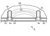
図1に示すように基台22において前記冷却機構3の奥側には偏平な円筒状の断熱体である熱板サポート部材5が埋め込まれている。図6,7に示すように熱板サポート部材5の底壁部分の内部及び側壁部分の内部には真空領域である真空層50が設けられた真空断熱構造となっているが、例えば中央部には円形状に真空層50が設けられており、その周囲には例えば後述するガス供給管57、ガス抜き孔58及び孔5aを避けるように同心円状に真空層50が設けられた構造となっている。
As shown in FIG. 1, a hot
熱板サポート部材5の下面には熱板サポート部材5を筺体20の底面にて支持する例えば3本の支柱51が周方向に設けられている。熱板サポート部材5の内周にはリング状の支持部材52が設けられ、支持部材52の上部には例えば耐熱樹脂やセラミックにより構成される断熱リング52aを介して円板状の熱板53が設けられている。熱板53はウエハW表面全体をカバーする大きさを有しており、また熱板サポート部材5の中に収まるように配置されている。
On the lower surface of the hot
熱板53の下面には図8で示すようなウエハWの加熱手段である、大きさの異なるリング状のヒータ53a〜53eが同心円状に設けられており、外側に位置しているヒータ53d及び53eは例えば周方向に4分割されている。また図示していないが熱板53の下面の例えば複数箇所に感温センサが設けられている。各ヒータ53a〜53eは電力供給部54に接続されており、後述の加熱装置2に備えられた制御部によって前記感温センサから制御部への出力に基づき当該電力供給部54を介して各ヒータ53a〜53eの発熱量が個別に制御される。このように構成されることにより熱板53は例えば加熱時に放熱性が高くなるウエハWの周縁部を中央部に比べて高い温度で加熱できる、つまり周縁部にオフセットをかけることができるように構成されている。ただしヒータの分割数(設置数)、形状、レイアウトはこの例に限られない。
On the lower surface of the
また熱板53上にはウエハWの裏面を支持する例えば4つの突起部55が熱板53の周方向に沿って設けられている。突起部55の高さとしては0.3〜1.0mmが好ましくこの例では0.3mmに設定してある。0.3mmより低いとウエハWが反っていた場合、特に12インチサイズ以上のウエハWの場合熱板53に接触して位置ずれを起こすおそれがあり、また1.0mmよりも高くなると熱板41の熱が当該ウエハWに充分に伝わらず温度について良好な面内均一性を確保しづらくなる。熱板サポート部材5の中央部及び熱板53の中央部には夫々3つの孔5a、5bが周方向に穿孔されている。前記孔5aを貫通するように昇降部材である3本の支持ピン26aが設けられており、これらの支持ピン26aは熱板サポート部材5の下方において熱板53の下方投影領域(熱板の真下)に設けられた駆動部26に接続されている。この駆動部26を介して支持ピン26aが鉛直方向に昇降し、当該支持ピン26aは前記孔5bを介して熱板53上に突没自在に構成されている。支持ピン26aがウエハWの裏面を支持したまま下降すると前記突起部55上にウエハWが受け渡されるようになっている。なお図6中5cは支持ピン26aが垂直に突没するための筒状のガイドである。
On the
ところで支持部材51、断熱リング52、熱板53及び熱板サポート部材5により囲まれる領域をガス流通部5A(図6参照)とすると、熱板サポート部材5には例えば複数箇所に複数のガス供給管57の一端が貫通して前記ガス流通部5Aに開口している。ガス供給管57の他端は熱板53の冷却用気体であるクリーンなパージ用ガス例えば窒素ガスなどの不活性ガスが貯留されているガス供給源57aに接続されている。またガス流通部5Aと連通するガス抜き孔58が例えば熱板サポート部材5の複数箇所に穿孔されており、ガス供給管57を介してガス供給源57aからガス流通部5Aにパージ用ガスが供給されると当該パージ用ガスはヒータ53a〜53e及びヒータにより加温された熱板53の熱を奪い取りガス抜き孔58を介してガス流通部5Aの外部へと流通するようになっている。このパージ用ガスの流通は熱板53の温度を下げるために行われる。
By the way, if the region surrounded by the
ところで熱板サポート部材5は一体的に成形された構造とされていても複数箇所で分割された構造とされていてもよい。具体的に例えば前記ガス供給管57が貫通されている孔、ガス抜き孔58及び孔5aが熱板サポート部材5の中央に設けられ、熱板サポート部材5はそれらの孔を含んだ中央部と中央部以外の周縁部が別々に形成され互いに嵌合されているような構造であってもよい。また熱板サポート部材5は既述のような有底の筒状構造ではなく、側壁が設けられていない熱板53の底面をカバーするようなプレート構造であってもよい。
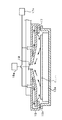
By the way, the hot
熱板サポート部材5の上端部には例えば4本の支柱61が間隔をおいて設けられ、支柱61の上部には例えば円形状に形成された天板6の周縁部が接続されている。天板6はウエハWの被加熱処理領域(半導体デバイス等の有効領域)をカバーする大きさ、この例では前記熱板53をカバーする大きさを有しており、熱板53と対向するように設けられている。熱板53と天板6との間隔は例えば12〜15mmとするのが好ましく、この加熱装置2においては14mmとしている。前記間隔がこの範囲よりも小さいと冷却プレート33が移動する際に天板6または熱板53に干渉するおそれがあり、この範囲よりも大きいとウエハWの加熱時に天板6の下面が充分に加熱されないおそれがある。
For example, four
天板6の中央下部には吸引排気口62が下に向かうほど拡径して開口しており、この吸引排気口62は天板6の上部に接続された排気ダクト63と連通している。この排気ダクト63の下流には前記局所排気ダクト24の端部が接続されており、さらにその下流には強制排気手段であるファン64が介設されている。また排気ダクト63の端部は、例えば工場の排気路に接続されている。前記ファン64の回転数が制御されることで例えば予め設定された排気量で吸引排気口62を介して天板6の周囲の排気が行われ、図9中矢印で示すように熱板53に載置されたウエハWの外周から中央に向かう気流を形成できるように天板6は構成されている。天板6の内部には吸引排気口62の周囲から天板6の端部へ向けて広がる真空層65が形成されており、当該天板6は真空断熱構造となっている。このような構造とすることで天板6はウエハWの加熱時に天板6の下面の温度がウエハWの加熱温度に近い温度で追従するように構成され、この加熱装置2においてはウエハWを加熱する際に熱板53の熱輻射を受けて前記天板6の下面の温度がウエハWの加熱温度の70%以上の温度に保たれるように構成されている。この加熱装置2のように熱板53と天板6との間隔が14mmである場合、天板6の下面の温度が例えば70%以下の温度になると、ウエハWの上面を通過する前記気流が冷却されて乱流となるおそれがあるため好ましくない。なお「ウエハWの加熱温度」とは、ウエハWの加熱処理時のウエハの温度である。
The
続いて加熱装置2に備えられた制御部について説明する。この制御部は、例えばコンピュータからなるプログラム格納部を有しており、プログラム格納部には後述するような加熱装置2の作用、つまりウエハWの処理、ウエハWの受け渡し、ウエハWの加熱及び気流の制御などが実施されるように命令が組まれた例えばソフトウエアからなるプログラムが格納される。そして当該プログラムが制御部に読み出されることにより制御部は後述する加熱装置2の作用を制御する。なおこのプログラムは、例えばハードディスク、コンパクトディスク、マグネットオプティカルディスク、メモリーカードなどの記録媒体に収納された状態でプログラム格納部に格納される。
Next, the control unit provided in the
次に加熱装置2の作用について説明する。既述の搬送アーム41を有するウエハWの搬送機構により、表面にレジスト液が塗布されたウエハWが搬送口21を介して筺体20内に搬入され、既述のようにウエハWは冷却プレート33に受け渡されると搬送アーム41は筺体20内から退去する。一方冷却機構3が熱板53に向けて移動するまでに熱板53の表面はヒータ53a〜53eにより予め設定された温度例えば130℃に加熱され、熱板53の熱輻射により天板6の下面が加熱される。
Next, the operation of the
ウエハWを保持した冷却プレート33が熱板53上に移動すると、支持ピン26aが上昇して冷却プレート33に載置されたウエハWの裏面を支持する。冷却機構3がホーム位置(図1の左端位置)に後退すると支持ピン26aは下降し、熱板53の突起部55上にウエハWが受け渡されウエハWが加熱される。この加熱時には必要に応じて前記ヒータ53a〜53eにおいて熱板53の外周側に設けられたヒータの発熱量は内周側に設けられたヒータの発熱量よりも大きくなるように調整される。
また加熱時にはファン64が回転することにより吸引排気口62から吸引排気が行われており、このため天板6と熱板53との間から外気(ここでは筺体20内の気体)が流入し、天板6と熱板53とにより気流が規制整流されることで既述のようにウエハWの外周から中央に向かう気流が形成される。このためウエハWに塗布されたレジスト液は熱板53の熱により溶剤が蒸発すると共にレジスト成分の一部が昇華し、これら溶剤蒸気と昇華成分とが前記気流に乗って吸引排気口62に吸い込まれ、こうしてレジスト液の乾燥が行われて、ウエハWにレジスト膜が形成される。
When the cooling
In addition, when the
例えば予め設定された時間ウエハWの加熱が行われた後に、支持ピン26aが上昇してウエハWを支持する。冷却プレート33がホーム位置から再び熱板53上へ移動して、ウエハWは冷却プレート33上に受け渡される。ウエハWの熱は冷却プレート33に伝熱され、冷却プレート33は蓄熱されて昇温するが、ホーム位置に戻ったときに、既述のように局所排気ダクト24の先端開口部と冷却機構3の下部側の空冷フィン部35とが一列に並んで局所排気ダクト24の吸引排気により空冷フィン部35内に気体が流通して当該空冷フィン部35が冷やされ、このため連結ブラケット31も冷却されてヒートパイプ38を介して冷却プレート33が冷却される。そしてウエハWの搬送機構が後述のように搬送スケジュールに従って当該ウエハWを取りにくるが、このときまでに冷却プレート33によってウエハWの粗熱取りが行われることになる。
For example, after the wafer W is heated for a preset time, the support pins 26a rise to support the wafer W. The cooling
前記搬送アーム41を備えた搬送機構は冷却プレート33上のウエハWを下方からすくい上げるようにして受け取り、当該ウエハWを筺体20の外へ搬送する。然る後、搬送機構によって後続のウエハWがこの加熱装置2に搬送されるがこの後続のウエハWにも同様に加熱処理が行われる。
なお例えばウエハWのロットが切り替わり、新たに加熱装置2に搬送されるウエハWの加熱温度が、今まで加熱装置2により処理されたウエハWの加熱温度よりも低い温度に切り替わる場合は、既述のようにガス供給管57を介してガス供給源57aからガス流通部5Aにパージ用ガスが供給され、このパージ用ガスにより熱板53が急冷されることで熱板53の温度が新たに搬送されるウエハWの加熱温度に従い調整される。
The transfer mechanism including the
For example, when the lot of the wafer W is switched and the heating temperature of the wafer W newly transferred to the
既述の加熱装置2によればレジスト液が塗布されたウエハWを、熱板53に載置して、天板6の中央部の下面に開口した吸引排気口62を介して天板6と熱板53との間の隙間から流入し、ウエハWと天板6との間をウエハWの外周から中央に向かう気流を形成しながら加熱するにあたって、内部に真空層65が設けられた天板6を用いているため熱板53側からの熱が逃げにくく、このため天板6と熱板53との間の周囲を開放したままにしても天板6の下面の温度をウエハWの温度に近付けることができる。従って天板6と熱板53との間を加熱処理時に密閉にするために天板6を昇降させる機構が不要になるし、あるいは天板6の下面の温度を高温にするためにヒータを付設するといった構成を採用しなくて済み、簡単な構造でありながらウエハWと天板6の下面との温度差が広がることが抑えられ、その結果として前記気流が冷却されることにより乱流となることを防ぐことができる。従ってウエハWに対して面内均一性の高い加熱処理を行うことができる。また天板6は簡単な構造を有するとともに、天板6の下面を高温化させて前記乱流の発生を防ぐことができるためウエハWの加熱処理時にウエハWに塗布されたレジスト液から発生する昇華物の天板6への付着が抑えられる結果、天板6のメンテナンスを容易に行うことができ、従って加熱装置2のメンテナンス時間の短縮を図ることができる。
さらにまた、ウエハWのロットが変わると処理温度が変わる場合が多いが天板6にヒータを設けない構成とすることで、一の処理温度から他の処理温度に下げる場合に、天板6の下面の温度が速やかにウエハWの温度に追従することから速やかにロットの切り替えを行うことができる。その他に天板6にヒータを設けない構成とすることで天板6の厚さを薄くすることができ、その結果として加熱装置2全体の省スペース化を図ることができる。
According to the
Furthermore, when the lot of wafers W changes, the processing temperature often changes. However, when the
また加熱装置2においては前記熱板53の下面側を覆うように内部に真空層50を備えた真空断熱材である断熱サポート部材5が設けられていることから、断熱サポート部材5の下方への熱板53の熱放散が抑えられるため、当該断熱サポート部材5を介して熱板53の下方投影領域内に支持ピン26aを昇降させるための駆動部26を設けるにあたって当該駆動部26の熱による劣化を抑えることができる。また駆動部26を熱板53の下方に設けることで駆動部26を熱板53の側方に設ける場合に比べて加熱装置2の占有床面積を抑えることができるため、加熱装置2の小型化を図ることができる。
Moreover, in the
さらに加熱装置2は、熱板53と熱板53の下面に設けられた断熱サポート部材5とにより囲まれるガス流通部5Aにガス供給源57aからガス供給管57を介してパージ用ガスが供給されることから、熱板53を急速に冷却することができ、熱板53が冷却されると天板6への熱放散が減少して、天板6の下面の温度が冷却された熱板53の温度に追従するように低下する。その結果として既述したようにウエハWのロットが切り替わり、新たに加熱装置2に搬送されるウエハWの加熱温度が今までの処理を受けたウエハWの加熱温度よりも低い温度に切り替わるような場合においてさらに速やかにロットの切り替えを行うことができ、また天板6及び熱板53の残余熱によりウエハWに対して過剰な加熱が行われることが抑えられることで高精度な加熱処理を行うことができる。
Further, in the
なお本発明の加熱装置は既述の実施形態のように天板の中央部から排気を行うものに限らず、例えば図10〜12に示すような構成であってもよい。これらの図に示した加熱装置7について説明する。この加熱装置7は、ウエハWを加熱する際の気流の形成方法については前記加熱装置2と大きく異なっている。図中70、71、72は夫々筺体、搬送口、基台である。図中73は冷却プレートであり、この冷却プレート73を含む冷却構造は既述の実施形態と同様の構造であってもよいがここでは例えば裏面に設けられた通路(不図示)を冷却水が流通することで載置されたウエハWを冷却する構成を示してある。74aは昇降機構74を介してウエハWの搬送機構と冷却プレート73との間でウエハWの受け渡しを行う支持ピンである。また75aは昇降機構75を介して冷却プレート73と熱板81との間でウエハWの受け渡しを行う支持ピンである。
熱板81は既述の熱板53と同様に構成され、またこの熱板81の側部及び底部は前記熱板サポート部材5と同様に構成された熱板サポート部材82に囲まれている。
なお図中81aは熱板上に設けられたウエハWが載置される突起部であり、図中82aはこの熱板サポート部材82の底壁部分の内部及び側壁部分の内部に設けられた真空領域である真空層である。図中83は支持部84を介して熱板81上に固定され、当該熱板81に載置されるウエハWと対向するように設けられた整流用の天板であり、この天板83の内部には例えば熱板81の表面をカバーする大きさを有する真空領域である真空層83aを備えている。また前記支持部84も内部に真空層84aを備えており、天板83及び支持部84は真空断熱構造となっている。
In addition, the heating apparatus of this invention is not restricted to what exhausts from the center part of a top plate like the above-mentioned embodiment, For example, a structure as shown to FIGS. The
The
In the figure, 81a is a protrusion on which a wafer W provided on a hot plate is placed, and 82a in the figure is a vacuum provided inside the bottom wall portion and the side wall portion of the hot
図中85は幅方向(図中Y方向)に沿って設けられたガス吐出部であり、熱板81を挟んでこのガス吐出部85と対向するように排気部86が設けられている。ガス吐出部85はウエハWの幅をカバーするように幅方向に沿って多数の小孔からなるクリーンなパージ用ガスを吐出するガス吐出口85aを備えており、排気部86にはガス吐出口85aと並行するように多数の小孔からなるガス排気口86aが設けられている。この加熱装置7は、ウエハWが熱板81の突起部81a上に載置され加熱される際にガス吐出口85aから天板83の下面に向けてパージ用ガスが吐出される一方でガス排気口86aから排気が行われ、図13に矢印で示すようにウエハWの幅をカバーし、ウエハWの一端側から多端側へ向かって流れる一方向流ともいうべき気流が形成されるように構成されている。
In the drawing,
このように加熱装置を構成した場合もウエハWの加熱時に天板の83の下面が加熱されることでウエハWの天板83とウエハWの表面との間における温度と、熱板81とウエハWの裏面との間における温度との差が広がることが抑えられ、前記一方向流が乱流となることが防がれる結果として面内均一性の高い加熱処理を行うことができる。
なおこのような一方向流を形成する方法としては、ガス吐出口85aを設けなくとも、天板6と熱板53との間の領域88において冷却プレート73が進入する側以外の3方を囲んで風洞を形成し、ガス排気口86aから排気することで冷却プレート73の進入口から気体を吸い込み一方向流を形成してもよい。
Even when the heating apparatus is configured in this way, the temperature between the
In addition, as a method for forming such a one-way flow, three regions other than the side where the cooling
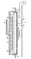
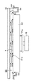
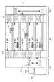
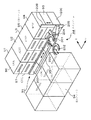
続いて既述した加熱装置2を塗布、現像装置に適用した場合の一実施の形態について説明する。図14は、レジストパターン形成装置の平面図を示し、図15は同概略斜視図、図16は同概略側面図である。この装置は、基板であるウエハWが例えば13枚密閉収納されたキャリア90を搬入出するためのキャリアブロックS1と、複数個例えば5個の単位ブロックB1〜B5を縦に配列して構成された処理ブロックS2と、インターフェイスブロックS3と、露光装置S4と、を備えている。
Next, an embodiment in which the
前記キャリアブロックS1には、前記キャリア90を複数個載置可能な載置台91と、この載置台91から見て前方の壁面に設けられる開閉部92と、開閉部92を介してキャリア90からウエハWを取り出すためのトランスファーアームCとが設けられている。このトランスファーアームCは、後述する単位ブロックB1、B2の受け渡しステージTRS1、TRS2との間でウエハWの受け渡しを行うように、進退自在、昇降自在、鉛直軸周りに回転自在、キャリア90の配列方向に移動自在に構成されている。
The carrier block S1 has a mounting table 91 on which a plurality of the
前記キャリアブロックS1の奥側には、筐体93にて周囲を囲まれる処理ブロックS2が接続されている。処理ブロックS2は、この例では、下方側から下段側の2段が現像処理を行うための第1及び第2の単位ブロック(DEV層)B1、B2、レジスト膜の上層側に形成される反射防止膜の形成処理を行うための第3の単位ブロック(TCT層)B3、レジスト液の塗布処理を行うための第4の単位ブロック(COT層)B4、レジスト膜の下層側に形成される反射防止膜の形成処理を行うための第5の単位ブロック(BCT層)B5として割り当てられている。ここで前記DEV層B1、B2が現像処理用の単位ブロック、TCT層B3、COT層B4、BCT層B5が塗布膜形成用の単位ブロックに相当する。
A processing block S2 surrounded by a
続いて、第1〜第5の単位ブロックB(B1〜B5)の構成について説明する。これら各単位ブロックB1〜B5は、ウエハWに対して薬液を塗布するための液処理ユニットと、前記液処理ユニットにて行われる処理の前処理及び後処理を行うための各種加熱・冷却系の処理ユニットと、これらの装置の加熱・冷却系の処理ユニットとの間でウエハWの受け渡しを行うための専用の搬送手段であるメインアームA1〜A5と、を備えている。 Next, the configuration of the first to fifth unit blocks B (B1 to B5) will be described. Each of these unit blocks B1 to B5 includes a liquid processing unit for applying a chemical solution to the wafer W, and various heating / cooling systems for performing pre-processing and post-processing of processing performed in the liquid processing unit. Main arms A1 to A5, which are dedicated transfer means for transferring the wafer W between the processing unit and the heating / cooling processing unit of these apparatuses, are provided.
先ず図14に示すCOT層B4を例にして以下に説明する。このCOT層B4のほぼ中央には、COT層B4の長さ方向(図中Y軸方向)に、キャリアブロックS1とインターフェイスブロックS3とを接続するための、ウエハWの搬送領域R1が形成されている。 First, the COT layer B4 shown in FIG. 14 will be described below as an example. Near the center of the COT layer B4, a transfer region R1 for the wafer W for connecting the carrier block S1 and the interface block S3 is formed in the length direction of the COT layer B4 (Y-axis direction in the figure). Yes.
この搬送領域R1のキャリアブロックS1側から見た両側には、手前側(キャリアブロックS1側)から奥側に向かって右側に、ウエハWにレジストの塗布処理を行うための複数個の塗布部を備えた塗布ユニット94が設けられている。またCOT層B4の手前側から奥側に向かって左側には、順に加熱・冷却系のユニットを多段化した4個の棚ユニットU1,U2,U3,U4が設けられており、塗布ユニット94にて行なわれる処理の前処理及び後処理を行うための各種ユニットを複数段、例えば2段に積層した構成とされている。
On both sides of the transfer region R1 as viewed from the carrier block S1 side, a plurality of coating units for performing resist coating processing on the wafer W are provided on the right side from the near side (carrier block S1 side) to the back side. A
上述の前処理及び後処理を行うための各種ユニットの中には、例えばレジスト液の塗布前にウエハWを所定の温度に調整するための冷却ユニット(COL)、レジスト液の塗布後にウエハWの加熱処理を行うための例えばプリベーキングユニットなどと呼ばれている加熱ユニット(CHP)95、ウエハWのエッジ部のみを選択的に露光するための周縁露光装置(WEE)等が含まれている。この例では図1〜図9で説明した加熱装置2はこの加熱ユニット95に相当する。また冷却ユニット(COL)や加熱ユニット(CHP)95等の各処理ユニットは、夫々処理容器96内に収納されており、棚ユニットU1〜U4は、前記処理容器96が2段に積層されて構成され、各処理容器96の搬送領域R1に臨む面にはウエハWを搬入出する搬送口97が形成されている。この例では加熱ユニット(CHP)95は棚ユニットU3として積層され、また棚ユニットU4に含まれている。
Among the various units for performing the above pre-processing and post-processing, for example, a cooling unit (COL) for adjusting the wafer W to a predetermined temperature before application of the resist solution, and the wafer W after application of the resist solution. For example, a heating unit (CHP) 95 called a pre-baking unit for performing the heat treatment, a peripheral exposure apparatus (WEE) for selectively exposing only the edge portion of the wafer W, and the like are included. In this example, the
前記搬送領域R1には前記メインアームA4が設けられている。このメインアームA4は、当該COT層B4内の全てのモジュール(ウエハWが置かれる場所)、例えば棚ユニットU1〜U4の各処理ユニット、塗布ユニット94、後述する棚ユニットU5と棚ユニットU6の各部との間でウエハの受け渡しを行うように構成されており、このために進退自在、昇降自在、鉛直軸回りに回転自在、Y軸方向に移動自在に構成されている。
The main arm A4 is provided in the transfer region R1. The main arm A4 includes all modules (places where the wafer W is placed) in the COT layer B4, for example, each processing unit of the shelf units U1 to U4, a
また搬送領域R1のキャリアブロックS1と隣接する領域は、第1のウエハ受け渡し領域R2となっていて、この領域R2には、図14及び図16に示すように、トランスファーアームCとメインアームA4とがアクセスできる位置に棚ユニットU5が設けられると共に、この棚ユニットU5に対してウエハWの受け渡しを行うための第1の基板受け渡し手段をなす第1の受け渡しアームD1を備えている。 An area adjacent to the carrier block S1 in the transfer area R1 is a first wafer transfer area R2, which includes a transfer arm C, a main arm A4, and a transfer arm C, as shown in FIGS. A shelf unit U5 is provided at a position accessible by the first unit, and a first transfer arm D1 serving as a first substrate transfer unit for transferring the wafer W to the shelf unit U5 is provided.
前記棚ユニットU5は、図16に示すように、各単位ブロックB1〜B5のメインアームA1〜A5との間でウエハWの受け渡しを行うように、この例では各単位ブロックB1〜B5は、1個以上例えば2個の第1の受け渡しステージTRS1〜TRS5を備えており、これにより第1の受け渡しステージが多段に積層された第1の受け渡しステージ群を構成している。また第1の受け渡しアームD1は各第1の受け渡しステージTRS1〜TRS5に対してウエハWの受け渡しを行うことができるように、進退自在及び昇降自在に構成されている。また前記第1及び第2の単位ブロックB1、B2の第1の受け渡しステージTRS1、TRS2は、この例ではトランスファーアームCとの間でウエハWの受け渡しが行なわれるように構成され、キャリアブロック用受け渡しステージに相当する。 As shown in FIG. 16, the shelf unit U5 transfers wafers W to and from the main arms A1 to A5 of the unit blocks B1 to B5. In this example, each of the unit blocks B1 to B5 is 1 More than two, for example, two first delivery stages TRS1 to TRS5 are provided, thereby constituting a first delivery stage group in which the first delivery stages are stacked in multiple stages. Further, the first delivery arm D1 is configured to be movable forward and backward and up and down so that the wafer W can be delivered to the first delivery stages TRS1 to TRS5. In this example, the first transfer stages TRS1 and TRS2 of the first and second unit blocks B1 and B2 are configured to transfer the wafer W to and from the transfer arm C. Corresponds to the stage.
さらに搬送領域R1のインターフェイスブロックS3と隣接する領域は、第2のウエハ受け渡し領域R3となっていて、この領域R3には、図14に示すように、メインアームA4がアクセスできる位置に棚ユニットU6が設けられると共に、この棚ユニットU6に対してウエハWの受け渡しを行うための第2の基板受け渡し手段をなす第2の受け渡しアームD2を備えている。 Further, the area adjacent to the interface block S3 in the transfer area R1 is a second wafer transfer area R3. As shown in FIG. 14, the shelf unit U6 is located at a position accessible by the main arm A4. And a second transfer arm D2 which forms a second substrate transfer means for transferring the wafer W to the shelf unit U6.
前記棚ユニットU6は、図16に示すように、各単位ブロックB1〜B5のメインアームA1〜A5との間でウエハWの受け渡しを行うように、この例では各単位ブロックB1〜B5は、1個以上例えば2個の第2の受け渡しステージTRS6〜TRS10を備えており、これにより第2の受け渡しステージが多段に積層された第2の受け渡しステージ群が構成されている。第2の受け渡しアームD2は各第2の受け渡しステージTRS6〜TRS10に対してウエハWの受け渡しを行うことができるように、進退自在及び昇降自在に構成されている。このように本実施の形態では、5段に積層された各単位ブロックB1〜B5の間で、上述の第1の受け渡しアームD1と第2の受け渡しアームD2とにより、夫々第1の受け渡しステージTRS1〜TRS5、第2の受け渡しステージTRS6〜TRS10を介して、自由にウエハWの受け渡しを行なうことができるように構成されている。 As shown in FIG. 16, the shelf unit U6 transfers wafers W to and from the main arms A1 to A5 of the unit blocks B1 to B5. In this example, each of the unit blocks B1 to B5 is 1 More than two, for example, two second delivery stages TRS6 to TRS10 are provided, and thereby a second delivery stage group in which the second delivery stages are stacked in multiple stages is configured. The second delivery arm D2 is configured to be movable forward and backward and up and down so that the wafer W can be delivered to the second delivery stages TRS6 to TRS10. As described above, in the present embodiment, the first delivery stage TRS1 is respectively provided between the unit blocks B1 to B5 stacked in five stages by the first delivery arm D1 and the second delivery arm D2. Through the TRS5 and the second delivery stages TRS6 through TRS10, the wafer W can be freely delivered.
続いて他の単位ブロックBについて簡単に説明する。DEV層B1、B2は同様に構成され、ウエハWに対して現像処理を行うための複数個の現像部を備えた現像ユニットが設けられ、棚ユニットU1〜U4には、露光後のウエハWを加熱処理するポストエクスポージャーベーキングユニットなどと呼ばれている加熱ユニット(PEB)や、この加熱ユニット(PEB)における処理の後にウエハWを所定温度に調整するための冷却ユニット(COL)、現像処理後のウエハWを水分を飛ばすために加熱処理するポストベーキングユニットなどと呼ばれている加熱ユニット(POST)を備えている以外はCOT層B4と同様に構成されている。なおDEV層B1、B2に設けられたこれらの加熱ユニットはCOT層B4に設けられた加熱ユニット95と例えば同じ構成を有し、処理温度及び処理時間のみが異なるものとする。
Next, another unit block B will be briefly described. The DEV layers B1 and B2 are configured in the same manner, and a development unit having a plurality of development units for performing development processing on the wafer W is provided. The shelf units U1 to U4 are provided with the wafer W after exposure. A heating unit (PEB) called a post-exposure baking unit for heating processing, a cooling unit (COL) for adjusting the wafer W to a predetermined temperature after processing in the heating unit (PEB), The wafer W is configured in the same manner as the COT layer B4 except that it includes a heating unit (POST) called a post-baking unit that heats the wafer W to remove moisture. These heating units provided in the DEV layers B1 and B2 have, for example, the same configuration as the
そしてこれらDEV層B1,B2では、夫々メインアームA1,A2により、夫々第1の受け渡しステージTRS1、TRS2、第2の受け渡しステージTRS6、TRS7と、現像ユニットと、棚ユニットU1〜U4の各処理ユニットとに対してウエハWの受け渡しが行われるようになっている。 In the DEV layers B1 and B2, the main arms A1 and A2 respectively use the first transfer stages TRS1 and TRS2, the second transfer stages TRS6 and TRS7, the developing units, and the processing units of the shelf units U1 to U4. The wafer W is transferred to and from the above.
またTCT層B3は、ウエハWに対して第2の反射防止膜の形成処理を行うための複数個の第2の反射防止膜形成部を備えた第2の反射防止膜形成ユニットが設けられている。即ち、第2の反射防止膜形成ユニットは、レジスト液を塗布した後にウエハWに反射防止膜用の薬液を塗布するための装置である。また薬液ノズル12aに形成された吐出口からは反射防止膜用の薬液が吐出されることになる。また棚ユニットU1〜U4は、反射防止膜形成処理前にウエハWを所定温度に調整するための冷却ユニット(COL)や、反射防止膜形成処理後のウエハWを加熱処理する加熱ユニット(CHP)が備えている以外はCOT層B4と同様に構成されている。なお前記加熱ユニット(CHP)はCOT層B4に設けられた加熱ユニット95と例えば同じ構成を有し、処理温度及び処理時間のみが異なるものとする。そしてこのTCT層B3では、メインアームA3により、第1の受け渡しステージTRS3、第2の受け渡しステージTRS8と、第2の反射防止膜形成ユニットと、棚ユニットU1〜U4の各処理ユニットとに対してウエハWの受け渡しが行われるようになっている。
Further, the TCT layer B3 is provided with a second antireflection film forming unit including a plurality of second antireflection film forming portions for performing a second antireflection film forming process on the wafer W. Yes. That is, the second antireflection film forming unit is an apparatus for applying a chemical solution for the antireflection film to the wafer W after applying the resist solution. Further, the chemical liquid for the antireflection film is discharged from the discharge port formed in the chemical
そしてBCT層B5は、ウエハWに対して第1の反射防止膜の形成処理を行うための複数個の第1の反射防止膜形成部を備えた第1の反射防止膜形成ユニットが設けられている。即ち、前記第1の反射防止膜形成ユニットは、レジスト液を塗布する前にウエハWに反射防止膜用の薬液を塗布するための装置である。また棚ユニットU1〜U4は、反射防止膜形成処理前にウエハWを所定温度に調整するための冷却ユニット(COL)や、反射防止膜形成処理後のウエハWを加熱処理する加熱ユニット(CHP)を備え、周縁露光装置(WEE)を備えていない以外はCOT層B4と同様に構成されている。なお前記加熱ユニット(CHP)はCOT層B4に設けられた加熱ユニット95と例えば同じ構成を有し、処理温度及び処理時間のみが異なるものとする。そしてこの第5の単位ブロックB5では、メインアームA5により、第1の受け渡しステージTRS5,第2の受け渡しステージTRS10と、第1の反射防止膜形成ユニットと、棚ユニットU1〜U4の各処理ユニットと、に対してウエハWの受け渡しが行われるようになっている。
The BCT layer B5 is provided with a first antireflection film forming unit including a plurality of first antireflection film forming portions for performing a first antireflection film forming process on the wafer W. Yes. That is, the first antireflection film forming unit is an apparatus for applying a chemical solution for the antireflection film to the wafer W before applying the resist solution. Further, the shelf units U1 to U4 are a cooling unit (COL) for adjusting the wafer W to a predetermined temperature before the antireflection film forming process, or a heating unit (CHP) for heating the wafer W after the antireflection film forming process. And is configured in the same manner as the COT layer B4 except that the peripheral edge exposure apparatus (WEE) is not provided. The heating unit (CHP) has, for example, the same configuration as the
なお、これら処理ユニットは加熱ユニット(CHP、PEB、POST)、冷却ユニット(COL)、周縁露光装置(WEE)に限らず、他の処理ユニットを設けるようにしてもよいし、実際の装置では各処理ユニットの処理時間などを考慮してユニットの設置数が決められる。 These processing units are not limited to the heating unit (CHP, PEB, POST), the cooling unit (COL), and the edge exposure apparatus (WEE), and other processing units may be provided. The number of units installed is determined in consideration of the processing time of the processing units.
一方、処理ブロックS2における棚ユニットU6の奥側には、インターフェイスブロックS3を介して露光装置S4が接続されている。インターフェイスブロックS3には、処理ブロックS2の棚ユニットU6と露光装置S4とに対してウエハWの受け渡しを行うためのインターフェイスアームBを備えている。このインターフェイスアームBは、処理ブロックS2と露光装置S4との間に介在するウエハWの搬送手段をなすものであり、この例では、第1〜第4の単位ブロックB1〜B4の第2の受け渡しステージTRS6〜TRS9に対してウエハWの受け渡しを行うように、進退自在、昇降自在、鉛直軸回りに回転自在に構成され、この例では第2の受け渡しステージTRS6〜TRS9がインターフェイスブロック用受け渡しステージに相当する。 On the other hand, an exposure apparatus S4 is connected to the back side of the shelf unit U6 in the processing block S2 via an interface block S3. The interface block S3 includes an interface arm B for delivering the wafer W to the shelf unit U6 of the processing block S2 and the exposure apparatus S4. The interface arm B serves as a transfer means for the wafer W interposed between the processing block S2 and the exposure apparatus S4. In this example, the second delivery of the first to fourth unit blocks B1 to B4 is performed. In order to transfer the wafer W to the stages TRS6 to TRS9, it is configured to be movable back and forth, vertically movable, and rotatable about the vertical axis. In this example, the second transfer stages TRS6 to TRS9 serve as interface block transfer stages. Equivalent to.
また前記インターフェイスアームBは、全ての単位ブロックB1〜B5の第2の受け渡しステージTRS6〜TRS10に対してウエハWの受け渡しを行うように構成してもよく、この場合には第2の受け渡しステージTRS6〜TRS10がインターフェイスブロック用受け渡しステージに相当する。 The interface arm B may be configured to transfer the wafer W to the second transfer stages TRS6 to TRS10 of all the unit blocks B1 to B5. In this case, the second transfer stage TRS6 is used. ˜TRS10 corresponds to the interface block transfer stage.
続いてメインアームA(A1〜A5)についてCOT層のメインアームA4を例にして簡単に説明すると、図17に示すようにメインアームA4は、ウエハWの裏面側周縁領域を支持するための2本の搬送アーム201、202を備えており、これら搬送アーム201、202は搬送基体203に沿って互いに独立して進退自在に構成されている。またこの搬送基体203は回転機構204により鉛直軸回りに回転自在に構成されると共に、移動機構205により、棚ユニットU1〜U4を支持する台部206の搬送領域R1に臨む面に取り付けられたY軸レール207に沿ってY軸方向に移動自在、且つ昇降レール208に沿って昇降自在に構成されている。こうして搬送アーム201、202は、進退自在、Y軸方向に移動自在、昇降自在、鉛直軸回りに回転自在に構成されている。メインアームA1〜A3及びA5もメインアームA4と同様に構成されており、メインアームAは、棚ユニットU1〜U6の各ユニットや第1及び第2の受け渡しステージTRS1〜TRS10、液処理ユニットとの間でウエハWの受け渡しを行うことができるようになっている。
Next, the main arm A (A1 to A5) will be briefly described by taking the main arm A4 of the COT layer as an example. The main arm A4 is a 2 for supporting the rear surface side peripheral region of the wafer W as shown in FIG. The
COT層B4では、ウエハWはメインアームA4により搬送口97を介して加熱ユニット内に搬送され、レジスト液が塗布された後にウエハWは搬送口97を介してメインアームA4により加熱ユニット95の外部に搬送される。
In the COT layer B4, the wafer W is transferred into the heating unit via the
ここでこのレジストパターン形成装置におけるウエハWの流れについて、レジスト膜の上下に夫々反射防止膜を形成する場合を例にして説明する。先ず外部からキャリア90がキャリアブロック91に搬入され、トランスファーアームCによりこのキャリア90内からウエハWが取り出される。ウエハWは、トランスファーアームCから、先ず第2の単位ブロックB2の棚ユニットU5の第1の受け渡しステージTRS2に受け渡され、次いでウエハWはBCT層B5にウエハWを受け渡すために、第1の受け渡しアームD1により第1の受け渡し部TRS5を介してBCT層B5のメインアームA5に受け渡される。そしてBCT層B5では、メインアームA5により、冷却ユニット(COL)→第1の反射防止膜形成ユニット→加熱ユニット(CHP)→棚ユニットU6の第2の受け渡しステージTRS10の順序で搬送されて、第1の反射防止膜が形成される。
Here, the flow of the wafer W in this resist pattern forming apparatus will be described by taking as an example the case where antireflection films are formed above and below the resist film, respectively. First, the
続いて第2の受け渡しステージTRS10のウエハWは第2の受け渡しアームD2により、COT層B4にウエハWを受け渡すために第2の受け渡しステージTRS9に搬送され、次いで当該COT層B4のメインアームA4に受け渡される。そしてCOT層B4では、メインアームA4により、冷却ユニット(COL)→塗布ユニット94→加熱ユニット(CHP)95→第1の受け渡しステージTRS4の順序で搬送されて、第1の反射防止膜の上にレジスト膜が形成される。
Subsequently, the wafer W of the second delivery stage TRS10 is transferred to the second delivery stage TRS9 in order to deliver the wafer W to the COT layer B4 by the second delivery arm D2, and then the main arm A4 of the COT layer B4. Is passed on. Then, in the COT layer B4, the main arm A4 transports the cooling unit (COL) → the
次いで受け渡しステージTRS4のウエハWは第1の受け渡しアームD1によ
り、TCT層B3にウエハWを受け渡すために第1の受け渡しステージTRS3に搬送され、当該TCT層B3のメインアームA3に受け渡される。そしてTCT層B3では、メインアームA3により、冷却ユニット(COL)→第2の反射防止膜形成ユニット→加熱ユニット(CHP)→周縁露光装置(WEE)→棚ユニットU6の第2の受け渡しステージTRS8の順序で搬送されて、レジスト膜の上に第2の反射防止膜が形成される。
Next, the wafer W of the transfer stage TRS4 is transferred to the first transfer stage TRS3 by the first transfer arm D1 to transfer the wafer W to the TCT layer B3, and transferred to the main arm A3 of the TCT layer B3. In the TCT layer B3, the main arm A3 causes the cooling unit (COL) → second antireflection film forming unit → heating unit (CHP) → periphery exposure apparatus (WEE) → second delivery stage TRS8 of the shelf unit U6. The second antireflection film is formed on the resist film by being conveyed in order.
続いて第2の受け渡しステージTRS8のウエハWはインターフェイスアームBにより露光装置S4に搬送され、ここで所定の露光処理が行われる。露光処理後のウエハWは、インターフェイスアームBにより、DEV層B1(DEV層B2)にウエハWを受け渡すために、棚ユニットU6の第2の受け渡しステージTRS6(TRS7)に搬送され、このステージTRS6(TRS7)上のウエハWは、DEV層B1(DEV層B2)メインアームA1(メインアームA2)に受け取られ、当該DEV層B1(B2)にて、先ず加熱ユニット(PEB)→冷却ユニット(COL)→現像ユニット→加熱ユニット(POST)の順序で搬送され、所定の現像処理が行われる。こうして現像処理が行われたウエハWは、トランスファーアームCにウエハWを受け渡すために、第1の受け渡しステージTRS1(TRS2)に搬送され、トランスファーアームCにより、キャリアブロックS1に載置されている元のキャリア90に戻される。
Subsequently, the wafer W on the second delivery stage TRS8 is transferred to the exposure apparatus S4 by the interface arm B, where a predetermined exposure process is performed. The wafer W after the exposure processing is transferred to the second transfer stage TRS6 (TRS7) of the shelf unit U6 in order to transfer the wafer W to the DEV layer B1 (DEV layer B2) by the interface arm B, and this stage TRS6. The wafer W on (TRS7) is received by the DEV layer B1 (DEV layer B2) main arm A1 (main arm A2), and in the DEV layer B1 (B2), first, the heating unit (PEB) → the cooling unit (COL). ) → development unit → heating unit (POST) in this order, and a predetermined development process is performed. The wafer W thus developed is transferred to the first transfer stage TRS1 (TRS2) to transfer the wafer W to the transfer arm C, and is placed on the carrier block S1 by the transfer arm C. Returned to the
このように本発明の加熱装置を塗布、現像装置に設けられる加熱ユニットとして適用することで、塗布膜形成用の各ブロックB3〜B5にて、塗布液としてレジスト液または反射防止膜用の薬液が塗布されたウエハWに対して、既述したように加熱時に天板6の内部に真空層65を設けることにより、加熱時に形成される気流が乱流となることが抑えられるので、面内均一性の高いウエハWの加熱処理を行うことができることから、当該ウエハWに良好なレジストパターンを形成することができる。
Thus, by applying the heating device of the present invention as a heating unit provided in the coating and developing device, a resist solution or an antireflection film chemical solution is applied as a coating solution in each of the coating film forming blocks B3 to B5. As described above, by providing the
なお加熱装置2は基板にレジスト膜を形成する塗布、現像装置以外にも例えば液体である絶縁膜の前駆体を基板に塗布して当該液体を加熱させることで基板に絶縁膜を形成する絶縁膜形成装置にも適用できる。
In addition to the coating and developing device for forming a resist film on the substrate, the
2 加熱装置
3 冷却機構
33 冷却プレート
5 熱板サポート部材
53 熱板
6 天板
50,65 真空層
2
Claims (2)
基板を収納しキャリアが搬入されるキャリアブロックと、
このキャリアブロックよりも奥側に設けられ、前記キャリアから取り出された露光前の基板の表面に塗布膜を形成するための塗布ブロックと、
この塗布ブロックの奥側に設けられ、当該処理ブロックと露光装置との間で基板の受け渡しを行うインターフェイス部と、を備え
前記塗布ブロックは、キャリアブロック側からインターフェイス部側に直線状に伸びる基板搬送路と、この基板搬送路の一方の側方に設けられ、レジスト液を塗布するための塗布部と、前記基板搬送路の他方の側方に設けられ、基板を加熱するための加熱装置と、前記基板搬送路に沿って基板を搬送し、前記塗布部と加熱装置との間で基板の受け渡しを行う基板搬送機構と、を備え、
前記加熱装置は、基板搬送路から見て奥側に配置され、基板を加熱する加熱プレートと、この加熱プレートよりも基板搬送路側に設けられ、基板を冷却する冷却プレートと、前加熱プレートと冷却プレートとの間で基板を搬送する専用の専用搬送機構と、を備えたことを特徴とする塗布、現像装置。 In a developing device for forming a resist film on a substrate and developing the exposed substrate,
A carrier block for storing a substrate and carrying a carrier;
A coating block for forming a coating film on the surface of the substrate before exposure, which is provided behind the carrier block and is taken out of the carrier,
An interface unit that is provided on the back side of the coating block and that transfers the substrate between the processing block and the exposure apparatus, and the coating block linearly extends from the carrier block side to the interface unit side. A path, one side of the substrate transport path, an application unit for applying a resist solution, a heating device provided on the other side of the substrate transport path, for heating the substrate, A substrate transport mechanism that transports the substrate along the substrate transport path and delivers the substrate between the coating unit and the heating device;
The heating device is disposed on the back side when viewed from the substrate conveyance path, and is provided with a heating plate for heating the substrate, a cooling plate for cooling the substrate, provided on the substrate conveyance path side with respect to the heating plate, a preheating plate, and a cooling plate A coating and developing apparatus, comprising: a dedicated transport mechanism for transporting a substrate to and from a plate.
Priority Applications (1)
| Application Number | Priority Date | Filing Date | Title |
|---|---|---|---|
| JP2009287783A JP5158066B2 (en) | 2009-12-18 | 2009-12-18 | Coating and developing equipment |
Applications Claiming Priority (1)
| Application Number | Priority Date | Filing Date | Title |
|---|---|---|---|
| JP2009287783A JP5158066B2 (en) | 2009-12-18 | 2009-12-18 | Coating and developing equipment |
Related Parent Applications (1)
| Application Number | Title | Priority Date | Filing Date |
|---|---|---|---|
| JP2005121267A Division JP4535499B2 (en) | 2005-04-19 | 2005-04-19 | Heating device, coating, developing device and heating method |
Publications (3)
| Publication Number | Publication Date |
|---|---|
| JP2010074185A true JP2010074185A (en) | 2010-04-02 |
| JP2010074185A5 JP2010074185A5 (en) | 2011-02-24 |
| JP5158066B2 JP5158066B2 (en) | 2013-03-06 |
Family
ID=42205623
Family Applications (1)
| Application Number | Title | Priority Date | Filing Date |
|---|---|---|---|
| JP2009287783A Active JP5158066B2 (en) | 2009-12-18 | 2009-12-18 | Coating and developing equipment |
Country Status (1)
| Country | Link |
|---|---|
| JP (1) | JP5158066B2 (en) |
Cited By (2)
| Publication number | Priority date | Publication date | Assignee | Title |
|---|---|---|---|---|
| JP2013145916A (en) * | 2013-04-08 | 2013-07-25 | Tokyo Electron Ltd | Heat treatment apparatus, heat treatment method, and storage medium |
| JP2014022570A (en) * | 2012-07-18 | 2014-02-03 | Sokudo Co Ltd | Substrate processing apparatus and substrate processing method |
Citations (12)
| Publication number | Priority date | Publication date | Assignee | Title |
|---|---|---|---|---|
| JP2000150616A (en) * | 1998-11-18 | 2000-05-30 | Matsushita Electric Ind Co Ltd | Plasma cleaning device for substrate |
| JP2000312463A (en) * | 1999-04-27 | 2000-11-07 | Shinko Electric Co Ltd | Splicing structure of rail for linear motor |
| JP2001117064A (en) * | 1999-10-19 | 2001-04-27 | Tokyo Electron Ltd | Alignment mechanism and alignment method for transporting device as well as substrate treating device |
| JP2001176792A (en) * | 1999-12-06 | 2001-06-29 | Dns Korea Co Ltd | Lithography system in semiconductor manufacturing |
| JP2002057200A (en) * | 2000-08-09 | 2002-02-22 | Tokyo Electron Ltd | Conveying method for wafer |
| JP2003285902A (en) * | 2002-03-29 | 2003-10-07 | Murata Mach Ltd | Carrying installation |
| JP2004128249A (en) * | 2002-10-03 | 2004-04-22 | Sendai Nikon:Kk | Substrate holding and carrying method, device therefor, substrate holder, substrate carrying device, and aligner |
| JP2004146450A (en) * | 2002-10-22 | 2004-05-20 | Tokyo Electron Ltd | Substrate processing apparatus |
| JP2004214696A (en) * | 1999-10-19 | 2004-07-29 | Tokyo Electron Ltd | Apparatus and method for treating substrate |
| JP2004235659A (en) * | 2004-03-15 | 2004-08-19 | Tokyo Electron Ltd | Block for processing substrate and device for processing substrate |
| JP2005011853A (en) * | 2003-06-16 | 2005-01-13 | Tokyo Electron Ltd | Method of aligning substrate treatment apparatus with substrate transfer means |
| JP2005064242A (en) * | 2003-08-12 | 2005-03-10 | Tokyo Electron Ltd | Processing system of substrate and heat-treatment method of substrate |
-
2009
- 2009-12-18 JP JP2009287783A patent/JP5158066B2/en active Active
Patent Citations (12)
| Publication number | Priority date | Publication date | Assignee | Title |
|---|---|---|---|---|
| JP2000150616A (en) * | 1998-11-18 | 2000-05-30 | Matsushita Electric Ind Co Ltd | Plasma cleaning device for substrate |
| JP2000312463A (en) * | 1999-04-27 | 2000-11-07 | Shinko Electric Co Ltd | Splicing structure of rail for linear motor |
| JP2001117064A (en) * | 1999-10-19 | 2001-04-27 | Tokyo Electron Ltd | Alignment mechanism and alignment method for transporting device as well as substrate treating device |
| JP2004214696A (en) * | 1999-10-19 | 2004-07-29 | Tokyo Electron Ltd | Apparatus and method for treating substrate |
| JP2001176792A (en) * | 1999-12-06 | 2001-06-29 | Dns Korea Co Ltd | Lithography system in semiconductor manufacturing |
| JP2002057200A (en) * | 2000-08-09 | 2002-02-22 | Tokyo Electron Ltd | Conveying method for wafer |
| JP2003285902A (en) * | 2002-03-29 | 2003-10-07 | Murata Mach Ltd | Carrying installation |
| JP2004128249A (en) * | 2002-10-03 | 2004-04-22 | Sendai Nikon:Kk | Substrate holding and carrying method, device therefor, substrate holder, substrate carrying device, and aligner |
| JP2004146450A (en) * | 2002-10-22 | 2004-05-20 | Tokyo Electron Ltd | Substrate processing apparatus |
| JP2005011853A (en) * | 2003-06-16 | 2005-01-13 | Tokyo Electron Ltd | Method of aligning substrate treatment apparatus with substrate transfer means |
| JP2005064242A (en) * | 2003-08-12 | 2005-03-10 | Tokyo Electron Ltd | Processing system of substrate and heat-treatment method of substrate |
| JP2004235659A (en) * | 2004-03-15 | 2004-08-19 | Tokyo Electron Ltd | Block for processing substrate and device for processing substrate |
Cited By (4)
| Publication number | Priority date | Publication date | Assignee | Title |
|---|---|---|---|---|
| JP2014022570A (en) * | 2012-07-18 | 2014-02-03 | Sokudo Co Ltd | Substrate processing apparatus and substrate processing method |
| US9828676B2 (en) | 2012-07-18 | 2017-11-28 | Screen Semiconductor Solutions Co., Ltd. | Substrate processing apparatus and substrate processing method |
| US10047441B2 (en) | 2012-07-18 | 2018-08-14 | Screen Semiconductor Solutions Co., Ltd. | Substrate processing apparatus and substrate processing method |
| JP2013145916A (en) * | 2013-04-08 | 2013-07-25 | Tokyo Electron Ltd | Heat treatment apparatus, heat treatment method, and storage medium |
Also Published As
| Publication number | Publication date |
|---|---|
| JP5158066B2 (en) | 2013-03-06 |
Similar Documents
| Publication | Publication Date | Title |
|---|---|---|
| JP4535499B2 (en) | Heating device, coating, developing device and heating method | |
| JP4410147B2 (en) | Heating device, coating, developing device and heating method | |
| JP4606355B2 (en) | Heat treatment apparatus, heat treatment method and storage medium | |
| KR101059309B1 (en) | Heating device, coating, developing device and heating method | |
| TWI326805B (en) | Coating and developing apparatus and coating and developing method | |
| JP4450784B2 (en) | Coating and developing apparatus and method thereof | |
| TWI425586B (en) | Substrate transport apparatus and heat treatment apparatus | |
| JP2006229184A (en) | Coating, developing device and method | |
| KR20070026198A (en) | Heating apparatus and coating,developing apparatus | |
| JP2010182906A (en) | Substrate treatment apparatus | |
| JP4737083B2 (en) | Heating device, coating, developing device and heating method | |
| JP3180048U (en) | Heat treatment equipment | |
| JP4765750B2 (en) | Heat treatment apparatus, heat treatment method, storage medium | |
| JP3898895B2 (en) | Heat treatment apparatus and heat treatment method | |
| JP5158066B2 (en) | Coating and developing equipment | |
| JP2007234980A (en) | Heat treatment apparatus | |
| JP4827263B2 (en) | Heat treatment equipment | |
| JP2010074185A5 (en) | ||
| JP2001237157A (en) | Heat treatment device | |
| JP2007067111A (en) | Heater, coater, developer, and heating method | |
| JP2002203779A (en) | Heat treatment equipment | |
| JP4800226B2 (en) | Heat treatment equipment | |
| JP2005159377A (en) | Heat treatment apparatus | |
| JP3982672B2 (en) | Heat treatment apparatus and heat treatment method | |
| JPH11238674A (en) | Heat-treatment device |
Legal Events
| Date | Code | Title | Description |
|---|---|---|---|
| A621 | Written request for application examination |
Free format text: JAPANESE INTERMEDIATE CODE: A621 Effective date: 20091224 |
|
| A521 | Request for written amendment filed |
Free format text: JAPANESE INTERMEDIATE CODE: A523 Effective date: 20100511 |
|
| A521 | Request for written amendment filed |
Free format text: JAPANESE INTERMEDIATE CODE: A523 Effective date: 20100531 |
|
| A521 | Request for written amendment filed |
Free format text: JAPANESE INTERMEDIATE CODE: A523 Effective date: 20101228 |
|
| A131 | Notification of reasons for refusal |
Free format text: JAPANESE INTERMEDIATE CODE: A131 Effective date: 20111108 |
|
| A521 | Request for written amendment filed |
Free format text: JAPANESE INTERMEDIATE CODE: A523 Effective date: 20120110 |
|
| A131 | Notification of reasons for refusal |
Free format text: JAPANESE INTERMEDIATE CODE: A131 Effective date: 20120724 |
|
| A521 | Request for written amendment filed |
Free format text: JAPANESE INTERMEDIATE CODE: A523 Effective date: 20120924 |
|
| TRDD | Decision of grant or rejection written | ||
| A01 | Written decision to grant a patent or to grant a registration (utility model) |
Free format text: JAPANESE INTERMEDIATE CODE: A01 Effective date: 20121113 |
|
| A61 | First payment of annual fees (during grant procedure) |
Free format text: JAPANESE INTERMEDIATE CODE: A61 Effective date: 20121126 |
|
| R150 | Certificate of patent or registration of utility model |
Ref document number: 5158066 Country of ref document: JP Free format text: JAPANESE INTERMEDIATE CODE: R150 Free format text: JAPANESE INTERMEDIATE CODE: R150 |
|
| FPAY | Renewal fee payment (event date is renewal date of database) |
Free format text: PAYMENT UNTIL: 20151221 Year of fee payment: 3 |
|
| R250 | Receipt of annual fees |
Free format text: JAPANESE INTERMEDIATE CODE: R250 |
|
| R250 | Receipt of annual fees |
Free format text: JAPANESE INTERMEDIATE CODE: R250 |
|
| R250 | Receipt of annual fees |
Free format text: JAPANESE INTERMEDIATE CODE: R250 |
|
| R250 | Receipt of annual fees |
Free format text: JAPANESE INTERMEDIATE CODE: R250 |
|
| R250 | Receipt of annual fees |
Free format text: JAPANESE INTERMEDIATE CODE: R250 |
|
| R250 | Receipt of annual fees |
Free format text: JAPANESE INTERMEDIATE CODE: R250 |
|
| R250 | Receipt of annual fees |
Free format text: JAPANESE INTERMEDIATE CODE: R250 |