JP2010072401A - 光導波装置 - Google Patents
光導波装置 Download PDFInfo
- Publication number
- JP2010072401A JP2010072401A JP2008240526A JP2008240526A JP2010072401A JP 2010072401 A JP2010072401 A JP 2010072401A JP 2008240526 A JP2008240526 A JP 2008240526A JP 2008240526 A JP2008240526 A JP 2008240526A JP 2010072401 A JP2010072401 A JP 2010072401A
- Authority
- JP
- Japan
- Prior art keywords
- waveguide
- mesa
- high mesa
- substrate
- buried
- Prior art date
- Legal status (The legal status is an assumption and is not a legal conclusion. Google has not performed a legal analysis and makes no representation as to the accuracy of the status listed.)
- Granted
Links
Images


Landscapes
- Optical Integrated Circuits (AREA)
Abstract
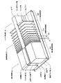
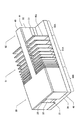
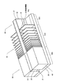
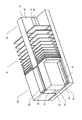
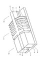
【解決手段】 基板上に、コアの両側が第1の媒質で埋め込まれている埋込導波路が形成されている。さらに、基板の上に、コアの両側に、第1の媒質よりも屈折率の小さな第2の媒質が配置されているハイメサ導波路が形成されている。さらに、基板の上に、埋込導波路とハイメサ導波路とを光学的に接続する接続導波路が形成されている。接続導波路は、接続導波路のコアの少なくとも一方の側に配置され、導波方向に並ぶ複数のフィンを含む。
【選択図】 図1
Description
基板上に形成され、コアの両側が第1の媒質で埋め込まれている埋込導波路と、
前記基板の上に形成され、コアの両側に、前記第1の媒質よりも屈折率の小さな第2の媒質が配置されているハイメサ導波路と、
前記基板の上に形成され、前記埋込導波路と前記ハイメサ導波路とを光学的に接続する接続導波路と
を有し、前記接続導波路は、該接続導波路のコアの少なくとも一方の側に配置され、導波方向に並ぶ複数のフィンを含む。
21 コア層
22 上部クラッド層
23 コンタクト層
25 下部クラッド層
31 コア層
32 上部クラッド層
40 第1のマスクパターン
41 メサ
45 電流ブロック層
45a フィン
48 第2のマスクパターン
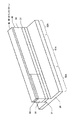
50 埋込導波路
50A 埋込導波路領域
51 接続導波路
51A 接続導波路領域
52 ハイメサ導波路
52A ハイメサ導波路領域
60 側面被覆膜
65 コア層の境界
66 埋込導波路と接続導波路との境界
70 上部電極
71 背面電極
72 下部電極
Claims (5)
- 基板上に形成され、コアの両側が第1の媒質で埋め込まれている埋込導波路と、
前記基板の上に形成され、コアの両側に、前記第1の媒質よりも屈折率の小さな第2の媒質が配置されているハイメサ導波路と、
前記基板の上に形成され、前記埋込導波路と前記ハイメサ導波路とを光学的に接続する接続導波路と
を有し、前記接続導波路は、該接続導波路のコアの少なくとも一方の側に配置され、導波方向に並ぶ複数のフィンを含む光導波装置。 - 前記フィンは、前記第1の媒質と同一の媒質で形成されている請求項1に記載の光導波装置。
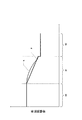
- 前記接続導波路の等価屈折率が、前記埋込導波路から前記ハイメサ導波路に向かって低下している請求項1または2に記載の光導波装置。
- 相互に隣り合う前記フィンの間の間隙部の厚さが、前記埋込導波路から前記ハイメサ導波路に近づくにつれて厚くなるように変化している請求項1乃至3のいずれか1項に記載の光導波装置。
- 前記フィンの厚さが、前記埋込導波路から前記ハイメサ導波路に近づくにつれて薄くなるように変化している請求項1乃至4のいずれか1項に記載の光導波装置。
Priority Applications (1)
| Application Number | Priority Date | Filing Date | Title |
|---|---|---|---|
| JP2008240526A JP5326456B2 (ja) | 2008-09-19 | 2008-09-19 | 光導波装置 |
Applications Claiming Priority (1)
| Application Number | Priority Date | Filing Date | Title |
|---|---|---|---|
| JP2008240526A JP5326456B2 (ja) | 2008-09-19 | 2008-09-19 | 光導波装置 |
Publications (2)
| Publication Number | Publication Date |
|---|---|
| JP2010072401A true JP2010072401A (ja) | 2010-04-02 |
| JP5326456B2 JP5326456B2 (ja) | 2013-10-30 |
Family
ID=42204225
Family Applications (1)
| Application Number | Title | Priority Date | Filing Date |
|---|---|---|---|
| JP2008240526A Expired - Fee Related JP5326456B2 (ja) | 2008-09-19 | 2008-09-19 | 光導波装置 |
Country Status (1)
| Country | Link |
|---|---|
| JP (1) | JP5326456B2 (ja) |
Cited By (2)
| Publication number | Priority date | Publication date | Assignee | Title |
|---|---|---|---|---|
| JP2011258810A (ja) * | 2010-06-10 | 2011-12-22 | Mitsubishi Electric Corp | 半導体光集積素子及びその製造方法 |
| US12352988B2 (en) | 2020-06-03 | 2025-07-08 | Applied Materials, Inc. | Gradient encapsulation of waveguide gratings |
Citations (2)
| Publication number | Priority date | Publication date | Assignee | Title |
|---|---|---|---|---|
| JP2002258086A (ja) * | 2001-02-27 | 2002-09-11 | Kyocera Corp | 光導波路および光回路基板 |
| JP2002311267A (ja) * | 2001-04-12 | 2002-10-23 | Nippon Telegr & Teleph Corp <Ntt> | 接続型光導波路 |
-
2008
- 2008-09-19 JP JP2008240526A patent/JP5326456B2/ja not_active Expired - Fee Related
Patent Citations (2)
| Publication number | Priority date | Publication date | Assignee | Title |
|---|---|---|---|---|
| JP2002258086A (ja) * | 2001-02-27 | 2002-09-11 | Kyocera Corp | 光導波路および光回路基板 |
| JP2002311267A (ja) * | 2001-04-12 | 2002-10-23 | Nippon Telegr & Teleph Corp <Ntt> | 接続型光導波路 |
Cited By (2)
| Publication number | Priority date | Publication date | Assignee | Title |
|---|---|---|---|---|
| JP2011258810A (ja) * | 2010-06-10 | 2011-12-22 | Mitsubishi Electric Corp | 半導体光集積素子及びその製造方法 |
| US12352988B2 (en) | 2020-06-03 | 2025-07-08 | Applied Materials, Inc. | Gradient encapsulation of waveguide gratings |
Also Published As
| Publication number | Publication date |
|---|---|
| JP5326456B2 (ja) | 2013-10-30 |
Similar Documents
| Publication | Publication Date | Title |
|---|---|---|
| JP7267370B2 (ja) | 光半導体素子、光モジュール及び光半導体素子の製造方法 | |
| JP5897414B2 (ja) | 光デバイスの製造方法 | |
| EP0641049B1 (en) | An optical semiconductor device and a method of manufacturing the same | |
| US7835418B2 (en) | Optical semiconductor device having diffraction grating disposed on both sides of waveguide and its manufacture method | |
| US10511147B2 (en) | Laser device and process for fabricating such a laser device | |
| EP0378098B1 (en) | Semiconductor optical device | |
| US8558245B2 (en) | Optical semiconductor device having ridge structure formed on active layer containing p-type region and its manufacture method | |
| CN111711074B (zh) | 激光器及其制作方法 | |
| JP5314435B2 (ja) | 集積光デバイス及びその製造方法 | |
| US20080199128A1 (en) | Semiconductor integrated optical element | |
| US20130207140A1 (en) | Semiconductor Optical Element Semiconductor Optical Module and Manufacturing Method Thereof | |
| CN107706738A (zh) | 分布反馈半导体激光器及其制备方法 | |
| JP6084428B2 (ja) | 半導体光集積素子及びその製造方法 | |
| JP5326456B2 (ja) | 光導波装置 | |
| CN112072470A (zh) | 多波长激光器阵列及其制作方法 | |
| US8731344B2 (en) | Method for manufacturing semiconductor optical modulator and semiconductor optical modulator | |
| JP5957856B2 (ja) | 半導体集積素子 | |
| JP5029239B2 (ja) | 半導体光素子およびその製造方法 | |
| JPH0548214A (ja) | 分布反射型半導体レーザ | |
| EP0332723A1 (en) | High-power semiconductor diode laser | |
| JP7410276B2 (ja) | 半導体光デバイス | |
| JP4769778B2 (ja) | 光半導体素子及びその製造方法 | |
| JP2002057405A (ja) | 半導体レーザ装置及びその製造方法 | |
| CN112821197A (zh) | 一种光发射芯片的制作方法和光发射芯片 | |
| JP7661500B2 (ja) | 量子井戸構造、チップ加工方法及びチップ |
Legal Events
| Date | Code | Title | Description |
|---|---|---|---|
| A621 | Written request for application examination |
Free format text: JAPANESE INTERMEDIATE CODE: A621 Effective date: 20110613 |
|
| A131 | Notification of reasons for refusal |
Free format text: JAPANESE INTERMEDIATE CODE: A131 Effective date: 20120522 |
|
| A977 | Report on retrieval |
Free format text: JAPANESE INTERMEDIATE CODE: A971007 Effective date: 20120523 |
|
| A131 | Notification of reasons for refusal |
Free format text: JAPANESE INTERMEDIATE CODE: A131 Effective date: 20130226 |
|
| A521 | Request for written amendment filed |
Free format text: JAPANESE INTERMEDIATE CODE: A523 Effective date: 20130416 |
|
| TRDD | Decision of grant or rejection written | ||
| A01 | Written decision to grant a patent or to grant a registration (utility model) |
Free format text: JAPANESE INTERMEDIATE CODE: A01 Effective date: 20130625 |
|
| A61 | First payment of annual fees (during grant procedure) |
Free format text: JAPANESE INTERMEDIATE CODE: A61 Effective date: 20130708 |
|
| R150 | Certificate of patent or registration of utility model |
Ref document number: 5326456 Country of ref document: JP Free format text: JAPANESE INTERMEDIATE CODE: R150 Free format text: JAPANESE INTERMEDIATE CODE: R150 |
|
| LAPS | Cancellation because of no payment of annual fees |