JP2010068566A - Step-up switching power supply circuit - Google Patents
Step-up switching power supply circuit Download PDFInfo
- Publication number
- JP2010068566A JP2010068566A JP2008230307A JP2008230307A JP2010068566A JP 2010068566 A JP2010068566 A JP 2010068566A JP 2008230307 A JP2008230307 A JP 2008230307A JP 2008230307 A JP2008230307 A JP 2008230307A JP 2010068566 A JP2010068566 A JP 2010068566A
- Authority
- JP
- Japan
- Prior art keywords
- switching element
- switching
- power supply
- supply circuit
- turned
- Prior art date
- Legal status (The legal status is an assumption and is not a legal conclusion. Google has not performed a legal analysis and makes no representation as to the accuracy of the status listed.)
- Granted
Links
- 239000003990 capacitor Substances 0.000 claims description 7
- 230000000087 stabilizing effect Effects 0.000 claims description 3
- 238000010586 diagram Methods 0.000 description 10
- 230000003071 parasitic effect Effects 0.000 description 4
- 230000006378 damage Effects 0.000 description 2
- 238000009499 grossing Methods 0.000 description 2
- 244000145845 chattering Species 0.000 description 1
- 230000003111 delayed effect Effects 0.000 description 1
- 230000012447 hatching Effects 0.000 description 1
- 230000000630 rising effect Effects 0.000 description 1
Images


Classifications
-
- H—ELECTRICITY
- H02—GENERATION; CONVERSION OR DISTRIBUTION OF ELECTRIC POWER
- H02M—APPARATUS FOR CONVERSION BETWEEN AC AND AC, BETWEEN AC AND DC, OR BETWEEN DC AND DC, AND FOR USE WITH MAINS OR SIMILAR POWER SUPPLY SYSTEMS; CONVERSION OF DC OR AC INPUT POWER INTO SURGE OUTPUT POWER; CONTROL OR REGULATION THEREOF
- H02M3/00—Conversion of dc power input into dc power output
- H02M3/02—Conversion of dc power input into dc power output without intermediate conversion into ac
- H02M3/04—Conversion of dc power input into dc power output without intermediate conversion into ac by static converters
- H02M3/10—Conversion of dc power input into dc power output without intermediate conversion into ac by static converters using discharge tubes with control electrode or semiconductor devices with control electrode
- H02M3/145—Conversion of dc power input into dc power output without intermediate conversion into ac by static converters using discharge tubes with control electrode or semiconductor devices with control electrode using devices of a triode or transistor type requiring continuous application of a control signal
- H02M3/155—Conversion of dc power input into dc power output without intermediate conversion into ac by static converters using discharge tubes with control electrode or semiconductor devices with control electrode using devices of a triode or transistor type requiring continuous application of a control signal using semiconductor devices only
- H02M3/156—Conversion of dc power input into dc power output without intermediate conversion into ac by static converters using discharge tubes with control electrode or semiconductor devices with control electrode using devices of a triode or transistor type requiring continuous application of a control signal using semiconductor devices only with automatic control of output voltage or current, e.g. switching regulators
-
- H—ELECTRICITY
- H02—GENERATION; CONVERSION OR DISTRIBUTION OF ELECTRIC POWER
- H02M—APPARATUS FOR CONVERSION BETWEEN AC AND AC, BETWEEN AC AND DC, OR BETWEEN DC AND DC, AND FOR USE WITH MAINS OR SIMILAR POWER SUPPLY SYSTEMS; CONVERSION OF DC OR AC INPUT POWER INTO SURGE OUTPUT POWER; CONTROL OR REGULATION THEREOF
- H02M1/00—Details of apparatus for conversion
- H02M1/36—Means for starting or stopping converters
Landscapes
- Engineering & Computer Science (AREA)
- Power Engineering (AREA)
- Dc-Dc Converters (AREA)
Abstract
Description
本発明は昇圧形スイッチング電源回路に関し、特に当該スイッチング電源回路の昇圧動作の停止時に電源による入力電圧が出力端子に印加されるのを防止する構造を採用する場合に適用して有用なものである。 The present invention relates to a step-up switching power supply circuit, and is particularly useful when applied to a structure that prevents an input voltage from a power source from being applied to an output terminal when the step-up operation of the switching power supply circuit is stopped. .
スイッチング電源回路の中には、電源電圧を昇圧して出力する、いわゆる昇圧形のものがある。図6は従来技術に係る代表的な昇圧形スイッチング電源回路を示す回路図である。同図に示すように、当該スイッチング電源回路では、N形のMOSFETで形成したスイッチング素子SW1をオンさせると、電源1からコイルL及びスイッチング素子SW1を介してコイル電流ILが流れることによりコイルLにエネルギが蓄積される。その後スイッチング素子SW1をオフさせるとスイッチング素子SW1のオン期間に蓄積されたエネルギに基づく逆起電力が電源1の出力である入力電圧VINに重畳される。この結果、所定電圧に昇圧された出力電圧VOUTをショットキーダイオードSBDを介して出力端子OUTに得ることができる。ここで、コンデンサCLは出力電流IOUTの平滑用として、コンデンサCFBは位相補償用として機能する。
Among switching power supply circuits, there is a so-called boost type circuit that boosts and outputs a power supply voltage. FIG. 6 is a circuit diagram showing a typical step-up switching power supply circuit according to the prior art. As shown in the figure, in the switching power supply circuit, when a switching element SW1 formed of an N-type MOSFET is turned on, a coil current IL flows from the
一方、出力端子OUTにおける出力電圧VOUTは抵抗RFB1及び抵抗RFB2で所定の割合に分圧されてエラーアンプ2の一方の入力端子に供給される。エラーアンプ2は出力電圧VOUTを分圧した電圧と、他方の入力端子に供給されている予め定めた基準電圧VREFとの偏差を表す誤差信号Verrを出力する。PWMコンパレータ3は誤差信号Verrと、ランプ発生器4が発生するランプ信号RAMPとを比較して形成したPWM信号PWMを出力する。スイッチング素子SW1はスイッチング制御回路5によりPWM信号PWMに基づきそのオン・オフが制御される。かくして、PWM信号PWMのデューティに基づきスイッチング素子SW1のオン期間を制御することにより出力電圧VOUTを所定値に調整する。なお、位相補償回路6はエラーアンプ2の高周波数帯域での位相補償を行うものである。
On the other hand, the output voltage VOUT at the output terminal OUT is divided into a predetermined ratio by the resistors RFB1 and RFB2 and supplied to one input terminal of the
ところで、かかる昇圧形スイッチング電源回路では、当該昇圧形スイッチング電源回路の昇圧動作を停止するに際し、スイッチング素子SW1のスイッチング制御を停止しても入力電圧VINが出力端子OUTにそのまま出力されてしまう。 By the way, in such a step-up switching power supply circuit, when the step-up operation of the step-up switching power supply circuit is stopped, the input voltage VIN is output to the output terminal OUT as it is even if the switching control of the switching element SW1 is stopped.
かかる問題はショットキーダイオードSBDの代わりにスイッチング素子を用いてこのスイッチング素子で電源側と負荷側とを遮断することにより一応解決する。ところが、この場合のスイッチング素子をMOSFETで形成した場合、MOSFETが本来的に有する寄生ダイオードにより電源側と負荷側とが接続されてしまうという問題が発生する。 Such a problem is temporarily solved by using a switching element instead of the Schottky diode SBD and shutting off the power supply side and the load side with this switching element. However, when the switching element in this case is formed of a MOSFET, there arises a problem that the power supply side and the load side are connected by a parasitic diode inherent in the MOSFET.
かかる問題を解決する昇圧形スイッチング電源回路を開示する公知文献として特許文献1が存在する。特許文献1に開示する昇圧形スイッチング電源回路は、コイルの出力側と出力端子との間に接続されたP形のスイッチング素子である第1のMOSFETに対し、前記出力端子と前記第1のMOSFETのバックゲートとの間に接続されるとともにゲートが入力端子に接続されたP形のスイッチング素子である第2のMOSFETと、前記入力端子と前記第1のMOSFETのバックゲートとの間に接続されるとともにゲートが前記出力端子に接続されたP形のスイッチング素子である第3のMOSFETとを追加して構成したものである。
かかる構成により、昇圧動作の停止時には第1のMOSFETを介する電流経路は元より、これに付随する寄生ダイオードを介した電流経路をも第2のMOSFETにより遮断することができる。
一般に、MOSFETはそのバックゲートの電位がフローティング状態の場合には、ラッチアップによる素子破壊の虞がある。しかしながら、特許文献1に開示する昇圧形スイッチング回路ではその始動時には第1乃至第3のMOSFETが何れもオフ状態であるので、それぞれのバックゲートの電圧は不定である。
In general, when the potential of the back gate of a MOSFET is in a floating state, there is a risk of element destruction due to latch-up. However, in the step-up switching circuit disclosed in
さらに、特許文献1に開示する昇圧形スイッチング回路の始動時には第1のMOSFETに大きな突入電流が流れるという問題もある。
Furthermore, there is also a problem that a large inrush current flows through the first MOSFET when the step-up switching circuit disclosed in
本発明は、上記従来技術に鑑み、昇圧動作停止時に入力電圧が出力に生じないよう負荷切断が可能であるばかりでなく、MOSFETのバックゲートの電位を固定するとともに、始動時の突入電流を有効に抑制し得る昇圧形スイッチング電源回路を提供することを目的とする。 In view of the above-described prior art, the present invention not only enables load disconnection so that an input voltage is not generated at the output when the boost operation is stopped, but also fixes the potential of the back gate of the MOSFET and enables inrush current at start-up. An object of the present invention is to provide a step-up switching power supply circuit that can be suppressed to a low level.
上記目的を達成するための本発明の第1の態様は、出力電圧と基準値との偏差を検出するエラーアンプの出力信号に基づき第1のスイッチング素子を制御するとともに、コイルに蓄積したエネルギに基づく電圧を入力電圧に重畳することにより昇圧した出力電圧を出力端子を介して得る昇圧形スイッチング電源回路であって、前記コイルの出力側と前記出力端子との間に接続されたP形のMOSFETからなる第2のスイッチング素子と、アノードが前記コイルの出力側にされた第1のダイオードと、アノードが前記出力端子に接続され、そのカソードと前記第1のダイオードのカソードとが相互に接続されるとともに両者の接続点が前記第2のスイッチング素子のバックゲートに接続されている第2のダイオードと、前記コイルの出力側と前記第2のスイッチング素子のバックゲートとの間に接続されるとともに、自身のバックゲートが前記第2のスイッチング素子のバックゲートに接続されたP形のMOSFETからなる第3のスイッチング素子と、前記出力端子と前記第2のスイッチング素子のバックゲートとの間に接続されるとともに、自身のバックゲートが前記第2のスイッチング素子のバックゲートに接続されたP形のMOSFETからなる第4のスイッチング素子と、昇圧動作のための制御の開始を一定時間遅延させる遅延手段と、前記遅延手段による遅延期間内において前記第2のスイッチング素子を定電流駆動する定電流駆動手段と、前記遅延期間の経過後に前記第1のスイッチング素子と前記第2のスイッチング素子とを交互にオン・オフ制御する第1のスイッチング制御手段と、前記昇圧動作のための制御の停止時又は前記遅延期間内においてコンパレータで比較する前記入力電圧が前記出力電圧よりも大きいときは前記第3のスイッチング素子がオンするとともに前記第4のスイッチング素子がオフするように、また前記コンパレータで比較する前記入力電圧が前記出力電圧よりも小さいときは前記第3のスイッチング素子がオフするとともに前記第4のスイッチング素子がオンし、さらに前記遅延期間の経過後には前記コンパレータで比較する前記入力電圧と前記出力電圧との大小関係の如何にかかわらず前記第3のスイッチング素子がオフするとともに前記第4のスイッチング素子がオンするようにスイッチング制御を行う第2のスイッチング制御手段とを有することを特徴とする昇圧形スイッチング電源回路にある。 The first aspect of the present invention for achieving the above object is to control the first switching element based on the output signal of the error amplifier that detects the deviation between the output voltage and the reference value, and to store the energy stored in the coil. A step-up switching power supply circuit that obtains an output voltage boosted by superimposing a voltage based on an input voltage via an output terminal, the P-type MOSFET being connected between the output side of the coil and the output terminal A first diode having an anode on the output side of the coil, an anode connected to the output terminal, and a cathode connected to the cathode of the first diode. And a second diode whose connection point is connected to the back gate of the second switching element; and an output side of the coil; A third switching element comprising a P-type MOSFET connected between the back gate of the second switching element and having its own back gate connected to the back gate of the second switching element; A fourth switching element comprising a P-type MOSFET connected between the output terminal and the back gate of the second switching element, the back gate of which is connected to the back gate of the second switching element; Delay means for delaying the start of control for boosting operation for a fixed time, constant current drive means for constant current driving the second switching element within a delay period by the delay means, and after the delay period has elapsed A first switch for alternately turning on and off the first switching element and the second switching element. The third switching element is turned on and the fourth switching element is turned on when the input voltage to be compared by the comparator when the control for the boosting operation is stopped or during the delay period is larger than the output voltage. And when the input voltage to be compared by the comparator is smaller than the output voltage, the third switching element is turned off and the fourth switching element is turned on, and the delay After the elapse of the period, switching control is performed so that the third switching element is turned off and the fourth switching element is turned on regardless of the magnitude relationship between the input voltage and the output voltage compared by the comparator. And a second switching control means for performing the boosting switch. In the power supply circuit.
本発明の第2の態様は、第1の態様に記載する昇圧形スイッチング電源回路において、
前記コンパレータは前記入力電圧に所定の電圧を重畳した電圧と前記出力電圧とを比較するように構成したことを特徴とする昇圧形スイッチング電源回路にある。
According to a second aspect of the present invention, in the step-up switching power supply circuit described in the first aspect,
The comparator is a step-up switching power supply circuit configured to compare a voltage obtained by superimposing a predetermined voltage on the input voltage and the output voltage.
本発明の第3の態様は、第1又は第2の態様に記載する昇圧形スイッチング電源回路において、電源電圧は前記コンパレータの出力に基づき前記入力電圧乃至前記出力電圧のうち大きい方を選択して使用するように構成したことを特徴とする昇圧形スイッチング電源回路にある。 According to a third aspect of the present invention, in the step-up switching power supply circuit described in the first or second aspect, the power supply voltage is selected from the input voltage to the output voltage based on the output of the comparator. A step-up switching power supply circuit is characterized by being configured to be used.
本発明の第4の態様は、第1乃至第3の態様の何れか一つに記載する昇圧形スイッチング電源回路において、前記第1のスイッチング制御手段と前記第2のスイッチング素子のゲートとの間にバッファ回路を設け、このバッファ回路は前記遅延期間内において停止され、前記遅延期間経過後に前記第1のスイッチング制御手段のスイッチング制御に基づき前記第2のスイッチング素子のオン・オフ制御を行うように構成したものであることを特徴とする昇圧形スイッチング電源回路にある。 According to a fourth aspect of the present invention, there is provided the step-up switching power supply circuit according to any one of the first to third aspects, between the first switching control means and the gate of the second switching element. Provided with a buffer circuit, and the buffer circuit is stopped within the delay period, and on / off control of the second switching element is performed based on switching control of the first switching control means after the delay period elapses. A step-up switching power supply circuit is characterized in that it is configured.
本発明の第5の態様は、第1乃至第4の態様の何れか一つに記載する昇圧形スイッチング電源回路は集積回路で構成したことを特徴とする昇圧形スイッチング電源回路にある。 According to a fifth aspect of the present invention, there is provided a step-up switching power supply circuit characterized in that the step-up switching power supply circuit described in any one of the first to fourth aspects is constituted by an integrated circuit.
本発明の第6の態様は、第5の態様に記載する昇圧形スイッチング電源において、前記遅延手段はイネーブル回路が前記集積回路を駆動可能になった時点から前記昇圧動作のための制御の開始を一定時間遅延するように構成したことを特徴とする昇圧形スイッチング電源回路にある。 According to a sixth aspect of the present invention, in the step-up switching power supply according to the fifth aspect, the delay means starts control for the step-up operation from the time when the enable circuit can drive the integrated circuit. A step-up switching power supply circuit is configured to be delayed for a predetermined time.
本発明の第7の態様は、第5又は第6の態様に記載する昇圧形スイッチング電源回路において、前記集積回路には、この集積回路の動作を安定させるための外付けコンデンサを接続可能なピンを有することを特徴とする昇圧形スイッチング電源回路にある。 According to a seventh aspect of the present invention, in the step-up switching power supply circuit described in the fifth or sixth aspect, the integrated circuit is connected to an external capacitor for stabilizing the operation of the integrated circuit. The step-up type switching power supply circuit is characterized by comprising:
本発明によれば、昇圧動作の停止時に入力側から出力側に至る電流経路は第2のダイオードで遮断される結果、入力電圧が出力端子に表れることはない。その上、第2のスイッチング制御手段によるオン・オフ制御で当該昇圧形スイッチング回路の始動時においてもMOSFET素子で形成した第3乃至第4のスイッチング素子のオン・オフ状態が確定され、第3乃至第4のスイッチング素子が同時にオフ状態となることはない。この結果、バックゲート同士が接続されている第2乃至第4のバックゲートの電位が不定となることはなく、ラッチ電流等による前記スイッチング素子の動作の不安定乃至破壊を未然に防止し得る。 According to the present invention, when the step-up operation is stopped, the current path from the input side to the output side is blocked by the second diode, so that the input voltage does not appear at the output terminal. In addition, the on / off control by the second switching control means determines the on / off states of the third to fourth switching elements formed by the MOSFET elements even when the boosting switching circuit is started. The fourth switching element is not simultaneously turned off. As a result, the potentials of the second to fourth back gates to which the back gates are connected do not become indefinite, and instability or destruction of the operation of the switching element due to a latch current or the like can be prevented.
さらに、第2のスイッチング素子は、当該昇圧形スイッチング電源回路の始動時の一定期間、定電流駆動手段により定電流駆動されるので、第2のスイッチング素子に大きな始動電流が流れることもない。 Further, since the second switching element is driven with a constant current by the constant current driving means for a certain period of time when the boosting switching power supply circuit is started, a large starting current does not flow through the second switching element.
以下本発明の実施の形態及び実施例を図面に基づき詳細に説明する。 Hereinafter, embodiments and examples of the present invention will be described in detail with reference to the drawings.
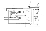
<第1の実施の形態>
図1は本発明の第1の実施の形態に係るスイッチング電源回路の制御回路を示す回路図である。本形態は、図6に示す昇圧形スイッチング電源回路に所定の制御回路を追加したものである。そこで図6と同一部分には同一番号を付し、重複する説明は省略する。
<First Embodiment>
FIG. 1 is a circuit diagram showing a control circuit of a switching power supply circuit according to the first embodiment of the present invention. In this embodiment, a predetermined control circuit is added to the step-up switching power supply circuit shown in FIG. Therefore, the same parts as those in FIG.
図1に示すように、P形のMOSFETで形成した第2のスイッチング素子SW2は、コイルLの出力側と出力端子OUTとの間に接続されており、N形のMOSFETで形成した第1のスイッチング素子SW1と交互にオン・オフされる。第2のスイッチング素子SW2の一つの寄生ダイオードである第1のダイオードD1はそのアノードがコイルLの出力側に接続されており、他の寄生ダイオードである第2のダイオードD2はそのアノードが出力端子OUTに接続されている。また、第1のダイオードD1のカソードと第2のダイオードD2のカソードとは相互に接続されるとともに両者の接続点が第2のスイッチング素子SW2のバックゲートに接続されている。 As shown in FIG. 1, the second switching element SW2 formed of a P-type MOSFET is connected between the output side of the coil L and the output terminal OUT, and the first switching element SW2 formed of an N-type MOSFET is used. It is turned on / off alternately with the switching element SW1. The first diode D1, which is one parasitic diode of the second switching element SW2, has its anode connected to the output side of the coil L, and the second diode D2, which is another parasitic diode, has its anode as an output terminal. Connected to OUT. The cathode of the first diode D1 and the cathode of the second diode D2 are connected to each other, and the connection point between them is connected to the back gate of the second switching element SW2.
P形のMOSFETで形成した第3のスイッチング素子SW3は、コイルLの出力側と第2のスイッチング素子SW2のバックゲートとの間にそのバックゲートとともに接続されている。P形のMOSFETで形成した第4のスイッチング素子SW4は、出力端子OUTと第2のスイッチング素子SW2のバックゲートとの間にそのバックゲートとともに接続されている。 The third switching element SW3 formed of a P-type MOSFET is connected between the output side of the coil L and the back gate of the second switching element SW2 together with the back gate. The fourth switching element SW4 formed of a P-type MOSFET is connected with the back gate between the output terminal OUT and the back gate of the second switching element SW2.
イネーブル回路7は各回路素子の動作を許容するイネーブル信号Dを遅延回路8及び定電流源バッファ回路9に送出する。遅延回路8はイネーブル信号Dの立ち上がりを一定時間遅延させた遅延信号Cを定電流源バッファ回路9及びスイッチング制御回路15に送出する。
The
スイッチング制御回路15は遅延信号Cで規定される遅延期間の経過後、第1のスイッチング素子SW1と第2のスイッチング素子SW2とを交互にオン・オフ制御する。スイッチング制御回路15による第2のスイッチング素子SW2のスイッチング制御は、定電流源バッファ回路9にスイッチング制御信号Bを供給することにより形成されるスイッチング制御信号Eを介して行われる(この点については後に詳説する。)。
The switching
定電流源バッファ回路9は、この部分を抽出して図2に詳細に示すように、定電流回路10及びバッファ回路11を有している。かかる、定電流源バッファ回路9の動作は、後に詳説するが、イネーブル信号Dが立ち上がり、遅延回路8に設定された遅延期間が経過するまで、すなわち遅延信号Cが立ち上がるまではバッファ回路11の動作が停止され、定電流回路10の基準電源VREF1に基づく定電圧の信号であるスイッチング制御信号Eが定電流回路10からスイッチング素子SW2のゲートに供給される。この結果、スイッチング素子SW2には所定の定電流が流れる。このとき、イネーブル信号D、スイッチング制御信号B及びスイッチング制御信号Fを論理回路の入力とするバッファ回路11の出力段のスイッチング素子SW5,SW6は何れもオフ状態となっている。一方、遅延期間の経過後には、定電流回路10の動作が停止され、バッファ回路11を介してスイッチング制御回路15によるスイッチング素子SW2のスイッチング制御が行われる。
The constant current
スイッチング素子SW3,SW4は、コンパレータ12、ノア回路13、インバータ14からなる論理回路でスイッチング制御される。ここで、コンパレータ12は出力電圧VOUTと入力電圧VINとを比較し、VOUT>VINのときその出力信号AがH状態となる。ノア回路13の一方の入力端子には出力信号Aが供給されるとともに他方の入力端子には遅延信号Cが供給され、その出力信号がスイッチング制御信号Fとなってスイッチング素子SW4のゲートに供給される。スイッチング素子SW3のゲートにはスイッチング制御信号Fをインバータ14で反転させたスイッチング制御信号F´が供給される。したがって、当該回路における昇圧動作のための制御の停止時、又は遅延信号Cによる遅延期間内において、VOUT<VINのときには第3のスイッチング素子SW3がオン状態とされ、同時にスイッチング素子SW4がオフ状態とされる。また、VOUT>VINのときには、逆に第3のスイッチング素子SW3がオフ状態とされ、同時にスイッチング素子SW4がオン状態とされる。一方、遅延信号Cによる遅延期間の経過後にはコンパレータ12で比較する出力電圧VOUTと入力電圧VINとの大小関係の如何にかかわらず第3のスイッチング素子SW3がオフ状態となり、第4のスイッチング素子SW4がオン状態となるように制御される。
Switching elements SW3 and SW4 are controlled by a logic circuit including a
電源電圧選択回路16は、コンパレータ12の出力信号Aに基づき入力電圧VINと出力電圧VOUTのうち大きい方を選択して電源電圧VDDとするためのものである。さらに詳言すると、この部分を抽出して図3に示すように、当該電源電圧選択回路16はスイッチング素子SW7、SW8を有しており、出力信号Aによりスイッチング素子SW7がオン状態にされた場合には、入力電圧VINが選択され、スイッチング素子SW8がオン状態にされた場合には、出力電圧VOUTが選択されてそれぞれ電源電圧VDDとなる。
当該昇圧形スイッチング電源回路のうち、電源1、コイルL及び平滑用のコンデンサCLを除く各回路素子は集積回路ICとして集積されている。ここで、集積回路ICはその動作を安定させるための外付けコンデンサCDDを接続可能なピンPを有しており、このピンPを介してコンデンサCDDが接続してある。
The power supply
Of the step-up switching power supply circuit, circuit elements other than the
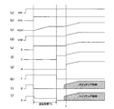
かかる本形態の動作を図4の波形図を追加して説明する。先ず、電源1の投入により入力電圧VINが立ち上がる(図4(a)参照)。これにより、電源電圧VDD(図4(d)参照)、スイッチング制御信号F,B,E(図4(h)、(i)、(j)参照)が立ち上がる。
The operation of this embodiment will be described with reference to the waveform diagram of FIG. First, the input voltage VIN rises when the
次に、イネーブル電圧信号VEN(図4(b))の立ち上がりによりイネーブル信号D(図4(e))が立ち上がることにより集積回路ICの各部の動作が開始される。すなわち、遅延回路8における遅延動作が開始され、所定の遅延期間TDの経過後、遅延信号Cが立ち上がる(図4(f)参照)。また、遅延期間TDにおいて出力電圧VOUT(図4(c))と入力電圧VINとの関係は、VIN>VOUTとなっているので、コンパレータ12の出力信号A(図4(g)参照)はL状態となっており、この結果スイッチング素子SW3がオン状態で、スイッチング素子SW4がオフ状態に制御される。すなわち、スイッチング素子SW2,SW3,SW4のバックゲートの電位がフローティング状態となることはない。
Next, the operation of each part of the integrated circuit IC is started when the enable signal D (FIG. 4E) rises with the rise of the enable voltage signal VEN (FIG. 4B). That is, the delay operation in the
遅延期間TDにおいてはスイッチング制御信号FがH状態であり、この結果バッファ回路11(図2参照;以下同じ。)のスイッチング素子SW5,SW6が何れもオフ状態に制御されているので、このバッファ回路11からスイッチング制御信号Eが送出されることはない。一方、遅延期間TDにおいては遅延信号CがL状態であり、この結果定電流回路10(図2参照;以下同じ。)からは基準電源VREF1に基づく定電圧の信号であるスイッチング制御信号Eがスイッチング素子SW2のゲートに供給される。この結果、スイッチング素子SW2は所定の定電流で動作を開始する。すなわち、遅延期間TDを設けてこの遅延期間TDには定電流を流すように制御することで始動時の突入電流を抑制することができる。 In the delay period TD, the switching control signal F is in the H state. As a result, the switching elements SW5 and SW6 of the buffer circuit 11 (see FIG. 2; the same applies hereinafter) are both controlled to be in the off state. No switching control signal E is sent from 11. On the other hand, in the delay period TD, the delay signal C is in the L state. As a result, the constant current circuit 10 (see FIG. 2; the same applies hereinafter) switches the switching control signal E, which is a constant voltage signal based on the reference power supply VREF1. It is supplied to the gate of the element SW2. As a result, the switching element SW2 starts operation with a predetermined constant current. That is, by providing a delay period TD and controlling the constant period to flow during this delay period TD, the inrush current at the start can be suppressed.
また、昇圧動作のための制御の停止時又は遅延期間TD内においてコンパレータ12で比較する入力電圧VINが出力電圧VOUTよりも大きいときはスイッチング素子SW3がオンするとともにスイッチング素子SW4がオフするように制御される。このことにより入力電圧VINに起因して出力側に向かって流れようとする電流はダイオードD2でブロックされる。この結果、入力電圧VINの影響が出力側に及ぶことはない。
Further, when the control for boosting operation is stopped or when the input voltage VIN compared by the
昇圧動作のための制御の停止時、コンパレータ12で比較する入力電圧VINが出力電圧VOUTよりも小さいときはスイッチング素子SW3がオフするとともにスイッチング素子SW4がオンするように制御する。このことにより、出力電圧VOUTに起因して入力側に向かって流れようとする電流はダイオードD1でブロックされる。この結果、出力電圧VOUTの影響が出力側に及ぶことはない。
When the control for the boosting operation is stopped, when the input voltage VIN compared by the
遅延期間TDの経過後、遅延信号Cの立ち上がりにより定電流回路10の動作が停止される。一方、遅延期間TDの経過後、スイッチング制御信号Fが立ち下がることによりスイッチング制御信号B,Eによる通常のスイッチング制御(図4(i)、(j)中に斜線で示す領域)が開始される。ちなみに、遅延期間TDの経過後にはコンパレータ12で比較する入力電圧VINと出力電圧VOUTとの大小関係の如何にかかわらずスイッチング素子SW3がオフするとともにスイッチング素子SW4がオンするように制御される。
After the lapse of the delay period TD, the operation of the constant
ここで、出力電圧VOUTはイネーブル信号Dの立ち上がりに伴い漸増し、一定値になった後、前記スイッチング制御の開始に伴い再度漸増する。この結果、前記スイッチング制御が開始された直後のあるタイミングTで入力電圧VIN<出力電圧VOUTとなる。この結果、図3に基づき説明したように、電源電圧VDDはそれまでの入力電圧VINに代わって出力電圧VOUTが選択される。これに伴い、イネーブル信号D、遅延信号C、出力信号Aも電源電圧VDDに追従して漸増する。 Here, the output voltage VOUT gradually increases as the enable signal D rises, and after reaching a constant value, gradually increases again as the switching control starts. As a result, the input voltage VIN <the output voltage VOUT is satisfied at a certain timing T immediately after the switching control is started. As a result, as described with reference to FIG. 3, the output voltage VOUT is selected as the power supply voltage VDD instead of the input voltage VIN so far. Along with this, the enable signal D, the delay signal C, and the output signal A also gradually increase following the power supply voltage VDD.
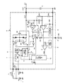
<第2の実施の形態>
図5は本発明の第2の実施の形態に係るスイッチング電源回路の制御回路を示す回路図である。本形態は、図1に示す昇圧形スイッチング電源回路のコンパレータ12の構成を変更したものであり、その他に構成は図1と全く同様である。そこで、図1と同一部分には同一番号を付し、重複する説明は省略する。
<Second Embodiment>
FIG. 5 is a circuit diagram showing a control circuit of the switching power supply circuit according to the second embodiment of the present invention. In this embodiment, the configuration of the
本形態に係る昇圧形スイッチング電源回路におけるコンパレータ22は入力電圧VINに所定の電圧VOを重畳した電圧(VIN+VO)と出力電圧VOUTとを比較するように構成してある。電圧VOは電源21により重畳する。
The
この結果、(入力電圧VIN+電圧VO)>出力電圧VOUTとなったときに出力信号Aが立ち下がる。すなわち、出力電圧VOUTが入力電圧VINの上下近傍の電圧域でチャタリングを生起してもその影響をキャンセルして安定した比較動作を行うことができる。 As a result, the output signal A falls when (input voltage VIN + voltage VO)> output voltage VOUT. That is, even if chattering occurs in the voltage range near the upper and lower sides of the input voltage VIN, the influence can be canceled and a stable comparison operation can be performed.
本発明は、例えば携帯電話、パソコン等の電源回路を形成するスイッチング電源回路を製造、販売する電子機器産業分野で利用することができる。 The present invention can be used, for example, in the field of electronic equipment industry that manufactures and sells a switching power supply circuit that forms a power supply circuit for a mobile phone, a personal computer, and the like.
7 イネーブル回路
8 遅延回路
9 定電流源バッファ回路
10 定電流回路
11 バッファ回路
12 コンパレータ
13 ノア回路
14 インバータ
15 スイッチング制御回路
16 電源電圧選択回路
21 電源
22 コンパレータ
D1 ダイオード
D2 ダイオード
IC 集積回路
L コイル
OUT 出力端子
P ピン
SW1 スイッチング素子
SW2 スイッチング素子
SW3 スイッチング素子
SW4 スイッチング素子
VIN 入力電圧
VOUT 出力電圧
7 enable
Claims (7)
前記コイルの出力側と前記出力端子との間に接続されたP形のMOSFETからなる第2のスイッチング素子と、
アノードが前記コイルの出力側にされた第1のダイオードと、
アノードが前記出力端子に接続され、そのカソードと前記第1のダイオードのカソードとが相互に接続されるとともに両者の接続点が前記第2のスイッチング素子のバックゲートに接続されている第2のダイオードと、
前記コイルの出力側と前記第2のスイッチング素子のバックゲートとの間に接続されるとともに、自身のバックゲートが前記第2のスイッチング素子のバックゲートに接続されたP形のMOSFETからなる第3のスイッチング素子と、
前記出力端子と前記第2のスイッチング素子のバックゲートとの間に接続されるとともに、自身のバックゲートが前記第2のスイッチング素子のバックゲートに接続されたP形のMOSFETからなる第4のスイッチング素子と、
昇圧動作のための制御の開始を一定時間遅延させる遅延手段と、
前記遅延手段による遅延期間内において前記第2のスイッチング素子を定電流駆動する定電流駆動手段と、
前記遅延期間の経過後に前記第1のスイッチング素子と前記第2のスイッチング素子とを交互にオン・オフ制御する第1のスイッチング制御手段と、
前記昇圧動作のための制御の停止時又は前記遅延期間内においてコンパレータで比較する前記入力電圧が前記出力電圧よりも大きいときは前記第3のスイッチング素子がオンするとともに前記第4のスイッチング素子がオフするように、また前記コンパレータで比較する前記入力電圧が前記出力電圧よりも小さいときは前記第3のスイッチング素子がオフするとともに前記第4のスイッチング素子がオンし、さらに前記遅延期間の経過後には前記コンパレータで比較する前記入力電圧と前記出力電圧との大小関係の如何にかかわらず前記第3のスイッチング素子がオフするとともに前記第4のスイッチング素子がオンするようにスイッチング制御を行う第2のスイッチング制御手段とを有することを特徴とする昇圧形スイッチング電源回路。 Controls the first switching element based on the output signal of the error amplifier that detects the deviation between the output voltage and the reference value, and outputs the boosted output voltage by superimposing the voltage based on the energy accumulated in the coil on the input voltage. A step-up switching power supply circuit obtained via a terminal,
A second switching element comprising a P-type MOSFET connected between the output side of the coil and the output terminal;
A first diode having an anode on the output side of the coil;
A second diode having an anode connected to the output terminal, a cathode of which is connected to the cathode of the first diode, and a connection point of both connected to the back gate of the second switching element When,
A third MOSFET comprising a P-type MOSFET connected between the output side of the coil and the back gate of the second switching element, the back gate of which is connected to the back gate of the second switching element; Switching elements of
A fourth switching circuit comprising a P-type MOSFET connected between the output terminal and the back gate of the second switching element and having its own back gate connected to the back gate of the second switching element. Elements,
Delay means for delaying the start of control for boosting operation for a fixed time;
Constant current driving means for constant current driving the second switching element within a delay period by the delay means;
First switching control means for alternately turning on and off the first switching element and the second switching element after elapse of the delay period;
When the control for the boosting operation is stopped or when the input voltage compared by the comparator is larger than the output voltage within the delay period, the third switching element is turned on and the fourth switching element is turned off. And when the input voltage to be compared by the comparator is smaller than the output voltage, the third switching element is turned off and the fourth switching element is turned on, and after the delay period has elapsed, Regardless of the magnitude relationship between the input voltage and the output voltage compared by the comparator, the second switching is performed so that the third switching element is turned off and the fourth switching element is turned on. A step-up switching power supply circuit comprising a control means.
前記コンパレータは前記入力電圧に所定の電圧を重畳した電圧と前記出力電圧とを比較するように構成したことを特徴とする昇圧形スイッチング電源回路。 In the step-up switching power supply circuit according to claim 1,
2. The step-up switching power supply circuit according to claim 1, wherein the comparator is configured to compare a voltage obtained by superimposing a predetermined voltage on the input voltage and the output voltage.
電源電圧は前記コンパレータの出力に基づき前記入力電圧乃至前記出力電圧のうち大きい方を選択して使用するように構成したことを特徴とする昇圧形スイッチング電源回路。 In the step-up switching power supply circuit according to claim 1 or 2,
A step-up switching power supply circuit configured to select and use a larger one of the input voltage to the output voltage based on the output of the comparator.
前記第1のスイッチング制御手段と前記第2のスイッチング素子のゲートとの間にバッファ回路を設け、このバッファ回路は前記遅延期間内において停止され、前記遅延期間経過後に前記第1のスイッチング制御手段のスイッチング制御に基づき前記第2のスイッチング素子のオン・オフ制御を行うように構成したものであることを特徴とする昇圧形スイッチング電源回路。 The step-up switching power supply circuit according to any one of claims 1 to 3,
A buffer circuit is provided between the first switching control means and the gate of the second switching element, and the buffer circuit is stopped within the delay period, and after the delay period has elapsed, the buffer circuit of the first switching control means A step-up switching power supply circuit configured to perform on / off control of the second switching element based on switching control.
前記遅延手段はイネーブル回路が前記集積回路を駆動可能になった時点から前記昇圧動作のための制御の開始を一定時間遅延するように構成したことを特徴とする昇圧形スイッチング電源回路。 In the step-up switching power supply according to claim 5,
The step-up switching power supply circuit is characterized in that the delay means is configured to delay the start of control for the step-up operation for a predetermined time from the time when the enable circuit can drive the integrated circuit.
前記集積回路には、この集積回路の動作を安定させるための外付けコンデンサを接続可能なピンを有することを特徴とする昇圧形スイッチング電源回路。
In the step-up switching power supply circuit according to claim 5 or 6,
A step-up switching power supply circuit, wherein the integrated circuit has a pin to which an external capacitor for stabilizing the operation of the integrated circuit can be connected.
Priority Applications (2)
| Application Number | Priority Date | Filing Date | Title |
|---|---|---|---|
| JP2008230307A JP5152761B2 (en) | 2008-09-08 | 2008-09-08 | Boost type switching power supply circuit |
| US12/552,659 US8143873B2 (en) | 2008-09-08 | 2009-09-02 | Step-up switching power supply circuit |
Applications Claiming Priority (1)
| Application Number | Priority Date | Filing Date | Title |
|---|---|---|---|
| JP2008230307A JP5152761B2 (en) | 2008-09-08 | 2008-09-08 | Boost type switching power supply circuit |
Publications (3)
| Publication Number | Publication Date |
|---|---|
| JP2010068566A true JP2010068566A (en) | 2010-03-25 |
| JP2010068566A5 JP2010068566A5 (en) | 2011-09-15 |
| JP5152761B2 JP5152761B2 (en) | 2013-02-27 |
Family
ID=41798675
Family Applications (1)
| Application Number | Title | Priority Date | Filing Date |
|---|---|---|---|
| JP2008230307A Active JP5152761B2 (en) | 2008-09-08 | 2008-09-08 | Boost type switching power supply circuit |
Country Status (2)
| Country | Link |
|---|---|
| US (1) | US8143873B2 (en) |
| JP (1) | JP5152761B2 (en) |
Cited By (1)
| Publication number | Priority date | Publication date | Assignee | Title |
|---|---|---|---|---|
| JP2014241699A (en) * | 2013-06-12 | 2014-12-25 | 株式会社リコー | Switching regulator, power supply circuit device, semiconductor device and electronic apparatus |
Families Citing this family (8)
| Publication number | Priority date | Publication date | Assignee | Title |
|---|---|---|---|---|
| JP5511225B2 (en) * | 2009-06-03 | 2014-06-04 | ローム株式会社 | Boost switching power supply |
| JP6013846B2 (en) * | 2011-10-06 | 2016-10-25 | リコー電子デバイス株式会社 | Switching regulator and electronic equipment |
| JP2013192422A (en) * | 2012-03-15 | 2013-09-26 | Ricoh Co Ltd | Switching regulator |
| CN102761258B (en) * | 2012-07-25 | 2018-02-02 | 圣邦微电子(北京)股份有限公司 | Booster circuit and its control method |
| EP3151416B1 (en) * | 2014-06-30 | 2020-03-25 | Mitsubishi Electric Corporation | Power conversion device |
| CN107508270B (en) * | 2016-06-14 | 2019-04-09 | 展讯通信(上海)有限公司 | The device for preventing terminal charge circuit constant current from overshooting when starting |
| JP2019115189A (en) | 2017-12-25 | 2019-07-11 | 旭化成エレクトロニクス株式会社 | Power supply apparatus |
| CN117560856A (en) | 2022-08-03 | 2024-02-13 | 健鼎(无锡)电子有限公司 | Method for manufacturing semi-bending printed circuit board |
Citations (4)
| Publication number | Priority date | Publication date | Assignee | Title |
|---|---|---|---|---|
| JP2001251848A (en) * | 2000-02-29 | 2001-09-14 | Rohm Co Ltd | Switching regulator |
| JP2006304500A (en) * | 2005-04-21 | 2006-11-02 | Rohm Co Ltd | Step-up type switching power supply and electronic equipment having the same |
| JP2007028784A (en) * | 2005-07-15 | 2007-02-01 | Rohm Co Ltd | Step-up, step-down switching regulator, control circuit thereof and electronic apparatus employing the same |
| JP2008079360A (en) * | 2006-09-19 | 2008-04-03 | Renesas Technology Corp | Boosting converter and semiconductor integrated circuit |
Family Cites Families (5)
| Publication number | Priority date | Publication date | Assignee | Title |
|---|---|---|---|---|
| US6853566B2 (en) * | 2002-04-18 | 2005-02-08 | Ricoh Company, Ltd. | Charge pump circuit and power supply circuit |
| US7215189B2 (en) * | 2003-11-12 | 2007-05-08 | International Rectifier Corporation | Bootstrap diode emulator with dynamic back-gate biasing |
| JP4751105B2 (en) * | 2005-05-26 | 2011-08-17 | ローム株式会社 | Power supply device control circuit, power supply device using the same, and electronic equipment |
| JP5133579B2 (en) * | 2007-02-28 | 2013-01-30 | ローム株式会社 | Step-up switching power supply device and electronic apparatus equipped with the same |
| JP5443749B2 (en) * | 2007-12-26 | 2014-03-19 | ローム株式会社 | Boost switching regulator and control circuit thereof |
-
2008
- 2008-09-08 JP JP2008230307A patent/JP5152761B2/en active Active
-
2009
- 2009-09-02 US US12/552,659 patent/US8143873B2/en active Active
Patent Citations (4)
| Publication number | Priority date | Publication date | Assignee | Title |
|---|---|---|---|---|
| JP2001251848A (en) * | 2000-02-29 | 2001-09-14 | Rohm Co Ltd | Switching regulator |
| JP2006304500A (en) * | 2005-04-21 | 2006-11-02 | Rohm Co Ltd | Step-up type switching power supply and electronic equipment having the same |
| JP2007028784A (en) * | 2005-07-15 | 2007-02-01 | Rohm Co Ltd | Step-up, step-down switching regulator, control circuit thereof and electronic apparatus employing the same |
| JP2008079360A (en) * | 2006-09-19 | 2008-04-03 | Renesas Technology Corp | Boosting converter and semiconductor integrated circuit |
Cited By (1)
| Publication number | Priority date | Publication date | Assignee | Title |
|---|---|---|---|---|
| JP2014241699A (en) * | 2013-06-12 | 2014-12-25 | 株式会社リコー | Switching regulator, power supply circuit device, semiconductor device and electronic apparatus |
Also Published As
| Publication number | Publication date |
|---|---|
| US8143873B2 (en) | 2012-03-27 |
| US20100060251A1 (en) | 2010-03-11 |
| JP5152761B2 (en) | 2013-02-27 |
Similar Documents
| Publication | Publication Date | Title |
|---|---|---|
| JP5152761B2 (en) | Boost type switching power supply circuit | |
| US7893667B2 (en) | PWM power supply apparatus having a controlled duty ratio without causing overall system oscillation | |
| JP5735792B2 (en) | Comparator, switching regulator control circuit using it, switching regulator, electronic equipment | |
| US8134348B2 (en) | DC-DC converter | |
| JP5251455B2 (en) | DC-DC converter control circuit, DC-DC converter control method, and electronic apparatus | |
| JP6577348B2 (en) | Synchronous rectification type DC / DC converter | |
| JP2007274883A (en) | Switching power supply unit | |
| JP2008072873A (en) | Dc-dc converter and control method therefor | |
| JP2008079448A (en) | Voltage boosting power supply unit | |
| JP2008072850A (en) | Step-up/down dc-dc converter | |
| JP2010154706A (en) | Control circuit and method of switching regulator, and switching regulator using the same | |
| JP5157603B2 (en) | Boost DC-DC converter and power source driving semiconductor integrated circuit | |
| JP2011244524A (en) | Microcomputer and switching power supply device | |
| US10135332B2 (en) | DC-DC converter | |
| JP2009225642A (en) | Power supply apparatus and semiconductor integrated circuit apparatus | |
| JP2008067454A (en) | Dc-dc converter | |
| JP2005354860A (en) | Controller of step-up voltage dc-dc converter | |
| JP6253344B2 (en) | STEP-UP / DOWN DC / DC CONVERTER, CONTROL CIRCUIT THEREOF, CONTROL METHOD, AND ELECTRONIC DEVICE USING SAME | |
| JP2007236071A (en) | Voltage conversion device and method | |
| JP2006277760A (en) | Power supply circuit and power supply voltage supplying method | |
| JP3817569B2 (en) | Power circuit | |
| JP2010081748A (en) | Circuit and method for controlling step-up dc-dc converter and step-up dc-dc converter | |
| TWI766061B (en) | switching regulator | |
| US9641074B2 (en) | Current control for DC-DC converter | |
| JP2007236051A (en) | Switching regulator |
Legal Events
| Date | Code | Title | Description |
|---|---|---|---|
| A521 | Request for written amendment filed |
Free format text: JAPANESE INTERMEDIATE CODE: A523 Effective date: 20110802 |
|
| A621 | Written request for application examination |
Free format text: JAPANESE INTERMEDIATE CODE: A621 Effective date: 20110802 |
|
| A977 | Report on retrieval |
Free format text: JAPANESE INTERMEDIATE CODE: A971007 Effective date: 20121107 |
|
| TRDD | Decision of grant or rejection written | ||
| A01 | Written decision to grant a patent or to grant a registration (utility model) |
Free format text: JAPANESE INTERMEDIATE CODE: A01 Effective date: 20121121 |
|
| A61 | First payment of annual fees (during grant procedure) |
Free format text: JAPANESE INTERMEDIATE CODE: A61 Effective date: 20121127 |
|
| FPAY | Renewal fee payment (event date is renewal date of database) |
Free format text: PAYMENT UNTIL: 20151214 Year of fee payment: 3 |
|
| R150 | Certificate of patent or registration of utility model |
Ref document number: 5152761 Country of ref document: JP Free format text: JAPANESE INTERMEDIATE CODE: R150 Free format text: JAPANESE INTERMEDIATE CODE: R150 |
|
| R250 | Receipt of annual fees |
Free format text: JAPANESE INTERMEDIATE CODE: R250 |
|
| R250 | Receipt of annual fees |
Free format text: JAPANESE INTERMEDIATE CODE: R250 |
|
| R250 | Receipt of annual fees |
Free format text: JAPANESE INTERMEDIATE CODE: R250 |
|
| R250 | Receipt of annual fees |
Free format text: JAPANESE INTERMEDIATE CODE: R250 |
|
| R250 | Receipt of annual fees |
Free format text: JAPANESE INTERMEDIATE CODE: R250 |
|
| R250 | Receipt of annual fees |
Free format text: JAPANESE INTERMEDIATE CODE: R250 |
|
| R250 | Receipt of annual fees |
Free format text: JAPANESE INTERMEDIATE CODE: R250 |
|
| R250 | Receipt of annual fees |
Free format text: JAPANESE INTERMEDIATE CODE: R250 |
|
| R250 | Receipt of annual fees |
Free format text: JAPANESE INTERMEDIATE CODE: R250 |