JP2010067828A - Solid-state imaging device and imaging apparatus - Google Patents
Solid-state imaging device and imaging apparatus Download PDFInfo
- Publication number
- JP2010067828A JP2010067828A JP2008233318A JP2008233318A JP2010067828A JP 2010067828 A JP2010067828 A JP 2010067828A JP 2008233318 A JP2008233318 A JP 2008233318A JP 2008233318 A JP2008233318 A JP 2008233318A JP 2010067828 A JP2010067828 A JP 2010067828A
- Authority
- JP
- Japan
- Prior art keywords
- solid
- imaging device
- photoelectric conversion
- color filter
- state imaging
- Prior art date
- Legal status (The legal status is an assumption and is not a legal conclusion. Google has not performed a legal analysis and makes no representation as to the accuracy of the status listed.)
- Granted
Links
- 238000003384 imaging method Methods 0.000 title claims abstract description 119
- 238000006243 chemical reaction Methods 0.000 claims abstract description 79
- 238000005192 partition Methods 0.000 claims abstract description 60
- 239000010410 layer Substances 0.000 claims abstract description 59
- 239000011241 protective layer Substances 0.000 claims abstract description 57
- 239000000758 substrate Substances 0.000 claims abstract description 17
- 230000003287 optical effect Effects 0.000 claims description 20
- 239000000463 material Substances 0.000 claims description 14
- 230000002093 peripheral effect Effects 0.000 claims description 11
- 210000001747 pupil Anatomy 0.000 claims description 10
- 239000000203 mixture Substances 0.000 abstract description 20
- XUIMIQQOPSSXEZ-UHFFFAOYSA-N Silicon Chemical compound [Si] XUIMIQQOPSSXEZ-UHFFFAOYSA-N 0.000 abstract description 9
- 229910052710 silicon Inorganic materials 0.000 abstract description 9
- 239000010703 silicon Substances 0.000 abstract description 9
- 238000004088 simulation Methods 0.000 description 52
- 238000010586 diagram Methods 0.000 description 30
- 239000005394 sealing glass Substances 0.000 description 8
- 238000000034 method Methods 0.000 description 6
- 238000004519 manufacturing process Methods 0.000 description 3
- 239000011368 organic material Substances 0.000 description 3
- 229910052782 aluminium Inorganic materials 0.000 description 2
- XAGFODPZIPBFFR-UHFFFAOYSA-N aluminium Chemical compound [Al] XAGFODPZIPBFFR-UHFFFAOYSA-N 0.000 description 2
- 229910021417 amorphous silicon Inorganic materials 0.000 description 2
- 238000004364 calculation method Methods 0.000 description 2
- 239000003086 colorant Substances 0.000 description 2
- 230000007423 decrease Effects 0.000 description 2
- 230000005684 electric field Effects 0.000 description 2
- 229910052751 metal Inorganic materials 0.000 description 2
- 239000002184 metal Substances 0.000 description 2
- 239000000049 pigment Substances 0.000 description 2
- 239000004065 semiconductor Substances 0.000 description 2
- WFKWXMTUELFFGS-UHFFFAOYSA-N tungsten Chemical compound [W] WFKWXMTUELFFGS-UHFFFAOYSA-N 0.000 description 2
- 229910052721 tungsten Inorganic materials 0.000 description 2
- 239000010937 tungsten Substances 0.000 description 2
- VYPSYNLAJGMNEJ-UHFFFAOYSA-N Silicium dioxide Chemical compound O=[Si]=O VYPSYNLAJGMNEJ-UHFFFAOYSA-N 0.000 description 1
- RTAQQCXQSZGOHL-UHFFFAOYSA-N Titanium Chemical compound [Ti] RTAQQCXQSZGOHL-UHFFFAOYSA-N 0.000 description 1
- NRTOMJZYCJJWKI-UHFFFAOYSA-N Titanium nitride Chemical compound [Ti]#N NRTOMJZYCJJWKI-UHFFFAOYSA-N 0.000 description 1
- 238000002835 absorbance Methods 0.000 description 1
- 238000009825 accumulation Methods 0.000 description 1
- PNEYBMLMFCGWSK-UHFFFAOYSA-N aluminium oxide Inorganic materials [O-2].[O-2].[O-2].[Al+3].[Al+3] PNEYBMLMFCGWSK-UHFFFAOYSA-N 0.000 description 1
- 230000004888 barrier function Effects 0.000 description 1
- 239000011230 binding agent Substances 0.000 description 1
- 150000001875 compounds Chemical class 0.000 description 1
- 239000004020 conductor Substances 0.000 description 1
- 230000006866 deterioration Effects 0.000 description 1
- 239000006185 dispersion Substances 0.000 description 1
- 238000009472 formulation Methods 0.000 description 1
- 239000012535 impurity Substances 0.000 description 1
- 229910010272 inorganic material Inorganic materials 0.000 description 1
- 239000011147 inorganic material Substances 0.000 description 1
- 239000011810 insulating material Substances 0.000 description 1
- 150000004767 nitrides Chemical class 0.000 description 1
- 238000000206 photolithography Methods 0.000 description 1
- 230000035945 sensitivity Effects 0.000 description 1
- 229910052814 silicon oxide Inorganic materials 0.000 description 1
- 239000002904 solvent Substances 0.000 description 1
- 230000003595 spectral effect Effects 0.000 description 1
- 239000010936 titanium Substances 0.000 description 1
- 229910052719 titanium Inorganic materials 0.000 description 1
- 238000002834 transmittance Methods 0.000 description 1
- XLYOFNOQVPJJNP-UHFFFAOYSA-N water Substances O XLYOFNOQVPJJNP-UHFFFAOYSA-N 0.000 description 1
Images


Classifications
-
- G—PHYSICS
- G02—OPTICS
- G02B—OPTICAL ELEMENTS, SYSTEMS OR APPARATUS
- G02B5/00—Optical elements other than lenses
- G02B5/20—Filters
- G02B5/201—Filters in the form of arrays
-
- H—ELECTRICITY
- H01—ELECTRIC ELEMENTS
- H01L—SEMICONDUCTOR DEVICES NOT COVERED BY CLASS H10
- H01L27/00—Devices consisting of a plurality of semiconductor or other solid-state components formed in or on a common substrate
- H01L27/14—Devices consisting of a plurality of semiconductor or other solid-state components formed in or on a common substrate including semiconductor components sensitive to infrared radiation, light, electromagnetic radiation of shorter wavelength or corpuscular radiation and specially adapted either for the conversion of the energy of such radiation into electrical energy or for the control of electrical energy by such radiation
- H01L27/144—Devices controlled by radiation
- H01L27/146—Imager structures
- H01L27/14601—Structural or functional details thereof
- H01L27/1462—Coatings
- H01L27/14621—Colour filter arrangements
-
- H—ELECTRICITY
- H01—ELECTRIC ELEMENTS
- H01L—SEMICONDUCTOR DEVICES NOT COVERED BY CLASS H10
- H01L27/00—Devices consisting of a plurality of semiconductor or other solid-state components formed in or on a common substrate
- H01L27/14—Devices consisting of a plurality of semiconductor or other solid-state components formed in or on a common substrate including semiconductor components sensitive to infrared radiation, light, electromagnetic radiation of shorter wavelength or corpuscular radiation and specially adapted either for the conversion of the energy of such radiation into electrical energy or for the control of electrical energy by such radiation
- H01L27/144—Devices controlled by radiation
- H01L27/146—Imager structures
- H01L27/14601—Structural or functional details thereof
- H01L27/14625—Optical elements or arrangements associated with the device
- H01L27/14627—Microlenses
-
- H—ELECTRICITY
- H01—ELECTRIC ELEMENTS
- H01L—SEMICONDUCTOR DEVICES NOT COVERED BY CLASS H10
- H01L27/00—Devices consisting of a plurality of semiconductor or other solid-state components formed in or on a common substrate
- H01L27/14—Devices consisting of a plurality of semiconductor or other solid-state components formed in or on a common substrate including semiconductor components sensitive to infrared radiation, light, electromagnetic radiation of shorter wavelength or corpuscular radiation and specially adapted either for the conversion of the energy of such radiation into electrical energy or for the control of electrical energy by such radiation
- H01L27/144—Devices controlled by radiation
- H01L27/146—Imager structures
- H01L27/14601—Structural or functional details thereof
- H01L27/14625—Optical elements or arrangements associated with the device
- H01L27/14629—Reflectors
-
- H—ELECTRICITY
- H01—ELECTRIC ELEMENTS
- H01L—SEMICONDUCTOR DEVICES NOT COVERED BY CLASS H10
- H01L27/00—Devices consisting of a plurality of semiconductor or other solid-state components formed in or on a common substrate
- H01L27/14—Devices consisting of a plurality of semiconductor or other solid-state components formed in or on a common substrate including semiconductor components sensitive to infrared radiation, light, electromagnetic radiation of shorter wavelength or corpuscular radiation and specially adapted either for the conversion of the energy of such radiation into electrical energy or for the control of electrical energy by such radiation
- H01L27/144—Devices controlled by radiation
- H01L27/146—Imager structures
- H01L27/14683—Processes or apparatus peculiar to the manufacture or treatment of these devices or parts thereof
- H01L27/14685—Process for coatings or optical elements
-
- H—ELECTRICITY
- H01—ELECTRIC ELEMENTS
- H01L—SEMICONDUCTOR DEVICES NOT COVERED BY CLASS H10
- H01L27/00—Devices consisting of a plurality of semiconductor or other solid-state components formed in or on a common substrate
- H01L27/14—Devices consisting of a plurality of semiconductor or other solid-state components formed in or on a common substrate including semiconductor components sensitive to infrared radiation, light, electromagnetic radiation of shorter wavelength or corpuscular radiation and specially adapted either for the conversion of the energy of such radiation into electrical energy or for the control of electrical energy by such radiation
- H01L27/144—Devices controlled by radiation
- H01L27/146—Imager structures
- H01L27/14601—Structural or functional details thereof
- H01L27/14632—Wafer-level processed structures
Abstract
Description
本発明は、基板上方に配列された多数の画素部を有する固体撮像素子及びこれを備えた撮像装置に関する。 The present invention relates to a solid-state imaging device having a large number of pixel portions arranged above a substrate, and an imaging apparatus including the same.
可視域の光を吸収して信号電荷を発生するアモルファスシリコン及び化合物半導体等の無機光電変換材料や有機光電変換材料と、この上方に設けられたモザイクカラーフィルタとを有する積層型カラー撮像素子が知られている(特許文献1,非特許文献1参照)。
A multilayer color imaging device having an amorphous photoelectric conversion material such as amorphous silicon and a compound semiconductor or organic photoelectric conversion material that absorbs light in the visible range and generates a signal charge, and a mosaic color filter provided thereabove is known. (See
これら積層型カラー撮像素子は、可視光全域に感度を有する、いわゆるパンクロ光電変換層が画素電極と透明対向電極で挟まれ、透明対向電極上に保護層を介してモザイクカラーフィルタが積層されている。モザイクカラーフィルタは、画素部毎にRGBやCyMgYeの何れかの光を透過するカラーフィルタが配置された構成であり、撮像素子に入射した光線は、モザイクカラーフィルタにより画素部毎にRGBやCyMgYeの何れかの色に分光された後、光電変換層で信号電荷に変換される。光電変換層で発生した信号電荷は画素電極に集められ、画素電極に接続されたプラグを介してシリコン基板内に形成された電荷蓄積ダイオードに一定時間蓄えられた後、CMOS回路やCCD等の信号読み出し回路によって外部に読み出される。 In these stacked color imaging devices, a so-called panchromatic photoelectric conversion layer having sensitivity in the entire visible light region is sandwiched between a pixel electrode and a transparent counter electrode, and a mosaic color filter is stacked on the transparent counter electrode via a protective layer. . The mosaic color filter has a configuration in which a color filter that transmits either RGB or CyMgYe light is arranged for each pixel portion, and light rays that have entered the image sensor are RGB or CyMgYe for each pixel portion by the mosaic color filter. After being split into one of the colors, it is converted into a signal charge by the photoelectric conversion layer. The signal charge generated in the photoelectric conversion layer is collected on the pixel electrode, stored in a charge storage diode formed in the silicon substrate through a plug connected to the pixel electrode, and then a signal from a CMOS circuit or a CCD. It is read out to the outside by a reading circuit.
これらの積層型カラー撮像素子は、画素電極と透明対向電極間にバイアス電圧を印加して電位勾配を形成して光電変換層内で発生した信号電荷のほとんどを画素電極側に読み出す。そのため、画素電極間のギャップを狭くすれば、開口率が1に近い、高光利用率の高感度撮像素子を実現することができる。しかしながら、光電変換層とモザイクカラーフィルタの間に距離があると、斜め入射した光線が隣接画素部に漏れこむ場合があり、混色の発生が懸念される。 In these stacked color imaging devices, a bias voltage is applied between the pixel electrode and the transparent counter electrode to form a potential gradient, and most of the signal charges generated in the photoelectric conversion layer are read out to the pixel electrode side. Therefore, if the gap between the pixel electrodes is narrowed, it is possible to realize a high-sensitivity imaging device with an aperture ratio close to 1 and a high light utilization rate. However, if there is a distance between the photoelectric conversion layer and the mosaic color filter, the obliquely incident light beam may leak into the adjacent pixel portion, and there is a concern about color mixing.
従来、この種の積層型カラー撮像素子は、モザイクカラーフィルタの厚さが0.6〜1.2μm、保護層の厚さが0.2〜0.5μm、パンクロ光電変換層の厚さが0.3〜1.0μmに対して画素部サイズが3〜10μmであったため、斜め入射光に対しても隣接画素部への光漏れ比率は小さく、混色の心配は少なかった。しかしながら、今後、画素部の微細化が進み、画素部サイズが2μm以下、特に1μオーダーになるとこの混色が無視できなくなる。 Conventionally, this type of stacked color image sensor has a mosaic color filter thickness of 0.6 to 1.2 μm, a protective layer thickness of 0.2 to 0.5 μm, and a panchromatic photoelectric conversion layer thickness of 0.3 to 1.0 μm. Since the pixel portion size was 3 to 10 μm, the light leakage ratio to the adjacent pixel portion was small even for obliquely incident light, and there was little concern about color mixing. However, in the future, miniaturization of the pixel portion will progress, and this color mixture cannot be ignored when the pixel portion size is 2 μm or less, particularly on the order of 1 μm.
本発明は、上記事情に鑑みてなされたものであり、画素部サイズが1μmオーダーでも、混色を実用上問題ないレベルまで低減することが可能な固体撮像素子及びこれを備えた撮像装置を提供することを目的とする。 The present invention has been made in view of the above circumstances, and provides a solid-state imaging device capable of reducing color mixing to a level where there is no practical problem even when the pixel unit size is on the order of 1 μm, and an imaging apparatus including the same. For the purpose.
本発明の固体撮像素子は、基板上方に配列された多数の画素部を有する固体撮像素子であって、前記画素部が、前記基板上方に設けられた光電変換部と、前記光電変換部上方に設けられたカラーフィルタとを含み、前記画素部の前記カラーフィルタに入射した光が隣の前記画素部に入射するのを防止するための隔壁を備え、前記隔壁が、隣接する前記画素部の前記カラーフィルタ同士の間に前記カラーフィルタの側面を覆って設けられており、前記光電変換部が、前記基板上方に設けられた下部電極、前記下部電極上方に設けられた上部電極、及び前記下部電極と前記上部電極の間に設けられた光電変換層を含み、前記画素部が、前記カラーフィルタと前記上部電極との間に設けられた、前記光電変換部を保護するための保護層を含み、前記保護層の厚さが、0より大きく1.0μm以下である。 The solid-state imaging device of the present invention is a solid-state imaging device having a large number of pixel units arranged above a substrate, wherein the pixel unit is provided above the photoelectric conversion unit, and above the photoelectric conversion unit. A partition wall for preventing light incident on the color filter of the pixel portion from entering the adjacent pixel portion, and the partition wall of the adjacent pixel portion The color filter is provided between the color filters so as to cover the side surface of the color filter, and the photoelectric conversion unit includes a lower electrode provided above the substrate, an upper electrode provided above the lower electrode, and the lower electrode And a photoelectric conversion layer provided between the upper electrode, and the pixel unit includes a protective layer provided between the color filter and the upper electrode for protecting the photoelectric conversion unit, Said The thickness of Mamoruso is a greater 1.0μm or less than 0.
本発明の固体撮像素子は、前記隔壁の前記カラーフィルタ表面に平行な方向の幅が、0.05μm以上で且つ前記画素部のサイズの0.2倍以下であり、前記カラーフィルタと前記保護層の厚みの合計が、0.2μmより大きく1.4μm以下である。 In the solid-state imaging device of the present invention, the width of the partition in the direction parallel to the color filter surface is 0.05 μm or more and 0.2 times or less the size of the pixel portion, and the color filter and the protective layer The total thickness is greater than 0.2 μm and not greater than 1.4 μm.
本発明の固体撮像素子は、前記隔壁が、光を吸収又は反射する材料で構成されたもの、又は、光を全反射する空気層である。 In the solid-state imaging device of the present invention, the partition is made of a material that absorbs or reflects light, or an air layer that totally reflects light.
本発明の固体撮像素子は、前記画素部の前記カラーフィルタに対する前記下部電極の位置が、前記固体撮像素子の中心から周辺に向かうにしたがって周辺側にずれている。 In the solid-state imaging device of the present invention, the position of the lower electrode with respect to the color filter of the pixel unit is shifted to the peripheral side from the center of the solid-state imaging device toward the periphery.
本発明の固体撮像素子は、前記画素部の前記下部電極が、前記固体撮像素子を搭載する撮像装置内の撮像レンズの射出瞳中心を出て前記画素部の前記カラーフィルタの中心を通る光線が前記画素部の前記下部電極及び前記上部電極で挟まれる前記光電変換層の領域の中心に到達するように周辺側にずらされている。 In the solid-state imaging device of the present invention, the lower electrode of the pixel unit emits a light beam that passes through the center of the color filter of the pixel unit through the exit pupil center of the imaging lens in the imaging device on which the solid-state imaging device is mounted. It is shifted to the peripheral side so as to reach the center of the region of the photoelectric conversion layer sandwiched between the lower electrode and the upper electrode of the pixel portion.
本発明の固体撮像素子は、前記画素部の前記光電変換層中心と前記下部電極中心とのずれ量が、前記撮像レンズの射出瞳位置と前記固体撮像素子との距離をL、前記カラーフィルタ中心と前記光電変換層中心との距離をTとすると、前記光電変換層の中心を通る前記光線と前記固体撮像素子表面との交点から前記撮像レンズの光軸までの距離の(0.303×T/L)倍以上、(0.909×T/L)倍以下となっている。 In the solid-state imaging device of the present invention, the amount of deviation between the photoelectric conversion layer center of the pixel unit and the lower electrode center is L, the distance between the exit pupil position of the imaging lens and the solid-state imaging device is L, and the color filter center If the distance between the center of the photoelectric conversion layer and T is the distance from the intersection of the light ray passing through the center of the photoelectric conversion layer and the surface of the solid-state imaging device to the optical axis of the imaging lens (0.303 × T / L) times or more and (0.909 × T / L) times or less.
本発明の固体撮像素子は、前記光電変換層が、可視域の光を吸収し、吸収した光に応じた信号電荷を発生する光電変換材料で構成されており、前記多数の画素部に含まれる前記カラーフィルタが、それぞれ異なる波長域の光を透過する3種類以上のカラーフィルタを含む。 In the solid-state imaging device of the present invention, the photoelectric conversion layer is formed of a photoelectric conversion material that absorbs light in the visible range and generates a signal charge according to the absorbed light, and is included in the plurality of pixel portions. The color filter includes three or more color filters that transmit light in different wavelength ranges.
本発明の固体撮像素子は、前記光電変換層が有機又は無機の光電変換材料で構成されている。 In the solid-state imaging device of the present invention, the photoelectric conversion layer is composed of an organic or inorganic photoelectric conversion material.
本発明の固体撮像素子は、前記画素部が、前記カラーフィルタ上に、前記光電変換部に光を集光するためのマイクロレンズを備える。 In the solid-state imaging device of the present invention, the pixel unit includes a microlens for condensing light on the photoelectric conversion unit on the color filter.
本発明の撮像装置は前記固体撮像素子を備える。 The imaging device of the present invention includes the solid-state imaging device.
本発明によれば、画素部サイズが1μmオーダーでも、混色を実用上問題ないレベルまで低減することが可能な固体撮像素子及びこれを備えた撮像装置を提供することができる。 According to the present invention, it is possible to provide a solid-state imaging device capable of reducing color mixing to a level where there is no practical problem even when the pixel unit size is on the order of 1 μm, and an imaging device including the same.
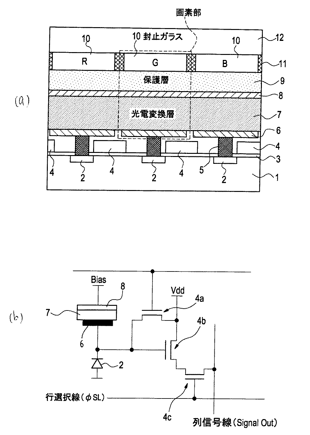
以下、本発明の実施形態を説明するための固体撮像素子について図面を参照して説明する。この固体撮像素子は、デジタルカメラやデジタルビデオカメラ等の撮像装置に搭載して用いられるものである。 Hereinafter, a solid-state imaging device for describing an embodiment of the present invention will be described with reference to the drawings. This solid-state imaging device is used by being mounted on an imaging device such as a digital camera or a digital video camera.
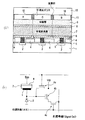
図1(a)は、本発明の実施形態を説明するための固体撮像素子の概略構成を示す断面模式図である。図1(a)に示す固体撮像素子は、基板の一例であるp型シリコン基板1上方に2次元状(例えば正方格子状)又は1次元状に配列された例えば四角形状の多数の画素部を備える。図1(a)では、所定方向に並ぶ3つの画素部の断面を示している。
FIG. 1A is a schematic cross-sectional view showing a schematic configuration of a solid-state imaging device for explaining an embodiment of the present invention. The solid-state imaging device shown in FIG. 1A includes a large number of pixel portions, for example, a square shape arranged in a two-dimensional shape (for example, a square lattice shape) or a one-dimensional shape above a p-
各画素部は、p型シリコン基板1上方に設けられた下部電極6、下部電極6上方に設けられた上部電極8、及び下部電極6と上部電極8の間に設けられた光電変換層7を含む光電変換部と、上部電極8上に設けられた保護層9と、保護層9上に設けられたカラーフィルタ10とを備える。
Each pixel portion includes a
下部電極6は、アルミニウムやチタンナイトライド等の入射光に対して不透明な電極であり、画素部毎に分離されている。カラーフィルタ10の中心と下部電極6の中心とは平面視において一致している。
The
光電変換層7は、可視域の光を吸収し、吸収した光に応じた信号電荷を発生する光電変換材料で構成されている。この光電変換材料としては、公知の有機又は無機の材料を用いることができる。光電変換層7は、全ての画素部で共通の一枚構成となっているが、画素部毎に分離した構成としても良い。 The photoelectric conversion layer 7 is made of a photoelectric conversion material that absorbs visible light and generates signal charges corresponding to the absorbed light. As this photoelectric conversion material, a known organic or inorganic material can be used. The photoelectric conversion layer 7 has a single configuration common to all the pixel units, but may be configured to be separated for each pixel unit.
上部電極8は、ITO等の入射光に対して透明な電極であり、全ての画素部で共通の一枚構成となっている。上部電極8は、画素部毎に分離した構成としても良い。上部電極8には、光電変換層7に電界をかけられるように、所定のバイアス電圧が印加可能となっている。 The upper electrode 8 is an electrode that is transparent to incident light, such as ITO, and has a single configuration common to all the pixel portions. The upper electrode 8 may be separated for each pixel portion. A predetermined bias voltage can be applied to the upper electrode 8 so that an electric field can be applied to the photoelectric conversion layer 7.
保護層9は、光電変換部を保護するためのものであり、入射光に対して透明な絶縁材料等で構成されている。光電変換層7を有機材料で形成する場合、有機材料は一般に水や溶剤による特性劣化が大きく、フォトリソグラフィ法に不向きである。しかし、カラーフィルタ10形成時にはフォトリソグラフィ法が一般的に用いられるため、保護層9を設けないと、光電変換層7の特性劣化が懸念される。そこで、図1(a)に示す固体撮像素子では光電変換層7とカラーフィルタ10との間に保護層9を設けている。保護層9は、例えばアルミナ膜や窒化膜を用いることができる。
The
カラーフィルタ10には、赤色(R)の波長域の光を透過するRカラーフィルタと、緑色(G)の波長域の光を透過するGカラーフィルタと、青色(B)の波長域の光を透過するBカラーフィルタとの3種類が含まれる。多数の画素部は、Rカラーフィルタを含む画素部と、Gカラーフィルタを含む画素部と、Bカラーフィルタを含む画素部で構成されており、カラー画像を生成できるように、各画素部が所定のパターンで配置されている。
The
p型シリコン基板1内には、画素部に対応させて高濃度のn型不純物層からなる電荷蓄積部2が形成されている。電荷蓄積部2は、対応する画素部の光電変換層7で発生した信号電荷を蓄積するものであり、タングステン等の導電性材料のプラグ5を介して、対応する画素部の下部電極6と電気的に接続されている。
In the p-
p型シリコン基板1には、更に、電荷蓄積部2に対応させて信号読み出し回路4が形成されている。信号読み出し回路4は、対応する電荷蓄積部2に蓄積された信号電荷に応じた電圧信号を出力するためのものであり、CMOS回路やCCDとアンプを用いた回路等を用いることができる。
A
図1(b)は、図1(a)に示す信号読み出し回路4の構成例を示した図である。
図1(b)に示すように、信号読み出し回路4は、電荷蓄積部2に蓄積された信号電荷をリセットするためのリセットトランジスタ4aと、電荷蓄積部2に蓄積された信号電荷を電圧信号に変換するための出力トランジスタ4bと、出力トランジスタ4bから出力された電圧信号を列信号線に出力するための選択トランジスタ4cとを備えた公知の3トランジスタ構成となっている。p型シリコン基板1上には、これらトランジスタのゲート酸化膜3が形成されている。ゲート酸化膜3は例えば酸化シリコンで構成されている。
FIG. 1B is a diagram illustrating a configuration example of the
As shown in FIG. 1B, the
図1(a)に示す固体撮像素子は、任意の画素部のカラーフィルタ10に入射した光が該画素部の隣の画素部に入射するのを防止するための隔壁11を備える。隔壁11は、隣接する画素部のカラーフィルタ10同士の間に、カラーフィルタ10の側面を覆って設けられている。
The solid-state imaging device shown in FIG. 1A includes a
隔壁11は、入射光を吸収又は反射する領域であれば良く、入射光を吸収又は反射する材料(例えばタングステンやアルミニウム等の金属、黒色の染料や顔料等)で構成したり、入射光を全反射する空気層で構成したりすることができる。空気層で入射光を全反射させるには、画素部のカラーフィルタ10への入射光の入射角をαとし、空気層の屈折率をnとすると、「sin(90°−α)>(1/n)」の条件を満たせば良い。例えば、n=1.5とすると、α<48.2°で条件を満たすため、ほとんどの斜め光を全反射させることができる。
The
カラーフィルタ10及び隔壁11の上には固体撮像素子全体を封止する封止ガラス12が設けられている。
A sealing
以上のように構成された固体撮像素子の動作について説明する。 The operation of the solid-state imaging device configured as described above will be described.
入射光のうちのR光はRカラーフィルタ10を透過し、Rカラーフィルタ10下方の光電変換層7に入射し、ここでR光に応じた信号電荷が発生する。入射光のうちのG光はGカラーフィルタ10を透過し、Gカラーフィルタ10下方の光電変換層7に入射し、ここでG光に応じた信号電荷が発生する。入射光のうちのB光はBカラーフィルタ10を透過し、Bカラーフィルタ10下方の光電変換層7に入射し、ここでB光に応じた信号電荷が発生する。各カラーフィルタ10に斜めに入射してきた光は、その一部がカラーフィルタ10の側面を覆う隔壁11によって吸収又は反射されるため、隣の画素部に到達してしまう光は減少する。
Of the incident light, the R light passes through the
各光電変換層7で発生した信号電荷は、そこに加わる電界によって下部電極6に集められ、ここからプラグ5を介して電荷蓄積部2に移動し、ここで蓄積される。蓄積された信号電荷は、信号読み出し回路4によって電圧信号として列信号線に順次出力される。固体撮像素子から出力された電圧信号に所定の信号処理を施すことで、カラー画像データを生成することができる。
The signal charge generated in each photoelectric conversion layer 7 is collected by the
以上のように、図1(a)に示した固体撮像素子によれば、カラーフィルタ10同士の間に隔壁11が設けられているため、任意の画素部のカラーフィルタ10に入射してきた光が該画素部の隣の画素部に入射してしまう確率を減らすことができる。このため、混色を低減することができ、高画質撮像が可能な固体撮像素子を実現することができる。画素部のサイズが2μm以下になると、光電変換層7の下面からカラーフィルタ10の上面までの厚みと、画素部のサイズが同程度となり、斜め入射光が隣の画素部に漏れこみやすくなる。そこで、隔壁11を設けて、斜め入射光が隣の画素部に漏れこむ確率を減らすことで、微細化が進んだ場合でも、画質を維持することが可能となる。
As described above, according to the solid-state imaging device illustrated in FIG. 1A, the
隔壁11は、Rカラーフィルタ、Gカラーフィルタ、Bカラーフィルタを保護層9上に順に形成後、カラーフィルタ10同士の境界部分に開口を形成し、この開口に光を反射又は吸収する材料を埋めたり、開口内に何も埋めないまま封止ガラス12を形成したりすることで形成することができる。または、光を反射又は吸収する材料によって保護層9上に隔壁11を形成した後、隔壁11で囲まれた空間内にカラーフィルタ10を埋め込む方法を採用しても良い。これらの製造方法を採用することで、異なる色のカラーフィルタ10が境界部分でオーバーラップしてしまうのを防ぐことができるため、混色を更に防止することが可能となる。また、隔壁11を空気層で形成した場合は、製造工程を簡略化することができるため、製造コストを削減することができる。
The
なお、図1(a)に示した固体撮像素子では、保護層9の厚みが0より大きく1.0μm以下であれば、混色を実用上問題ないレベルまで低減できることが分かった。また、隔壁11のカラーフィルタ10表面に平行な方向の幅が、0.05μm以上で且つ画素部のサイズの0.2倍以下であり、更に、カラーフィルタ10と保護層9の厚みの合計が0.2μm以上1.4μm以下であれば、光利用率を実用上問題ないレベルにまで低減することができることが分かった。
In the solid-state imaging device shown in FIG. 1A, it has been found that if the thickness of the
画素部のサイズとは、図2に示すように、カラーフィルタ10を正方形としたとき、(隣接するカラーフィルタ10同士の間の隔壁11の幅の1/2)+(カラーフィルタ10の1辺の長さ)+(隣接するカラーフィルタ10同士の間の隔壁11の幅の1/2)で定義される。以下では、これらの数値の根拠をシミュレーションによって得た結果により説明する。
As shown in FIG. 2, when the
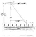
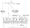
図3は、シミュレーションした撮像装置の構成を示した図である。図3に示す撮像装置は、図1に示した固体撮像素子と、撮像レンズ20とを備える。本シミュレーションでは、固体撮像素子の封止ガラス12を省略している。
FIG. 3 is a diagram illustrating a configuration of a simulated imaging apparatus. The imaging device shown in FIG. 3 includes the solid-state imaging device shown in FIG. In this simulation, the sealing
図4は、図3に示す撮像装置にxy座標を設定した図である。撮像レンズ20の光軸をy軸、光軸と直交する方向をx軸とし、光軸上の撮像レンズ20の射出瞳の中心位置を(0,L)、光軸上のカラーフィルタ10上面位置を(0,0)、光軸上の保護層9上面位置を(0,−Tf)、光軸上の光電変換層7のy軸方向の中央位置を(0,−Tf−Tp−To/2)とする。
FIG. 4 is a diagram in which xy coordinates are set in the imaging apparatus shown in FIG. The optical axis of the
なお、光電変換層7に入射した光線は、光電変換層7の上部電極8と下部電極6とで挟まれる領域のy軸方向の中央位置で100%光電変換されるものと仮定する。さらに、上部電極8は数nmと非常に薄いのでシミュレーションでは無視する。
It is assumed that the light incident on the photoelectric conversion layer 7 is 100% photoelectrically converted at the center position in the y-axis direction of the region sandwiched between the upper electrode 8 and the
また、撮像レンズ20のx軸方向の径をDとする。撮像レンズ20の光軸、つまり固体撮像素子の中心から任意の画素部の中心までの距離(画素シフト量)をPSとする。画素部サイズをPpとする。隔壁11のx軸方向の幅をKとする。下部電極6のx軸方向の幅をPaとする。撮像レンズ20の射出瞳面の座標を(x1,L)、カラーフィルタ10表面の座標を(x2,0)、保護層9表面の座標を(x3,−Tf)、光電変換層7のy軸方向中央の座標を(x4,−Tf−Tp−To/2)とする。
The diameter of the
このような設定により、撮像レンズ20の左端の座標は(−D/2,L)となり、右端の座標は(D/2,L)となる。任意の画素部の左端の座標は(PS−Pp/2,0)となり、右端の座標は(PS+Pp/2,0)となる。
With this setting, the left end coordinate of the
任意の画素部のカラーフィルタ10上面の左端の座標は(PS−Pp/2+K/2,0)となり、右端の座標は(PS+Pp/2−K/2,0)となる。任意の画素部のカラーフィルタ10下面の左端の座標は(PS−Pp/2+K/2,−Tf)となり、右端の座標は(PS+Pp/2−K/2,−Tf)となる。
The coordinates of the left end of the upper surface of the
下部電極6の左端上方の光電変換層7中央の座標は(PS−Pa/2,−Tf−Tp−To/2)となり、右端上方の光電変換層7中央の座標は(PS+Pa/2,−Tf−Tp−To/2)となる。
The coordinates of the center of the photoelectric conversion layer 7 above the left end of the
カラーフィルタ10、保護層9、上部電極8、光電変換層7の屈折率をそれぞれnとし、カラーフィルタ10に入射する光線の入射角をα、屈折角をβとする。
The refractive indexes of the
以下、このような設定のもと行った光線追跡法のシミュレーションの手順を説明する。 Hereinafter, the simulation procedure of the ray tracing method performed under such setting will be described.
1)撮像レンズ20の射出瞳面の点A(x1,L)から画素部最上面(カラーフィルタ10表面)の点B(x2,0)に光線が入射したとする。点ABを通る直線は以下の一般式(1)で示される。
1) It is assumed that a light ray is incident on a point B (x2, 0) on the uppermost surface of the pixel portion (the surface of the color filter 10) from a point A (x1, L) on the exit pupil plane of the
y1=L、y2=0より、上記式は以下の直線の式(2)で示される。 From y1 = L and y2 = 0, the above equation is expressed by the following linear equation (2).
2)次に、点B(x2,0)に入射した光線は、画素部最上面で屈折するため、屈折後の直線の式を求める。 2) Next, since the light beam incident on the point B (x2, 0) is refracted at the uppermost surface of the pixel portion, the equation of the straight line after refraction is obtained.
であるので、点B(x2,0)を通り、傾き1/tanβの直線(屈折後の直線)の式は、下記式(3)で示される。 Therefore, an equation of a straight line (a straight line after refraction) passing through the point B (x2, 0) and having an inclination of 1 / tan β is expressed by the following equation (3).
屈折後の直線と保護層9表面(x3面)との交点は、式(3)においてx=x3、y=−Tfであるため、
“x3=−Tf・tanβ+x2”となる。
Since the intersection of the straight line after refraction and the surface of the protective layer 9 (x3 plane) is x = x3 and y = −Tf in the equation (3),
“X3 = −Tf · tan β + x2”.
また、屈折後の直線と光電変換層7の中央(x4面)との交点は、式(3)においてx=x4、y=−Tf−Tp−To/2であるため、
“x4=−(Tf+Tp+To/2)tanβ+x2”となる。
Moreover, since the intersection of the straight line after refraction and the center (x4 surface) of the photoelectric conversion layer 7 is x = x4 and y = −Tf−Tp−To / 2 in the equation (3),
“X4 = − (Tf + Tp + To / 2) tan β + x2”.
3)撮像レンズ20の射出瞳面上の左端(−D/2,L)から、カラーフィルタ10表面上の画素シフト量PSの画素部の左端(PS−Pp/2,0)から右端(PS+Pp/2,0)までdpピッチでN本の光線を引き、更に、各光線の屈折後の光線が、x2面、x3面、x4面で
(PS−Pp/2+K/2,0)から(PS+Pp/2−K/2,0)の範囲
(PS−Pp/2+K/2,−Tf)から(PS+Pp/2−K/2,−Tf)の範囲
(PS−Pa/2,−Tf−Tp−To/2)から(PS+Pa/2,−Tf−Tp−To/2)の範囲
を満たす光線の本数を数える。
3) From the left end (−D / 2, L) on the exit pupil plane of the
4)撮像レンズ20の射出瞳面上の光線射出位置を左端から右端までdDピッチで移動させながら上記計算を繰り返す。
4) The above calculation is repeated while moving the light beam emission position on the exit pupil plane of the
5)全光線数をTN、撮像レンズ20の射出瞳中心(0,L)からカラーフィルタ10表面上の中心(PS,0)への光束の入射角をθ(tanθ=PS/L)とし、入射角θで該カラーフィルタ10を含む画素部内の下部電極6上の光電変換層7の中央面に到達した光線数をPl(θ)、入射角θで該画素部の隣りの画素部の下部電極6上の光電変換層7の中央面に到達した光線数をPc(θ)とすると、2次元面での光利用効率及び混色率は、
2次元光利用率Ql(θ)=Pl(θ)/TN
2次元混色率Qc(θ)=Pc(θ)/TN
となる。
5) The total number of rays is TN, the incident angle of the light beam from the exit pupil center (0, L) of the
Two-dimensional light utilization factor Ql (θ) = Pl (θ) / TN
Two-dimensional color mixing ratio Qc (θ) = Pc (θ) / TN
It becomes.
6)以上の計算を、カラーフィルタ10表面上の画素シフト量PSを増加(θを増加)させながら繰り返す。 6) The above calculation is repeated while increasing the pixel shift amount PS on the surface of the color filter 10 (increasing θ).
7)さらに、3次元空間での光利用効率及び混色率を、入射角θ=0(PS=0)での光利用率Ql(0)を用い次式で近似した。この場合、レンズ瞳を矩形と近似した場合と一致する。
光利用率Sl(θ)=Ql(θ)・Ql(0)
混色率Sc(θ)=Qc(θ)・Ql(0)
7) Further, the light utilization efficiency and the color mixing ratio in the three-dimensional space were approximated by the following equations using the light utilization ratio Ql (0) at the incident angle θ = 0 (PS = 0). In this case, this is the same as when the lens pupil is approximated to a rectangle.
Light utilization rate Sl (θ) = Ql (θ) · Ql (0)
Color mixing ratio Sc (θ) = Qc (θ) · Ql (0)
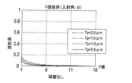
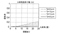
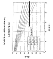
デジタルカメラ、ビデオカメラ、携帯モジュール等に用いる固体撮像素子においては、撮像レンズ20の絞りを変化させた時の撮像特性変化(F値依存)と、撮像画像の中心と周辺、即ち撮像レンズ20の射出瞳から固体撮像素子への光束の入射角の違いによる撮像特性変化(入射角依存)が許容値以内であることが重要となる。そこで、画素部サイズ、カラーフィルタ10の厚さ、保護層9の厚さをパラメータにして、F値依存と入射角依存を考察した。その結果を以下に示す。
In a solid-state imaging device used for a digital camera, a video camera, a portable module, etc., an imaging characteristic change (F value dependency) when the aperture of the
A)隔壁11が有る場合と無い場合の特性の違い
画素部サイズ:2μm、カラーフィルタ10厚さTf:1μm、保護層9厚さTp:可変として、隔壁11有無でのF値依存と入射角依存のシミュレーション結果を図5〜図12に示す。隔壁11なしとは、即ち、上記Kの値がゼロであることを意味する。
A) Difference in characteristics with and without the
図5は、図3の構成において隔壁11なしのときの光利用率のF値依存特性のシミュレーション結果を示す図である。図6は、図3の構成において隔壁11ありのときの光利用率のF値依存特性のシミュレーション結果を示す図である。図7は、図3の構成において隔壁11なしのときの光利用率の入射角依存特性のシミュレーション結果を示す図である。図8は、図3の構成において隔壁11ありのときの光利用率の入射角依存特性のシミュレーション結果を示す図である。
FIG. 5 is a diagram showing a simulation result of the F value dependency characteristic of the light utilization rate when the
図9は、図3の構成において隔壁11なしのときの混色率のF値依存特性のシミュレーション結果を示す図である。図10は、図3の構成において隔壁11ありのときの混色率のF値依存特性のシミュレーション結果を示す図である。図11は、図3の構成において隔壁11なしのときの混色率の入射角依存特性のシミュレーション結果を示す図である。図12は、図3の構成において隔壁11ありのときの混色率の入射角依存特性のシミュレーション結果を示す図である。
FIG. 9 is a diagram showing a simulation result of the F-number dependency characteristic of the color mixture rate when the
上記結果より、
・隔壁11を用いることで光利用率には大差ないが混色率は大幅に低減される。
・混色率は、保護層9厚さTpに依存する。
・任意のF値と入射角で混色率が低くなる条件は、全てのF値と入射角で混色率が低くなる。
ことが分かった。次に、隔壁11ありについて、F値:5.6、入射角:25度における、光利用率及び混色率と、カラーフィルタ10厚さTf、保護層9厚さTp、画素部サイズPpの関係を考察した。その結果を以下に示す。
From the above results,
-By using the
The color mixing ratio depends on the
The condition that the color mixing rate is low at an arbitrary F value and incident angle is that the color mixing rate is low at all F values and incident angles.
I understood that. Next, with the
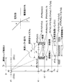
B)光利用率及び混色率と、カラーフィルタ10厚さTf、保護層9厚さTp、画素部サイズPpの関係
(a)保護層9厚さTp=1μmに固定し、カラーフィルタ10厚さTfを変化させた場合
図13は、図3の構成において保護層9厚さTp=1μmに固定し、カラーフィルタ10厚さTfを変化させた場合の光利用率のシミュレーション結果を示す図である。図14は、図3の構成において保護層9厚さTp=1μmに固定し、カラーフィルタ10厚さTfを変化させた場合の混色率のシミュレーション結果を示す図である。
B) Relationship between light utilization rate and color mixture rate,
(b)カラーフィルタ10厚さTf=1μmに固定し、保護層9厚さTpを変化させた場合
図15は、図3の構成においてカラーフィルタ10厚さTf=1μmに固定し、保護層9厚さTpを変化させた場合の光利用率のシミュレーション結果を示す図である。図16は、図3の構成においてカラーフィルタ10厚さTf=1μmに固定し、保護層9厚さTpを変化させた場合の混色率のシミュレーション結果を示す図である。
(B) When
(c)Tf+Tp=2μmに固定し、保護層9厚さTpを変化させた場合
図17は、図3の構成においてTf+Tp=2μmに固定し、保護層9厚さTpを変化させた場合の光利用率のシミュレーション結果を示す図である。図18は、図3の構成においてTf+Tp=2μmに固定し、保護層9厚さTpを変化させた場合の混色率のシミュレーション結果を示す図である。
(C) In the case where Tf + Tp = 2 μm is fixed and the thickness Tp of the
(d)保護層9厚さTp=0.4μmに固定してTf+Tpを変化させた場合
図19は、図3の構成において保護層9厚さTp=0.4μmに固定してTf+Tpを変化させた場合の光利用率のシミュレーション結果を示す図である。図20は、図3の構成において保護層9厚さTp=0.4μmに固定してTf+Tpを変化させた場合の混色率のシミュレーション結果を示す図である。
(D) When the
上記結果より、
・保護層9厚さTpが一定ならカラーフィルタ10厚さTfが変化しても混色率はあまり変化しない。
・Tf+Tpが一定なら保護層9厚さTpが変化しても光利用率はあまり変化しない。
ことが分かり、この結果、混色率の特性はTpで規定でき、光利用率の特性はTf+Tpで規定できることが分かった。
From the above results,
If the thickness Tp of the
-If Tf + Tp is constant, the light utilization rate does not change much even if the thickness Tp of the
As a result, it was found that the color mixing rate characteristic can be defined by Tp, and the light utilization factor characteristic can be defined by Tf + Tp.
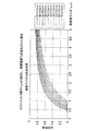
次に、固体撮像素子として許容できる混色率を実現できるTpの値、固体撮像素子として許容できる光利用率を実現できるTf+Tpの値を調べた。 Next, the value of Tp that can realize an acceptable color mixing ratio as a solid-state image sensor and the value of Tf + Tp that can realize an acceptable light utilization rate as a solid-state image sensor were examined.
図21は、図3の構成において保護層9厚さTpを変化させた場合の混色率のシミュレーション結果を示す図である。ここで、混色率は、入射角25度、F値5.6、画素部サイズ1μm以上の条件で20%以下が許容できると仮定する。この仮定は、従来の固体撮像素子の特性と比較して当業者にとっては適切な仮定である。図21に示すシミュレーション結果から、保護層9厚さTpが1.0μm以下、好ましくは0.4μm以上1.0μm以下であれば、混色率は許容されることが分かった。なお、保護層9の厚さの下限値は0より大きい。したがって、保護層9の厚さは、0より大きく1.0μm以下であることが望ましい。
FIG. 21 is a diagram showing a simulation result of the color mixture rate when the thickness Tp of the
図22は、図3の構成においてTf+Tpを変化させた場合の光利用率のシミュレーション結果を示す図である。ここで、光利用率は、入射角25度、F値5.6、画素部サイズ1μm以上の条件での光利用率が、入射角0度、F値5.6、画素部サイズ1μm以上の条件での光利用率の50%以上となるときを許容できると仮定する。この仮定は、従来の固体撮像素子の特性と比較して当業者にとっては適切な仮定である。図22に示すシミュレーション結果から、Tf+Tpが1.4μm以下であれば、光利用率は許容されることが分かった。なお、カラーフィルタ10の厚さは、カラーフィルタを構成する顔料や染料の吸光度、バインダーへの分散率と、所望する分光透過率特性で決まるが、概ね0.2μm以上が必要となる。したがって、Tf+Tpは、0.2μmより大きく1.4μm以下であることが望ましい。
FIG. 22 is a diagram showing a simulation result of the light utilization rate when Tf + Tp is changed in the configuration of FIG. Here, the light utilization factor is an incident angle of 25 degrees, an F value of 5.6, and a pixel unit size of 1 μm or more. The light utilization factor is an incident angle of 0 degree, an F value of 5.6, and a pixel unit size of 1 μm or more. It is assumed that the case where the light utilization rate under the condition is 50% or more is acceptable. This assumption is an appropriate assumption for those skilled in the art as compared with the characteristics of the conventional solid-state imaging device. From the simulation results shown in FIG. 22, it was found that the light utilization rate is acceptable if Tf + Tp is 1.4 μm or less. The thickness of the
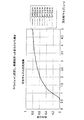
本シミュレーションの固体撮像素子は、隔壁11を有しているが、隔壁11はその幅Kが小さいほど、画素部における隔壁11の占める割合が減るため、画素部の開口率が大きくなる。開口率が大きくなれば、光利用率も向上する。図23は、図3の構成において画素部サイズ2μm、F値16、隔壁幅K:可変における光利用率の入射角依存特性のシミュレーション結果を示す図である。
The solid-state imaging device of this simulation has the
実用上、光利用率は、入射角0度で0.6以上が望ましいとすると、図23に示す結果から、隔壁幅Kは0.4μm以下、つまり、画素部サイズに占める隔壁11の幅Kの割合は0.2以下である必要がある。一方、隔壁幅Kの下限値は、それを構成する材料で決まり、隔壁11が入射光を充分に吸収又は反射するためには、例えばチタンブラックが分散されたレジストの場合で0.2μm以上、金属の場合で0.05μm以上の幅が必要となる。したがって、隔壁幅Kは、0.05μm以上で且つ画素部サイズの0.2倍以下であることが望ましい。
Assuming that the light utilization factor is practically 0.6 or more at an incident angle of 0 degree, from the result shown in FIG. 23, the partition wall width K is 0.4 μm or less, that is, the width K of the
以下、図1に示した固体撮像素子の別の構成例について説明する。 Hereinafter, another configuration example of the solid-state imaging device illustrated in FIG. 1 will be described.
図24は、図1に示した固体撮像素子の別の構成例の固体撮像素子を搭載した撮像装置の概略構成を示した図である。図24では、固体撮像素子の下部電極6より下の構成要素の図示を省略している。また、図3と同じ構成には同一符号を付してある。
FIG. 24 is a diagram illustrating a schematic configuration of an imaging apparatus in which the solid-state imaging device of another configuration example of the solid-state imaging device illustrated in FIG. 1 is mounted. In FIG. 24, illustration of components below the
図24に示す撮像装置の固体撮像素子は、各画素部のカラーフィルタ10に対する下部電極6の位置が、固体撮像素子の中心から周辺に向かうにしたがって周辺側にずれていることが図1に示す固体撮像素子と異なる点である。
24 shows that the position of the
図24に示すように、中央に光軸が通る画素部以外の各画素部では、カラーフィルタ10の中心を通る光線が、光電変換層7の下部電極6と上部電極8で挟まれる領域の中心に到達するように、下部電極6の中心が、カラーフィルタ10の中心よりもΔPだけ周辺側にずれている。
As shown in FIG. 24, in each pixel portion other than the pixel portion where the optical axis passes through the center, the center of the region where the light beam passing through the center of the
周辺の画素部では、入射光の入射角度が大きくなるため、カラーフィルタ10の中心と下部電極6の中心とが重なっている中央の画素部と周辺の画素部とが同じ構成では、周辺の画素部で検出できる光量が相対的に少なくなって輝度シェーディングが発生したり、画素部に入射した光が該画素部の隣の画素部に入射しやすくなって色シェーディングが発生したりする。
Since the incident angle of incident light is large in the peripheral pixel portion, the peripheral pixel portion is the same when the central pixel portion where the center of the
図24に示した構成によれば、各画素部において光を検出する領域(光電変換層7の下部電極6と上部電極8とで挟まれる領域)を周辺に行くにしたがって周辺側にずらしている(このことを画素ずらしとも言う)ため、周辺での光量不足を回避することができる。この結果、輝度シェーディングや色シェーディングを抑制することができる。
According to the configuration shown in FIG. 24, the region for detecting light in each pixel unit (the region sandwiched between the
フォトダイオードが形成された半導体基板上方にカラーフィルタを設けた一般的な固体撮像素子では、中心から周辺に向かうにしたがってカラーフィルタ及びフォトダイオードを周辺側にずらすことで、色シェーディングや輝度シェーディングを抑制することが従来行われている。しかし、このような一般的な固体撮像素子では、カラーフィルタ中心を通った光線がフォトダイオード表面の中心に到達するようにしており、図24に示した構成とは異なる。図24に示した構成によれば、光電変換層7の中心にカラーフィルタ中心を通った光線が到達するようにしているため、光利用率を良くすることができ、混色率を低くすることができる。 In general solid-state image sensors with a color filter above the semiconductor substrate on which the photodiode is formed, color shading and luminance shading are suppressed by shifting the color filter and photodiode toward the peripheral side from the center toward the periphery. It has been done conventionally. However, in such a general solid-state imaging device, the light beam that passes through the center of the color filter reaches the center of the photodiode surface, which is different from the configuration shown in FIG. According to the configuration shown in FIG. 24, since the light beam that has passed through the center of the color filter reaches the center of the photoelectric conversion layer 7, the light utilization rate can be improved and the color mixing rate can be reduced. it can.
以下、上述した画素ずらし量ΔPの好ましい値について考察する。 Hereinafter, a preferable value of the above-described pixel shift amount ΔP will be considered.
図24に示す撮像装置において、撮像レンズ20の射出瞳位置と固体撮像素子との距離をL、撮像レンズ20の射出瞳中心を出て各カラーフィルタ10の中心を通り、下部電極6上の光電変換層7中心に到達する任意の光線が固体撮像素子に入射する時の入射点と光軸との距離をP、該光線の入射角をα、該光線の屈折角をβ、カラーフィルタ10の中心と光電変換層7の中心との光軸方向の距離をT、封止ガラス12、カラーフィルタ10、保護層9、上部電極8、及び光電変換層7の屈折率をnとすると次式(4)が成立つ。
In the imaging apparatus shown in FIG. 24, the distance between the exit pupil position of the
例えば、L=500μm、α=25°、T(カラーフィルタ10の光軸方向の厚さの1/2+保護層9の光軸方向の厚さ+光電変換層7の光軸方向の厚さの1/2)=1.65μm、屈折率n=1.5とすると、P=233μm、β=16.36°、ΔP=0.484μmとなる。したがって、中心から任意の画素部までの距離に対する当該画素部における画素ずらし量の比率は、ΔP/P≒0.002が理想的となる。
For example, L = 500 μm, α = 25 °, T (1/2 of the thickness of the
次に、ΔP/P≒0.002としたときの混色率及び光利用効率を、上述した光線追跡法によるシミュレーションで求めた。なお、このシミュレーションでは、固体撮像素子が封止ガラス12を有する構成であるため、封止ガラス12の光軸方向の厚みをGとし、封止ガラス12表面の座標を(x5,G)とし、この面に入射してきた光線の屈折後の光線の軌跡を前述したように求めることで、混色率及び光利用効率を求めた。
Next, the color mixing ratio and the light utilization efficiency when ΔP / P≈0.002 were obtained by the simulation using the ray tracing method described above. In this simulation, since the solid-state imaging device has the sealing
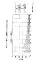
まず、撮像レンズ20のF値:5.6、L:500μm、画素部サイズPp:2μm、隔壁11の幅K:0.1μm、カラーフィルタ10の光軸方向の厚さTf:1μm、保護層9の光軸方向の厚さTp:1μm、光電変換層9の光軸方向の厚さTo:0.3μm、下部電極6の幅Pa:1.9μmの条件で、隔壁11で挟まれたカラーフィルタ10と下部電極6の位置関係を、下部電極6の方が固体撮像素子の周辺に向かって外側に、カラーフィルタ10の中心位置からΔP=0.002Pずらした場合と、下部電極6をずらさない場合とをシミュレーションし、それぞれについて混色率及び光利用率を求めた。
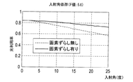
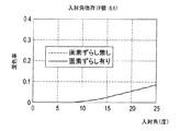
First, the F value of the imaging lens 20: 5.6, L: 500 μm, the pixel part size Pp: 2 μm, the width K of the partition wall 11: 0.1 μm, the thickness Tf of the
図25は、図24に示した構成において、画素ずらしを行った場合と画素ずらしを行わない場合の光利用率のシミュレーション結果を示した図である。図26は、図24に示した構成において、画素ずらしを行った場合と画素ずらしを行わない場合の混色率のシミュレーション結果を示した図である。 FIG. 25 is a diagram illustrating a simulation result of the light utilization rate when the pixel shift is performed and when the pixel shift is not performed in the configuration illustrated in FIG. FIG. 26 is a diagram illustrating a simulation result of the color mixture rate when the pixel shift is performed and when the pixel shift is not performed in the configuration illustrated in FIG.
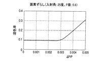
図25に示すように、画素ずらしを行うことにより、輝度シェーディング(入射角の増加にともなって光利用率低下)は明らかに改善される。一方、色シェーディング(入射角の増加にともなって混色増加)は、画素ずらしの有無によってほとんど差異が見られない。これは、今回の条件では、隔壁11が既に混色を抑圧している結果だと考えられる。
As shown in FIG. 25, luminance shading (decrease in the light utilization rate as the incident angle increases) is clearly improved by performing pixel shifting. On the other hand, there is almost no difference in color shading (increase in color mixture as the incident angle increases) depending on the presence or absence of pixel shift. This is considered to be a result of the
次に、同条件で、ΔP/Pを変化させた時の入射角25度に対する光利用率変化と混色率変化を求めた。結果を図27及び図28に示す。 Next, under the same conditions, the change in the light utilization rate and the change in the color mixture rate with respect to the incident angle of 25 degrees when ΔP / P was changed were obtained. The results are shown in FIGS.
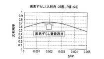
図27及び図28より、ΔP/Pが0.001〜0.0032の範囲で、入射角25度に対する光利用率が最大、混色率が最少、即ち、輝度シェーディング最少、色シェーディング最少となることが分かった。 27 and 28, ΔP / P is in the range of 0.001 to 0.0032, the light utilization rate for the incident angle of 25 degrees is the maximum, the color mixture rate is the minimum, that is, the luminance shading is minimum and the color shading is minimum. I understood.
なお、式(4)より From equation (4)
であるので、n=1.5とすると、ΔP/P=0.667T/Lとなる。 Therefore, if n = 1.5, ΔP / P = 0.667 T / L.
一方、L=500μm、T=1.65μm、n=1.5、入射角25°の場合について、シミュレーションすると、図27より、光利用率については、ΔP/P=0.001から0.0032が、最適点から約5%ダウン以内(ほぼ最適点と同じ)となる。また、図28より、混色率は、ΔP/P=0〜0.003で最適点からは変化がない。 On the other hand, simulation is performed for the case of L = 500 μm, T = 1.65 μm, n = 1.5, and an incident angle of 25 °, and from FIG. 27, the light utilization factor is ΔP / P = 0.001 to 0.0032. However, it is within about 5% down from the optimum point (substantially the same as the optimum point). Further, as shown in FIG. 28, the color mixture ratio is ΔP / P = 0 to 0.003, and there is no change from the optimum point.
ここで、図27、図28は、横軸がΔP/Pで標記されているが、L=500μm、T=1.65μm、つまりT/L=0.0033の場合なので、ΔP/P=0.001≒0.303T/L、ΔP/P=0.0032≒0.97T/L、ΔP/P=0=0×T/L、ΔP/P=0.003≒0.909T/Lと変換できる。 Here, in FIGS. 27 and 28, the horizontal axis is indicated by ΔP / P, but since L = 500 μm and T = 1.65 μm, that is, T / L = 0.0005, ΔP / P = 0. .001≈0.303 T / L, ΔP / P = 0.002≈0.97 T / L, ΔP / P = 0 = 0 × T / L, ΔP / P = 0.003≈0.909 T / L it can.
以上、上記ΔP/Pの変換式とシミュレーション結果を鑑み、{ΔP(任意の画素部のカラーフィルタ10の中心と下部電極6の中心とのずれ量)÷P(任意の画素部のカラーフィルタ10の中心を通る光線と固体撮像素子表面(封止ガラス12表面)との交点から、固体撮像素子表面と光軸との交点までの距離)}を、0.303T/L以上0.909T/L以下とすることが望ましい。
In view of the above ΔP / P conversion formula and simulation results, {ΔP (the amount of deviation between the center of the
なお、図1に示した固体撮像素子や図24に示した固体撮像素子の各画素部のカラーフィルタ10上に、光電変換層7に光を集光するためのマイクロレンズを設けた構成としても良い。マイクロレンズを設けることにより、画素部間の光漏れを更に抑制して、色シェーディングや輝度シェーディングを抑制することができる。
Note that a microlens for condensing light on the photoelectric conversion layer 7 may be provided on the
1 p型シリコン基板
6 下部電極
7 光電変換層
8 上部電極
9 保護層
10 カラーフィルタ
11 隔壁
1 p-
Claims (10)
前記画素部が、前記基板上方に設けられた光電変換部と、前記光電変換部上方に設けられたカラーフィルタとを含み、
前記画素部の前記カラーフィルタに入射した光が隣の前記画素部に入射するのを防止するための隔壁を備え、
前記隔壁が、隣接する前記画素部の前記カラーフィルタ同士の間に前記カラーフィルタの側面を覆って設けられており、
前記光電変換部が、前記基板上方に設けられた下部電極、前記下部電極上方に設けられた上部電極、及び前記下部電極と前記上部電極の間に設けられた光電変換層を含み、
前記画素部が、前記カラーフィルタと前記上部電極との間に設けられた、前記光電変換部を保護するための保護層を含み、
前記保護層の厚さが、0より大きく1.0μm以下である固体撮像素子。 A solid-state imaging device having a large number of pixel portions arranged above a substrate,
The pixel unit includes a photoelectric conversion unit provided above the substrate, and a color filter provided above the photoelectric conversion unit,
A partition for preventing light incident on the color filter of the pixel unit from entering the adjacent pixel unit;
The partition is provided between the color filters of the adjacent pixel portions so as to cover the side surface of the color filter,
The photoelectric conversion unit includes a lower electrode provided above the substrate, an upper electrode provided above the lower electrode, and a photoelectric conversion layer provided between the lower electrode and the upper electrode,
The pixel unit includes a protective layer provided between the color filter and the upper electrode for protecting the photoelectric conversion unit,
The solid-state image sensor whose thickness of the said protective layer is larger than 0 and is 1.0 micrometer or less.
前記隔壁の前記カラーフィルタ表面に平行な方向の幅が、0.05μm以上で且つ前記画素部のサイズの0.2倍以下であり、
前記カラーフィルタと前記保護層の厚みの合計が、0.2μmより大きく1.4μm以下である固体撮像素子。 The solid-state imaging device according to claim 1,
The width of the partition in the direction parallel to the color filter surface is 0.05 μm or more and 0.2 times or less the size of the pixel portion,
A solid-state imaging device in which the total thickness of the color filter and the protective layer is greater than 0.2 μm and not greater than 1.4 μm.
前記隔壁が、光を吸収又は反射する材料で構成されたもの、又は、光を全反射する空気層である固体撮像素子。 The solid-state imaging device according to claim 1 or 2,
A solid-state imaging device in which the partition is made of a material that absorbs or reflects light, or an air layer that totally reflects light.
前記画素部の前記カラーフィルタに対する前記下部電極の位置が、前記固体撮像素子の中心から周辺に向かうにしたがって周辺側にずれている固体撮像素子。 The solid-state image sensor according to any one of claims 1 to 3,
The solid-state image sensor in which the position of the lower electrode with respect to the color filter of the pixel unit is shifted toward the peripheral side from the center of the solid-state image sensor to the periphery.
前記画素部の前記下部電極が、前記固体撮像素子を搭載する撮像装置内の撮像レンズの射出瞳中心を出て前記画素部の前記カラーフィルタの中心を通る光線が前記画素部の前記下部電極及び前記上部電極で挟まれる前記光電変換層の領域の中心に到達するように周辺側にずらされている固体撮像素子。 The solid-state imaging device according to claim 4,
The lower electrode of the pixel unit exits the exit pupil center of the imaging lens in the imaging device in which the solid-state imaging device is mounted, and the light beam passing through the center of the color filter of the pixel unit is the lower electrode of the pixel unit and A solid-state imaging device that is shifted to the peripheral side so as to reach the center of the region of the photoelectric conversion layer sandwiched between the upper electrodes.
前記画素部の前記光電変換層中心と前記下部電極中心とのずれ量が、前記撮像レンズの射出瞳位置と前記固体撮像素子との距離をL、前記カラーフィルタ中心と前記光電変換層中心との距離をTとすると、前記光電変換層の中心を通る前記光線と前記固体撮像素子表面との交点から前記撮像レンズの光軸までの距離の(0.303×T/L)倍以上、(0.909×T/L)倍以下となっている固体撮像素子。 The solid-state imaging device according to claim 5,
The amount of deviation between the photoelectric conversion layer center of the pixel portion and the lower electrode center is L, the distance between the exit pupil position of the imaging lens and the solid-state imaging device, and the color filter center and the photoelectric conversion layer center. When the distance is T, (0.303 × T / L) times or more of the distance from the intersection of the light ray passing through the center of the photoelectric conversion layer and the surface of the solid-state imaging device to the optical axis of the imaging lens, (0 .909 × T / L) times or less.
前記光電変換層が、可視域の光を吸収し、吸収した光に応じた信号電荷を発生する光電変換材料で構成されており、
前記多数の画素部に含まれる前記カラーフィルタが、それぞれ異なる波長域の光を透過する3種類以上のカラーフィルタを含む固体撮像素子。 It is a solid-state image sensing device according to any one of claims 1 to 6,
The photoelectric conversion layer is composed of a photoelectric conversion material that absorbs light in the visible range and generates a signal charge according to the absorbed light,
A solid-state imaging device, wherein the color filters included in the large number of pixel units include three or more types of color filters that transmit light in different wavelength ranges.
前記光電変換層が有機又は無機の光電変換材料で構成されている固体撮像素子。 The solid-state imaging device according to any one of claims 1 to 7,
A solid-state imaging device in which the photoelectric conversion layer is composed of an organic or inorganic photoelectric conversion material.
前記画素部が、前記カラーフィルタ上に、前記光電変換部に光を集光するためのマイクロレンズを備える固体撮像素子。 The solid-state imaging device according to any one of claims 1 to 8,
A solid-state imaging device in which the pixel unit includes a microlens for condensing light on the photoelectric conversion unit on the color filter.
Priority Applications (2)
| Application Number | Priority Date | Filing Date | Title |
|---|---|---|---|
| JP2008233318A JP5478043B2 (en) | 2008-09-11 | 2008-09-11 | Solid-state imaging device and imaging apparatus |
| US12/557,821 US8223234B2 (en) | 2008-09-11 | 2009-09-11 | Solid-state imaging device and imaging apparatus having pixels portions over a substrate |
Applications Claiming Priority (1)
| Application Number | Priority Date | Filing Date | Title |
|---|---|---|---|
| JP2008233318A JP5478043B2 (en) | 2008-09-11 | 2008-09-11 | Solid-state imaging device and imaging apparatus |
Publications (2)
| Publication Number | Publication Date |
|---|---|
| JP2010067828A true JP2010067828A (en) | 2010-03-25 |
| JP5478043B2 JP5478043B2 (en) | 2014-04-23 |
Family
ID=41798928
Family Applications (1)
| Application Number | Title | Priority Date | Filing Date |
|---|---|---|---|
| JP2008233318A Active JP5478043B2 (en) | 2008-09-11 | 2008-09-11 | Solid-state imaging device and imaging apparatus |
Country Status (2)
| Country | Link |
|---|---|
| US (1) | US8223234B2 (en) |
| JP (1) | JP5478043B2 (en) |
Cited By (9)
| Publication number | Priority date | Publication date | Assignee | Title |
|---|---|---|---|---|
| JP4872024B1 (en) * | 2011-04-22 | 2012-02-08 | パナソニック株式会社 | Solid-state imaging device and manufacturing method thereof |
| JP4872023B1 (en) * | 2011-04-22 | 2012-02-08 | パナソニック株式会社 | Solid-state imaging device and manufacturing method thereof |
| JP2013229528A (en) * | 2012-04-27 | 2013-11-07 | Fujifilm Corp | Solid-state image sensor |
| WO2014027588A1 (en) * | 2012-08-14 | 2014-02-20 | ソニー株式会社 | Solid imaging device and electronic device |
| JP2017063171A (en) * | 2014-05-01 | 2017-03-30 | 采▲ぎょく▼科技股▲ふん▼有限公司VisEra Technologies Company Limited | Solid-state imaging device |
| US9634049B2 (en) | 2014-05-01 | 2017-04-25 | Visera Technologies Company Limited | Solid-state imaging devices with enhanced angular response |
| US9813651B2 (en) | 2012-06-27 | 2017-11-07 | Panasonic Intellectual Property Management Co., Ltd. | Solid-state imaging device |
| CN111868795A (en) * | 2018-03-20 | 2020-10-30 | 松下知识产权经营株式会社 | Flame detection system, report system, flame detection method, and program |
| JP2022008858A (en) * | 2017-09-29 | 2022-01-14 | 富士フイルム株式会社 | Optical filter manufacturing method |
Families Citing this family (20)
| Publication number | Priority date | Publication date | Assignee | Title |
|---|---|---|---|---|
| JP2010034141A (en) * | 2008-07-25 | 2010-02-12 | Panasonic Corp | Solid-state imaging device and method for manufacturing the same |
| US8736733B2 (en) * | 2010-03-19 | 2014-05-27 | Invisage Technologies, Inc. | Dark current reduction in image sensors via dynamic electrical biasing |
| US20120019695A1 (en) * | 2010-07-26 | 2012-01-26 | Omnivision Technologies, Inc. | Image sensor having dark sidewalls between color filters to reduce optical crosstalk |
| US9093579B2 (en) * | 2011-04-28 | 2015-07-28 | Semiconductor Components Industries, Llc | Dielectric barriers for pixel arrays |
| JP2012238774A (en) | 2011-05-13 | 2012-12-06 | Fujifilm Corp | Image pickup device |
| JP2013005297A (en) * | 2011-06-17 | 2013-01-07 | Sony Corp | Image sensor and drive method and electronic equipment |
| CN104425519A (en) * | 2013-08-27 | 2015-03-18 | 中芯国际集成电路制造(上海)有限公司 | Image sensor and formation method thereof |
| US9064989B2 (en) | 2013-08-30 | 2015-06-23 | Taiwan Semiconductor Manufacturing Company Limited | Photo diode and method of forming the same |
| US20150091115A1 (en) * | 2013-10-02 | 2015-04-02 | Visera Technologies Company Limited | Imaging devices with partitions in photoelectric conversion layer |
| KR102136852B1 (en) | 2013-12-30 | 2020-07-22 | 삼성전자 주식회사 | CMOS Image Sensor based on a Thin-Film on ASIC and operating method thereof |
| US10104322B2 (en) | 2014-07-31 | 2018-10-16 | Invisage Technologies, Inc. | Image sensors with noise reduction |
| KR102313989B1 (en) * | 2014-09-30 | 2021-10-15 | 삼성전자주식회사 | Image sensor and electronic device including the same |
| TWI700824B (en) * | 2015-02-09 | 2020-08-01 | 日商索尼半導體解決方案公司 | Imaging element and electronic device |
| US10425601B1 (en) | 2017-05-05 | 2019-09-24 | Invisage Technologies, Inc. | Three-transistor active reset pixel |
| CN107608114A (en) * | 2017-09-29 | 2018-01-19 | 京东方科技集团股份有限公司 | Display base plate, display device and driving method |
| KR102632442B1 (en) * | 2018-05-09 | 2024-01-31 | 삼성전자주식회사 | Image sensor and electronic device |
| JP2022002229A (en) * | 2018-09-05 | 2022-01-06 | ソニーセミコンダクタソリューションズ株式会社 | Imaging apparatus and image pick-up device |
| US20210320151A1 (en) * | 2018-09-11 | 2021-10-14 | Sharp Kabushiki Kaisha | Light-emitting device |
| JP2020113573A (en) * | 2019-01-08 | 2020-07-27 | キヤノン株式会社 | Photoelectric conversion device |
| US20220399395A1 (en) * | 2021-06-11 | 2022-12-15 | Visera Technologies Company Limited | Image sensor structure and manufacturing method thereof |
Citations (3)
| Publication number | Priority date | Publication date | Assignee | Title |
|---|---|---|---|---|
| JP2006295125A (en) * | 2005-01-18 | 2006-10-26 | Matsushita Electric Ind Co Ltd | Solid-state imaging apparatus, its manufacturing method and camera |
| JP2007088440A (en) * | 2005-08-23 | 2007-04-05 | Fujifilm Corp | Photoelectric conversion device and imaging device |
| JP2008085159A (en) * | 2006-09-28 | 2008-04-10 | Fujifilm Corp | Imaging element and endoscope instrument |
Family Cites Families (4)
| Publication number | Priority date | Publication date | Assignee | Title |
|---|---|---|---|---|
| JP2005347475A (en) | 2004-06-02 | 2005-12-15 | Fuji Photo Film Co Ltd | Solid state image sensor and solid state imaging system |
| US20070045520A1 (en) * | 2005-08-23 | 2007-03-01 | Fuji Photo Film Co., Ltd. | Photoelectric conversion device and imaging device |
| KR100710210B1 (en) * | 2005-09-28 | 2007-04-20 | 동부일렉트로닉스 주식회사 | CMOS image sensor and method for fabricating the same |
| US8111286B2 (en) * | 2006-09-28 | 2012-02-07 | Fujifilm Corporation | Image processing apparatus, endoscope, and computer readable medium |
-
2008
- 2008-09-11 JP JP2008233318A patent/JP5478043B2/en active Active
-
2009
- 2009-09-11 US US12/557,821 patent/US8223234B2/en active Active
Patent Citations (3)
| Publication number | Priority date | Publication date | Assignee | Title |
|---|---|---|---|---|
| JP2006295125A (en) * | 2005-01-18 | 2006-10-26 | Matsushita Electric Ind Co Ltd | Solid-state imaging apparatus, its manufacturing method and camera |
| JP2007088440A (en) * | 2005-08-23 | 2007-04-05 | Fujifilm Corp | Photoelectric conversion device and imaging device |
| JP2008085159A (en) * | 2006-09-28 | 2008-04-10 | Fujifilm Corp | Imaging element and endoscope instrument |
Cited By (15)
| Publication number | Priority date | Publication date | Assignee | Title |
|---|---|---|---|---|
| US8711258B2 (en) | 2011-04-22 | 2014-04-29 | Panasonic Corporation | Solid-state imaging device and method for manufacturing the same |
| JP4872023B1 (en) * | 2011-04-22 | 2012-02-08 | パナソニック株式会社 | Solid-state imaging device and manufacturing method thereof |
| US8558338B2 (en) | 2011-04-22 | 2013-10-15 | Panasonic Corporation | Solid-state imaging device and method for manufacturing the same |
| JP4872024B1 (en) * | 2011-04-22 | 2012-02-08 | パナソニック株式会社 | Solid-state imaging device and manufacturing method thereof |
| JP2013229528A (en) * | 2012-04-27 | 2013-11-07 | Fujifilm Corp | Solid-state image sensor |
| US9813651B2 (en) | 2012-06-27 | 2017-11-07 | Panasonic Intellectual Property Management Co., Ltd. | Solid-state imaging device |
| US9942506B2 (en) | 2012-06-27 | 2018-04-10 | Panasonic Intellectual Property Management Co., Ltd. | Solid-state imaging device |
| US9601547B2 (en) | 2012-08-14 | 2017-03-21 | Sony Corporation | Solid-state image pickup device and electronic apparatus |
| WO2014027588A1 (en) * | 2012-08-14 | 2014-02-20 | ソニー株式会社 | Solid imaging device and electronic device |
| US10096657B2 (en) | 2012-08-14 | 2018-10-09 | Sony Semiconductor Solutions Corporation | Solid-state image pickup device and electronic apparatus |
| JP2017063171A (en) * | 2014-05-01 | 2017-03-30 | 采▲ぎょく▼科技股▲ふん▼有限公司VisEra Technologies Company Limited | Solid-state imaging device |
| US9634049B2 (en) | 2014-05-01 | 2017-04-25 | Visera Technologies Company Limited | Solid-state imaging devices with enhanced angular response |
| JP2022008858A (en) * | 2017-09-29 | 2022-01-14 | 富士フイルム株式会社 | Optical filter manufacturing method |
| JP7264965B2 (en) | 2017-09-29 | 2023-04-25 | 富士フイルム株式会社 | Optical filter manufacturing method |
| CN111868795A (en) * | 2018-03-20 | 2020-10-30 | 松下知识产权经营株式会社 | Flame detection system, report system, flame detection method, and program |
Also Published As
| Publication number | Publication date |
|---|---|
| JP5478043B2 (en) | 2014-04-23 |
| US20100060756A1 (en) | 2010-03-11 |
| US8223234B2 (en) | 2012-07-17 |
Similar Documents
| Publication | Publication Date | Title |
|---|---|---|
| JP5478043B2 (en) | Solid-state imaging device and imaging apparatus | |
| CN106068563B (en) | Solid-state imaging device, method of manufacturing solid-state imaging device, and electronic apparatus | |
| JP2010067827A (en) | Solid-state imaging device and imaging apparatus | |
| US10498990B2 (en) | Imaging systems with high dynamic range and phase detection pixels | |
| US10074682B2 (en) | Phase difference detection in pixels | |
| US10566365B2 (en) | Image sensor | |
| US9261769B2 (en) | Imaging apparatus and imaging system | |
| US8378400B2 (en) | Solid state imaging device | |
| KR101613346B1 (en) | Imaging apparatus | |
| JP5845856B2 (en) | Solid-state imaging device, manufacturing method thereof, and electronic device | |
| WO2015122300A1 (en) | Imaging element, manufacturing device, and electronic device | |
| JP5371339B2 (en) | Solid-state imaging device and imaging apparatus | |
| US9525005B2 (en) | Image sensor device, CIS structure, and method for forming the same | |
| TWI588981B (en) | Image sensor | |
| US9978789B2 (en) | Image-sensing device | |
| US8350349B2 (en) | Solid-state imaging device, method of manufacturing thereof, and electronic apparatus | |
| TWI397175B (en) | Solid-state imaging device, camera, electronic apparatus, and method for manufacturing solid-state imaging device | |
| US9595551B2 (en) | Solid-state imaging device and electronic apparatus | |
| TWI588980B (en) | Image sensor and image capture device | |
| JP2016031993A (en) | Solid state image pickup device and camera | |
| JP2007273586A (en) | Solid-state imaging device | |
| US8138467B2 (en) | Color filter array including color filters only of first type and second type, method of fabricating the same, and image pickup device including the same | |
| KR101016898B1 (en) | Spherical shape image sensor | |
| JP5029640B2 (en) | Solid-state imaging device, electronic apparatus, and manufacturing method of solid-state imaging device | |
| JP2008103628A (en) | Solid-state image pickup element |
Legal Events
| Date | Code | Title | Description |
|---|---|---|---|
| A621 | Written request for application examination |
Free format text: JAPANESE INTERMEDIATE CODE: A621 Effective date: 20110208 |
|
| RD04 | Notification of resignation of power of attorney |
Free format text: JAPANESE INTERMEDIATE CODE: A7424 Effective date: 20111216 |
|
| RD03 | Notification of appointment of power of attorney |
Free format text: JAPANESE INTERMEDIATE CODE: A7423 Effective date: 20120914 |
|
| RD04 | Notification of resignation of power of attorney |
Free format text: JAPANESE INTERMEDIATE CODE: A7424 Effective date: 20121004 |
|
| A977 | Report on retrieval |
Free format text: JAPANESE INTERMEDIATE CODE: A971007 Effective date: 20121228 |
|
| A131 | Notification of reasons for refusal |
Free format text: JAPANESE INTERMEDIATE CODE: A131 Effective date: 20130108 |
|
| A521 | Request for written amendment filed |
Free format text: JAPANESE INTERMEDIATE CODE: A523 Effective date: 20130222 |
|
| A02 | Decision of refusal |
Free format text: JAPANESE INTERMEDIATE CODE: A02 Effective date: 20130820 |
|
| A521 | Request for written amendment filed |
Free format text: JAPANESE INTERMEDIATE CODE: A523 Effective date: 20131112 |
|
| A911 | Transfer to examiner for re-examination before appeal (zenchi) |
Free format text: JAPANESE INTERMEDIATE CODE: A911 Effective date: 20131119 |
|
| TRDD | Decision of grant or rejection written | ||
| A01 | Written decision to grant a patent or to grant a registration (utility model) |
Free format text: JAPANESE INTERMEDIATE CODE: A01 Effective date: 20140114 |
|
| A61 | First payment of annual fees (during grant procedure) |
Free format text: JAPANESE INTERMEDIATE CODE: A61 Effective date: 20140210 |
|
| R150 | Certificate of patent or registration of utility model |
Ref document number: 5478043 Country of ref document: JP Free format text: JAPANESE INTERMEDIATE CODE: R150 |
|
| R250 | Receipt of annual fees |
Free format text: JAPANESE INTERMEDIATE CODE: R250 |
|
| R250 | Receipt of annual fees |
Free format text: JAPANESE INTERMEDIATE CODE: R250 |
|
| R250 | Receipt of annual fees |
Free format text: JAPANESE INTERMEDIATE CODE: R250 |
|
| R250 | Receipt of annual fees |
Free format text: JAPANESE INTERMEDIATE CODE: R250 |
|
| R250 | Receipt of annual fees |
Free format text: JAPANESE INTERMEDIATE CODE: R250 |
|
| R250 | Receipt of annual fees |
Free format text: JAPANESE INTERMEDIATE CODE: R250 |
|
| R250 | Receipt of annual fees |
Free format text: JAPANESE INTERMEDIATE CODE: R250 |
|
| R250 | Receipt of annual fees |
Free format text: JAPANESE INTERMEDIATE CODE: R250 |