JP2012238774A - Image pickup device - Google Patents
Image pickup device Download PDFInfo
- Publication number
- JP2012238774A JP2012238774A JP2011107759A JP2011107759A JP2012238774A JP 2012238774 A JP2012238774 A JP 2012238774A JP 2011107759 A JP2011107759 A JP 2011107759A JP 2011107759 A JP2011107759 A JP 2011107759A JP 2012238774 A JP2012238774 A JP 2012238774A
- Authority
- JP
- Japan
- Prior art keywords
- color filter
- photoelectric conversion
- color
- imaging device
- pixel pitch
- Prior art date
- Legal status (The legal status is an assumption and is not a legal conclusion. Google has not performed a legal analysis and makes no representation as to the accuracy of the status listed.)
- Abandoned
Links
- 238000006243 chemical reaction Methods 0.000 claims abstract description 51
- 238000000926 separation method Methods 0.000 claims abstract description 35
- 230000003287 optical effect Effects 0.000 claims abstract description 23
- 239000011368 organic material Substances 0.000 claims abstract description 16
- 238000003384 imaging method Methods 0.000 claims description 81
- 239000000758 substrate Substances 0.000 claims description 14
- 239000007787 solid Substances 0.000 abstract 5
- 239000010410 layer Substances 0.000 description 84
- 239000011295 pitch Substances 0.000 description 48
- 238000004088 simulation Methods 0.000 description 22
- 239000000463 material Substances 0.000 description 14
- 239000004065 semiconductor Substances 0.000 description 10
- 238000000034 method Methods 0.000 description 9
- 230000007423 decrease Effects 0.000 description 7
- XUIMIQQOPSSXEZ-UHFFFAOYSA-N Silicon Chemical compound [Si] XUIMIQQOPSSXEZ-UHFFFAOYSA-N 0.000 description 6
- 238000009792 diffusion process Methods 0.000 description 6
- 230000000694 effects Effects 0.000 description 6
- 239000012535 impurity Substances 0.000 description 6
- 229910052710 silicon Inorganic materials 0.000 description 6
- 239000010703 silicon Substances 0.000 description 6
- 239000003086 colorant Substances 0.000 description 5
- 239000004020 conductor Substances 0.000 description 5
- XLOMVQKBTHCTTD-UHFFFAOYSA-N Zinc monoxide Chemical compound [Zn]=O XLOMVQKBTHCTTD-UHFFFAOYSA-N 0.000 description 4
- 238000004519 manufacturing process Methods 0.000 description 4
- 239000000203 mixture Substances 0.000 description 4
- 230000015556 catabolic process Effects 0.000 description 3
- 239000000919 ceramic Substances 0.000 description 3
- 238000006731 degradation reaction Methods 0.000 description 3
- 230000006866 deterioration Effects 0.000 description 3
- 239000007772 electrode material Substances 0.000 description 3
- 230000031700 light absorption Effects 0.000 description 3
- 229910044991 metal oxide Inorganic materials 0.000 description 3
- 150000004706 metal oxides Chemical class 0.000 description 3
- PXHVJJICTQNCMI-UHFFFAOYSA-N Nickel Chemical compound [Ni] PXHVJJICTQNCMI-UHFFFAOYSA-N 0.000 description 2
- NRCMAYZCPIVABH-UHFFFAOYSA-N Quinacridone Chemical group N1C2=CC=CC=C2C(=O)C2=C1C=C1C(=O)C3=CC=CC=C3NC1=C2 NRCMAYZCPIVABH-UHFFFAOYSA-N 0.000 description 2
- 230000002411 adverse Effects 0.000 description 2
- 230000000052 comparative effect Effects 0.000 description 2
- 230000035945 sensitivity Effects 0.000 description 2
- 239000011787 zinc oxide Substances 0.000 description 2
- 229910018072 Al 2 O 3 Inorganic materials 0.000 description 1
- VYZAMTAEIAYCRO-UHFFFAOYSA-N Chromium Chemical compound [Cr] VYZAMTAEIAYCRO-UHFFFAOYSA-N 0.000 description 1
- 229910004541 SiN Inorganic materials 0.000 description 1
- 229910004298 SiO 2 Inorganic materials 0.000 description 1
- BQCADISMDOOEFD-UHFFFAOYSA-N Silver Chemical compound [Ag] BQCADISMDOOEFD-UHFFFAOYSA-N 0.000 description 1
- 238000010521 absorption reaction Methods 0.000 description 1
- 230000004075 alteration Effects 0.000 description 1
- -1 and ITO Inorganic materials 0.000 description 1
- 150000001454 anthracenes Chemical class 0.000 description 1
- 230000005540 biological transmission Effects 0.000 description 1
- 239000001055 blue pigment Substances 0.000 description 1
- 229910052804 chromium Inorganic materials 0.000 description 1
- 239000011651 chromium Substances 0.000 description 1
- OMZSGWSJDCOLKM-UHFFFAOYSA-N copper(II) sulfide Chemical compound [S-2].[Cu+2] OMZSGWSJDCOLKM-UHFFFAOYSA-N 0.000 description 1
- GBRBMTNGQBKBQE-UHFFFAOYSA-L copper;diiodide Chemical compound I[Cu]I GBRBMTNGQBKBQE-UHFFFAOYSA-L 0.000 description 1
- 230000000994 depressogenic effect Effects 0.000 description 1
- 239000006185 dispersion Substances 0.000 description 1
- 239000000975 dye Substances 0.000 description 1
- 238000010894 electron beam technology Methods 0.000 description 1
- 230000002349 favourable effect Effects 0.000 description 1
- 150000002219 fluoranthenes Chemical class 0.000 description 1
- 230000004907 flux Effects 0.000 description 1
- PCHJSUWPFVWCPO-UHFFFAOYSA-N gold Chemical compound [Au] PCHJSUWPFVWCPO-UHFFFAOYSA-N 0.000 description 1
- 229910052737 gold Inorganic materials 0.000 description 1
- 239000010931 gold Substances 0.000 description 1
- 239000001056 green pigment Substances 0.000 description 1
- 238000010438 heat treatment Methods 0.000 description 1
- 229910003437 indium oxide Inorganic materials 0.000 description 1
- RHZWSUVWRRXEJF-UHFFFAOYSA-N indium tin Chemical compound [In].[Sn] RHZWSUVWRRXEJF-UHFFFAOYSA-N 0.000 description 1
- PJXISJQVUVHSOJ-UHFFFAOYSA-N indium(iii) oxide Chemical compound [O-2].[O-2].[O-2].[In+3].[In+3] PJXISJQVUVHSOJ-UHFFFAOYSA-N 0.000 description 1
- AMGQUBHHOARCQH-UHFFFAOYSA-N indium;oxotin Chemical compound [In].[Sn]=O AMGQUBHHOARCQH-UHFFFAOYSA-N 0.000 description 1
- 229910052751 metal Inorganic materials 0.000 description 1
- 239000002184 metal Substances 0.000 description 1
- 150000002739 metals Chemical class 0.000 description 1
- 150000002790 naphthalenes Chemical class 0.000 description 1
- 229910052759 nickel Inorganic materials 0.000 description 1
- 238000013041 optical simulation Methods 0.000 description 1
- 230000003647 oxidation Effects 0.000 description 1
- 238000007254 oxidation reaction Methods 0.000 description 1
- 230000002093 peripheral effect Effects 0.000 description 1
- 125000002080 perylenyl group Chemical group C1(=CC=C2C=CC=C3C4=CC=CC5=CC=CC(C1=C23)=C45)* 0.000 description 1
- 150000002987 phenanthrenes Chemical class 0.000 description 1
- IEQIEDJGQAUEQZ-UHFFFAOYSA-N phthalocyanine Chemical group N1C(N=C2C3=CC=CC=C3C(N=C3C4=CC=CC=C4C(=N4)N3)=N2)=C(C=CC=C2)C2=C1N=C1C2=CC=CC=C2C4=N1 IEQIEDJGQAUEQZ-UHFFFAOYSA-N 0.000 description 1
- 238000009832 plasma treatment Methods 0.000 description 1
- 229920000767 polyaniline Polymers 0.000 description 1
- 229920000128 polypyrrole Polymers 0.000 description 1
- 229920000123 polythiophene Polymers 0.000 description 1
- 230000008569 process Effects 0.000 description 1
- 150000003220 pyrenes Chemical class 0.000 description 1
- 230000009467 reduction Effects 0.000 description 1
- 239000011347 resin Substances 0.000 description 1
- 229920005989 resin Polymers 0.000 description 1
- 150000003377 silicon compounds Chemical class 0.000 description 1
- 229910052709 silver Inorganic materials 0.000 description 1
- 239000004332 silver Substances 0.000 description 1
- 239000002356 single layer Substances 0.000 description 1
- 238000003980 solgel method Methods 0.000 description 1
- 238000004611 spectroscopical analysis Methods 0.000 description 1
- 238000004544 sputter deposition Methods 0.000 description 1
- 150000003518 tetracenes Chemical class 0.000 description 1
- XOLBLPGZBRYERU-UHFFFAOYSA-N tin dioxide Chemical compound O=[Sn]=O XOLBLPGZBRYERU-UHFFFAOYSA-N 0.000 description 1
- 229910001887 tin oxide Inorganic materials 0.000 description 1
- 238000002834 transmittance Methods 0.000 description 1
- 239000012780 transparent material Substances 0.000 description 1
- 238000001771 vacuum deposition Methods 0.000 description 1
- 238000007740 vapor deposition Methods 0.000 description 1
Images


Classifications
-
- H—ELECTRICITY
- H01—ELECTRIC ELEMENTS
- H01L—SEMICONDUCTOR DEVICES NOT COVERED BY CLASS H10
- H01L27/00—Devices consisting of a plurality of semiconductor or other solid-state components formed in or on a common substrate
- H01L27/14—Devices consisting of a plurality of semiconductor or other solid-state components formed in or on a common substrate including semiconductor components sensitive to infrared radiation, light, electromagnetic radiation of shorter wavelength or corpuscular radiation and specially adapted either for the conversion of the energy of such radiation into electrical energy or for the control of electrical energy by such radiation
- H01L27/144—Devices controlled by radiation
- H01L27/146—Imager structures
-
- H—ELECTRICITY
- H04—ELECTRIC COMMUNICATION TECHNIQUE
- H04N—PICTORIAL COMMUNICATION, e.g. TELEVISION
- H04N25/00—Circuitry of solid-state image sensors [SSIS]; Control thereof
-
- G—PHYSICS
- G02—OPTICS
- G02B—OPTICAL ELEMENTS, SYSTEMS OR APPARATUS
- G02B13/00—Optical objectives specially designed for the purposes specified below
- G02B13/001—Miniaturised objectives for electronic devices, e.g. portable telephones, webcams, PDAs, small digital cameras
-
- G—PHYSICS
- G02—OPTICS
- G02B—OPTICAL ELEMENTS, SYSTEMS OR APPARATUS
- G02B3/00—Simple or compound lenses
-
- G—PHYSICS
- G02—OPTICS
- G02B—OPTICAL ELEMENTS, SYSTEMS OR APPARATUS
- G02B5/00—Optical elements other than lenses
- G02B5/20—Filters
- G02B5/201—Filters in the form of arrays
-
- H—ELECTRICITY
- H01—ELECTRIC ELEMENTS
- H01L—SEMICONDUCTOR DEVICES NOT COVERED BY CLASS H10
- H01L27/00—Devices consisting of a plurality of semiconductor or other solid-state components formed in or on a common substrate
- H01L27/14—Devices consisting of a plurality of semiconductor or other solid-state components formed in or on a common substrate including semiconductor components sensitive to infrared radiation, light, electromagnetic radiation of shorter wavelength or corpuscular radiation and specially adapted either for the conversion of the energy of such radiation into electrical energy or for the control of electrical energy by such radiation
- H01L27/144—Devices controlled by radiation
- H01L27/146—Imager structures
- H01L27/14601—Structural or functional details thereof
- H01L27/1462—Coatings
- H01L27/14621—Colour filter arrangements
-
- H—ELECTRICITY
- H01—ELECTRIC ELEMENTS
- H01L—SEMICONDUCTOR DEVICES NOT COVERED BY CLASS H10
- H01L27/00—Devices consisting of a plurality of semiconductor or other solid-state components formed in or on a common substrate
- H01L27/14—Devices consisting of a plurality of semiconductor or other solid-state components formed in or on a common substrate including semiconductor components sensitive to infrared radiation, light, electromagnetic radiation of shorter wavelength or corpuscular radiation and specially adapted either for the conversion of the energy of such radiation into electrical energy or for the control of electrical energy by such radiation
- H01L27/144—Devices controlled by radiation
- H01L27/146—Imager structures
- H01L27/14601—Structural or functional details thereof
- H01L27/14625—Optical elements or arrangements associated with the device
- H01L27/14627—Microlenses
-
- H—ELECTRICITY
- H04—ELECTRIC COMMUNICATION TECHNIQUE
- H04N—PICTORIAL COMMUNICATION, e.g. TELEVISION
- H04N23/00—Cameras or camera modules comprising electronic image sensors; Control thereof
-
- H—ELECTRICITY
- H04—ELECTRIC COMMUNICATION TECHNIQUE
- H04N—PICTORIAL COMMUNICATION, e.g. TELEVISION
- H04N23/00—Cameras or camera modules comprising electronic image sensors; Control thereof
- H04N23/57—Mechanical or electrical details of cameras or camera modules specially adapted for being embedded in other devices
-
- H—ELECTRICITY
- H01—ELECTRIC ELEMENTS
- H01L—SEMICONDUCTOR DEVICES NOT COVERED BY CLASS H10
- H01L27/00—Devices consisting of a plurality of semiconductor or other solid-state components formed in or on a common substrate
- H01L27/14—Devices consisting of a plurality of semiconductor or other solid-state components formed in or on a common substrate including semiconductor components sensitive to infrared radiation, light, electromagnetic radiation of shorter wavelength or corpuscular radiation and specially adapted either for the conversion of the energy of such radiation into electrical energy or for the control of electrical energy by such radiation
- H01L27/144—Devices controlled by radiation
- H01L27/146—Imager structures
- H01L27/14601—Structural or functional details thereof
- H01L27/14618—Containers
-
- H—ELECTRICITY
- H01—ELECTRIC ELEMENTS
- H01L—SEMICONDUCTOR DEVICES NOT COVERED BY CLASS H10
- H01L2924/00—Indexing scheme for arrangements or methods for connecting or disconnecting semiconductor or solid-state bodies as covered by H01L24/00
- H01L2924/0001—Technical content checked by a classifier
- H01L2924/0002—Not covered by any one of groups H01L24/00, H01L24/00 and H01L2224/00
Abstract
Description
本発明は、有機材料による光電変換膜とカラーフィルタを積層した固体撮像素子を備えてなる撮像装置に関するものである。 The present invention relates to an imaging apparatus including a solid-state imaging device in which a photoelectric conversion film made of an organic material and a color filter are stacked.
デジタルカメラに代表される撮像装置は小型化が容易であることから、携帯電話機やPDAなどの各種の携帯機器(携帯情報端末)に組み込まれ、さらにはTV電話機用のカメラとして、また各種車両の内外の画像を運転席から確認するための車載カメラとしても広く用いられている。撮像装置は、結像用の光学系と、この光学系で結像された被写体画像を光電変換する固体撮像素子とをユニット化した撮像装置と、固体撮像素子を駆動して撮像信号の読出しを行い、さらには種々の信号処理を施してデジタル化した画像データを得、そして記録する回路・メモリ装置などで構成される。 An imaging device represented by a digital camera can be easily miniaturized, so it is incorporated in various portable devices (portable information terminals) such as a mobile phone and a PDA, and further, as a camera for a TV phone, and for various vehicles. It is also widely used as an in-vehicle camera for checking internal and external images from the driver's seat. The imaging device includes an imaging device in which an imaging optical system and a solid-state imaging device that photoelectrically converts a subject image formed by the optical system are unitized, and drives the solid-state imaging device to read an imaging signal. And a circuit / memory device for obtaining and recording digitized image data by performing various signal processing.
例えば、携帯情報端末として広く利用されている携帯電話機やPDAなどに撮像装置を内蔵させる場合、回路・メモリ装置部分については様々な実装手法で薄型化を図ることは比較的容易であるが、撮像装置部分についてはその光学的な性能を考慮するとその薄型化が難しい。 For example, when an imaging device is built in a mobile phone or PDA widely used as a portable information terminal, it is relatively easy to reduce the thickness of the circuit / memory device portion by various mounting methods. It is difficult to reduce the thickness of the device portion in consideration of its optical performance.
固体撮像素子として現在広く用いられている通常の表面照射型CMOSイメージセンサでは、画素の開口効率を向上させ、結像光束を可能な限り画素ごとの光電変換部に導くべく、被写体光の入射面にマイクロレンズが敷設されている。これによって、マイクロレンズが敷設されていない場合に比べて開口効率が向上し光電変換効率も向上する。 In a normal front-illuminated CMOS image sensor that is currently widely used as a solid-state image sensor, the incident surface of the subject light is improved in order to improve the aperture efficiency of the pixel and guide the imaging light flux to the photoelectric conversion unit for each pixel as much as possible. Microlenses are laid on the top. Thereby, the aperture efficiency is improved and the photoelectric conversion efficiency is improved as compared with the case where no microlens is laid.
しかし、被写体像を光電変換する光電変換部が配線層のさらに下方に存在するため、入射光の一部は配線等によって遮断されてしまいロスが大きい。また、ある程度の角度以上に大きい入射角の光線は配線等による遮断に加え、隣接する画素に漏れてしまうため、本来入射した画素の光電変換に寄与できず、隣接画素における光電変換層に入射する。すなわち、入射角が大きくなると感度の低下および混色の問題が顕著となる。 However, since a photoelectric conversion unit that photoelectrically converts the subject image exists further below the wiring layer, a part of incident light is blocked by the wiring and the loss is large. In addition, light rays having an incident angle larger than a certain angle leak to adjacent pixels in addition to being blocked by wiring, etc., and thus cannot contribute to the photoelectric conversion of the originally incident pixels, and enter the photoelectric conversion layer in the adjacent pixels. . That is, as the incident angle increases, the problem of sensitivity reduction and color mixing becomes significant.
そのため、表面照射型CMOSイメージセンサにおいては、上述の如く光電変換部が配線層のさらに下方に存在するという画素構造により光線の広がり角度の許容範囲が狭くなる。表面照射型CMOSにおいては、画素単位での光電変換効率は光線が撮像面に垂直に入射した場合に最も高く、入射角20°程度になったときの光電変換効率は垂直入射時の100%に対して35%程度にまで激減し、入射角が30°程度を超えると大半の光線が配線層等により遮断され、あるいは隣接する画素へ漏れる結果、垂直入射時の5%まで低下すると言われている。こうした事情から、特許文献1、2、3などで知られるように、撮像装置に用いられる光学系は、画面周辺部に入射する主光線の入射角が概ね30°以内に収まるように光学設計されている。このように、入射角を抑制するためには、結像用のレンズ(レンズ群)による光学全長をある程度長くする必要があり、これが装置全体の薄型化の弊害となっていた。
For this reason, in the front-illuminated CMOS image sensor, the allowable range of the light spread angle is narrowed by the pixel structure in which the photoelectric conversion unit exists further below the wiring layer as described above. In the front-illuminated CMOS, the photoelectric conversion efficiency in units of pixels is highest when a light beam is vertically incident on the imaging surface, and the photoelectric conversion efficiency when the incident angle is about 20 ° is 100% at the time of vertical incidence. On the other hand, when the incident angle exceeds about 30 °, most of the light is blocked by the wiring layer, etc., or leaks to the adjacent pixels. Yes. Under such circumstances, as is known in
近年、画素ピッチの縮小化が著しく、画素ピッチ1μm以下の撮像素子の試作結果が報告され始めている。画素面積の縮小に伴い感度低下は大きくなるために、光電変換効率向上が図られ、表面照射型の素子における配線による入射光の損失を低減する目的で裏面照射型と言われる方式が現在では主流になってきている。裏面照射型方式は光電変換部が光入射側に配置されているため光電変換効率の向上には有効である。しかしながら、裏面照射型方式においても、隣接する画素間でのクロストークは大きな問題となっており、入射する光の入射角が大きくなると混色が大きくなる。 In recent years, the pixel pitch has been remarkably reduced, and the result of trial manufacture of an image sensor having a pixel pitch of 1 μm or less has begun to be reported. As the pixel area is reduced, the decrease in sensitivity increases, so the photoelectric conversion efficiency is improved, and the method called back-illuminated type is currently the mainstream for the purpose of reducing the loss of incident light due to the wiring in the front-illuminated type element. It is becoming. The back-illuminated type is effective in improving the photoelectric conversion efficiency because the photoelectric conversion part is arranged on the light incident side. However, even in the back-illuminated type, crosstalk between adjacent pixels is a big problem, and color mixing increases as the incident angle of incident light increases.
そこで特許文献4、5などでは、光電変換層を従来のシリコンから有機材料に変更することが提案されている。有機材料は可視光の吸収係数がシリコンと比較して大きいため、光電変換層の厚みをシリコンに較べ薄くすることができるので、画素間のクロストークを低減する効果を有する。従来のシリコンからなる光電変換層の厚みが約3μm必要であるのに対し、有機材料では0.5μm程度まで薄くすることが可能となる。なお、光電変換層の厚みを薄くすることにより、結果として撮像素子を薄くすることができる。 Therefore, Patent Documents 4 and 5 propose changing the photoelectric conversion layer from conventional silicon to an organic material. Since the organic material has a larger absorption coefficient of visible light than silicon, the photoelectric conversion layer can be made thinner than silicon, and thus has an effect of reducing crosstalk between pixels. Whereas a conventional photoelectric conversion layer made of silicon needs to have a thickness of about 3 μm, an organic material can be made as thin as about 0.5 μm. Note that by reducing the thickness of the photoelectric conversion layer, the imaging element can be thinned as a result.
また、特許文献5では、光電変換部の上方に設けられたカラーフィルタと光電変換部との距離が3μm以下で、かつ、隣り合うカラーフィルタ同士の間に該カラーフィルタを互いに分離するための分離壁が設けられている撮像素子が提案されている。分離壁を備えたカラーフィルタにより、隣接画素間のクロストークを大きく抑制することが可能となる。 Further, in Patent Document 5, the distance between the color filter provided above the photoelectric conversion unit and the photoelectric conversion unit is 3 μm or less, and separation for separating the color filters from each other between adjacent color filters. An image sensor provided with a wall has been proposed. A color filter having a separation wall can greatly suppress crosstalk between adjacent pixels.
しかしながら、特許文献5においては、撮像素子の薄型化が可能となるが、その撮像素子が組み込まれた撮像装置についての十分な検討がなされていない。すなわち、撮像装置において光学特性の良好なかつ薄型化を実現するための、撮像装置における撮像素子と結像用光学系との関係や撮像素子の画素ピッチ、光入射角度等の検討が十分でなかった。 However, in Patent Document 5, although it is possible to reduce the thickness of the imaging device, sufficient studies have not been made on an imaging device in which the imaging device is incorporated. That is, the relationship between the imaging device and the imaging optical system in the imaging device, the pixel pitch of the imaging device, the light incident angle, and the like have not been sufficiently studied in order to realize a favorable and thin optical characteristic in the imaging device. .
本発明は上記事情に鑑みてなされたものであって、固体撮像素子を備えた、光学特性が良好であり、かつ薄型化、小型化を実現した撮像装置を提供することを目的とするものである。 The present invention has been made in view of the above circumstances, and an object of the present invention is to provide an imaging apparatus that includes a solid-state imaging device, has good optical characteristics, and is thin and small. is there.
本発明の撮像装置は、レンズ群および開口絞りを含む結像用光学系と、
該結像用光学系の結像面に結像された画像を撮像する固体撮像素子とを備え、
該固体撮像素子が、基板上に複数の画素を有する撮像素子であって、有機材料からなる光電変換層、および該光電変換層の上方に配された2色以上のカラーフィルタと該各色のカラーフィルタを隔てて分離する透明な分離壁とからなるカラーフィルタ層を備え、
前記光電変換層の厚さが0.1μm〜1μmであり、
前記各色のカラーフィルタの屈折率がいずれも1.5〜1.8であり、
前記分離壁の幅が0.05μm〜0.2μmであり、
該分離壁の屈折率が1.22〜1.34であり、
前記固体撮像素子における画素ピッチD(μm)と該固体撮像素子に入射する主光線の最大角度α(°)との関係が、
D≦2.6μm
45≧α≧25・D−20
となるように前記レンズ群と前記固体撮像素子とが配置されていることを特徴とするものである。
An imaging apparatus of the present invention includes an imaging optical system including a lens group and an aperture stop,
A solid-state imaging device that images an image formed on the imaging surface of the imaging optical system,
The solid-state imaging device is an imaging device having a plurality of pixels on a substrate, a photoelectric conversion layer made of an organic material, two or more color filters disposed above the photoelectric conversion layer, and the color of each color A color filter layer comprising a transparent separation wall separating the filters,
The photoelectric conversion layer has a thickness of 0.1 μm to 1 μm,
The refractive index of each color filter is 1.5 to 1.8,
The width of the separation wall is 0.05 μm to 0.2 μm,
The separation wall has a refractive index of 1.22-1.34,
The relationship between the pixel pitch D (μm) in the solid-state image sensor and the maximum angle α (°) of the principal ray incident on the solid-state image sensor is
D ≦ 2.6 μm
45 ≧ α ≧ 25 · D-20
The lens group and the solid-state imaging device are arranged so that
なお、前記画素ピッチD(μm)と前記主光線の最大角度α(°)との関係が、
D≦2.4μm
45≧α≧25・D−15
であることが好ましい。
The relationship between the pixel pitch D (μm) and the maximum angle α (°) of the chief ray is as follows:
D ≦ 2.4 μm
45 ≧ α ≧ 25 · D-15
It is preferable that
さらには、前記画素ピッチD(μm)と前記主光線の最大角度α(°)との関係が、
D≦2.0μm
45≧α≧25・D−5
であることが好ましい。
Furthermore, the relationship between the pixel pitch D (μm) and the maximum angle α (°) of the principal ray is as follows:
D ≦ 2.0μm
45 ≧ α ≧ 25 ・ D-5
It is preferable that
本発明の撮像装置によれば、固体撮像素子が有機材料からなる光電変換層を備えているので、光電変換層の厚さを0.1μm〜1μmと薄くすることができる。また、各色のカラーフィルタを隔てて分離する透明な分離壁を備えたカラーフィルタ層を備えており、前記各色のカラーフィルタの屈折率がいずれも1.5〜1.8であり、該分離壁の屈折率が1.22〜1.34であることから、隣接画素間のクロストークを大幅に抑制することができる。さらには、画素ピッチDが2.6μm以下、主光線の最大入射角度α(°)のとき、α≧25・D−20となるようにレンズ群と撮像素子が配置されており、この範囲のαを用いることができるため、レンズ群による光学全長を短くすることができ、装置の薄型化を実現することができる。従来の分離壁を備えないカラーフィルタとマイクロレンズを備えた構成の撮像素子を用いた場合では、α≧25・D−20の範囲の入射角は混色が大きく利用できなかったので、この範囲の入射角を利用しているこら、従来の分離壁を備えていないカラーフィルタとマイクロレンズを備えた構成の撮像素子を備えた場合と比較して撮像装置におけるレンズ群の全長を確実に短くすることができるので、薄型の撮像装置を得ることができる。 According to the imaging device of the present invention, since the solid-state imaging device includes the photoelectric conversion layer made of an organic material, the thickness of the photoelectric conversion layer can be reduced to 0.1 μm to 1 μm. A color filter layer having a transparent separation wall that separates the color filters of the respective colors, and the refractive indexes of the color filters of the respective colors are 1.5 to 1.8; Since the refractive index is 1.22-1.34, crosstalk between adjacent pixels can be significantly suppressed. Furthermore, when the pixel pitch D is 2.6 μm or less and the maximum incident angle α (°) of the chief ray, the lens group and the image sensor are arranged so that α ≧ 25 · D−20. Since α can be used, the total optical length of the lens group can be shortened, and the apparatus can be thinned. In the case of using a conventional image sensor having a color filter and a microlens without a separation wall, the incident angle in the range of α ≧ 25 · D-20 cannot be used due to the large color mixture. Because the incident angle is used, the total length of the lens group in the imaging device is surely shortened as compared with the conventional case where an imaging device having a configuration including a color filter and a microlens without a separation wall is provided. Therefore, a thin imaging device can be obtained.
本発明の撮像装置は、特許文献5においては明確でなかった撮像装置における撮像素子の画素ピッチと最大入射角度αとの関係が明確に規定されているので、光学特性の良好な撮像装置を得ることができる。また、最大45°までの入射角度を許容できることを明らかにしており、レンズ群の設計の自由度も高い。 Since the relationship between the pixel pitch of the imaging element and the maximum incident angle α in the imaging device that was not clear in Patent Document 5 is clearly defined in the imaging device of the present invention, an imaging device with good optical characteristics is obtained. be able to. Further, it has been clarified that an incident angle of up to 45 ° can be allowed, and the degree of freedom in designing the lens group is high.
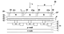
本発明の実施形態に係る撮像装置について説明する。図1Aは本実施形態の撮像装置の概略構成を示す断面図であり、図1Bは撮像装置に備えられている固体撮像素子の一部を示す模式断面図である。 An imaging apparatus according to an embodiment of the present invention will be described. FIG. 1A is a cross-sectional view illustrating a schematic configuration of the image pickup apparatus of the present embodiment, and FIG. 1B is a schematic cross-sectional view illustrating a part of a solid-state image pickup element provided in the image pickup apparatus.
図1Aに示すように、撮像装置100は、セラミックパッケージ101に組み込まれた固体撮像素子10と、開口絞り111を有するレンズホルダ102に、固体撮像素子10の素子表面(受光面)で結像するように配置固定されたレンズ112およびレンズ113とを備え、セラミックパッケージ101とレンズホルダ102とが一体化されてなる。なお、レンズ112およびレンズ113とからなるレンズ群115と固体撮像素子10との間には赤外光カットフィルタ105が備えられている。ここで、開口絞り111とレンズ群115とにより結像用光学系110が構成されている。
As shown in FIG. 1A, the
図1Bに示すように、固体撮像素子10は、半導体回路基板11と、半導体回路基板11上に二次元アレイ状に形成された複数の画素電極(下部電極)12と、複数の画素電極12上に連続し形成された有機材料からなる光電変換層14と、光電変換層14上に形成された、複数の画素電極に対向する対向電極であり、単一層として設けられた共通電極(上部電極)16とを備えている。また、上部電極16の上には透明な絶縁層18が積層されており、この絶縁層18上に、2色以上(本実施形態においては3色)のカラーフィルタ21r、21g、21bと各色のカラーフィルタ21r、21g、21bを隔てて分離する透明な分離壁22とからなるカラーフィルタ層CFが設けられ、さらにカラーフィルタ層CF上には低反射層25が設けられている。
As shown in FIG. 1B, the solid-
本撮像装置100は、開口絞り111を通過した光Lがレンズ112、レンズ113および赤外光カットフィルタ105を順次透過して固体撮像素子10の受光面に結像するよう構成されている。なお、ここで、レンズ113を透過し主光線の最大入射角αが45°以下となるように、レンズ群115および固体撮像素子10が配置構成されている。
The
また、画素ピッチD(μm)と固体撮像素子の受光面に入射する主光線の最大角度α(°)との関係が、
D≦2.6μmのとき、45≧α≧25・D−20
となるようにレンズ群115と固体撮像素子10との位置関係が設定されている。
Further, the relationship between the pixel pitch D (μm) and the maximum angle α (°) of the chief ray incident on the light receiving surface of the solid-state image sensor is
When D ≦ 2.6 μm, 45 ≧ α ≧ 25 · D-20
The positional relationship between the
画素ピッチD(μm)と主光線の最大角度α(°)との関係は、
D≦2.4μmのときには、45≧α≧25・D−15
となるようにレンズ群115と固体撮像素子10との位置関係を設定することが好ましい。
さらに、D≦2.0μmのときには、45≧α≧25・D−5
となるようにレンズ群115と固体撮像素子10との位置関係を設定することが好ましい。
The relationship between the pixel pitch D (μm) and the maximum chief ray angle α (°) is
When D ≦ 2.4 μm, 45 ≧ α ≧ 25 · D−15
It is preferable to set the positional relationship between the
Furthermore, when D ≦ 2.0 μm, 45 ≧ α ≧ 25 · D-5
It is preferable to set the positional relationship between the
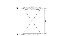
ここで単純な光学系にて本発明の効果を検証する。図2は1枚のレンズ201にて集光してイメージセンサ202上に等倍結像する場合を示している。画素ピッチを2.0μmとし、フルハイビジョン撮影をする場合、イメージセンサの大きさは、横2.0μm×1920=3.84mm、縦2.0μm×1080=2.16mm、となるため、対角としては4.4mmが必要となる。開口をイメージセンサと同じ4.4mmφを想定した場合、本発明の分離壁付きカラーフィルタ(図4A参照)を用いたイメージセンサであればNA=0.7のレンズを用いることでレンズとイメージセンサの距離dを4.4mmとすることが出来るのに対し、マイクロレンズ付きカラーフィルタ(図4B参照)ではNA=0.5のレンズまでしか許容できないことからレンズとイメージセンサの距離が7.6mmとなってしまう。実際の光学系は製品によって開口が異なることや、収差や周辺部の歪の影響を低減するために使用するレンズの枚数は1枚ではないし、複雑な非球面レンズを用いるために前記に示したような単純ではないが、効果としては原理的に同じで、光軸方向の長さを短くすることが可能となる。
Here, the effect of the present invention is verified with a simple optical system. FIG. 2 shows a case where the light is condensed by one
以下、各構成要素についての詳細を説明する。 Details of each component will be described below.
(半導体回路基板)
半導体回路基板11は、n型シリコン基板1(以下、単に基板1とする。)の表面にp型のウェル領域2を備え、ウェル領域2にはn型の不純物拡散領域3が複数形成されている。不純物拡散領域3は、回路基板11上に形成される画素電極12と対応して二次元アレイ状に形成されている。また、ウェル領域2の表面において、不純物拡散領域3の近傍には、該不純物拡散領域3に蓄積した電荷に応じた信号を出力する信号読出し部4が設けられている。
(Semiconductor circuit board)
The
信号読出し部4は、不純物拡散領域3に蓄積された電荷を電圧信号に変換して出力する回路であって、例えば公知のCCDやCMOS回路によって構成することができる。
The signal reading unit 4 is a circuit that converts the charge accumulated in the
さらに、基板1のウェル領域2が形成された表面上に絶縁層5が積層されている。絶縁層5の上には、平面視略矩形状の画素電極12が複数、所定の間隔で配列形成されている。各画素電極12は、絶縁層5を貫通するように形成された導電性材料からなる接続部6を介して、基板1の不純物拡散領域3に電気的に接続されている。
Further, an insulating layer 5 is laminated on the surface of the
撮像素子10は、光電変換層14に光が入射されると、光電変換層14で発生した電荷(正孔及び電子)のうち、例えば、正孔を上部電極16に移動させ、電子を下部電極12に移動させるように、下部電極12及び上部電極16間には、図示しない電圧供給部によってバイアス電圧が印加される。この場合、上部電極16を正孔捕集電極とし、下部電極12を電子捕集電極としている。
When light enters the
(電極)
上部電極16及び下部電極12は、光電変換層14との密着性や、電子親和力や、イオン化ポテンシャル、安定性等を考慮して選ばれる。
(electrode)
The
上部電極16及び下部電極12の作製には、その材料によって種々の方法が用いられるが、例えばITOの場合、電子ビーム法、スパッタリング法、抵抗加熱蒸着法、化学反応法(ゾルーゲル法など)、酸化インジウムスズの分散物の塗布などの方法で膜形成される。ITOの場合、UV−オゾン処理、プラズマ処理などを施すことができる。
Various methods are used to manufacture the
上部電極16は、光電変換層14に光を入射させる必要があるため、透明な導電性材料で構成されている。ここで、透明電極材料は、例えば波長が約420nm〜約660nmの範囲の可視光域で約80%以上の透過率であるものが好ましい。
The
上部電極16の具体的な材料としては、例えば、酸化スズ、酸化亜鉛、酸化インジウム、酸化インジウムスズ(ITO)等の導電性金属酸化物、あるいは金、銀、クロム、ニッケル等の金属、さらにこれらの金属と導電性金属酸化物との混合物または積層物、ヨウ化銅、硫化銅などの無機導電性物質、ポリアニリン、ポリチオフェン、ポリピロールなどの有機導電性材料、シリコン化合物およびこれらとITOとの積層物などが挙げられ、好ましくは、導電性の金属酸化物であり、特に、生産性、高導電性、透明性等の点からITO、ZnO、InO、が好ましい。
Specific examples of the material for the
下部電極12は、導電性材料であればよく、透明である必要はない。しかし、下部電極12の下方の基板1側にも光を透過させることが必要である場合には、下部電極12も透明電極材料で構成することが必要となる。このとき、下部電極12の透明電極材料としては、上部電極16と同様に、ITOを用いることが好ましい。
The
(光電変換層)
有機材料による光電変換層14は、厚みが0.1μmから1.0μmの範囲となるように成膜されている。光電変換層14の層厚は薄いほどイメージセンサの混色には有効となるが、光吸収とのトレードオフがあり、実質的には0.5μm程度が最適な層厚となる。
(Photoelectric conversion layer)
The
光電変換層14を構成する機材料としては、例えば電子写真の感光材料に用いられているような、様々な有機半導体材料を用いることができる。その中でも、高い光電変換性能を有すること、分光する際の色分離に優れていること、長時間の光照射に対する耐久性が高いこと、真空蒸着を行いやすいこと、等の観点から、キナクリドン骨格を含む材料やフタロシアニン骨格を含む有機材料が特に好ましい。
As a machine material constituting the
光電変換層14を構成する有機材料は、p型有機半導体及びn型有機半導体の少なくとも一方を含んでいることが好ましい。例えば、p型有機型半導体及びn型有機半導体として、それぞれキナクリドン誘導体、ナフタレン誘導体、アントラセン誘導体、フェナントレン誘導体、テトラセン誘導体、ピレン誘導体、ペリレン誘導体、及びフルオランテン誘導体のいずれかを特に好ましく用いることができる。
The organic material constituting the
光電変換層14を有機材料で構成すれば、シリコン基板などに形成したフォトダイオードを光電変換部として用いる構成に比べて、可視光に対する光吸収係数が大きい。このため、光電変換層14に入射した光が吸収されやすくなる。この性質によれば、光電変換層14に斜めに入射した光も隣接する画素部へ漏れにくくなり、画素部で光電変換されることになり、透過効率の向上とクロストークの抑制を図ることができる。
If the
(絶縁層)
絶縁層18は、Al2O3、SiO2、SiN、またはこれらの混合膜などから構成することができる。
(Insulating layer)
The insulating
(カラーフィルタ層)
図2に示すように、カラーフィルタ層CFは、それぞれ異なる波長の光を透過する複数のカラーフィルタを有する。ここでは、カラーフィルタCFは赤/青/緑色の顔料、もしくは染料の入った有機材料によるカラーフィルタ21r、21g、21bが画素毎に配置され、各カラーフィルタ21r、21g、21b間にはカラーフィルタ材料よりも屈折率が小さな透明材料で構成される分離壁22が設けられている。
(Color filter layer)
As shown in FIG. 2, the color filter layer CF includes a plurality of color filters that transmit light of different wavelengths. Here, the color filter CF includes
カラーフィルタ21r、21g、21bは、それぞれ異なる波長の光を透過するものであり、カラーフィルタ21rは、入射光のうち赤色の波長の光を透過する構成を有するR光カラーフィルタとして機能する。同様にカラーフィルタ21gは、入射光のうち緑色の波長の光を透過する構成を有するG光カラーフィルタとして、カラーフィルタ21bは、入射光のうち青色の波長の光を透過する構成を有するB光カラーフィルタとして機能する。
The
複数のカラーフィルタ21r,21g,21bは、各画素部にいずれか1つが含まれ、画素部の配列に応じてベイヤー配列などのカラーパターンで配列されている。図3では、一例として、4つの画素部におけるカラーフィルタ21r,21g,21bのベイヤー配列を示している。複数のカラーフィルタ21r,21g,21bの配列はこの構成例で説明するものに限定されず、任意に変更可能である。
Any one of the plurality of
カラーフィルタの屈折率は赤青緑の各色で異なり、また入射光の波長によっても異なるものであるが、カラーフィルタ21r、21g、21bのいずれも入射光波長(少なくともその可視光域の波長(400nm〜700nm)に対し1.5〜1.8の範囲内の屈折率を有する。
また、それぞれのカラーフィルタ21r、21g、21bの厚みは0.3μm〜1.0μmの範囲内としている。
The refractive index of the color filter is different for each color of red, blue, and green, and also varies depending on the wavelength of incident light. However, any of the
The thickness of each
カラーフィルタ21r,21g,21bを互いに分離するための分離壁22は、図3に示す平面視においては、略格子状に形成され、各カラーフィルタ21r,21g,21bそれぞれを個別に囲うように形成されている。
The
各カラーフィルタ21r、21g、21bの間隔に相当する分離壁22の幅tは0.05μm〜0.2μmの範囲内にあり、その屈折率は1.22〜1.34の範囲内にある。分離壁22の屈折率は低い程イメージセンサとしての特性は向上するが、あまり低い材料を用いると膜としての脆弱性が問題となることから実効的には1.28〜1.30程度の材料を用いることが望ましい。
The width t of the
(低反射層)
低反射層25は空気中からカラーフィルタCFに光がダイレクトに入射する場合の反射損失を低減するために備えられる。カラーフィルタCFに用いる材料の屈折率(例えば、3色のフィルタの屈折率の平均値)をncとした場合、低反射層25としては√ncとなる屈折率を有する材料を選択し、層厚は可視光のほぼ中心波長となる550nmの1/4膜厚となるようにすればよい。例えば、本素子の場合ではカラーフィルタCFの屈折率が1.5〜1.8であることから1.28前後の屈折率を有する材料を用い、厚さは550/4/1.28=107nmとなることから、約0.1μmとすればよい。
(Low reflective layer)
The
本実施形態の撮像装置は、以上のように構成されている。 The imaging device of the present embodiment is configured as described above.
本実施形態において撮像素子10は、基板1の上方に光電変換層14が積層された積層型撮像素子である。撮像素子は、従来の撮像素子のようなフォトダイオードが形成された基板上に電荷転送路が形成され、その上に平坦化膜などを挟んでカラーフィルタ層が設けられる表面照射型の撮像素子に比べ、カラーフィルタ層と光電変換層14との距離dを短くすることが可能である。具体的に、距離dは、カラーフィルタ層CFの下側面から光電変換層14の上側面までの距離である。本撮像素子の構成によれば、距離dを3μm以下とすることが可能である。
In the present embodiment, the
上記構成の撮像素子10を備えることにより、固体撮像素子10を備えた撮像装置100の厚さTを従来よりも小さくすることが可能となる。具体的には、固体撮像素子が1/4インチである場合に、従来装置であれば厚さTが通常5mm前後以上となるが、上記構成とすることにより4mmを下回る厚さを達成することができた。
By including the
(シミュレーション)
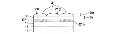
以下、本発明の撮像装置に備えられている分離壁22を有するカラーフィルタCFを備えた場合と、比較例として、分離壁を有さずマイクロレンズ31が備えられたカラーフィルタCF’を備えた場合とについて、光学シミュレーションを行った結果を説明する。
(simulation)
Hereinafter, when the color filter CF having the
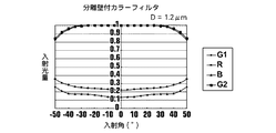
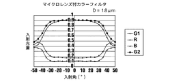
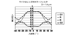
シミュレーションを行った素子構造の断面模式図を図4Aおよび図4Bに示す。図4Aが分離壁付きカラーフィルタを備えた場合の素子を示すものであり、図4Bがマイクロレンズ付きカラーフィルタを備えた場合の素子を示すものである。本シミュレーションにおいては、いずれも各色のカラーフィルタ21r、21g、21bを図3に示したようなベイヤー配列に配置したものとし、緑の画素領域における緑色フィルタを通って入射された光量と隣の画素(赤あるいは青)からの入射光量の入射角依存性を計算した。より詳細には、図3に示すカラーフィルタにおいて、G1−G1線上のR画素に隣接するG画素における入射光量をG1、およびこのG画素に隣接するR画素から入射する入射光量をRとし、入射角度をG1−G1線方向に変えていった場合の入射角度依存性を計算したものである。
同様にG2−G2線上のB画素に隣接するG画素における入射光量をG2、およびこのG画素に隣接するB画素から入射する入射光量をBとし、入射角度をG2−G2線方向に変えていった場合の入射角依存性を計算した。
4A and 4B are schematic cross-sectional views of the element structure in which the simulation was performed. FIG. 4A shows an element when a color filter with a separation wall is provided, and FIG. 4B shows an element when a color filter with a microlens is provided. In this simulation, it is assumed that the
Similarly, the incident light amount at the G pixel adjacent to the B pixel on the G2-G2 line is G2, and the incident light amount incident from the B pixel adjacent to the G pixel is B, and the incident angle is changed in the G2-G2 line direction. The incident angle dependence was calculated.
両構造とも光電変換層14としては有機材料を用いており厚さは0.5μmとし、カラーフィルタ層CFあるいはCF’との間には厚さ0.3μmの可視光に対し透明な絶縁層18を備えた構造とした。
In both structures, an organic material is used as the
分離壁付きカラーフィルタ層CFは分離壁22の幅を0.2μm、分離壁22の屈折率を1.3とした。本シミュレーションにおいて用いた各カラーフィルタ21r、21g、21bの膜厚は、0.7μm、0.5μm、0.5μmとした。
In the color filter layer CF with the separation wall, the width of the
マイクロレンズ付きカラーフィルタ層CF’の21r、21g、21bの膜厚は、0.7μm、0.5μm、0.5μmとした。カラーフィルタCF’とマイクロレンズ31との間に平坦化層30を備える構造とし、平坦化層の厚みは赤色カラーフィルタとマイクロレンズ31の間の厚さと定義した。また、マイクロレンズ31はレンズ厚tmが0.6μmとなる構造とした。
The film thicknesses of 21r, 21g, and 21b of the color filter layer CF ′ with a microlens were 0.7 μm, 0.5 μm, and 0.5 μm. The
平坦化層30の厚みは通常1〜2μmであるが、本シミュレーションでは平坦化層30の厚みを0μm、0.5μm、1.0μmと3種類の構造について計算した。平坦化層30はカラーフィルタ層CF’が現状の一般的な作製方法では表面に凹凸のある形状になってしまうこと、加えて各色毎にカラーフィルタの厚みが異なること等の理由から、マイクロレンズを安定に作製するために必要となる層である。現状一般的な厚みは1〜2μmと厚いものの、今後平坦化に用いる材料の技術進歩により将来は1μmよりも薄くして平坦化できる可能性がある。なお、マイクロレンズは平坦な面上に設ける必要があることから、現実的には平坦化層0μmはありえない値であり、せいぜい0.5μm程度が限界膜厚(最小膜厚)となると考えられる。
The thickness of the
シミュレーションにより得られた、混色が許容できる有効な入射角と画素ピッチの関係を示したものを図5に示す。なお、入射有効角は垂直入射時の光量よりも1割低減した時の入射角度と定義した。 FIG. 5 shows the relationship between the effective incident angle and the pixel pitch that can be mixed and obtained by simulation. The effective incidence angle was defined as the incidence angle when it was reduced by 10% from the amount of light at the time of vertical incidence.
図4Aに示した分離壁を有するカラーフィルタCFを備えた構造、および図4Bに示したマイクロレンズ付きカラーフィルタCF’を備えた構造であり、平坦化層1μm、0.5μm、0μmとした場合について、画素ピッチを1.8、1.4、1.2μmとした場合のそれぞれについてシミュレーションを行った。 When the structure includes the color filter CF having the separation wall illustrated in FIG. 4A and the structure including the color filter CF ′ with a microlens illustrated in FIG. 4B and the planarizing layer is 1 μm, 0.5 μm, and 0 μm A simulation was performed for each of the pixel pitches of 1.8, 1.4, and 1.2 μm.
図5に示す本シミュレーション結果によれば、従来のマイクロレンズ付きカラーフィルタ構造では、有機材料による薄い光電変換層であっても画素ピッチが小さくなるにつれて光入射角度が大きくなった際の混色が避けられず、最大有効入射角が小さくなることが分かった。これに対し分離壁付きカラーフィルタ構造、斜め入射による混色が劇的に小さくなり、最大有効入射角の許容範囲が大幅に増加することが分かった。 According to the simulation results shown in FIG. 5, in the conventional color filter structure with microlenses, even when the photoelectric conversion layer is made of an organic material, color mixture is avoided when the light incident angle increases as the pixel pitch decreases. It was found that the maximum effective incident angle was small. On the other hand, it was found that the color filter structure with a separation wall and the color mixture due to oblique incidence are drastically reduced, and the allowable range of the maximum effective incident angle is greatly increased.
図6〜図8は、図4Aに示す分離壁付きカラーフィルタを備えた場合であって、画素ピッチをそれぞれ1.8、1.4、1.2μmとした時のシミュレーション結果である。 6 to 8 show simulation results when the color filter with the separation wall shown in FIG. 4A is provided and the pixel pitch is 1.8, 1.4, and 1.2 μm, respectively.
図6〜図8に示すように、本発明の撮像装置では、画素ピッチDが1.8、1.4、1.2μmのいずれであっても45°まではほとんど劣化がないことが明らかとなった。 As shown in FIGS. 6 to 8, it is clear that the imaging apparatus of the present invention hardly deteriorates up to 45 ° regardless of the pixel pitch D of 1.8, 1.4, or 1.2 μm. became.
図9〜図11は、図4Bに示すマイクロレンズ付きカラーフィルタ(分離壁なし)を備え、平坦化層の厚みthを0.5μmとした場合であって、画素ピッチDをそれぞれ1.8、1.4、1.2μmとした時のシミュレーション結果である。 9 to 11, a color with a microlens filter (no separating wall), in a case where the thickness t h of the flattening layer was 0.5 [mu] m, the pixel pitch D respectively 1.8 shown in Figure 4B , 1.4, and 1.2 μm.
図9〜11に示すように、マイクロレンズ付きカラーフィルタ、平坦化層0.5μmを備えた素子においては、画素ピッチDが1.8μmの時(図9)、30°より大きな入射角になると入射光量及び混色特性が劣化し、同様に、画素ピッチDが1.4μmの時(図10)、20°より大きな入射角になると、画素ピッチDが1.2μmの時(図11)、15°より大きな入射角になるとそれぞれ顕著に入射光量及び混色特性が劣化していくのが分かる。 As shown in FIGS. 9 to 11, in an element provided with a color filter with a microlens and a flattening layer of 0.5 μm, when the pixel pitch D is 1.8 μm (FIG. 9), the incident angle is larger than 30 °. Similarly, when the incident light quantity and the color mixing characteristics deteriorate, and when the pixel pitch D is 1.4 μm (FIG. 10) and the incident angle is larger than 20 °, the pixel pitch D is 1.2 μm (FIG. 11), 15 It can be seen that the incident light quantity and the color mixing characteristics are significantly deteriorated when the incident angle is larger than °.
なお、図6〜図11において示すシミュレーション結果における縦軸(入射光量)は、図6に示すG1についての垂直入射(入射角0°)した際の光量を1として、規格化したものである。
Note that the vertical axis (incident light amount) in the simulation results shown in FIGS. 6 to 11 is normalized with the light amount when G1 shown in FIG. 6 is perpendicularly incident (
図5に示すように、マイクロレンズ付きカラーフィルタを備えた構造では、平坦化層の厚みが現実的な値である1.0μmの場合、画素ピッチDが1.8μmでは入射角が25°以上になると隣接画素からの混色が問題となる。同様に画素ピッチDが1.4μmでは15°、1.2μmでは10°より大きくなると混色による性能劣化が起き、画素ピッチに比例して画素ピッチが小さくなるほど有効な入射角が小さくなっている。すなわち、マイクロレンズ付きカラーフィルタを備えた構造では、平坦化層の厚み1.0μmの場合、図5の直線(1)より下の条件であれば良好な性能を得ることができる。
画素ピッチをD(μm)、有効入射角をα(°)とした場合、図5の直線(1)は、α=25・D−5であり、
α≧25・D−20の範囲でG光の入射光量の低下およびR光、B光の混色等の性能劣化が生じる。
As shown in FIG. 5, in the structure including the color filter with the microlens, the incident angle is 25 ° or more when the pixel pitch D is 1.8 μm when the thickness of the flattening layer is 1.0 μm which is a realistic value. Then, color mixing from adjacent pixels becomes a problem. Similarly, when the pixel pitch D is 1.4 [mu] m and 15 [deg.] And greater than 10 [deg.] When the pixel pitch D is greater than 10 [deg.], Performance deterioration due to color mixing occurs, and the effective incident angle decreases as the pixel pitch decreases in proportion to the pixel pitch. That is, in the structure including the color filter with microlenses, when the thickness of the planarization layer is 1.0 μm, good performance can be obtained under the condition below the straight line (1) in FIG.
When the pixel pitch is D (μm) and the effective incident angle is α (°), the straight line (1) in FIG. 5 is α = 25 · D-5,
In the range of α ≧ 25 · D−20, performance degradation such as a decrease in the amount of incident light of G light and color mixing of R light and B light occurs.
また、マイクロレンズ付きカラーフィルタを備えた構造で、平坦化層として用いる材料等に技術進歩により将来達成可能と考えられる平坦化層の最小膜厚である0.5μmの場合、図5の直線(2)より下の条件であれば良好な性能を得ることができる。
この場合、α≧25・D−15の範囲で性能劣化が生じる。
In the case of a structure provided with a color filter with a microlens and the minimum film thickness of the flattening layer considered to be achievable in the future due to technological advances in materials used as the flattening layer, the straight line in FIG. If the condition is lower than 2), good performance can be obtained.
In this case, performance degradation occurs in the range of α ≧ 25 · D-15.
さらに、マイクロレンズ付きカラーフィルタを備えた構造における製作上理論限界となる平坦化層0μmの場合で見ても、画素ピッチDが1.8μmでは入射角が40°以上になると隣接画素からの混色が問題となる。同様に画素ピッチDが1.4μmでは30°、1.2μmでは22.5°より大きくなると混色による性能劣化が起きている。
この場合、α≧25・D−5の範囲で性能劣化が生じることが明らかになった。
Further, even in the case of a flattening layer of 0 μm, which is a theoretical limit in manufacturing in a structure including a color filter with a microlens, when the incident angle becomes 40 ° or more when the pixel pitch D is 1.8 μm, color mixing from adjacent pixels is performed. Is a problem. Similarly, when the pixel pitch D is 1.4 [mu] m and 30 [deg.], And 1.2 [mu] m is greater than 22.5 [deg.], Performance deterioration due to color mixing occurs.
In this case, it became clear that performance degradation occurred in the range of α ≧ 25 · D-5.
これに対し、分離壁付きカラーフィルタではどの画素ピッチにおいても入射角に対する劣化が小さく、1.8μm、1.4μm、1.2μmのどの画素ピッチでも45°まで混色が問題とならないことがシミュレーションにより初めて明らかになった。従来のマイクロレンズ付きカラーフィルタでは画素ピッチが小さくなるほど最大入射角が小さくなっていることを考えると平坦化層の厚みにもよるが画素ピッチ2μm程度以上の範囲では混色が問題になることはなかったと考えられる。逆に画素ピッチが小さい範囲はシミュレーションでは1.2μmまでしか計算していないものの、画素ピッチが波長サイズ、つまり最長波長の赤色の波長である0.7μmをカラーフィルタの屈折率で割った約0.4μm程度までは有効であると考えられる。0.4μmよりも更に画素ピッチが小さい範囲では画素サイズが光の振幅よりも小さくなるために垂直入射でも混色が起きることが予想される。以上の考察より分離壁付きカラーフィルタが特に有効となる範囲は画素ピッチが0.4μm〜2μm程度の範囲であることが分かった。 On the other hand, in the color filter with a separation wall, the deterioration with respect to the incident angle is small at any pixel pitch, and the simulation shows that color mixing does not matter up to 45 ° at any pixel pitch of 1.8 μm, 1.4 μm, and 1.2 μm. First revealed. In consideration of the fact that the maximum incident angle becomes smaller as the pixel pitch becomes smaller in the conventional color filter with a microlens, color mixing does not become a problem in the range where the pixel pitch is about 2 μm or more, depending on the thickness of the planarization layer. It is thought. On the other hand, although the pixel pitch range is only calculated up to 1.2 μm in the simulation, the pixel pitch is the wavelength size, that is, the longest red wavelength of 0.7 μm divided by the refractive index of the color filter is about 0. Up to about 4 μm is considered effective. In a range where the pixel pitch is smaller than 0.4 μm, the pixel size is smaller than the amplitude of light, so that it is expected that color mixing occurs even at normal incidence. From the above considerations, it was found that the range in which the color filter with the separation wall is particularly effective is a range where the pixel pitch is about 0.4 μm to 2 μm.
以上のシミュレーション結果から、本発明においては、従来の構成では達成できなかった画素ピッチと入射有効角の範囲を規定した。すなわち、本発明は、最大入射角がマイクロレンズ付きカラーフィルタでは大きくロスが生じる入射角度以上であり、分離壁付きカラーフィルタを備えた素子において達成できる入射角度域を以下のように規定したものである。 From the above simulation results, in the present invention, the range of the pixel pitch and the effective incidence angle that could not be achieved by the conventional configuration was defined. That is, according to the present invention, the maximum incident angle is equal to or greater than the incident angle at which a large loss occurs in the color filter with a microlens, and the incident angle range that can be achieved in an element having a color filter with a separation wall is defined as follows. is there.
画素ピッチ2.6μm以下のとき、45≧α≧25・D−20、
さらに、画素ピッチ2.4μm以下のとき、45≧α≧25・D−15、
さらには、画素ピッチ2.0μm以下のとき、45≧α≧25・D−5とする。
When the pixel pitch is 2.6 μm or less, 45 ≧ α ≧ 25 · D-20,
Further, when the pixel pitch is 2.4 μm or less, 45 ≧ α ≧ 25 · D-15,
Further, when the pixel pitch is 2.0 μm or less, 45 ≧ α ≧ 25 · D−5.
なお、既述の通り、マイクロレンズ付きカラーフィルタの場合、平坦化層30を設けない構成すなわち平坦化層厚0μmは現実的ではない。平坦化層30を設けない構成とするためには、カラーフィルタ層において、各色のフィルタ厚みを同じにし、且つ各画素毎に平らになるようにして、隣の画素とのオーバラップも全くないようにパターニングする必要がある。しかし実際には各色毎に光吸収係数が異なるために、同じ厚さに揃えるのは技術的に困難であり、市販されている撮像装置に用いられているカラーフィルタは一般に各色毎のフィルタ厚さが異なっている。また表面を平らに加工するのは困難で、実際には端の部分が丸みを帯びた凸形状になっている。そのため赤青緑色のカラーフィルタを形成した表面は凸形状の各フィルタが敷き詰められた凸凹した表面形状になっている。マイクロレンズは平坦な面上に形成することを要することから、カラーフィルタの表面の凹凸を平坦化するための平坦化層30が必須となる。カラーフィルタ表面の凹凸の高低差はどんなに押さえ込んでも0.2〜0.3μm程度は残り、ここに樹脂を塗布して平坦にするためには少なくてもこの3倍程度の厚みを必要とする。従って現実的な平坦化層厚としては1μm程度が必要となるのである。
As described above, in the case of a color filter with a microlens, a configuration in which the
マイクロレンズ付きカラーフィルタを備えた構成では、画素ピッチが小さくなるにつれて、光入射有効角が小さくなる。したがって、光学系の全長を長くする必要があり、装置の小型化の弊害となっていた。
本発明で示した固体撮像素子は斜めから入射された光に対しても45°まではほとんど混色が問題にならない。したがって本撮像素子を用いた撮像装置は、αが45°以下となる光学系であれば任意の光学系と組み合わせて使用することが出来、従来のマイクロレンズを備えた素子において、各画素ピッチ毎に上限とされていた入射有効角よりも大きい角度の入射有効角を許容できるので、モジュールの全長を短くすることができ、小型化・薄型化に有効である。そのため例えばデジタルカメラや他の家電製品や携帯情報端末などに種々の用途で内蔵される撮像装置として効果的に利用することができる。
In the configuration including the color filter with a microlens, the effective light incident angle decreases as the pixel pitch decreases. Therefore, it is necessary to lengthen the entire length of the optical system, which has been an adverse effect of downsizing the apparatus.
In the solid-state imaging device shown in the present invention, color mixing hardly becomes a problem up to 45 ° with respect to light incident obliquely. Therefore, an image pickup apparatus using the present image pickup element can be used in combination with any optical system as long as α is 45 ° or less. In this case, the effective angle of incidence larger than the effective angle of incidence which is set as the upper limit can be allowed, so that the total length of the module can be shortened, which is effective for downsizing and thinning. Therefore, for example, it can be effectively used as an imaging device incorporated in various applications in a digital camera, other home appliances, a portable information terminal, and the like.
超広角で撮影を必要とする監視用カメラ、及び超薄型のデバイス形態が要求されるデジタルカメラ、ビデオカメラ、携帯電話等で利用可能である。 It can be used in surveillance cameras that require shooting at an ultra-wide angle, and digital cameras, video cameras, mobile phones, and the like that require ultra-thin device configurations.
10 固体撮像素子
11 半導体回路基板
12 下部電極(画素電極)
14 有機光電変換層
16 上部電極(共通電極)
18 絶縁層
21r、21g、21b カラーフィルタ
22 分離壁
30 平坦化層
31 マイクロレンズ
100 撮像装置
101 セラミックパッケージ
102 レンズホルダ
105 赤外光カットフィルタ
110 結像用光学系
111 開口絞り
112、113 レンズ
115 レンズ群
CF 分離壁付きカラーフィルタ
DESCRIPTION OF
14 Organic
18
Claims (3)
該結像用光学系の結像面に結像された画像を撮像する固体撮像素子とを備え、
該固体撮像素子が、基板上に複数の画素を有する撮像素子であって、有機材料からなる光電変換層、および該光電変換層の上方に配された2色以上のカラーフィルタと該各色のカラーフィルタを隔てて分離する透明な分離壁とからなるカラーフィルタ層を備え、
前記光電変換層の厚さが0.1μm〜1μmであり、
前記各色のカラーフィルタの屈折率がいずれも1.5〜1.8であり、
前記分離壁の幅が0.05μm〜0.2μmであり、
該分離壁の屈折率が1.22〜1.34であり、
前記固体撮像素子における画素ピッチD(μm)と該固体撮像素子に入射する主光線の最大角度α(°)との関係が、
D≦2.6μm
45≧α≧25・D−20
となるように前記レンズ群と前記固体撮像素子とが配置されていることを特徴とする撮像装置。 An imaging optical system including a lens group and an aperture stop;
A solid-state imaging device that images an image formed on the imaging surface of the imaging optical system,
The solid-state imaging device is an imaging device having a plurality of pixels on a substrate, a photoelectric conversion layer made of an organic material, two or more color filters disposed above the photoelectric conversion layer, and the color of each color A color filter layer comprising a transparent separation wall separating the filters,
The photoelectric conversion layer has a thickness of 0.1 μm to 1 μm,
The refractive index of each color filter is 1.5 to 1.8,
The width of the separation wall is 0.05 μm to 0.2 μm,
The separation wall has a refractive index of 1.22-1.34,
The relationship between the pixel pitch D (μm) in the solid-state image sensor and the maximum angle α (°) of the principal ray incident on the solid-state image sensor is
D ≦ 2.6 μm
45 ≧ α ≧ 25 · D-20
The imaging device, wherein the lens group and the solid-state imaging device are arranged so that
D≦2.4μm
45≧α≧25・D−15
であることを特徴とする請求項1記載の撮像装置。 The relationship between the pixel pitch D (μm) and the maximum angle α (°) of the principal ray is as follows:
D ≦ 2.4 μm
45 ≧ α ≧ 25 · D-15
The imaging apparatus according to claim 1, wherein:
D≦2.0μm
45≧α≧25・D−5
であることを特徴とする請求項1記載の撮像装置。 The relationship between the pixel pitch D (μm) and the maximum angle α (°) of the principal ray is as follows:
D ≦ 2.0μm
45 ≧ α ≧ 25 ・ D-5
The imaging apparatus according to claim 1, wherein:
Priority Applications (4)
| Application Number | Priority Date | Filing Date | Title |
|---|---|---|---|
| JP2011107759A JP2012238774A (en) | 2011-05-13 | 2011-05-13 | Image pickup device |
| PCT/JP2012/062721 WO2012157730A1 (en) | 2011-05-13 | 2012-05-11 | Imaging apparatus |
| KR1020137033140A KR101613346B1 (en) | 2011-05-13 | 2012-05-11 | Imaging apparatus |
| US14/076,827 US8988565B2 (en) | 2011-05-13 | 2013-11-11 | Imaging apparatus |
Applications Claiming Priority (1)
| Application Number | Priority Date | Filing Date | Title |
|---|---|---|---|
| JP2011107759A JP2012238774A (en) | 2011-05-13 | 2011-05-13 | Image pickup device |
Publications (2)
| Publication Number | Publication Date |
|---|---|
| JP2012238774A true JP2012238774A (en) | 2012-12-06 |
| JP2012238774A5 JP2012238774A5 (en) | 2014-03-06 |
Family
ID=47177046
Family Applications (1)
| Application Number | Title | Priority Date | Filing Date |
|---|---|---|---|
| JP2011107759A Abandoned JP2012238774A (en) | 2011-05-13 | 2011-05-13 | Image pickup device |
Country Status (4)
| Country | Link |
|---|---|
| US (1) | US8988565B2 (en) |
| JP (1) | JP2012238774A (en) |
| KR (1) | KR101613346B1 (en) |
| WO (1) | WO2012157730A1 (en) |
Cited By (9)
| Publication number | Priority date | Publication date | Assignee | Title |
|---|---|---|---|---|
| JP2014179577A (en) * | 2013-03-14 | 2014-09-25 | Visera Technologies Company Ltd | Solid-state imaging device |
| JP2015037155A (en) * | 2013-08-15 | 2015-02-23 | ソニー株式会社 | Image pickup element and image pickup device |
| US9478760B2 (en) | 2014-03-28 | 2016-10-25 | Panasonic Intellectual Property Management Co., Ltd. | Solid-state imaging device, imaging module, and imaging apparatus |
| US9559148B2 (en) | 2013-03-29 | 2017-01-31 | Fujifilm Corporation | Solid-state imaging device and imaging apparatus |
| JP2018056589A (en) * | 2017-12-12 | 2018-04-05 | ソニー株式会社 | Imaging element and imaging device |
| JP2018139272A (en) * | 2017-02-24 | 2018-09-06 | キヤノン株式会社 | Imaging element and imaging device |
| JP2020507201A (en) * | 2016-12-27 | 2020-03-05 | アレディア | Method of manufacturing optoelectronic device including photoluminescence pad of photoresist |
| KR20220086620A (en) | 2019-11-26 | 2022-06-23 | 후지필름 가부시키가이샤 | solid-state imaging device |
| JP2023152268A (en) * | 2022-03-31 | 2023-10-16 | 采▲ぎょく▼科技股▲ふん▼有限公司 | Image sensor and manufacturing method thereof |
Families Citing this family (9)
| Publication number | Priority date | Publication date | Assignee | Title |
|---|---|---|---|---|
| SG11201508691RA (en) | 2013-02-27 | 2015-11-27 | Univ North Carolina | Incoherent type-iii materials for charge carriers control devices |
| KR102328769B1 (en) | 2014-06-20 | 2021-11-18 | 삼성전자주식회사 | Image sensor and image processing system including the same |
| KR102299714B1 (en) | 2014-08-18 | 2021-09-08 | 삼성전자주식회사 | Image sensor including color filter isolation layer and method of fabricating the same |
| KR20160023158A (en) | 2014-08-21 | 2016-03-03 | 삼성전자주식회사 | Image sensor having improved light utilization efficiency and method of manufacturing the same |
| KR102282218B1 (en) | 2015-01-30 | 2021-07-26 | 삼성전자주식회사 | Imaging Optical System for 3D Image Acquisition Apparatus, and 3D Image Acquisition Apparatus Including the Imaging Optical system |
| US10203526B2 (en) * | 2015-07-06 | 2019-02-12 | The University Of North Carolina At Charlotte | Type III hetrojunction—broken gap HJ |
| US11675115B2 (en) * | 2018-10-19 | 2023-06-13 | Visera Technologies Company Limited | Optical devices |
| CN113359281B (en) * | 2018-12-05 | 2022-06-07 | 浙江舜宇光学有限公司 | Optical imaging lens group |
| US10955597B2 (en) * | 2019-01-04 | 2021-03-23 | Visera Technologies Company Limited | Optical devices |
Citations (6)
| Publication number | Priority date | Publication date | Assignee | Title |
|---|---|---|---|---|
| JP2009111225A (en) * | 2007-10-31 | 2009-05-21 | Fujifilm Corp | Solid-state image sensor and method of manufacturing the same |
| JP2010067827A (en) * | 2008-09-11 | 2010-03-25 | Fujifilm Corp | Solid-state imaging device and imaging apparatus |
| JP2010074218A (en) * | 2008-09-16 | 2010-04-02 | Dainippon Printing Co Ltd | Solid-state image pickup element and method of manufacturing the same, and image pickup apparatus using the solid-state image pickup element |
| JP2010212455A (en) * | 2009-03-10 | 2010-09-24 | Nippon Hoso Kyokai <Nhk> | Organic photoelectric conversion film and electronic element including the same |
| JP2010232537A (en) * | 2009-03-27 | 2010-10-14 | Fujifilm Corp | Imaging element |
| JP2010272654A (en) * | 2009-05-20 | 2010-12-02 | Panasonic Corp | Solid-state image pickup device and manufacturing method thereof |
Family Cites Families (4)
| Publication number | Priority date | Publication date | Assignee | Title |
|---|---|---|---|---|
| JP4828317B2 (en) | 2005-09-29 | 2011-11-30 | 富士フイルム株式会社 | Imaging lens |
| JP4910723B2 (en) | 2007-01-29 | 2012-04-04 | コニカミノルタオプト株式会社 | Imaging lens, imaging device, and portable terminal |
| KR100940235B1 (en) | 2007-04-24 | 2010-02-04 | 삼성테크윈 주식회사 | Photographic lens |
| JP5478043B2 (en) | 2008-09-11 | 2014-04-23 | 富士フイルム株式会社 | Solid-state imaging device and imaging apparatus |
-
2011
- 2011-05-13 JP JP2011107759A patent/JP2012238774A/en not_active Abandoned
-
2012
- 2012-05-11 KR KR1020137033140A patent/KR101613346B1/en active IP Right Grant
- 2012-05-11 WO PCT/JP2012/062721 patent/WO2012157730A1/en active Application Filing
-
2013
- 2013-11-11 US US14/076,827 patent/US8988565B2/en active Active
Patent Citations (6)
| Publication number | Priority date | Publication date | Assignee | Title |
|---|---|---|---|---|
| JP2009111225A (en) * | 2007-10-31 | 2009-05-21 | Fujifilm Corp | Solid-state image sensor and method of manufacturing the same |
| JP2010067827A (en) * | 2008-09-11 | 2010-03-25 | Fujifilm Corp | Solid-state imaging device and imaging apparatus |
| JP2010074218A (en) * | 2008-09-16 | 2010-04-02 | Dainippon Printing Co Ltd | Solid-state image pickup element and method of manufacturing the same, and image pickup apparatus using the solid-state image pickup element |
| JP2010212455A (en) * | 2009-03-10 | 2010-09-24 | Nippon Hoso Kyokai <Nhk> | Organic photoelectric conversion film and electronic element including the same |
| JP2010232537A (en) * | 2009-03-27 | 2010-10-14 | Fujifilm Corp | Imaging element |
| JP2010272654A (en) * | 2009-05-20 | 2010-12-02 | Panasonic Corp | Solid-state image pickup device and manufacturing method thereof |
Cited By (12)
| Publication number | Priority date | Publication date | Assignee | Title |
|---|---|---|---|---|
| JP2014179577A (en) * | 2013-03-14 | 2014-09-25 | Visera Technologies Company Ltd | Solid-state imaging device |
| US9502453B2 (en) | 2013-03-14 | 2016-11-22 | Visera Technologies Company Limited | Solid-state imaging devices |
| US9559148B2 (en) | 2013-03-29 | 2017-01-31 | Fujifilm Corporation | Solid-state imaging device and imaging apparatus |
| JP2015037155A (en) * | 2013-08-15 | 2015-02-23 | ソニー株式会社 | Image pickup element and image pickup device |
| US9478760B2 (en) | 2014-03-28 | 2016-10-25 | Panasonic Intellectual Property Management Co., Ltd. | Solid-state imaging device, imaging module, and imaging apparatus |
| JP2020507201A (en) * | 2016-12-27 | 2020-03-05 | アレディア | Method of manufacturing optoelectronic device including photoluminescence pad of photoresist |
| JP7360325B2 (en) | 2016-12-27 | 2023-10-12 | アレディア | Method for manufacturing optoelectronic devices |
| JP2018139272A (en) * | 2017-02-24 | 2018-09-06 | キヤノン株式会社 | Imaging element and imaging device |
| JP7071055B2 (en) | 2017-02-24 | 2022-05-18 | キヤノン株式会社 | Image sensor and image sensor |
| JP2018056589A (en) * | 2017-12-12 | 2018-04-05 | ソニー株式会社 | Imaging element and imaging device |
| KR20220086620A (en) | 2019-11-26 | 2022-06-23 | 후지필름 가부시키가이샤 | solid-state imaging device |
| JP2023152268A (en) * | 2022-03-31 | 2023-10-16 | 采▲ぎょく▼科技股▲ふん▼有限公司 | Image sensor and manufacturing method thereof |
Also Published As
| Publication number | Publication date |
|---|---|
| US8988565B2 (en) | 2015-03-24 |
| WO2012157730A1 (en) | 2012-11-22 |
| KR20140041548A (en) | 2014-04-04 |
| KR101613346B1 (en) | 2016-04-18 |
| US20140071316A1 (en) | 2014-03-13 |
Similar Documents
| Publication | Publication Date | Title |
|---|---|---|
| JP2012238774A (en) | Image pickup device | |
| JP4741015B2 (en) | Image sensor | |
| JP5556122B2 (en) | Solid-state imaging device, manufacturing method of solid-state imaging device, and electronic apparatus | |
| US9131100B2 (en) | Solid-state imaging device with lens, method of manufacturing solid-state imaging device with lens, and electronic apparatus | |
| JP4538353B2 (en) | Photoelectric conversion film stacked color solid-state imaging device | |
| US10043840B2 (en) | Image sensor and electronic device including the same | |
| WO2011142065A1 (en) | Solid-state image pickup device and method for manufacturing same | |
| JP2011258728A (en) | Solid state image sensor and electronic information apparatus | |
| JP5032954B2 (en) | Color imaging device | |
| WO2013114824A1 (en) | Imaging element | |
| JP5866248B2 (en) | Solid-state image sensor | |
| JP2004047682A (en) | Solid-state image pickup device | |
| JP5504382B2 (en) | Solid-state imaging device and imaging apparatus | |
| JP2013207053A (en) | Solid state imaging device and electronic apparatus | |
| JP2016152265A (en) | Solid-state image pickup device | |
| JP2014022649A (en) | Solid-state image sensor, imaging device, and electronic apparatus | |
| JP2013076859A (en) | Manufacturing method for color filter, manufacturing method for solid state imager, and solid state imager | |
| JP2012234968A (en) | Solid state image pickup device, manufacturing method of the same and electronic information apparatus | |
| US8138467B2 (en) | Color filter array including color filters only of first type and second type, method of fabricating the same, and image pickup device including the same | |
| WO2013031160A1 (en) | Solid state image capture device and method of manufacturing same | |
| JP2012099743A (en) | Solid-state imaging device and manufacturing method therefor | |
| JP2012151421A (en) | Image sensing device | |
| JP7474943B2 (en) | Imaging device | |
| CN117855234A (en) | Image sensor | |
| JP2023037557A (en) | Solid state image sensor |
Legal Events
| Date | Code | Title | Description |
|---|---|---|---|
| A521 | Request for written amendment filed |
Free format text: JAPANESE INTERMEDIATE CODE: A523 Effective date: 20140120 |
|
| A621 | Written request for application examination |
Free format text: JAPANESE INTERMEDIATE CODE: A621 Effective date: 20140120 |
|
| A131 | Notification of reasons for refusal |
Free format text: JAPANESE INTERMEDIATE CODE: A131 Effective date: 20140603 |
|
| A762 | Written abandonment of application |
Free format text: JAPANESE INTERMEDIATE CODE: A762 Effective date: 20140714 |