JP2020113573A - Photoelectric conversion device - Google Patents
Photoelectric conversion device Download PDFInfo
- Publication number
- JP2020113573A JP2020113573A JP2019001145A JP2019001145A JP2020113573A JP 2020113573 A JP2020113573 A JP 2020113573A JP 2019001145 A JP2019001145 A JP 2019001145A JP 2019001145 A JP2019001145 A JP 2019001145A JP 2020113573 A JP2020113573 A JP 2020113573A
- Authority
- JP
- Japan
- Prior art keywords
- photoelectric conversion
- conversion device
- pixel
- conversion unit
- region
- Prior art date
- Legal status (The legal status is an assumption and is not a legal conclusion. Google has not performed a legal analysis and makes no representation as to the accuracy of the status listed.)
- Pending
Links
- 238000006243 chemical reaction Methods 0.000 title claims abstract description 150
- 238000012546 transfer Methods 0.000 claims abstract description 80
- 238000003384 imaging method Methods 0.000 claims abstract description 70
- 238000009792 diffusion process Methods 0.000 claims abstract description 40
- 239000011159 matrix material Substances 0.000 claims abstract description 5
- 239000012535 impurity Substances 0.000 claims description 23
- 238000012545 processing Methods 0.000 claims description 19
- 239000004065 semiconductor Substances 0.000 claims description 12
- 238000000034 method Methods 0.000 claims description 3
- 238000000926 separation method Methods 0.000 claims description 2
- 239000000203 mixture Substances 0.000 abstract description 11
- 230000002093 peripheral effect Effects 0.000 description 17
- 238000010586 diagram Methods 0.000 description 12
- 230000003287 optical effect Effects 0.000 description 11
- 229920006395 saturated elastomer Polymers 0.000 description 10
- 238000001514 detection method Methods 0.000 description 6
- 238000005036 potential barrier Methods 0.000 description 3
- 102000004129 N-Type Calcium Channels Human genes 0.000 description 2
- 108090000699 N-Type Calcium Channels Proteins 0.000 description 2
- 230000000694 effects Effects 0.000 description 2
- 238000002955 isolation Methods 0.000 description 2
- 230000003321 amplification Effects 0.000 description 1
- 238000004364 calculation method Methods 0.000 description 1
- 239000003086 colorant Substances 0.000 description 1
- 238000004891 communication Methods 0.000 description 1
- 238000004590 computer program Methods 0.000 description 1
- 238000012790 confirmation Methods 0.000 description 1
- 230000007547 defect Effects 0.000 description 1
- 230000002950 deficient Effects 0.000 description 1
- 230000031700 light absorption Effects 0.000 description 1
- 239000004973 liquid crystal related substance Substances 0.000 description 1
- 238000005259 measurement Methods 0.000 description 1
- 238000003199 nucleic acid amplification method Methods 0.000 description 1
- 238000005192 partition Methods 0.000 description 1
- 239000000758 substrate Substances 0.000 description 1
Images


Classifications
-
- H—ELECTRICITY
- H01—ELECTRIC ELEMENTS
- H01L—SEMICONDUCTOR DEVICES NOT COVERED BY CLASS H10
- H01L27/00—Devices consisting of a plurality of semiconductor or other solid-state components formed in or on a common substrate
- H01L27/14—Devices consisting of a plurality of semiconductor or other solid-state components formed in or on a common substrate including semiconductor components sensitive to infrared radiation, light, electromagnetic radiation of shorter wavelength or corpuscular radiation and specially adapted either for the conversion of the energy of such radiation into electrical energy or for the control of electrical energy by such radiation
- H01L27/144—Devices controlled by radiation
- H01L27/146—Imager structures
- H01L27/14601—Structural or functional details thereof
- H01L27/14625—Optical elements or arrangements associated with the device
- H01L27/14627—Microlenses
-
- G—PHYSICS
- G05—CONTROLLING; REGULATING
- G05D—SYSTEMS FOR CONTROLLING OR REGULATING NON-ELECTRIC VARIABLES
- G05D1/00—Control of position, course or altitude of land, water, air, or space vehicles, e.g. automatic pilot
- G05D1/02—Control of position or course in two dimensions
- G05D1/021—Control of position or course in two dimensions specially adapted to land vehicles
- G05D1/0231—Control of position or course in two dimensions specially adapted to land vehicles using optical position detecting means
- G05D1/0246—Control of position or course in two dimensions specially adapted to land vehicles using optical position detecting means using a video camera in combination with image processing means
-
- H—ELECTRICITY
- H01—ELECTRIC ELEMENTS
- H01L—SEMICONDUCTOR DEVICES NOT COVERED BY CLASS H10
- H01L27/00—Devices consisting of a plurality of semiconductor or other solid-state components formed in or on a common substrate
- H01L27/14—Devices consisting of a plurality of semiconductor or other solid-state components formed in or on a common substrate including semiconductor components sensitive to infrared radiation, light, electromagnetic radiation of shorter wavelength or corpuscular radiation and specially adapted either for the conversion of the energy of such radiation into electrical energy or for the control of electrical energy by such radiation
- H01L27/144—Devices controlled by radiation
- H01L27/146—Imager structures
- H01L27/14601—Structural or functional details thereof
- H01L27/14603—Special geometry or disposition of pixel-elements, address-lines or gate-electrodes
- H01L27/14605—Structural or functional details relating to the position of the pixel elements, e.g. smaller pixel elements in the center of the imager compared to pixel elements at the periphery
-
- H—ELECTRICITY
- H01—ELECTRIC ELEMENTS
- H01L—SEMICONDUCTOR DEVICES NOT COVERED BY CLASS H10
- H01L27/00—Devices consisting of a plurality of semiconductor or other solid-state components formed in or on a common substrate
- H01L27/14—Devices consisting of a plurality of semiconductor or other solid-state components formed in or on a common substrate including semiconductor components sensitive to infrared radiation, light, electromagnetic radiation of shorter wavelength or corpuscular radiation and specially adapted either for the conversion of the energy of such radiation into electrical energy or for the control of electrical energy by such radiation
- H01L27/144—Devices controlled by radiation
- H01L27/146—Imager structures
- H01L27/14601—Structural or functional details thereof
- H01L27/14609—Pixel-elements with integrated switching, control, storage or amplification elements
- H01L27/14612—Pixel-elements with integrated switching, control, storage or amplification elements involving a transistor
-
- H—ELECTRICITY
- H01—ELECTRIC ELEMENTS
- H01L—SEMICONDUCTOR DEVICES NOT COVERED BY CLASS H10
- H01L27/00—Devices consisting of a plurality of semiconductor or other solid-state components formed in or on a common substrate
- H01L27/14—Devices consisting of a plurality of semiconductor or other solid-state components formed in or on a common substrate including semiconductor components sensitive to infrared radiation, light, electromagnetic radiation of shorter wavelength or corpuscular radiation and specially adapted either for the conversion of the energy of such radiation into electrical energy or for the control of electrical energy by such radiation
- H01L27/144—Devices controlled by radiation
- H01L27/146—Imager structures
- H01L27/14601—Structural or functional details thereof
- H01L27/1463—Pixel isolation structures
-
- H—ELECTRICITY
- H01—ELECTRIC ELEMENTS
- H01L—SEMICONDUCTOR DEVICES NOT COVERED BY CLASS H10
- H01L27/00—Devices consisting of a plurality of semiconductor or other solid-state components formed in or on a common substrate
- H01L27/14—Devices consisting of a plurality of semiconductor or other solid-state components formed in or on a common substrate including semiconductor components sensitive to infrared radiation, light, electromagnetic radiation of shorter wavelength or corpuscular radiation and specially adapted either for the conversion of the energy of such radiation into electrical energy or for the control of electrical energy by such radiation
- H01L27/144—Devices controlled by radiation
- H01L27/146—Imager structures
- H01L27/14601—Structural or functional details thereof
- H01L27/14636—Interconnect structures
-
- H—ELECTRICITY
- H04—ELECTRIC COMMUNICATION TECHNIQUE
- H04N—PICTORIAL COMMUNICATION, e.g. TELEVISION
- H04N25/00—Circuitry of solid-state image sensors [SSIS]; Control thereof
- H04N25/70—SSIS architectures; Circuits associated therewith
- H04N25/702—SSIS architectures characterised by non-identical, non-equidistant or non-planar pixel layout
-
- H—ELECTRICITY
- H04—ELECTRIC COMMUNICATION TECHNIQUE
- H04N—PICTORIAL COMMUNICATION, e.g. TELEVISION
- H04N25/00—Circuitry of solid-state image sensors [SSIS]; Control thereof
- H04N25/70—SSIS architectures; Circuits associated therewith
- H04N25/76—Addressed sensors, e.g. MOS or CMOS sensors
- H04N25/77—Pixel circuitry, e.g. memories, A/D converters, pixel amplifiers, shared circuits or shared components
-
- H—ELECTRICITY
- H01—ELECTRIC ELEMENTS
- H01L—SEMICONDUCTOR DEVICES NOT COVERED BY CLASS H10
- H01L27/00—Devices consisting of a plurality of semiconductor or other solid-state components formed in or on a common substrate
- H01L27/14—Devices consisting of a plurality of semiconductor or other solid-state components formed in or on a common substrate including semiconductor components sensitive to infrared radiation, light, electromagnetic radiation of shorter wavelength or corpuscular radiation and specially adapted either for the conversion of the energy of such radiation into electrical energy or for the control of electrical energy by such radiation
- H01L27/144—Devices controlled by radiation
- H01L27/146—Imager structures
- H01L27/14601—Structural or functional details thereof
- H01L27/14641—Electronic components shared by two or more pixel-elements, e.g. one amplifier shared by two pixel elements
Abstract
Description
本発明は、光電変換装置に関する。 The present invention relates to a photoelectric conversion device.
近年さまざまな分野で用いられているデジタルカメラは少なくとも撮像レンズと固体撮像装置(光電変換装置)から構成されている。固体撮像装置は撮像領域面内に画素が行列状に配置されているが、撮像領域中央部では入射光の主光線が垂直に入るのに対し、周辺部では入射光の主光線が斜めになるため周辺部画素の出力が下がるシェーディングや隣接画素への混色を引き起こす。 Digital cameras used in various fields in recent years include at least an imaging lens and a solid-state imaging device (photoelectric conversion device). In the solid-state image pickup device, pixels are arranged in a matrix in the image pickup area plane, but the chief ray of the incident light enters vertically in the central part of the image pickup area, whereas the chief ray of the incident light becomes oblique in the peripheral part Therefore, the shading that the output of the peripheral pixel is lowered and the color mixture to the adjacent pixel are caused.
そのため一般的にはマイクロレンズを撮像領域中心側にシフトさせたり、逆に光電変換部を画面周辺側にシフトさせたりして、光が効率よく光電変換部に受光されるような構造が提案されている(特許文献1)。 Therefore, generally, a structure is proposed in which the microlens is shifted to the center side of the imaging area, or conversely, the photoelectric conversion section is shifted to the peripheral side of the screen so that the light is efficiently received by the photoelectric conversion section. (Patent Document 1).
しかしながら光電変換部を画素領域(撮像領域)の周辺側にシフトさせた場合、光電変換部と転送ゲート及びフローティングディフュージョン間の相対的な位置関係が画素領域面内の画素毎に変わってしまう。この影響により、一部の画素で転送不良や飽和電荷量不足などの問題が発生してしまう。 However, when the photoelectric conversion unit is shifted to the peripheral side of the pixel region (imaging region), the relative positional relationship between the photoelectric conversion unit, the transfer gate, and the floating diffusion changes for each pixel in the pixel region surface. Due to this influence, problems such as defective transfer and insufficient saturated charge amount occur in some pixels.
また光電変換部のシフトに合わせて転送ゲート及びフローティングディフュージョンもシフトさせると、それらに接続されるコンタクトホールや配線のパターンも変わって画素レイアウト上の制約が大きくなり、画素性能を最大化することが難しくなる。 Further, when the transfer gate and the floating diffusion are also shifted in accordance with the shift of the photoelectric conversion unit, the contact hole and wiring pattern connected to them are also changed, and the constraint on the pixel layout is increased, so that the pixel performance can be maximized. It gets harder.
本発明では、光電変換部からフローティングディフュージョンへの転送特性や飽和電荷量を面内均一に保ちつつ、光電変換部シフトによるシェーディング改善、混色低減された光電変換装置を提供することを目的とする。 An object of the present invention is to provide a photoelectric conversion device in which shading is improved and color mixing is reduced by shifting the photoelectric conversion unit while keeping the transfer characteristics from the photoelectric conversion unit to the floating diffusion and the amount of saturated charges in-plane uniform.
本発明の一態様は、光電変換部と、フローティングディフュージョンと、前記光電変換部で発生した電荷の前記フローティングディフュージョンへの転送を制御する転送ゲートとを有する画素が、マトリクス状に配列された画素領域を備える光電変換装置であって、前記画素領域内の位置に応じて前記光電変換部が前記転送ゲートに対して相対的にシフトしており、前記シフトの方向は前記光電変換部から前記フローティングディフュージョンへの電荷転送方向に直交する方向であることを特徴とする。 One embodiment of the present invention is a pixel region in which pixels each having a photoelectric conversion portion, a floating diffusion, and a transfer gate which controls transfer of charges generated in the photoelectric conversion portion to the floating diffusion are arranged in matrix. In the photoelectric conversion device, the photoelectric conversion unit is relatively shifted with respect to the transfer gate according to a position in the pixel region, and a direction of the shift is from the photoelectric conversion unit to the floating diffusion. It is characterized in that the direction is orthogonal to the direction of charge transfer to.
本発明によって、画素領域面内の転送特性や飽和電荷量を均一に保ちながら、光電変換部シフトによるシェーディング改善、混色低減された光電変換装置を提供することが可能になる。 According to the present invention, it is possible to provide a photoelectric conversion device in which the shading is improved and the color mixture is reduced by shifting the photoelectric conversion unit while keeping the transfer characteristics and the saturated charge amount in the pixel area plane uniform.
本発明の光電変換装置(固体撮像装置)の構成について、複数の実施形態を用いて説明を行う。各実施形態は本発明の一部であり適宜変更可能であるためこれに限定されるものではない。また複数の実施形態を組み合わせることも可能である。また、以下の実施形態では、第1導電型がP型であり、第2導電型がN型である。しかしながら、第1導電型と第2導電型は極性が反対であれば、第1導電型がN型であり、第2導電型がP型であってもよい。 The configuration of the photoelectric conversion device (solid-state imaging device) of the present invention will be described using a plurality of embodiments. Each embodiment is part of the present invention and can be modified as appropriate, and thus is not limited to this. It is also possible to combine a plurality of embodiments. In the following embodiments, the first conductivity type is P type and the second conductivity type is N type. However, if the first conductivity type and the second conductivity type have opposite polarities, the first conductivity type may be the N type and the second conductivity type may be the P type.
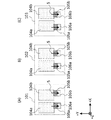
(実施形態1)
図1は、本実施形態にかかる固体撮像装置において複数の画素がマトリクス状に配列された画素領域(撮像領域)1を示す平面図である。画素領域1を構成する画素は実際には数百万から数千万個存在するが、ここでは説明の便宜上画素数を減らして簡略化している。画素領域1の中央部にある画素を画素12、周辺部左側の画素を画素11、周辺部右側の画素を画素13と称する。
(Embodiment 1)
FIG. 1 is a plan view showing a pixel region (imaging region) 1 in which a plurality of pixels are arranged in a matrix in the solid-state imaging device according to the present embodiment. Actually, there are millions to tens of millions of pixels forming the
図2A〜図2Cは各画素構造を説明するための平面図であり、図2Aは画素11を、図2Bは画素12を、図2Cは画素13をそれぞれ説明する図である。いずれの画素も、光電変換部2と、転送ゲート3と、フローティングディフュージョン4を含む。転送ゲート3は転送トランジスタのゲートである。また、光電変換部2は転送トランジスタのソースであり、フローティングディフュージョン4は転送トランジスタのドレインである。本実施形態ではPウエル中(第1半導体領域中)に形成されたN型不純物領域(第2半導体領域)が光電変換部2に相当する。つまり図2の光電変換部2がN型不純物領域と等しい。
2A to 2C are plan views for explaining each pixel structure, FIG. 2A is a diagram illustrating the
光電変換部2は光を光電変換して電荷を発生、蓄積させる機能を有する。転送ゲート3は光電変換部2で蓄積された電荷を転送ゲート3直下に形成されるN型チャネルを経由させてフローティングディフュージョン4へ転送させる機能を有する。本実施形態では、転送ゲート3からフローティングディフュージョン4への電荷転送方向は全ての画素において同一方向(−Y方向)である。フローティングディフュージョン4は光電変換部2から転送された電荷を電気信号として読み出せるように電圧に変換する機能を有する。
The
画素11、画素12、画素13を比較すると、転送ゲート3に対する光電変換部2の位置が異なっている。具体的には、各画素内の光電変換部2は、画素領域内での画素位置に応じた量だけ、転送ゲート3に対して相対的にシフトしている。シフト方向は電荷転送方向5に直交するX軸方向と平行な方向であり、より具体的には、画素領域周辺側に向かう方向である。例えば画素11においては画素12と比較して転送ゲート3に対する光電変換部2の相対位置が−X方向へシフトしている。また画素13においては画素12と比較して転送ゲート3に対する光電変換部2の相対位置が+X方向へシフトしている。この時
転送ゲート3やフローティングディフュージョン4はシフトしない。また、光電変換部2はY方向にはシフトしない。すなわち、光電変換部2と転送ゲート3およびフローティングディフュージョン4のY方向についての相対位置関係は全ての画素で同じである。
Comparing the
本実施形態において、各画素中における転送ゲート3およびフローティングディフュージョン4の位置は同じである。そして、画素内における光電変換部2のY方向の位置は、全ての画素において同じであるが、光電変換部2のX方向の位置が画素に応じて異なっている。
In this embodiment, the positions of the transfer gate 3 and the floating diffusion 4 in each pixel are the same. The position of the
なお、転送ゲート3およびフローティングディフュージョン4の画素内での配置は画素ごとに異なっていてもよい。この場合も、上述したように、光電変換部2の転送ゲート3およびフローティングディフュージョン4に対する相対位置のうち、X方向の位置が画素に応じて異なっており、Y方向の位置は全ての画素について同じである。
The arrangement of the transfer gate 3 and the floating diffusion 4 in the pixel may be different for each pixel. Also in this case, as described above, of the relative positions of the
図3は本実施形態における画素領域内の光電変換部2のシフト方向及びシフト量を模式的に示した図であり、図4は光電変換部2のシフト量の大きさをより詳細に示した図になる。光電変換部2のシフト量の大きさは画素領域中心からのX方向距離(絶対値)によって決まるため、図3の光電変換部2のシフト31が示すように行方向では周辺画素ほど光電変換部2のシフト量が大きい。一方、同じ列に配置される画素における光電変換部2のシフト31の量は同一である。本実施形態では図4の直線41に示すように画素領域中央列からのX方向距離に比例して線形的にシフト量を大きくさせている。しかし、X方向距離とシフト量の関係は線形な変化に限定されず、広義単調増加な変化であればよい。すなわち、シフト量は画素領域1の中央列からの距離が離れた画素ほど大きければよく、例えば、直線42のようにあるX方向距離から線形的にシフト量を大きくしても良いし、曲線43のように非線形的にシフト量を変化させても良い。
FIG. 3 is a diagram schematically showing the shift direction and the shift amount of the
また図2には図示していないが、それぞれの画素は転送ゲート3の他にもリセットトランジスタ、増幅トランジスタ、行選択トランジスタを含む。これらのトランジスタは通常、隣接する画素の境界部に配置されるが、光電変換部2のシフト可能範囲を広げられるように、X方向のN型不純物領域間を避けて配置されことが望ましい。換言すると、X方向に隣接する画素の光電変換部2の間の領域には、トランジスタが配置されないことが望ましい。
Although not shown in FIG. 2, each pixel includes a reset transistor, an amplification transistor, and a row selection transistor in addition to the transfer gate 3. These transistors are usually arranged at the boundary between adjacent pixels, but it is preferable to arrange them so as to avoid the N-type impurity regions in the X direction so that the shiftable range of the
図5A〜図5Cは図2で示した画素11〜13の画素中心A−A′、B−B′、C−C′におけるX方向断面図である。それぞれの画素は、光電変換部2が形成される半導体基板6と、光電変換部上に配置される配線層7・カラーフィルタ8・マイクロレンズ9から構成されている。配線層7には光が光電変換部2に入射できるように開口部が設けられる。カラーフィルタ8は色を分離する。マイクロレンズ9は入射光の集光機能を有する。
5A to 5C are cross-sectional views in the X direction at pixel centers AA', BB', and CC' of the
画素領域中央の画素12には垂直方向(−Z方向)に光が入射するが、画素領域周辺の画素11や画素13では画素領域中央から周辺へ向かって斜めに光が入射する。そのため配線層7に光が当たらないようにマイクロレンズ9は画素領域中央側へシフトさせている。マイクロレンズ9のシフト方向は画素領域中心方向に放射状になっており、画素領域中心からの距離に比例してマイクロレンズ9のシフト量は大きくなる。
Light enters the
しかし図5A、図5Cのように配線層7による光の反射及び吸収を最小化させるべくマイクロレンズ9をシフトした場合、入射光が光電変換部2表面に作るスポット(集光位置)は画素中心よりも画素領域周辺側にシフトする。そこで本実施形態では画素11及び画素13の光電変換部2をそれぞれ画素領域周辺方向へシフトさせている。
However, when the
このように光電変換部2をシフトすることで画素領域周辺部において、入射光10を効率的に光電変換部2で受光できるようになる。したがって、周辺部での輝度低下(輝度シェーディング)や隣接画素への混色を抑制することが可能となり画質を向上させることが可能になる。
By shifting the
本実施形態において光電変換部2がシフトするのはX方向だけであり、光電変換部2からフローティングディフュージョン4への電荷転送方向5(Y方向)において光電変換部2はシフトしない。つまり光電変換部2、転送ゲート3、フローティングディフュージョン4のY方向についての相対的位置関係は画素領域を構成する全ての画素で同一である。
In this embodiment, the
ここでもし仮に光電変換部2がY軸方向にもシフトした場合の影響について説明する。光電変換部2が+Y方向、つまり転送ゲート3やフローティングディフュージョン4から離れる方向へシフトした場合、光電変換部2を形成するN型不純物領域と転送ゲート3の直下に形成されるN型チャネルの間にポテンシャル障壁が生じる。その結果、光電変換部2に蓄積された電荷がポテンシャル障壁に阻まれてフローティングディフュージョン4へ転送できず転送不良、いわゆる黒キズを引き起こしてしまう。
Here, if the
逆に光電変換部2が−Y方向、つまり光電変換部2が転送ゲート3やフローティングディフュージョン4に近づく方向へシフトした場合、光電変換部2を形成するN型不純物領域とフローティングディフュージョン4の間のポテンシャル障壁が小さくなる。その結果、光電変換部において蓄積できる飽和電荷量の減少を招いてしまう。以上のような理由から光電変換部のY方向シフトは深刻な副作用をもたらす。
On the contrary, when the
一方X方向のシフトであれば転送ゲート3周辺のポテンシャル分布の変化が無いため、上記のような副作用は発生しない。さらに図5A〜図5Cに示されるように光電変換部2は画素領域内の位置に応じてシフトしているだけで断面形状や大きさが変わってはいない。より詳細には、X方向における光電変換部2の中心を通る断面において、光電変換部2の断面形状は画素領域内のいずれの画素においても均一である。したがって、光電変換部2の電荷転送特性や飽和電荷量へ影響を及ぼすリスクを抑えることが可能となる。
On the other hand, if the shift is in the X direction, there is no change in the potential distribution around the transfer gate 3, so that the above side effect does not occur. Further, as shown in FIGS. 5A to 5C, the
以上の理由から、本実施形態においては、光電変換部2をY方向にはシフトさせず、X方向のみにシフトさせている。
For the above reason, in the present embodiment, the
本実施形態では電荷転送方向5をY方向、光電変換部シフト方向をX方向としているが、特にこの向きに限定されることはなく、電荷転送方向をX方向、光電変換部シフト方向をY方向としても良い。ただし本実施形態のように画素領域中央から距離が長く入射光角度が大きくなる画素領域長辺方向を光電変換部シフト方向とし、電荷転送方向を短辺方向とした方が輝度シェーディングや混色への対策としてより効果を発揮することができる。
In the present embodiment, the
上記構成の固体撮像装置により、光電変換部2からフローティングディフュージョン4への電荷転送特性や飽和電荷量を面内均一に保ちつつ、輝度シェーディングや混色を改善することが可能となる。
With the solid-state imaging device having the above configuration, it is possible to improve luminance shading and color mixing while maintaining the charge transfer characteristics from the
(実施形態2)
図6A〜図6Cを参照しながら実施形態2について説明する。図6Aは画素領域周辺部左側の画素、図6Bは画素領域中央の画素、図6Cは画素領域周辺部右側の画素の断面図である。本実施形態ではPウエル中に形成されたN型不純物領域61と、隣接する画素のそれぞれのN型不純物領域61間(境界部)にPウエルよりも不純物濃度の高いP型不純物領域(画素分離領域)62を有するところが実施形態1と異なる。本実施形態ではN型不純物領域61と、P型不純物領域62で区画された領域63が光電変換部2として機能
する。P型不純物領域62は、Pウエル(第1導電型半導体領域)よりも高いP型不純物濃度(第1導電型不純物濃度)を有しており、画素を区画する画素分離領域として機能する。
(Embodiment 2)
The second embodiment will be described with reference to FIGS. 6A to 6C. 6A is a cross-sectional view of a pixel on the left side of the pixel region, FIG. 6B is a pixel on the center of the pixel region, and FIG. 6C is a cross-sectional view of a pixel on the right side of the pixel region. In the present embodiment, between the N-
そのため画素領域周辺部ではN型不純物領域61に合わせてP型不純物領域62もシフトしており、画素領域内でN型不純物領域61がシフトしても近傍のポテンシャル分布が変化しないため光電変換部に係る電荷転送特性や飽和電荷量への影響はない。
Therefore, in the peripheral portion of the pixel region, the P-
上記構成の固体撮像装置により、光電変換部からフローティングディフュージョンへの電荷転送特性や飽和電荷量を面内均一に保ちつつ、輝度シェーディングや混色を改善することが可能となる。 With the solid-state imaging device having the above configuration, it is possible to improve brightness shading and color mixture while maintaining in-plane uniform charge transfer characteristics from the photoelectric conversion unit to the floating diffusion and the saturated charge amount.
(実施形態3)
図7A〜図7Cを参照しながら実施形態3について説明する。図7Aは画素領域周辺部左側の画素、図7Bは画素領域中央の画素、図7Cは画素領域周辺部右側の画素の断面図である。本実施形態ではPウエル中に形成されたN型不純物領域71と、N型不純物領域71を囲うように配置された酸化膜分離部(絶縁部材)72を有するところが実施形態1と異なる。本実施形態ではN型不純物領域71と、酸化膜分離部72で区画された領域が光電変換部として機能する。
(Embodiment 3)
The third embodiment will be described with reference to FIGS. 7A to 7C. 7A is a cross-sectional view of a pixel on the left side of the pixel region, FIG. 7B is a pixel on the center of the pixel region, and FIG. 7C is a cross-sectional view of a pixel on the right side of the pixel region. The present embodiment differs from the first embodiment in that it has an N-
そのため画素領域周辺部ではN型不純物領域71に合わせて酸化膜分離部72もシフトしており、画素領域内でN型不純物領域71がシフトしても近傍のポテンシャル分布が変化しないため光電変換部に係る電荷転送特性や飽和電荷量への影響はない。
Therefore, in the peripheral portion of the pixel region, the oxide
上記構成の固体撮像装置により、光電変換部からフローティングディフュージョンへの電荷転送特性や飽和電荷量を面内均一に保ちつつ、輝度シェーディングや混色を改善することが可能となる。 With the solid-state imaging device having the above configuration, it is possible to improve brightness shading and color mixture while maintaining in-plane uniform charge transfer characteristics from the photoelectric conversion unit to the floating diffusion and the saturated charge amount.
(実施形態4)
本実施形態では図8に示すように2行1列画素で構成された画素ブロックを複数並べることにより画素領域80が形成されている。画素領域80の中央部にある画素ブロックを画素ブロック82、周辺部左側の画素ブロックを画素ブロック81、周辺部右側の画素ブロックを画素ブロック83とする。
(Embodiment 4)
In the present embodiment, as shown in FIG. 8, the
それぞれの画素ブロックの構成について図9A〜図9Cを用いて説明する。画素の基本的な構成要素は実施形態1と同じく光電変換部2、転送ゲート3、フローティングディフュージョン4である。ただし、本実施形態では上下画素の境界部を境目に線対称な構成になっており、フローティングディフュージョン4は上下の画素で共有されている。
The configuration of each pixel block will be described with reference to FIGS. 9A to 9C. The basic components of the pixel are the
それぞれの画素ブロック81〜83は、Y方向に隣接する2つの画素を含み、電荷転送方向が互いに逆向きである。具体的には、いずれの画素ブロック81〜83においても上側の画素が−Y方向の電荷転送方向84、下側の画素が+Y方向の電荷転送方向85となっており、向きは互いに反対ではあるが共にY軸方向と平行である。そのため電荷転送方向に直交する方向も共にX方向となり、光電変換部2を撮像中心からの距離によってX方向へシフトすることが可能となる。シフト方向とシフト量は実施形態1において図3及び図4を用いて説明した方法と同じである。
Each of the pixel blocks 81 to 83 includes two pixels adjacent in the Y direction, and the charge transfer directions are opposite to each other. Specifically, in any of the pixel blocks 81 to 83, the upper pixel has a −Y direction
このように画素領域内に複数の電荷転送方向を有する固体撮像装置においても、その電荷転送方向が正反対の向きであれば本発明を適用することが可能である。 Even in the solid-state imaging device having a plurality of charge transfer directions in the pixel region as described above, the present invention can be applied as long as the charge transfer directions are opposite directions.
上記構成の固体撮像装置により、光電変換部からフローティングディフュージョンへの電荷転送特性や飽和電荷量を面内均一に保ちつつ、輝度シェーディングや混色を改善することが可能となる。 With the solid-state imaging device having the above configuration, it is possible to improve brightness shading and color mixture while maintaining in-plane uniform charge transfer characteristics from the photoelectric conversion unit to the floating diffusion and the saturated charge amount.
(実施形態5)
図10A〜図10Cは撮像面位相差方式により焦点検出(距離測定)と撮像が可能な画素を示す図である。図10Aは画素領域周辺部左側の画素、図10Bは画素領域中央の画素、図10Cは画素領域周辺部右側の画素である。いずれの画素も左側は光電変換部104a、転送トランジスタ105a、フローティングディフュージョン106aから構成され、右側は光電変換部104b、転送トランジスタ105b、フローティングディフュージョン106bから構成されている。つまりいずれの画素も2つの光検出部を持っていることになる。
(Embodiment 5)
10A to 10C are diagrams showing pixels capable of focus detection (distance measurement) and imaging by the imaging surface phase difference method. 10A shows a pixel on the left side of the pixel region, FIG. 10B shows a pixel on the center of the pixel region, and FIG. 10C shows a pixel on the right side of the pixel region. Each of the pixels has a
図10A、図10Cの画素は図10Bの画素と比較して、光電変換部104a、104bがそれぞれ転送トランジスタ105a、105bに対して相対的にシフトしている。シフト方向は共に電荷転送方向5に直交するX軸と平行な方向であり、より具体的には、画素領域周辺側に向かう方向である。なお、1画素内での2つの光電変換部104a、104bのシフト量は同一とする。
In the pixels of FIGS. 10A and 10C, the
このように1画素内に複数の光電変換部、転送トランジスタ、フローティングディフュージョンを有する固体撮像素子においても、電荷転送方向5が画素内で同一方向であるため本発明が適用可能である。
As described above, the present invention can be applied to a solid-state imaging device having a plurality of photoelectric conversion units, transfer transistors, and floating diffusions in one pixel because the
上記構成の固体撮像装置により、光電変換部からフローティングディフュージョンへの電荷転送特性や飽和電荷量を面内均一に保ちつつ、輝度シェーディングや混色を改善することが可能となる。 With the solid-state imaging device having the above configuration, it is possible to improve brightness shading and color mixture while maintaining in-plane uniform charge transfer characteristics from the photoelectric conversion unit to the floating diffusion and the saturated charge amount.
なお本実施形態において、全ての画素が複数の光電変換部を有する焦点検出が可能な画素である必要はなく、少なくとも一部の画素が複数の光電変換部を有していてもよい。また、ここでは1つの画素が2つの光電変換部を有する例を取り上げているが、1つの画素が3つ以上の光電変換部を有してもよい。また、1つの画素が複数の光電変換部を有する場合に、フローティングディフュージョンを1つのみ有して、複数の光電変換部によって共用されてもよい。 In the present embodiment, it is not necessary that all pixels have a plurality of photoelectric conversion units and focus detection is possible, and at least some of the pixels may have a plurality of photoelectric conversion units. Further, here, an example in which one pixel has two photoelectric conversion units is taken, but one pixel may have three or more photoelectric conversion units. When one pixel has a plurality of photoelectric conversion units, only one floating diffusion may be provided and shared by the plurality of photoelectric conversion units.
(実施形態6)
本発明の第6実施形態による撮像システムについて、図11を用いて説明する。図11は、本実施形態による撮像システムの概略構成を示すブロック図である。
(Embodiment 6)
An imaging system according to the sixth embodiment of the present invention will be described with reference to FIG. FIG. 11 is a block diagram showing a schematic configuration of the image pickup system according to the present embodiment.
上記第1乃至第5実施形態で述べた固体撮像装置(光電変換装置)は、種々の撮像システムに適用可能である。適用可能な撮像システムとしては、特に限定されるものではないが、例えば、デジタルスチルカメラ、デジタルカムコーダ、監視カメラ、複写機、ファックス、携帯電話、車載カメラ、観測衛星、医療用カメラなどの各種の機器が挙げられる。また、レンズなどの光学系と固体撮像装置(光電変換装置)とを備えるカメラモジュールも、撮像システムに含まれる。図11にはこれらのうちの一例として、デジタルスチルカメラのブロック図を例示している。 The solid-state imaging device (photoelectric conversion device) described in the first to fifth embodiments can be applied to various imaging systems. The applicable imaging system is not particularly limited, but various types such as a digital still camera, a digital camcorder, a surveillance camera, a copying machine, a fax machine, a mobile phone, an in-vehicle camera, an observation satellite, and a medical camera can be used. Equipment. A camera module including an optical system such as a lens and a solid-state imaging device (photoelectric conversion device) is also included in the imaging system. FIG. 11 illustrates a block diagram of a digital still camera as an example of these.
撮像システム2000は、図11に示すように、撮像装置100、撮像光学系2002、CPU2010、レンズ制御部2012、撮像装置制御部2014、画像処理部2016、絞りシャッター制御部2018を備える。撮像システム2000は、また、表示部2020、操作スイッチ2022、記録媒体2024を備える。
As shown in FIG. 11, the
撮像光学系2002は、被写体の光学像を形成するための光学系であり、レンズ群、絞り2004等を含む。絞り2004は、その開口径を調節することで撮影時の光量調節を行なう機能を備えるほか、静止画撮影時には露光秒時調節用シャッターとしての機能も備える。レンズ群及び絞り2004は、光軸方向に沿って進退可能に保持されており、これらの連動した動作によって変倍機能(ズーム機能)や焦点調節機能を実現する。撮像光学系2002は、撮像システムに一体化されていてもよいし、撮像システムへの装着が可能な撮像レンズでもよい。
The imaging
撮像光学系2002の像空間には、その撮像面が位置するように撮像装置100が配置されている。撮像装置100は、第1乃至第5実施形態実施形態で説明した固体撮像装置(光電変換装置)であり、CMOSセンサ(画素部)とその周辺回路(周辺回路領域)とを含んで構成される。撮像装置100は、複数の光電変換部を有する画素が2次元配置され、これらの画素に対してカラーフィルタが配置されることで、2次元単板カラーセンサを構成している。撮像装置100は、撮像光学系2002により結像された被写体像を光電変換し、画像信号や焦点検出信号として出力する。
In the image space of the image pickup
レンズ制御部2012は、撮像光学系2002のレンズ群の進退駆動を制御して変倍操作や焦点調節を行うためのものであり、その機能を実現するように構成された回路や処理装置により構成されている。絞りシャッター制御部2018は、絞り2004の開口径を変化して(絞り値を可変として)撮影光量を調節するためのものであり、その機能を実現するように構成された回路や処理装置により構成される。
The
CPU2010は、カメラ本体の種々の制御を司るカメラ内の制御装置であり、演算部、ROM、RAM、A/Dコンバータ、D/Aコンバータ、通信インターフェイス回路等を含む。CPU2010は、ROM等に記憶されたコンピュータプログラムに従ってカメラ内の各部の動作を制御し、撮像光学系2002の焦点状態の検出(焦点検出)を含むAF、撮像、画像処理、記録等の一連の撮影動作を実行する。CPU2010は、信号処理部でもある。
The
撮像装置制御部2014は、撮像装置100の動作を制御するとともに、撮像装置100から出力された信号をA/D変換してCPU2010に送信するためのものであり、それら機能を実現するように構成された回路や制御装置により構成される。A/D変換機能は、撮像装置100が備えていてもかまわない。画像処理部2016は、A/D変換された信号に対してγ変換やカラー補間等の画像処理を行って画像信号を生成する処理装置であり、その機能を実現するように構成された回路や制御装置により構成される。表示部2020は、液晶表示装置(LCD)等の表示装置であり、カメラの撮影モードに関する情報、撮影前のプレビュー画像、撮影後の確認用画像、焦点検出時の合焦状態等を表示する。操作スイッチ2022は、電源スイッチ、レリーズ(撮影トリガ)スイッチ、ズーム操作スイッチ、撮影モード選択スイッチ等で構成される。記録媒体2024は、撮影済み画像等を記録するためのものであり、撮像システムに内蔵されたものでもよいし、メモリカード等の着脱可能なものでもよい。
The imaging
このようにして、第1乃至第5実施形態による撮像装置100を適用した撮像システム2000を構成することにより、高性能の撮像システムを実現することができる。
In this way, by configuring the
(第7実施形態)
本発明の第7実施形態による撮像システム及び移動体について、図12A及び図12Bを用いて説明する。図12A及び図12Bは、本実施形態による撮像システム及び移動体の構成を示す図である。
(Seventh embodiment)
The imaging system and the moving body according to the seventh embodiment of the present invention will be described with reference to FIGS. 12A and 12B. 12A and 12B are diagrams showing the configurations of the imaging system and the moving body according to the present embodiment.
図12Aは、車載カメラに関する撮像システム2100の一例を示したものである。撮像システム2100は、撮像装置2110を有する。撮像装置2110は、上述の第1乃至第6実施形態に記載の固体撮像装置(光電変換装置)のいずれかである。撮像システム2100は、画像処理部2112と視差取得部2114を有する。画像処理部2112は、撮像装置2110により取得された複数の画像データに対し、画像処理を行う処理装置である。視差取得部2114は、撮像装置2110により取得された複数の画像データから視差(視差画像の位相差)の算出を行う処理装置である。また、撮像システム2100は、算出された視差に基づいて対象物までの距離を算出する処理装置である距離取得部2116と、算出された距離に基づいて衝突可能性があるか否かを判定する処理装置である衝突判定部2118と、を有する。ここで、視差取得部2114や距離取得部2116は、対象物までの距離情報等の情報を取得する情報取得手段の一例である。すなわち、距離情報とは、視差、デフォーカス量、対象物までの距離等に関する情報である。衝突判定部2118はこれらの距離情報のいずれかを用いて、衝突可能性を判定してもよい。上述の処理装置は、専用に設計されたハードウェアによって実現されてもよいし、ソフトウェアモジュールに基づいて演算を行う汎用のハードウェアによって実現されてもよい。また、処理装置はFPGA(Field Programmable Gate Array)、ASIC(Application Specific Integrated Circuit)等によって実現されてもよいし、これらの組合せによって実現されてもよい。
FIG. 12A shows an example of the
撮像システム2100は、車両情報取得装置2120と接続されており、車速、ヨーレート、舵角などの車両情報を取得することができる。また、撮像システム2100は、衝突判定部2118での判定結果に基づいて、車両に対して制動力を発生させる制御信号を出力する制御装置である制御ECU2130が接続されている。すなわち、制御ECU2130は、距離情報に基づいて移動体を制御する移動体制御手段の一例である。また、撮像システム2100は、衝突判定部2118での判定結果に基づいて、ドライバーへ警報を発する警報装置2140とも接続されている。例えば、衝突判定部2118の判定結果として衝突可能性が高い場合、制御ECU2130はブレーキをかける、アクセルを戻す、エンジン出力を抑制するなどして衝突を回避、被害を軽減する車両制御を行う。警報装置2140は音等の警報を鳴らす、カーナビゲーションシステムなどの画面に警報情報を表示する、シートベルトやステアリングに振動を与えるなどしてユーザに警告を行う。
The
本実施形態では、車両の周囲、例えば前方又は後方を撮像システム2100で撮像する。図12Bに、車両前方(撮像範囲2150)を撮像する場合の撮像システム2100を示した。車両情報取得装置2120は、撮像システム2100を動作させ撮像を実行させるように指示を送る。上述の第1乃至第6実施形態の撮像装置を撮像装置2110として用いることにより、本実施形態の撮像システム2100は、測距の精度をより向上させることができる。
In the present embodiment, the
以上の説明では、他の車両と衝突しないように制御する例を述べたが、他の車両に追従して自動運転する制御、車線からはみ出さないように自動運転する制御等にも適用可能である。更に、撮像システムは、自動車等の車両に限らず、例えば、船舶、航空機あるいは産業用ロボットなどの移動体(輸送機器)に適用することができる。移動体(輸送機器)における移動装置はエンジン、モーター、車輪、プロペラなどの各種の駆動源である。加えて、移動体に限らず、高度道路交通システム(ITS)等、広く物体認識を利用する機器に適用することができる。 In the above description, an example in which control is performed so as not to collide with other vehicles has been described, but it is also applicable to control for automatically driving by following other vehicles, control for automatically driving so as not to stick out of the lane, and the like. is there. Furthermore, the imaging system is not limited to vehicles such as automobiles, but can be applied to moving bodies (transportation equipment) such as ships, aircraft, or industrial robots. A moving device in a moving body (transportation device) is various drive sources such as an engine, a motor, wheels, and a propeller. In addition, the present invention can be applied not only to mobile objects but also to devices that widely use object recognition, such as intelligent transportation systems (ITS).
1 画素領域 2 光電変換部 3 転送ゲート
4 フローティングディフュージョン 5 電荷転送方向
1
Claims (15)
前記画素領域内の位置に応じて前記光電変換部が前記転送ゲートに対して相対的にシフトしており、
前記シフトの方向は前記光電変換部から前記フローティングディフュージョンへの電荷転送方向に直交する方向である
ことを特徴とする光電変換装置。 A pixel having a photoelectric conversion unit, a floating diffusion, and a transfer gate that controls transfer of charges generated in the photoelectric conversion unit to the floating diffusion is a photoelectric conversion device including pixel regions arranged in a matrix. hand,
The photoelectric conversion unit is relatively shifted with respect to the transfer gate according to a position in the pixel region,
The photoelectric conversion device, wherein the shift direction is a direction orthogonal to a charge transfer direction from the photoelectric conversion unit to the floating diffusion.
ことを特徴とする請求項1に記載の光電変換装置。 The photoelectric conversion unit is a second semiconductor region of a second conductivity type, which is formed in a first semiconductor region of a first conductivity type and has a polarity opposite to that of the first conductivity type. 1. The photoelectric conversion device described in 1.
第1導電型の第1半導体領域中に形成された、前記第1導電型とは極性が反対の第2導電型の第2半導体領域と、
隣接する画素の境界部に前記第1半導体領域よりも高い第1導電型不純物濃度を有する画素分離領域で区画された領域と、
を含む、ことを特徴とする請求項1に記載の光電変換装置。 The photoelectric conversion unit,
A second semiconductor region of a second conductivity type formed in the first semiconductor region of the first conductivity type and having a polarity opposite to that of the first conductivity type;
A region partitioned by a pixel separation region having a first conductivity type impurity concentration higher than that of the first semiconductor region, in a boundary portion between adjacent pixels;
The photoelectric conversion device according to claim 1, comprising:
第1導電型の第1半導体領域中に形成された、前記第1導電型とは極性が反対の第2導電型の第2半導体領域と、
前記第2半導体領域を囲むように設けられた絶縁部材で区画された領域と、
を含む、ことを特徴とする請求項1に記載の光電変換装置。 The photoelectric conversion unit,
A second semiconductor region of a second conductivity type formed in the first semiconductor region of the first conductivity type and having a polarity opposite to that of the first conductivity type;
A region partitioned by an insulating member provided so as to surround the second semiconductor region,
The photoelectric conversion device according to claim 1, comprising:
ことを特徴とする請求項1から4のいずれか1項に記載の光電変換装置。 No transistor is arranged between the photoelectric conversion units of the pixels adjacent to each other in the direction orthogonal to the charge transfer direction,
The photoelectric conversion device according to any one of claims 1 to 4, wherein
前記光電変換部の形状は画素領域内のいずれの画素においても均一である、
ことを特徴とする請求項1から5のいずれか1項に記載の光電変換装置。 In a cross section passing through the center of the photoelectric conversion section in a direction orthogonal to the charge transfer direction,
The shape of the photoelectric conversion unit is uniform in every pixel in the pixel region,
The photoelectric conversion device according to claim 1, wherein the photoelectric conversion device is a photoelectric conversion device.
ことを特徴とする請求項1から6のいずれか1項に記載の光電変換装置。 The shift amount of the photoelectric conversion unit increases as the distance from the central column of the pixel region increases.
The photoelectric conversion device according to claim 1, wherein the photoelectric conversion device is a photoelectric conversion device.
ことを特徴とする請求項1から7のいずれか1項に記載の光電変換装置。 A long side direction of the pixel region is a shift direction of the photoelectric conversion unit, and a short side direction of the pixel region is a charge transfer direction.
The photoelectric conversion device according to any one of claims 1 to 7, characterized in that.
ことを特徴とする請求項1から8のいずれか1項に記載の光電変換装置。 The charge transfer direction is the same direction in any of the pixels in the pixel region,
9. The photoelectric conversion device according to claim 1, wherein the photoelectric conversion device is a photoelectric conversion device.
前記第1の方向に隣接する画素の前記電荷転送方向は互いに反対の向きである、
ことを特徴とする請求項1から8のいずれか1項に記載の光電変換装置。 The charge transfer direction is either a first direction or a second direction opposite to the first direction,
The charge transfer directions of pixels adjacent to each other in the first direction are opposite to each other,
9. The photoelectric conversion device according to claim 1, wherein the photoelectric conversion device is a photoelectric conversion device.
ことを特徴とする請求項1から10のいずれか1項に記載の光電変換装置。 Of the pixels in the pixel area, at least some of the pixels have a plurality of photoelectric conversion units, and the charge transfer directions from the plurality of photoelectric conversion units are the same.
The photoelectric conversion device according to any one of claims 1 to 10, characterized in that.
ことを特徴とする請求項1から11のいずれか1項に記載の光電変換装置。 The relative positional relationship between the photoelectric conversion unit and the transfer gate in the charge transfer direction is the same in any pixel in the pixel region,
The photoelectric conversion device according to any one of claims 1 to 11, characterized in that.
前記マイクロレンズは画素領域中心からの距離に応じて、画素領域中心方向に放射状にシフトしている、
ことを特徴とする請求項1から12のいずれか1項に記載の光電変換装置。 A wiring layer having an opening and a microlens having a light-collecting function are arranged on the photoelectric conversion portion of the pixel,
The microlens is radially shifted toward the center of the pixel region according to the distance from the center of the pixel region,
The photoelectric conversion device according to claim 1, wherein the photoelectric conversion device is a photoelectric conversion device.
前記光電変換装置から出力される信号を処理する信号処理部と、
を有することを特徴とする撮像システム。 A photoelectric conversion device according to any one of claims 1 to 13,
A signal processing unit that processes a signal output from the photoelectric conversion device,
An imaging system comprising:
請求項1から13のいずれか1項に記載の光電変換装置と、
移動装置と、
前記光電変換装置から出力される信号から情報を取得する処理装置と、
前記情報に基づいて前記移動装置を制御する制御装置と、
を有することを特徴とする移動体。 Is a mobile,
A photoelectric conversion device according to any one of claims 1 to 13,
A mobile device,
A processing device that acquires information from a signal output from the photoelectric conversion device,
A control device for controlling the mobile device based on the information;
A mobile body having:
Priority Applications (2)
| Application Number | Priority Date | Filing Date | Title |
|---|---|---|---|
| JP2019001145A JP2020113573A (en) | 2019-01-08 | 2019-01-08 | Photoelectric conversion device |
| US16/728,331 US11404456B2 (en) | 2019-01-08 | 2019-12-27 | Photoelectric conversion device |
Applications Claiming Priority (1)
| Application Number | Priority Date | Filing Date | Title |
|---|---|---|---|
| JP2019001145A JP2020113573A (en) | 2019-01-08 | 2019-01-08 | Photoelectric conversion device |
Publications (2)
| Publication Number | Publication Date |
|---|---|
| JP2020113573A true JP2020113573A (en) | 2020-07-27 |
| JP2020113573A5 JP2020113573A5 (en) | 2022-01-13 |
Family
ID=71404825
Family Applications (1)
| Application Number | Title | Priority Date | Filing Date |
|---|---|---|---|
| JP2019001145A Pending JP2020113573A (en) | 2019-01-08 | 2019-01-08 | Photoelectric conversion device |
Country Status (2)
| Country | Link |
|---|---|
| US (1) | US11404456B2 (en) |
| JP (1) | JP2020113573A (en) |
Families Citing this family (1)
| Publication number | Priority date | Publication date | Assignee | Title |
|---|---|---|---|---|
| US10999540B1 (en) * | 2019-04-03 | 2021-05-04 | Apple Inc. | Camera with asymmetric field of view |
Citations (14)
| Publication number | Priority date | Publication date | Assignee | Title |
|---|---|---|---|---|
| JP2001239070A (en) * | 2000-02-28 | 2001-09-04 | Runa:Kk | String instrument playing stuffed toy |
| JP2004134790A (en) * | 2002-09-20 | 2004-04-30 | Sony Corp | Solid-state imaging device, manufacturing method therefor, and electronic apparatus |
| WO2006040963A1 (en) * | 2004-10-15 | 2006-04-20 | Konica Minolta Holdings, Inc. | Solid state imaging device |
| JP2007103483A (en) * | 2005-09-30 | 2007-04-19 | Sharp Corp | Solid-state imaging apparatus and its manufacturing method, and electronic information device |
| JP2007180336A (en) * | 2005-12-28 | 2007-07-12 | Fujitsu Ltd | Semiconductor imaging device |
| JP2007227474A (en) * | 2006-02-21 | 2007-09-06 | Matsushita Electric Ind Co Ltd | Solid-state imaging apparatus |
| WO2008133146A1 (en) * | 2007-04-18 | 2008-11-06 | Rosnes Corporation | Solid state imaging device |
| JP2009064924A (en) * | 2007-09-05 | 2009-03-26 | Sharp Corp | Solid-state imaging device and electronic information apparatus |
| JP2011103359A (en) * | 2009-11-10 | 2011-05-26 | Sharp Corp | Solid-state image sensor and electronic information apparatus |
| JP2013084742A (en) * | 2011-10-07 | 2013-05-09 | Canon Inc | Photoelectric conversion device and imaging system |
| JP2013168634A (en) * | 2012-01-18 | 2013-08-29 | Canon Inc | Solid-state imaging apparatus |
| US20150070552A1 (en) * | 2013-09-09 | 2015-03-12 | Himax Imaging Limited | Image sensor with convex substances and notches which change in accordance with distances to image sensor center |
| JP2016136659A (en) * | 2015-01-23 | 2016-07-28 | キヤノン株式会社 | Imaging apparatus, imaging system and driving method of imaging apparatus |
| WO2017110515A1 (en) * | 2015-12-24 | 2017-06-29 | ソニー株式会社 | Image capture device and electronic equipment |
Family Cites Families (86)
| Publication number | Priority date | Publication date | Assignee | Title |
|---|---|---|---|---|
| US5400072A (en) * | 1988-12-23 | 1995-03-21 | Hitachi, Ltd. | Video camera unit having an airtight mounting arrangement for an image sensor chip |
| US5251069A (en) * | 1989-12-28 | 1993-10-05 | Asahi Kogaku Kogyo K.K. | Imaging lens system |
| JP2623150B2 (en) * | 1990-03-16 | 1997-06-25 | 富士写真フイルム株式会社 | Solid-state imaging device |
| JP3097129B2 (en) * | 1990-11-29 | 2000-10-10 | 株式会社ニコン | Focus detection device and automatic focus adjustment device for camera |
| US5453611A (en) * | 1993-01-01 | 1995-09-26 | Canon Kabushiki Kaisha | Solid-state image pickup device with a plurality of photoelectric conversion elements on a common semiconductor chip |
| JP2001016399A (en) * | 1999-04-28 | 2001-01-19 | Seiko Epson Corp | Image reader |
| JP3434740B2 (en) * | 1999-06-30 | 2003-08-11 | Necエレクトロニクス株式会社 | Solid-state imaging device |
| US7218348B2 (en) * | 2000-06-02 | 2007-05-15 | Fujifilm Corporation | Solid-state electronic imaging device and method of controlling opertion thereof |
| US6590239B2 (en) * | 2001-07-30 | 2003-07-08 | Taiwan Semiconductor Manufacturing Co., Ltd. | Color filter image array optoelectronic microelectronic fabrication with a planarizing layer formed upon a concave surfaced color filter region |
| US6717190B2 (en) * | 2002-02-14 | 2004-04-06 | Fuji Photo Film Co., Ltd. | Solid-state image pick-up device |
| US20070020795A1 (en) * | 2004-01-19 | 2007-01-25 | Mitsuyoshi Mori | Solid-state imaging device and its manufacturing method |
| US6995411B2 (en) * | 2004-02-18 | 2006-02-07 | Taiwan Semiconductor Manufacturing Co., Ltd. | Image sensor with vertically integrated thin-film photodiode |
| US7400023B2 (en) * | 2004-03-18 | 2008-07-15 | Fujifilm Corporation | Photoelectric converting film stack type solid-state image pickup device and method of producing the same |
| US7605415B2 (en) * | 2004-06-07 | 2009-10-20 | Canon Kabushiki Kaisha | Image pickup device comprising photoelectric conversation unit, floating diffusion region and guard ring |
| JP2006049437A (en) * | 2004-08-02 | 2006-02-16 | Fuji Photo Film Co Ltd | Color photoreceptor device and imaging device |
| JP2006093263A (en) * | 2004-09-22 | 2006-04-06 | Seiko Epson Corp | Solid state imaging device and method of driving it |
| JP4839008B2 (en) * | 2005-03-28 | 2011-12-14 | 富士フイルム株式会社 | Single-plate color solid-state image sensor |
| KR20070093335A (en) * | 2006-03-13 | 2007-09-18 | 마쯔시다덴기산교 가부시키가이샤 | Solid-state imaging device and method for driving the same |
| JP4866656B2 (en) * | 2006-05-18 | 2012-02-01 | 富士フイルム株式会社 | Photoelectric conversion film stacked color solid-state imaging device |
| JP2008042122A (en) * | 2006-08-10 | 2008-02-21 | Matsushita Electric Ind Co Ltd | Information reading sensor |
| US7537951B2 (en) * | 2006-11-15 | 2009-05-26 | International Business Machines Corporation | Image sensor including spatially different active and dark pixel interconnect patterns |
| JP4525671B2 (en) * | 2006-12-08 | 2010-08-18 | ソニー株式会社 | Solid-state imaging device |
| TW200913238A (en) * | 2007-06-04 | 2009-03-16 | Sony Corp | Optical member, solid state imaging apparatus, and manufacturing method |
| JP4747154B2 (en) * | 2007-11-22 | 2011-08-17 | 富士フイルム株式会社 | Solid-state imaging device driving method, solid-state imaging device, and imaging apparatus |
| TWI402979B (en) * | 2007-12-13 | 2013-07-21 | Sharp Kk | Electronic element wafer module, electronic element module, sensor wafer module, sensor module, lens array plate, manufacturing method for the sensor module, and electronic information device |
| JP4725614B2 (en) * | 2008-01-24 | 2011-07-13 | ソニー株式会社 | Solid-state imaging device |
| KR101436504B1 (en) * | 2008-01-25 | 2014-09-02 | 삼성전자주식회사 | Image sensor |
| US7888763B2 (en) * | 2008-02-08 | 2011-02-15 | Omnivision Technologies, Inc. | Backside illuminated imaging sensor with improved infrared sensitivity |
| JP2010020015A (en) * | 2008-07-09 | 2010-01-28 | Canon Inc | Image pick up apparatus |
| JP5276371B2 (en) * | 2008-07-09 | 2013-08-28 | キヤノン株式会社 | Imaging device |
| JP2010062438A (en) * | 2008-09-05 | 2010-03-18 | Toshiba Corp | Solid-state imaging device and method of designing the same |
| JP5478043B2 (en) * | 2008-09-11 | 2014-04-23 | 富士フイルム株式会社 | Solid-state imaging device and imaging apparatus |
| JP5493448B2 (en) | 2009-04-21 | 2014-05-14 | ソニー株式会社 | Solid-state imaging device and imaging device |
| KR20110003169A (en) * | 2009-07-03 | 2011-01-11 | 삼성전자주식회사 | Color unit and imaging device containing the same |
| JP5409149B2 (en) * | 2009-07-10 | 2014-02-05 | キヤノン株式会社 | Image reading device |
| JP5172819B2 (en) * | 2009-12-28 | 2013-03-27 | 株式会社東芝 | Solid-state imaging device |
| JP5509962B2 (en) * | 2010-03-19 | 2014-06-04 | ソニー株式会社 | Solid-state imaging device, manufacturing method thereof, and electronic apparatus |
| JP2011199196A (en) * | 2010-03-23 | 2011-10-06 | Toshiba Corp | Solid-state imaging device |
| JP5595298B2 (en) * | 2010-04-06 | 2014-09-24 | キヤノン株式会社 | Solid-state imaging device and imaging system |
| US8378400B2 (en) * | 2010-10-29 | 2013-02-19 | Unisantis Electronics Singapore Pte Ltd. | Solid state imaging device |
| JP2012164768A (en) * | 2011-02-04 | 2012-08-30 | Toshiba Corp | Solid state image pickup device |
| EP2487717B1 (en) * | 2011-02-09 | 2014-09-17 | Canon Kabushiki Kaisha | Photoelectric conversion element, photoelectric conversion apparatus and image sensing system |
| JP5372102B2 (en) * | 2011-02-09 | 2013-12-18 | キヤノン株式会社 | Photoelectric conversion device and imaging system |
| JP5702625B2 (en) * | 2011-02-22 | 2015-04-15 | ソニー株式会社 | Image sensor, image sensor manufacturing method, pixel design method, and electronic device |
| FR2972588A1 (en) * | 2011-03-07 | 2012-09-14 | France Telecom | METHOD FOR ENCODING AND DECODING IMAGES, CORRESPONDING ENCODING AND DECODING DEVICE AND COMPUTER PROGRAMS |
| JP2012238648A (en) * | 2011-05-10 | 2012-12-06 | Sony Corp | Solid state image pickup device and electronic apparatus |
| JPWO2012160802A1 (en) * | 2011-05-24 | 2014-07-31 | パナソニック株式会社 | Solid-state imaging device |
| JP2013055247A (en) | 2011-09-05 | 2013-03-21 | Sony Corp | Solid state image sensor and solid state imaging device |
| JP5871625B2 (en) * | 2012-01-13 | 2016-03-01 | キヤノン株式会社 | IMAGING DEVICE, ITS CONTROL METHOD, AND IMAGING SYSTEM |
| KR101931658B1 (en) * | 2012-02-27 | 2018-12-21 | 삼성전자주식회사 | Unit pixel of image sensor and image sensor including the same |
| JP2013225845A (en) * | 2012-03-21 | 2013-10-31 | Ricoh Co Ltd | Imaging device, image reading device, image forming apparatus, and image reading method |
| JP6179865B2 (en) * | 2012-06-26 | 2017-08-16 | パナソニックIpマネジメント株式会社 | Solid-state imaging device and manufacturing method thereof |
| WO2014039487A1 (en) * | 2012-09-04 | 2014-03-13 | Purdue Research Foundation | Ultra-thin, planar, plasmonic metadevices |
| JP2014127545A (en) * | 2012-12-26 | 2014-07-07 | Sony Corp | Solid-state imaging element and solid-state imaging device including the same |
| US10325947B2 (en) * | 2013-01-17 | 2019-06-18 | Semiconductor Components Industries, Llc | Global shutter image sensors with light guide and light shield structures |
| JP2015012043A (en) * | 2013-06-26 | 2015-01-19 | 株式会社東芝 | Imaging device and method of manufacturing the same |
| KR102076217B1 (en) * | 2013-08-06 | 2020-03-02 | 삼성전자주식회사 | Image sensor and electronic device including the same |
| JP6108172B2 (en) * | 2013-09-02 | 2017-04-05 | ソニー株式会社 | Solid-state imaging device, manufacturing method thereof, and electronic device |
| JP6127869B2 (en) | 2013-09-25 | 2017-05-17 | ソニー株式会社 | Solid-state imaging device, driving method thereof, and electronic apparatus |
| JP6347621B2 (en) * | 2014-02-13 | 2018-06-27 | キヤノン株式会社 | Solid-state imaging device and imaging apparatus |
| JP6347620B2 (en) * | 2014-02-13 | 2018-06-27 | キヤノン株式会社 | Solid-state imaging device and imaging apparatus |
| JP6274567B2 (en) * | 2014-03-14 | 2018-02-07 | キヤノン株式会社 | Solid-state imaging device and imaging system |
| CN106165411B (en) * | 2014-04-14 | 2018-02-23 | 夏普株式会社 | Optical detection device and solid camera head |
| JP6315679B2 (en) * | 2014-04-18 | 2018-04-25 | 浜松ホトニクス株式会社 | Distance image sensor |
| JP6246076B2 (en) * | 2014-06-05 | 2017-12-13 | ルネサスエレクトロニクス株式会社 | Semiconductor device manufacturing method and semiconductor device |
| WO2016013227A1 (en) * | 2014-07-25 | 2016-01-28 | 株式会社ブルックマンテクノロジ | Optical detection element and solid-state image pickup device |
| KR102282493B1 (en) * | 2014-08-12 | 2021-07-26 | 삼성전자주식회사 | Image sensor and electronic device including the same |
| KR102309883B1 (en) * | 2014-08-29 | 2021-10-06 | 삼성전자주식회사 | Phothoelectric conversion device and image sensor having the same |
| US9774774B2 (en) * | 2014-10-21 | 2017-09-26 | Young Optics Inc. | Image pickup apparatus |
| JP2016096254A (en) | 2014-11-14 | 2016-05-26 | キヤノン株式会社 | Solid-state imaging device |
| US20160181309A1 (en) * | 2014-12-22 | 2016-06-23 | Canon Kabushiki Kaisha | Microlens and method of manufacturing microlens |
| JP2016157744A (en) * | 2015-02-23 | 2016-09-01 | 株式会社東芝 | Solid state image sensor |
| JP6433852B2 (en) * | 2015-05-28 | 2018-12-05 | 株式会社東芝 | Compound, organic photoelectric conversion device, and solid-state imaging device |
| KR102410028B1 (en) * | 2015-06-24 | 2022-06-15 | 삼성전자주식회사 | Image sensor and electronic device including the same |
| KR20170019542A (en) * | 2015-08-11 | 2017-02-22 | 삼성전자주식회사 | Auto-focus image sensor |
| KR102579459B1 (en) * | 2015-09-01 | 2023-09-14 | 삼성전자주식회사 | Organic photoelectric device image sensor, and electronic device including the same |
| US10978514B2 (en) * | 2015-10-06 | 2021-04-13 | Sony Semiconductor Solutions Corporation | Solid-state imaging device, and method of manufacturing solid-state imaging device |
| KR102547655B1 (en) * | 2015-11-18 | 2023-06-23 | 삼성전자주식회사 | Image sensor and electronic device including the same |
| KR102551141B1 (en) * | 2016-03-31 | 2023-07-03 | 삼성전자주식회사 | Image sensor and electronic device including the same |
| JP7005125B2 (en) * | 2016-04-22 | 2022-01-21 | キヤノン株式会社 | Image sensor, image sensor, and method for manufacturing the image sensor |
| US10890699B2 (en) * | 2016-09-07 | 2021-01-12 | Largan Precision Co., Ltd. | Optical image lens assembly, image capturing apparatus and electronic device |
| JP2018106051A (en) * | 2016-12-27 | 2018-07-05 | ルネサスエレクトロニクス株式会社 | Camera controller and method for calibrating correction lens |
| JP6949563B2 (en) * | 2017-06-02 | 2021-10-13 | キヤノン株式会社 | Solid-state image sensor, image sensor and mobile |
| EP3700181A4 (en) * | 2017-10-19 | 2020-12-02 | Sony Corporation | Electronic apparatus |
| CN111373739B (en) * | 2017-11-30 | 2023-04-07 | 索尼公司 | Imaging device, imaging method, and imaging element |
| KR20190085258A (en) * | 2018-01-10 | 2019-07-18 | 삼성전자주식회사 | Image sensor |
-
2019
- 2019-01-08 JP JP2019001145A patent/JP2020113573A/en active Pending
- 2019-12-27 US US16/728,331 patent/US11404456B2/en active Active
Patent Citations (14)
| Publication number | Priority date | Publication date | Assignee | Title |
|---|---|---|---|---|
| JP2001239070A (en) * | 2000-02-28 | 2001-09-04 | Runa:Kk | String instrument playing stuffed toy |
| JP2004134790A (en) * | 2002-09-20 | 2004-04-30 | Sony Corp | Solid-state imaging device, manufacturing method therefor, and electronic apparatus |
| WO2006040963A1 (en) * | 2004-10-15 | 2006-04-20 | Konica Minolta Holdings, Inc. | Solid state imaging device |
| JP2007103483A (en) * | 2005-09-30 | 2007-04-19 | Sharp Corp | Solid-state imaging apparatus and its manufacturing method, and electronic information device |
| JP2007180336A (en) * | 2005-12-28 | 2007-07-12 | Fujitsu Ltd | Semiconductor imaging device |
| JP2007227474A (en) * | 2006-02-21 | 2007-09-06 | Matsushita Electric Ind Co Ltd | Solid-state imaging apparatus |
| WO2008133146A1 (en) * | 2007-04-18 | 2008-11-06 | Rosnes Corporation | Solid state imaging device |
| JP2009064924A (en) * | 2007-09-05 | 2009-03-26 | Sharp Corp | Solid-state imaging device and electronic information apparatus |
| JP2011103359A (en) * | 2009-11-10 | 2011-05-26 | Sharp Corp | Solid-state image sensor and electronic information apparatus |
| JP2013084742A (en) * | 2011-10-07 | 2013-05-09 | Canon Inc | Photoelectric conversion device and imaging system |
| JP2013168634A (en) * | 2012-01-18 | 2013-08-29 | Canon Inc | Solid-state imaging apparatus |
| US20150070552A1 (en) * | 2013-09-09 | 2015-03-12 | Himax Imaging Limited | Image sensor with convex substances and notches which change in accordance with distances to image sensor center |
| JP2016136659A (en) * | 2015-01-23 | 2016-07-28 | キヤノン株式会社 | Imaging apparatus, imaging system and driving method of imaging apparatus |
| WO2017110515A1 (en) * | 2015-12-24 | 2017-06-29 | ソニー株式会社 | Image capture device and electronic equipment |
Also Published As
| Publication number | Publication date |
|---|---|
| US20200219916A1 (en) | 2020-07-09 |
| US11404456B2 (en) | 2022-08-02 |
Similar Documents
| Publication | Publication Date | Title |
|---|---|---|
| JP6987562B2 (en) | Solid-state image sensor | |
| JP6755679B2 (en) | Imaging device | |
| US10652496B2 (en) | Photoelectric conversion device, photoelectric conversion system, and movable body | |
| WO2017150553A1 (en) | Image pickup device | |
| US11417695B2 (en) | Photoelectric conversion apparatus, imaging system, and moving body | |
| JP7271127B2 (en) | Photoelectric conversion device | |
| US10708556B2 (en) | Imaging device and imaging system | |
| JP2020113573A (en) | Photoelectric conversion device | |
| US11695023B2 (en) | Photoelectric conversion apparatus and imaging system | |
| US10798326B2 (en) | Imaging apparatus, signal processing apparatus, and moving body | |
| US11631712B2 (en) | Photoelectric conversion device, imaging system, and moving body with upper electrode and conductive layer at same potential or connected to each other | |
| JP2022120551A (en) | Photoelectric conversion device, photoelectric conversion system, and movable body | |
| JP7305343B2 (en) | Photoelectric conversion element, method for manufacturing photoelectric conversion element | |
| JP7427646B2 (en) | Photoelectric conversion device, photoelectric conversion system, mobile object | |
| US11424283B2 (en) | Photoelectric conversion apparatus, imaging system and mobile body | |
| JP7346376B2 (en) | Photoelectric conversion devices, photoelectric conversion systems, moving objects, semiconductor substrates | |
| JP7439011B2 (en) | Photoelectric conversion device, photoelectric conversion system, mobile object | |
| US20230053980A1 (en) | Photoelectric conversion device, manufacturing method thereof, and equipment | |
| JP7019743B2 (en) | Solid-state image sensor and image sensor | |
| US20190228534A1 (en) | Image pickup device, image pickup system, and moving apparatus | |
| JP2023174479A (en) | Photoelectric conversion device | |
| JP2020170784A (en) | Photoelectric conversion device | |
| WO2020116297A1 (en) | Imaging element and electronic apparatus | |
| JP2024006956A (en) | Photoelectric conversion device, manufacturing method for photoelectric conversion device, apparatus |
Legal Events
| Date | Code | Title | Description |
|---|---|---|---|
| A521 | Request for written amendment filed |
Free format text: JAPANESE INTERMEDIATE CODE: A523 Effective date: 20211228 |
|
| A621 | Written request for application examination |
Free format text: JAPANESE INTERMEDIATE CODE: A621 Effective date: 20211228 |
|
| A977 | Report on retrieval |
Free format text: JAPANESE INTERMEDIATE CODE: A971007 Effective date: 20230131 |
|
| A131 | Notification of reasons for refusal |
Free format text: JAPANESE INTERMEDIATE CODE: A131 Effective date: 20230221 |
|
| A521 | Request for written amendment filed |
Free format text: JAPANESE INTERMEDIATE CODE: A523 Effective date: 20230419 |
|
| A02 | Decision of refusal |
Free format text: JAPANESE INTERMEDIATE CODE: A02 Effective date: 20230801 |