JP2010067775A - Vapor phase growth method and vapor phase growth device - Google Patents
Vapor phase growth method and vapor phase growth device Download PDFInfo
- Publication number
- JP2010067775A JP2010067775A JP2008232371A JP2008232371A JP2010067775A JP 2010067775 A JP2010067775 A JP 2010067775A JP 2008232371 A JP2008232371 A JP 2008232371A JP 2008232371 A JP2008232371 A JP 2008232371A JP 2010067775 A JP2010067775 A JP 2010067775A
- Authority
- JP
- Japan
- Prior art keywords
- source gas
- main surface
- substrate
- gas
- film
- Prior art date
- Legal status (The legal status is an assumption and is not a legal conclusion. Google has not performed a legal analysis and makes no representation as to the accuracy of the status listed.)
- Granted
Links
Images


Abstract
Description
本発明は、気相成長方法および気相成長装置に関し、より特定的にはIII−V族化合物半導体を有機金属気相成長法により成膜するための気相成長方法および気相成長装置に関する。 The present invention relates to a vapor phase growth method and a vapor phase growth apparatus, and more particularly to a vapor phase growth method and a vapor phase growth apparatus for forming a III-V compound semiconductor film by a metal organic vapor phase growth method.
有機金属気相成長(MOCVD:Metal Organic Chemical Vapor deposition)法は、代表的な気相成膜法の一つであり、たとえばIII族有機金属を気化させ、それを基板表面で熱的に分解させ、V族ガスと反応させて成膜する方法である。この方法は膜厚や組成の制御が可能であり、かつ生産性に優れていることから、半導体装置を製造する際の成膜技術として広く用いられている。 The metal organic chemical vapor deposition (MOCVD) method is one of typical vapor deposition methods. For example, a group III organic metal is vaporized and thermally decomposed on the substrate surface. This is a method of forming a film by reacting with a group V gas. Since this method can control the film thickness and composition and is excellent in productivity, it is widely used as a film forming technique when manufacturing a semiconductor device.
MOCVD法に用いられるMOCVD装置は、チャンバと、チャンバ内に配置されたサセプタと、基板表面に反応ガスを流すための通路とを備えている。MOCVD装置においては、サセプタ上に基板を載置し、基板を適当な温度に加熱し、通路を通じて基板表面に有機金属のガスを導入することにより成膜が行なわれる。ここで、成膜される膜の厚さを均一にするために、MOCVD装置には反応ガスを基板表面に沿って均一に流すことが要求される。MOCVD装置においては、反応ガスを基板表面に沿って均一に流すために、様々な通路形状が提案されてきた。 An MOCVD apparatus used for the MOCVD method includes a chamber, a susceptor disposed in the chamber, and a passage for flowing a reaction gas to the surface of the substrate. In the MOCVD apparatus, a substrate is placed on a susceptor, the substrate is heated to an appropriate temperature, and an organic metal gas is introduced into the substrate surface through a passage to form a film. Here, in order to make the thickness of the film to be formed uniform, the MOCVD apparatus is required to flow the reaction gas uniformly along the substrate surface. In the MOCVD apparatus, various passage shapes have been proposed in order to flow the reaction gas uniformly along the substrate surface.
従来のMOCVD装置として、たとえば特開2008−16609号公報(特許文献1)には、基板を載置するためのサセプタと、基板に反応ガスを導入するための通路を備えたMOCVD装置が開示されている。通路は、横型三層流方式であり、サセプタの載置面に対して平行に延びている。通路において基板に最も遠い位置にH2(水素)ガス、N2(窒素)ガスなどのパージガスが用いられ、それよりも基板に近い位置にトリメチルガリウム(TMG)、トリメチルインジウム(TMI)、トリメチルアルミニウム(TMA)などのIII族元素を含む有機金属ガスとH2ガス、N2ガスなどのキャリアガスとの混合ガスが用いられ、それよりも基板に近い位置、つまり基板に最も近い位置にNH3(アンモニア)などのV族元素を含むガスとH2ガス、N2ガスなどのキャリアガスとの混合ガスが用いられている。これらのガスがMOCVD装置に導入されると、互いに混合された反応ガスがサセプタにおいて載置面に平行に導入されて拡散され、サセプタによって加熱される。混合ガスに含まれる有機金属ガスは加熱によって分解し中間反応体となり、NH3ガスと反応して窒化物半導体となる。その結果、窒化物半導体層が基板の表面に成膜される。
しかしながら、上記特許文献1に開示のMOCVD装置では、サセプタの上流側と下流側との各々において供給される反応ガスの条件が異なる。このため、成膜される膜の組成が均一でないという問題が生じていた。 However, in the MOCVD apparatus disclosed in Patent Document 1, the conditions of the reaction gas supplied on the upstream side and the downstream side of the susceptor are different. For this reason, the problem that the composition of the film | membrane formed into a film is not uniform has arisen.
したがって、本発明の目的は、成膜される膜の組成を均一にすることのできる気相成長方法および気相成長装置を提供することである。 Accordingly, an object of the present invention is to provide a vapor phase growth method and a vapor phase growth apparatus that can make the composition of a film to be formed uniform.
本発明者は、鋭意研究の結果、従来の成膜された膜の組成が均一でなかったのは、有機金属ガスなどのIII族元素を含む原料ガスが上流から下流にかけて単調に増加するように供給されることに起因していることを見い出した。すなわち、上流側ではIII族元素を含む原料ガスがV族元素を含む原料ガスを十分に拡散できないので、III族元素を含む原料ガスが基板に十分に到達することができない。このため、上流側ではIII族元素が十分に供給されず、下流側に過剰に供給される。この結果、上流側と下流側とで、成膜される膜のIII族元素の取り込み量、つまりIII族元素の組成の差が大きくなってしまう。 As a result of diligent research, the inventor has found that the composition of the conventional film formed is not uniform so that the source gas containing a group III element such as an organometallic gas increases monotonously from upstream to downstream. I found out that it was due to being supplied. That is, since the source gas containing a group III element cannot sufficiently diffuse the source gas containing a group V element on the upstream side, the source gas containing a group III element cannot sufficiently reach the substrate. For this reason, the group III element is not sufficiently supplied on the upstream side and is supplied excessively on the downstream side. As a result, there is a large difference in the amount of group III element incorporated into the film to be formed, that is, the composition of the group III element between the upstream side and the downstream side.
そこで、本発明の気相成長方法は、主表面を有する基板を準備する工程と、基板の主表面に沿った方向に原料ガスを供給しながら、基板を加熱することにより基板の主表面に膜を形成する工程とを備えている。膜を形成する工程では、基板の主表面に垂直な方向において主表面に近い側に位置する第1のガス供給部からV族元素を含む第1原料ガスとIII族元素を含む第2原料ガスとを含む原料ガスを基板の主表面上に供給するとともに、基板の主表面に垂直な方向において第1のガス供給部より主表面から遠い側に位置する第2のガス供給部から、III族元素を含む第3原料ガスを含む原料ガスを基板の主表面上に供給する。 Therefore, the vapor phase growth method of the present invention includes a step of preparing a substrate having a main surface and a film on the main surface of the substrate by heating the substrate while supplying a source gas in a direction along the main surface of the substrate. Forming a step. In the step of forming the film, the first source gas containing the group V element and the second source gas containing the group III element from the first gas supply unit located on the side close to the main surface in the direction perpendicular to the main surface of the substrate. From the second gas supply unit located on the side farther from the main surface than the first gas supply unit in the direction perpendicular to the main surface of the substrate A source gas containing a third source gas containing an element is supplied onto the main surface of the substrate.
本発明の気相成長装置は、反応室と、反応室の内部に配置される主表面を有する基板を載置するサセプタと、サセプタを介して基板を加熱するヒータと、反応室に、基板の主表面に沿った方向から原料ガスを供給する原料ガス供給部とを備えている。原料ガス供給部は、基板の主表面に垂直な方向において主表面に近い側に位置し、V族元素を含む第1原料ガスとIII族元素を含む第2原料ガスとを含む原料ガスを反応室に供給する第1のガス供給部と、基板の主表面に垂直な方向において第1のガス供給部より主表面から遠い側に位置し、III族元素を含む第3原料ガスを含む原料ガスを反応室に供給する第2のガス供給部とを含む。 The vapor phase growth apparatus of the present invention includes a reaction chamber, a susceptor on which a substrate having a main surface disposed inside the reaction chamber is placed, a heater that heats the substrate via the susceptor, And a source gas supply unit that supplies source gas from a direction along the main surface. The source gas supply unit is located on the side close to the main surface in a direction perpendicular to the main surface of the substrate, and reacts a source gas containing a first source gas containing a group V element and a second source gas containing a group III element. A first gas supply unit that supplies the chamber, and a source gas that includes a third source gas that includes a group III element and is located farther from the main surface than the first gas supply unit in a direction perpendicular to the main surface of the substrate And a second gas supply part for supplying the reaction chamber to the reaction chamber.
本発明の気相成長方法および気相成長装置によれば、基板の主表面に近い側に位置する第1のガス供給部から、V族元素を含む第1原料ガスとIII族元素を含む第2原料ガスとを含む原料ガスを基板の主表面上に供給し、基板の主表面に垂直な方向において第1のガス供給部より主表面から遠い側に位置する第2のガス供給部から、III族元素を含む第3原料ガスを供給している。これにより、III族元素を含む第2原料ガスが上流側に位置する基板の主表面まで拡散する距離を短くすることができる。このため、上流側に位置する基板の主表面にもIII族元素を含む第2原料ガスを十分に供給することができる。また、第2のガス供給部からIII族元素を含む第3原料ガスも供給しているため、下流側に位置する基板の主表面にもIII族元素を含む第3原料ガスを十分に供給することができる。したがって、上流から下流にかけて成膜される膜のIII族元素の濃度を均一にできる。その結果、成膜される膜の組成を均一にすることができる。 According to the vapor phase growth method and the vapor phase growth apparatus of the present invention, the first source gas including the group V element and the group III element including the group III element are supplied from the first gas supply unit located on the side close to the main surface of the substrate. A source gas containing two source gases is supplied onto the main surface of the substrate, from a second gas supply unit located on a side farther from the main surface than the first gas supply unit in a direction perpendicular to the main surface of the substrate; A third source gas containing a group III element is supplied. Thereby, the distance which the 2nd source gas containing a group III element diffuses to the main surface of the substrate located in the upper stream side can be shortened. For this reason, the second source gas containing the group III element can be sufficiently supplied also to the main surface of the substrate located on the upstream side. In addition, since the third source gas containing the group III element is also supplied from the second gas supply unit, the third source gas containing the group III element is sufficiently supplied also to the main surface of the substrate located on the downstream side. be able to. Therefore, the concentration of the group III element in the film formed from the upstream to the downstream can be made uniform. As a result, the composition of the film to be formed can be made uniform.
上記気相成長方法において好ましくは、上記膜を形成する工程では、第1および第2のガス供給部から原料ガスを供給するとともに、基板の主表面に垂直な方向において第2のガス供給部より主表面から遠い側に位置する第3のガス供給部から、原料を含まないガスをさらに供給する。 Preferably, in the vapor phase growth method, in the step of forming the film, the source gas is supplied from the first and second gas supply units, and from the second gas supply unit in a direction perpendicular to the main surface of the substrate. A gas that does not contain a raw material is further supplied from a third gas supply unit located on the side far from the main surface.
第3のガス供給部から供給される原料を含まないガスが基板の主表面から最も遠い側に供給されている。これにより、反応室においてサセプタの対向面に第1および第2原料ガスが供給されることを抑制できる。このため、反応室のサセプタの対向面に膜が堆積することを抑制することができる。 A gas that does not contain the raw material supplied from the third gas supply unit is supplied to the farthest side from the main surface of the substrate. Thereby, it can suppress that 1st and 2nd source gas is supplied to the opposing surface of a susceptor in a reaction chamber. For this reason, it can suppress that a film | membrane accumulates on the opposing surface of the susceptor of a reaction chamber.
上記気相成長方法において好ましくは、上記膜を形成する工程では、膜としてAlxGayIn(1-x-y)N(0≦x≦1、0≦y≦1、0≦x+y≦1)を形成する。 Preferably, in the vapor phase growth method, in the step of forming the film, Al x Ga y In (1-xy) N (0 ≦ x ≦ 1, 0 ≦ y ≦ 1, 0 ≦ x + y ≦ 1) is used as the film. Form.
従来より、Al(アルミニウム)、Ga(ガリウム)およびIn(インジウム)の少なくともいずれかを含む膜は、III族元素の取り込まれる量に差が出やすかった。しかし、本発明によれば、第2原料ガスとしてAl、GaおよびInの少なくともいずれかを含むガスを第1ガス供給部から供給することにより、上記窒化物系化合物半導体を組成の均一化を向上して成膜することができる。 Conventionally, a film containing at least one of Al (aluminum), Ga (gallium), and In (indium) is likely to have a difference in the amount of group III element incorporated. However, according to the present invention, the composition of the nitride compound semiconductor is improved by supplying a gas containing at least one of Al, Ga, and In from the first gas supply unit as the second source gas. Thus, a film can be formed.
上記気相成長方法において好ましくは、上記膜を形成する工程では、膜としてAlxGayN(0<x<1、0<y<1、x+y=1)、GayIn(1-y)N(0<y<1)およびAlxIn(1-x)N(0<x<1)のいずれかを形成する。 Preferably in the vapor phase growth method, in the step of forming the film, Al x Ga y N as film (0 <x <1,0 <y <1, x + y = 1), Ga y In (1-y) N (0 <y <1) and Al x In (1-x) N (0 <x <1) are formed.
これにより、第2原料ガスとしてAl、GaおよびInの少なくともいずれかを含むガスを第1ガス供給部から供給することにより、上記3元の窒化物系化合物半導体を組成の均一化を向上して成膜することができる。 Thus, by supplying a gas containing at least one of Al, Ga and In as the second source gas from the first gas supply unit, the composition of the ternary nitride-based compound semiconductor can be improved. A film can be formed.
上記気相成長方法において好ましくは、上記膜を形成する工程では、膜としてGayIn(1-y)N(0<y<1)を形成する。 Preferably, in the above vapor deposition method, in the step of forming the film, forming a Ga y In (1-y) N (0 <y <1) as a film.
従来より、Inを含む膜を成膜させる場合に、Inの取り込まれる量を制御することは特に難しかった。しかし、本発明によれば、第2原料ガスとしてInを含むガスを第1供給部から供給することにより、Inを均一に取り込んだ膜を成膜することができる。 Conventionally, when forming a film containing In, it has been particularly difficult to control the amount of In taken in. However, according to the present invention, a film containing In uniformly can be formed by supplying a gas containing In as the second source gas from the first supply unit.
上記気相成長方法において好ましくは、上記膜を形成する工程では、第2原料ガスに含まれるIII族元素と、第3原料ガスに含まれるIII族元素とが同一である。 Preferably, in the vapor phase growth method, in the step of forming the film, the group III element contained in the second source gas and the group III element contained in the third source gas are the same.
これにより、同じIII族元素を取り込んだ膜を形成する際に、第2原料ガスを主に上流側に供給し、第3原料ガスを主に下流側に供給することができる。これにより、組成がより均一な膜を成膜することができる。 Thereby, when forming the film incorporating the same group III element, the second source gas can be supplied mainly to the upstream side, and the third source gas can be supplied mainly to the downstream side. Thereby, a film having a more uniform composition can be formed.
上記気相成長方法において好ましくは、上記膜を形成する工程では、第2原料ガスに含まれるIII族元素の種類は、第3原料ガスに含まれるIII族元素の種類よりも少ない。 In the vapor phase growth method, preferably, in the step of forming the film, the number of group III elements contained in the second source gas is less than the type of group III elements contained in the third source gas.
III族元素を2種類以上含む膜を成長させる場合、III族元素の種類により熱分解に差があっても、成膜させる膜の組成分布を調整することができる。 When a film containing two or more group III elements is grown, the composition distribution of the film to be formed can be adjusted even if there is a difference in thermal decomposition depending on the type of group III element.
上記気相成長方法において好ましくは、上記膜を形成する工程では、第2原料ガスは第3原料ガスよりも熱分解しやすい。 Preferably, in the vapor phase growth method, in the step of forming the film, the second source gas is more easily pyrolyzed than the third source gas.
第2原料ガスは第3原料ガスよりもサセプタで加熱される距離が短い。このため、第2原料ガスが第3原料ガスよりも熱分解されやすい場合、第2原料ガスはIII族元素を上流側に供給しやすく、第3原料ガスはIII族元素を下流側に供給しやすくなる。これにより、組成がより均一な膜を成膜することができる。 The second source gas has a shorter distance to be heated by the susceptor than the third source gas. Therefore, when the second source gas is more easily pyrolyzed than the third source gas, the second source gas can easily supply the group III element upstream, and the third source gas can supply the group III element downstream. It becomes easy. Thereby, a film having a more uniform composition can be formed.
上記気相成長方法において好ましくは、上記形成する工程では、第2原料ガスはトリメチルインジウムを含み、第3原料ガスはトリメチルガリウムとトリメチルインジウムとを含む。 Preferably, in the vapor phase growth method, in the forming step, the second raw material gas includes trimethylindium, and the third raw material gas includes trimethylgallium and trimethylindium.
これにより、Inの組成(1−y)をより均一にしたGayIn(1-y)N(0<y<1)を形成することができる。 Thereby, Ga and In composition of (1-y) to the more uniform y In (1-y) N (0 <y <1) can be formed.
上記気相成長装置において好ましくは、上記原料ガス供給部は、第2および第3原料ガスとしてのIII族元素を含む原料を、第1および第2のガス供給部へそれぞれ供給するための分岐配管と、分岐配管に設けられ、第1および第2のガス供給部への供給を選択するための切り替え部とをさらに含む。 Preferably, in the vapor phase growth apparatus, the source gas supply unit is a branch pipe for supplying a source containing a group III element as the second and third source gases to the first and second gas supply units, respectively. And a switching unit that is provided in the branch pipe and for selecting supply to the first and second gas supply units.
これにより、第1および第2のガス供給部に、1つの原料容器から供給することができる。このため、原料容器の数を減少することができるので、より簡略化した気相成長装置を実現することができる。 Thereby, it can supply to the 1st and 2nd gas supply part from one raw material container. For this reason, since the number of raw material containers can be reduced, a more simplified vapor phase growth apparatus can be realized.
上記気相成長装置において好ましくは、サセプタを回転させる回転機構をさらに備えている。 Preferably, the vapor phase growth apparatus further includes a rotation mechanism for rotating the susceptor.
回転機構によりサセプタを回転させながら膜を形成することにより、上流側と下流側とに供給される第1および第2原料ガスの供給量の差をより緩和することができる。このため、組成をより均一にした膜を成膜することができる。 By forming the film while rotating the susceptor by the rotation mechanism, the difference in the supply amount of the first and second source gases supplied to the upstream side and the downstream side can be further alleviated. For this reason, a film having a more uniform composition can be formed.
以上説明したように、本発明の気相成長方法および気相成長装置によれば、成膜される膜の組成を均一にすることができる。 As described above, according to the vapor phase growth method and vapor phase growth apparatus of the present invention, the composition of the film to be formed can be made uniform.
以下、図面に基づいて本発明の実施の形態を説明する。なお、以下の図面において同一または相当する部分には同一の参照符号を付しその説明は繰り返さない。 Hereinafter, embodiments of the present invention will be described with reference to the drawings. In the following drawings, the same or corresponding parts are denoted by the same reference numerals, and description thereof will not be repeated.
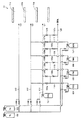
図1は、本発明の一実施の形態における気相成長装置としてのMOCVD装置の構成を示す断面図である。図2は、図1の原料ガス供給部付近の模式図である。図1および図2を参照して、本実施の形態におけるMOCVD装置1aは、反応室としてのチャンバ3と、サセプタ5と、ヒータ9と、原料ガス供給部11とを備えている。チャンバ3内にはサセプタ5とヒータ9と原料ガス供給部11とが配置されている。原料ガス供給部11は図1中横方向に延びており、原料ガス供給部11の内部にはサセプタ5の載置面(図1では上面)が面している。
FIG. 1 is a cross-sectional view showing a configuration of an MOCVD apparatus as a vapor phase growth apparatus according to an embodiment of the present invention. FIG. 2 is a schematic view of the vicinity of the source gas supply unit of FIG. Referring to FIGS. 1 and 2,
サセプタ5は、チャンバ3の内部に配置されている。このサセプタ5は円盤形状を有しており、同じく円盤形状を有するヒータ9上に配置されている。サセプタ5の下部には回転機構としての回転軸13が取り付けられており、これにより、サセプタ5は原料ガス供給部11の内部に載置面が面した状態で回転可能となっている。サセプタ5の載置面には平面的に見て円形状を有する複数の溝7が形成されている。これらの溝7の各々に主表面20aを有する基板20の各々が載置され、これにより基板20が加熱される。サセプタ5の載置面にはたとえば7つの溝7が形成されており、これらの溝7の各々に円形の基板20が載置される。ヒータ9は、サセプタ5を介して基板20を加熱する。
The
原料ガス供給部11は、チャンバ3に、基板20の主表面20aに沿った方向から原料ガスG1、G2を供給している。つまり、原料ガス供給部11は、基板20の主表面20aに原料ガスG1、G2およびガスG3で構成される反応ガスを流すための通路である。本実施の形態の原料ガス供給部11はサセプタ5の載置面に対して平行に延びており、原料ガスの流れ方向(図1中左側から右側へ向かう方向)に垂直な面で見ると矩形の断面形状を有している。また、原料ガス供給部11は横型三層流方式であり、上流側(図1中左側)に第1のガス供給部11aと、第2のガス供給部11bと、第3のガス供給部11cとを含んでいる。
The source
この第1のガス供給部11aは、基板20の主表面20aに垂直な方向Dにおいて主表面20aに近い側に位置している。第2のガス供給部11bは、基板20の主表面20aに垂直な方向Dにおいて第1のガス供給部11aより主表面20aから遠い側に位置している。第3のガス供給部11cは、基板20の主表面20aに垂直な方向Dにおいて第2のガス供給部11bより主表面20aから遠い側に位置している。つまり、サセプタ5の載置面と垂直な方向Dにおいて、第1のガス供給部11a、第2のガス供給部11b、第3のガス供給部11cの順に、サセプタ5の載置面に近い。なお、第1〜第3のガス供給部11a〜11cの原料ガスG1、G2およびガスG3の出口の位置は、基板20の主表面20aとに沿った方向、つまり原料ガスG1、G2およびガスG3の流れ方向において図1に示すように異なっていてもよく、同じであってもよい。
The first
第1のガス供給部11aは、V族元素を含む第1原料ガスとIII族元素を含む第2原料ガスとを含む原料ガスG1をチャンバ3に供給する。原料ガスG1として、NH3ガスなどのV族元素を含むガスと、H2ガス、N2ガスなどのキャリアガスとの混合ガスを用いることができる。第2のガス供給部11bは、III族元素を含む第3原料ガスを含む原料ガスG2をチャンバ3に供給する。原料ガスG2として、トリメチルガリウム(TMG)、トリメチルインジウム(TMI)、またはトリメチルアルミニウム(TMA)などのIII族元素を含む有機金属ガスと、H2ガス、N2ガスなどのキャリアガスとの混合ガスを用いることができる。第3のガス供給部11cは、原料を含まないガスG3を供給する。ガスG3は、原料ガスG1、G2の反応を抑制するパージガスが好適に用いられる。ガスG3として、H2ガス、N2ガスなどのキャリアガスを用いることができる。
The first
図2に示すように、原料ガス供給部11には、種々のガスを内部に収容する容器101〜107が配置されている。容器101は、NH3などV族元素を含む第1原料ガスである。容器102、103は、N2、H2などのキャリアガスである。容器104〜106は、それぞれTMG、TMI、TMAなどV族元素を含む第2および第3原料ガスである。容器107は、シクロペンタジエニルマグネシウム(Cp2Mg)などドーパントとなるガスである。なお、各原料ガス、キャリアガスおよびドーパントガスの配管には、流量を制御するためのマスフローコントローラーが設置されるが、図では省略されている。
As shown in FIG. 2, the source
原料ガス供給部11には、容器101〜103に収容されたガスを第1〜第3のガス供給部11a〜11cへそれぞれ供給するための配管111〜113が設けられている。
The source
容器104〜106の内部に収容されているIII族元素を含む第2および第3原料ガスを、第1および第2のガス供給部11a、11bへそれぞれ供給するために、容器104〜106に接続された分岐配管114〜116が設けられている。また容器107に収容されているドーパントガスを第1または第2のガス供給部11a、11bへそれぞれ供給するために、容器107に接続された分岐配管117が設けられている。この分岐配管114〜117は、第1および第2のガス供給部11a、11bにガスを供給するための配管111、112に接続されている。この分岐配管114〜117には、第1および第2のガス供給部11a、11b、およびベント配管120への供給を任意に選択するための切り替え部134a〜134c、135a〜135c、136a〜136c、137a〜137cが設けられている。なお、有機金属原料はキャリアガスを容器へ供給しバブリングさせて供給するが、容器の温度を一定に保つために恒温槽内で保持し容器内の圧力を一定に保つための圧力制御機構が設置される。これらは図では省略されている。
Connected to
図3は、本実施の形態の変形例におけるMOCVD装置の構成を示す断面図である。図3に示すように、MOCVD装置1bは、第3のガス供給部11cは省略されていてもよい。この場合に、チャンバ3の基板20の主表面20a(サセプタ5の載置面)と対向する面(図1において上壁)に原料ガスG1、G2が供給されることにより膜が堆積することを抑制するためのパージ機構などの手段が設けられていることが好ましい。
FIG. 3 is a cross-sectional view showing the configuration of the MOCVD apparatus in a modification of the present embodiment. As shown in FIG. 3, in the
なお、本実施の形態および変形例のMOCVD装置1a、1bでは、サセプタ5はチャンバ3の下方に配置されているフェースアップ方式であるが特にこれに限定されない。MOCVD装置は、チャンバ3の上方にサセプタ5が配置されているフェースダウン方式であってもよい。
In the
続いて、本実施の形態における気相成長方法としてのMOCVD法について説明する。本実施の形態では、図1および図2に示すMOCVD装置1aを用いて、MOCVD法によりIII−V族化合物半導体を成膜させる。
Next, the MOCVD method as the vapor phase growth method in this embodiment will be described. In the present embodiment, a group III-V compound semiconductor film is formed by MOCVD using the
まず、主表面20aを有する基板20を準備する。この工程では、たとえばMOCVD装置1aにおいて、サセプタ5の載置面に基板20が載置され、基板20をサセプタ5に保持させる。準備する基板20は特に限定されないが、たとえばGaN(窒化ガリウム)基板を用いることができる。
First, the
次に、基板20の主表面20aに沿った方向に原料ガスを供給しながら、基板20を加熱することにより基板20の主表面20aに膜を形成する。この膜を形成する工程では、基板20の主表面20aに垂直な方向Dにおいて主表面20aに近い側に位置する第1のガス供給部11aからV族元素を含む第1原料ガスとIII族元素を含む第2原料ガスとを含む原料ガスG1を基板20の主表面20a上に供給するとともに、基板20の主表面20aに垂直な方向Dにおいて第1のガス供給部11aより主表面20aから遠い側に位置する第2のガス供給部11bから、III族元素を含む第3原料ガスを含む原料ガスG2を基板20の主表面20a上に供給する。さらに、基板20の主表面20aに垂直な方向Dにおいて第2のガス供給部11bより主表面20aから遠い側に位置する第3のガス供給部11cから、原料を含まないガスG3を供給する。
Next, a film is formed on the
具体的には、MOCVD装置1aにおいては、サセプタ5の載置面に基板20が載置された状態で、ヒータ9によってサセプタ5が加熱され、回転軸13でサセプタ5が回転される。そして、第1〜第3のガス供給部11a〜11cの各々から原料ガスを構成する原料ガスG1、G2およびガスG3が導入される。原料ガスは上流側から下流側(図1中右方向)に流れていく。たとえばIII−V族化合物半導体層を成膜する場合、上述した原料ガスG1、G2が用いられる。これらの原料ガスG1、G2およびガスG3の各々が第1〜第3のガス供給部11a〜11cの各々へ導入されると、サセプタ5上において載置面に平行に導入されて拡散され、加熱されたサセプタ5により加熱される。第2および第3原料ガスに含まれるIII族元素を有するガスは加熱によって分解し中間反応体となり、同様に加熱によって分解した第1原料ガスに含まれるV族元素を有するガスの中間反応体と反応してIII−V族化合物半導体となる。その結果、III−V族化合物半導体が基板20の主表面20aに成膜される。
Specifically, in the
この膜を形成する工程では、第2原料ガスに含まれるIII族元素と、第3原料ガスに含まれるIII族元素とが同一であることが好ましい。たとえばIII族元素としてInを含むガスが第2および第3原料ガスに含まれている。この場合、Inを含むガスは同じであっても異なっていてもよい。異なっている場合には、Inを含むガスとしてTMIおよびトリエチルインジウム(TEI)などを用いることができる。また図2に示すような分岐配管114〜116および切り替え部134a、134b、135a、135b、136a、136bにより、第2および第3原料ガスを供給することができる。
In the step of forming this film, the group III element contained in the second source gas and the group III element contained in the third source gas are preferably the same. For example, a gas containing In as a group III element is contained in the second and third source gases. In this case, the gas containing In may be the same or different. If they are different, TMI and triethylindium (TEI) can be used as the gas containing In. Further, the second and third source gases can be supplied by the
また膜を形成する工程では、第2原料ガスに含まれるIII族元素の種類は、第3原料ガスに含まれるIII族元素の種類よりも少なくてもよい。たとえば、第1のガス供給部11aから1種類のIII族元素を含む第2原料ガスを供給し、第2のガス供給部11bから2種類以上のIII族元素を含む第3原料ガスを供給する。この場合、たとえば図2に示す切り替え部134a、134b、135a、136b、137a、137bにより、原料ガスのうち、容器104に収容されているTMGを第2のガス供給部11bのみに供給し、容器105に収容されているTMIを第1および第2のガス供給部11a、11bに供給する。
In the step of forming the film, the number of group III elements contained in the second source gas may be smaller than the type of group III elements contained in the third source gas. For example, a second source gas containing one group III element is supplied from the first
また膜を形成する工程では、第2原料ガスは第3原料ガスよりも熱分解しやすいことが好ましい。ここで、熱分解しやすいことは、たとえばダングリングボンドを有するIII族元素(活性III族元素)に分解されるために要する活性化エネルギーを値により判断することができる。たとえばTMG(Ga(CH3)3)とトリエチルガリウム(TEG:Ga(C2H5)3)とを比較する。Ga(CH3)3→Ga(CH3)2+CH3の反応に要する活性化エネルギーは59.5kcalであり、Ga(C2H5)3→Ga(C2H5)2+C2H5の反応に要する活性化エネルギーは47kcalである。このため、TEGの方がTMGよりも熱分解しやすい。またTMA(Al(CH3)3)とトリエチルアルミニウム(TEA:Al(C2H5)3)とを比較する。Al(CH3)3→Al(CH3)2+CH3の反応に要する活性化エネルギーは37.9kcalであり、Al(C2H5)3→Al(C2H5)2+C2H5の反応に要する活性化エネルギーは29kcalである。このため、TEAの方がTMAよりも熱分解しやすい。したがって、GaまたはAlを含む膜を形成する場合には、第1のガス供給部11aからTEG、TEAを供給し、第2のガス供給部11bからTMG、TMAを供給する。また、Inを含む膜を形成する場合には、第1のガス供給部11aからTEI(トリエチルインジウム)を供給し、第2のガス供給部11bからTMIを供給する。
In the step of forming a film, it is preferable that the second source gas is more easily pyrolyzed than the third source gas. Here, it is easy to thermally decompose, for example, the activation energy required for decomposing into a group III element (active group III element) having a dangling bond can be determined from the value. For example, TMG (Ga (CH 3 ) 3 ) and triethylgallium (TEG: Ga (C 2 H 5 ) 3 ) are compared. The activation energy required for the reaction of Ga (CH 3 ) 3 → Ga (CH 3 ) 2 + CH 3 is 59.5 kcal, Ga (C 2 H 5 ) 3 → Ga (C 2 H 5 ) 2 + C 2 H 5 The activation energy required for this reaction is 47 kcal. For this reason, TEG is easier to thermally decompose than TMG. The TMA (Al (CH 3) 3 ) and triethylaluminum (TEA: Al (C 2 H 5) 3) is compared with. The activation energy required for the reaction of Al (CH 3 ) 3 → Al (CH 3 ) 2 + CH 3 is 37.9 kcal, and Al (C 2 H 5 ) 3 → Al (C 2 H 5 ) 2 + C 2 H 5 The activation energy required for this reaction is 29 kcal. For this reason, TEA is easier to thermally decompose than TMA. Therefore, when forming a film containing Ga or Al, TEG and TEA are supplied from the first
また、上述したように第2原料ガスに含まれるIII族元素の種類は、第3原料ガスに含まれるIII族元素の種類よりも少ない場合には、第2および第3原料ガスの熱分解しやすさを考慮して第2および第3原料ガスを決定することが好ましい。この場合、形成する膜のIII族元素の組成の分布を制御できる。 In addition, as described above, when the number of group III elements contained in the second source gas is smaller than the type of group III elements contained in the third source gas, the second and third source gases are pyrolyzed. It is preferable to determine the second and third source gases in consideration of ease. In this case, the distribution of the composition of the group III element of the film to be formed can be controlled.
膜としてAlxGayIn(1-x-y)N(0≦x≦1、0≦y≦1、0≦x+y≦1)を形成することが好ましく、AlxGayN(0<x<1、0<y<1、x+y=1)、GayIn(1-y)N(0<y<1)およびAlxIn(1-x)N(0<x<1)のいずれかを形成することがより好ましく、GayIn(1-y)N(0<y<1)を形成することが最も好ましい。GayIn(1-y)N(0<y<1)を形成する場合には、第1のガス供給部11aからTMIを供給し、第2のガス供給部11bからTMGとTMIとを供給することが好ましい。また原料ガスG1、G2と同時にドーパントガスを基板20の主表面20aに供給することにより、ドーパントを含む膜を形成することもできる。
It is preferable to form Al x Ga y In (1-xy) N (0 ≦ x ≦ 1, 0 ≦ y ≦ 1, 0 ≦ x + y ≦ 1) as the film, and Al x Ga y N (0 <x <1). , 0 <y <1, x + y = 1), Ga y In (1-y) N (0 <y <1) and Al x In (1-x) N (0 <x <1) it is more preferable to, it is most preferable to form the Ga y In (1-y) N (0 <y <1). When forming a Ga y In (1-y) N (0 <y <1) supplies the TMI from the first
以上の工程を実施することにより、膜を形成することができる。本実施の形態では、サセプタ5に載置された基板20の主表面20aに垂直な方向Dにおいて主表面20aに近い側に位置する第1のガス供給部11aからV族元素を含む第1原料ガスとIII族元素を含む第2原料ガスとを含む原料ガスG1を基板20の主表面20a上に供給している。これにより、III族元素を含む第3原料ガスが第1のガス供給部11aから供給される原料ガスG1を拡散して基板20の主表面20aに到達する従来の場合と比較して、III族元素を含む第2原料ガスが上流側に位置する基板20の主表面20aまで拡散する距離を短くすることができる。このため、上流側でのIII族元素を含む第2原料ガスの濃度を高めることができ、上流側に位置する基板20の主表面20aに第2原料ガスを十分に供給することができる。また、第2のガス供給部11bからIII族元素を含む第3原料ガスも供給しているため、下流側に位置する基板20の主表面20aにもIII族元素を含む第3原料ガスを十分に供給することができる。したがって、上流から下流にかけて基板20の主表面20aに供給されるIII族原料の濃度を均一に供給できる。その結果、成膜される膜、特に複数の基板20上に膜を成膜させる場合には、複数の膜間のIII族元素の組成(組成比、モル比)の差を低減できる。よって、成膜される膜の組成を均一にすることができる。
By performing the above steps, a film can be formed. In the present embodiment, the first raw material containing the group V element from the first
このように成膜される膜の組成を均一にできると、平均として取り込まれるIII族元素の組成を確保することができる。このため、下流側(サセプタ5を回転させる場合には外周側)で過剰にIII族元素が取り込まれることを抑制することができる。これにより、III族元素の組成の値が必要以上に大きくなることに起因した膜の結晶性の劣化を抑制することができる。特にInの組成(1−y)が大きなGayIn(1-y)N(0<y<1)を成膜させる場合には、下流側(サセプタ5を回転させる場合には外周側)で、Inの組成(1−y)の値が目標とする値よりも大きくなることを抑制できる。このため、形成するGayIn(1-y)Nの結晶性を良好にできる傾向がある。
If the composition of the film thus formed can be made uniform, the composition of the group III element incorporated as an average can be ensured. For this reason, it is possible to prevent the group III element from being excessively taken in on the downstream side (the outer peripheral side when the
さらに、基板20に近い側である第1のガス供給部11aからV族元素、特にN源を供給している。このため、成膜する膜質が良好になる。
Further, a group V element, particularly an N source, is supplied from the first
さらには、上流側から十分な量のIII族元素とV族元素とを基板20に供給することができるので、従来よりも成膜が促進される。その結果として、成膜速度を向上することができる。
Furthermore, since a sufficient amount of group III element and group V element can be supplied to the
なお、本実施の形態ではMOCVD装置を用いてMOCVD法によりIII−V族化合物半導体膜を成膜させたが、特にこれに限定されない。たとえば、HVPE(Hydride Vapor Phase Epitaxy:ハイドライド気相成長)法などの気相成長法を採用することもできる。 Note that in this embodiment mode, a III-V compound semiconductor film is formed by MOCVD using an MOCVD apparatus, but the present invention is not limited to this. For example, a vapor phase growth method such as HVPE (Hydride Vapor Phase Epitaxy) method may be employed.
本実施例では、基板20の主表面20aに近い側に位置する第1のガス供給部11aからV族元素を含む第1原料ガスとIII族元素を含む第2原料ガスとを含む原料ガスG1を基板20の主表面20a上に供給することの効果について調べた。
In this embodiment, a source gas G1 containing a first source gas containing a group V element and a second source gas containing a group III element from the first
(本発明例1)
本発明例1では、基本的に上述した図1に示すMOCVD装置1aを用いてGayIn(1-y)N(0<y<1)を形成した。
(Invention Example 1)
In the present invention Example 1 to form a Ga y In (1-y) N (0 <y <1) with a
具体的には、まず、図1に示すMOCVD装置1aのサセプタ5の載置面において中心よりも上流側と中心よりも下流側とに基板20をそれぞれ載置した。なお、基板20は、サファイア基板上にGaNを1.5μm成膜したエピタキシャル基板を事前に準備した。
Specifically, first, the
次に、基板20の主表面20aに近い側から順に原料ガスG1、G2およびガスG3を下記の表1に示す条件で供給しながら、サセプタ5が750℃になるようにヒータ9で加熱した。なお、回転軸13によりサセプタ5を回転させなかった。成長圧力を100kPaとして、基板20の主表面20a上にGayIn(1-y)Nを形成した。
Next, while the source gases G1, G2 and G3 were supplied in order from the side close to the
なお、第1のガス供給部11aから供給される原料ガスG1は、第1原料ガスとしてのNH3と、第2原料ガスとしてのTMIと、キャリアガスとしてのN2とであった。第2のガス供給部11bから供給される原料ガスG2は、第3原料ガスとしてのTMGおよびTMIと、キャリアガスとしてのN2とであった。第3のガス供給部11cから供給されるガスG3は、N2であった。第1のガス供給部11aから供給される原料ガスG1の流量は30slmであり、第2のガス供給部11bから供給される原料ガスG2の流量は15slmであった。第3のガス供給部11cから供給されるガスG3の流量は35slmであった。
The source gas G1 supplied from the first
第1および第2のガス供給部11a、11bから供給される原料ガスG1、G2中の合計のTMIの供給量に対する第1のガス供給部11aから供給される原料ガスG1中のTMIの供給量{原料ガスG1のTMI/(原料ガスG1のTMI+原料ガスG2のTMI)}は、22%であった。また、原料ガスG1、G2中の合計のTMIと、原料ガスG2中のTMGとの合計の供給量に対する原料ガスG1、G2中の合計のTMIの供給量{TMI/(TMI+TMG)}は、54%であった。第1および第2のガス供給部11a、11bから供給される原料ガスG1、G2においてIII族元素に対するV族元素の比率(V/III)は12300であった。
The supply amount of TMI in the source gas G1 supplied from the first
(比較例1)
比較例1は、基本的には本発明例1と同様に成膜したが、第1および第2のガス供給部11a、11bから供給する原料ガスG1、G2が異なっていた。つまり、第1のガス供給部11aからはIII族元素を含む原料ガスを供給しなかった。
(Comparative Example 1)
Comparative Example 1 was basically formed in the same manner as Example 1 of the present invention, but the source gases G1 and G2 supplied from the first and second
具体的には、第1のガス供給部11aから供給する原料ガスは、NH3およびN2であった。第2のガス供給部11bから供給される原料ガスは、TMG、TMIと、N2とであった。第3のガス供給部11cから供給されるガスは、N2であった。第1のガス供給部11aから供給される原料ガスの流量は30slmであり、第2のガス供給部11bから供給される原料ガスの流量は15slmであった。第3のガス供給部11cから供給されるガスの流量は35slmであった。第2のガス供給部11bから供給される原料ガスにおいて、TMIとTMGとの合計の供給量に対するTMIの供給量{TMI/(TMI+TMG)}は、54%であった。第1および第2のガス供給部11a、11bから供給される原料ガスにおいてIII族元素に対するV族元素の比率(V/III)は16000であった。
Specifically, the source gases supplied from the first
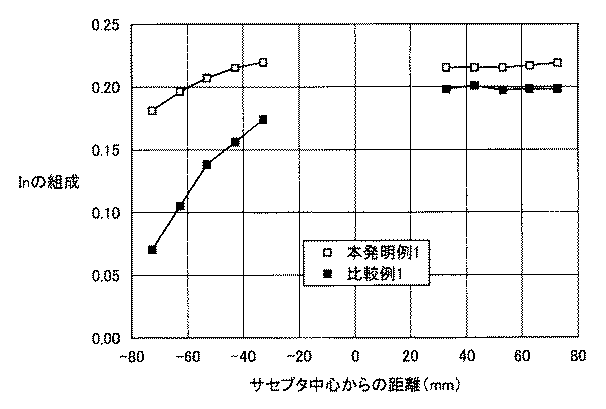
(評価方法)
本発明例1および比較例1の上流側および下流側の基板について、サセプタ5の中心からの距離を測定した。またそれぞれの基板上に成膜した膜のInの組成(1−y)をX線回折により測定した。その結果を図4に示す。なお、図4は、実施例1において基板の位置と、Inの組成との関係を示す図である。図4中、縦軸はインジウムの組成(単位:なし)を示し、横軸は、サセプタ5の中心から上流側に向けてマイナスとし、サセプタ5の中心から下流側に向けてプラスとしたときのサセプタ5の中心からの距離(単位:mm)を示す。
(Evaluation methods)
The distance from the center of the
(評価結果)
図4に示すように、第1のガス供給部11aからIII族元素を含む第2原料ガスを含む原料ガスG1が供給された本発明例1では、上流側の基板上の膜のInの組成(1−y)と、下流側の基板上の膜のInの組成(1−y)との差は、比較例1よりも小さくなっていた。このため、上流側と下流側との膜の組成の均一性を向上できた。
(Evaluation results)
As shown in FIG. 4, in Inventive Example 1 in which the source gas G1 containing the second source gas containing the group III element is supplied from the first
また、上流側の基板上の膜において、上流側に位置する領域のInの組成(1−y)と下流側に位置する領域のInの組成(1−y)との差は、比較例1よりも小さくなっていた。このため、膜の面内のInの組成の分布の差を緩和することができた。 Further, in the film on the upstream substrate, the difference between the In composition (1-y) in the region located upstream and the In composition (1-y) in the region located downstream is Comparative Example 1. It was smaller than. For this reason, the difference in the composition distribution of In in the plane of the film could be reduced.
本実施例では、基板20の主表面20aに近い側に位置する第1のガス供給部11aからV族元素を含む第1原料ガスとIII族元素を含む第2原料ガスとを含む原料ガスG1を基板20の主表面20a上に供給することの効果について調べた。
In this embodiment, a source gas G1 containing a first source gas containing a group V element and a second source gas containing a group III element from the first
(本発明例2)
本発明例2は、サセプタ5の上流側に1枚の基板を載置し、本発明例1と同様に成膜したが、回転軸13によりサセプタ5を回転しながら成膜した点、およびサセプタの温度が800℃であった点においてのみ異なっていた。
(Invention Example 2)
In the present invention example 2, a single substrate was placed on the upstream side of the
(本発明例3)
本発明例3は、サセプタ5の上流側に1枚の基板を載置し、基本的には本発明例2と同様に成膜したが、第1のガス供給部から供給した原料ガスG1中のTMIの供給量が下記の表2に示すように異なっていた。
(Invention Example 3)
In Invention Example 3, a single substrate is placed on the upstream side of the
具体的には、第1および第2のガス供給部11a、11bから供給される原料ガスG1、G2中のTMIの合計の供給量に対する第1のガス供給部11aから供給される原料ガスG1中のTMIの供給量{原料ガスG1のTMI/(原料ガスG1のTMI+原料ガスG2のTMI)}は、28%であった。その結果、原料ガスG1、G2中の合計のTMIと原料ガスG2中のTMGとの合計の供給量に対する原料ガスG1、G2中の合計のTMIの供給量{TMI/(TMI+TMG)}は、60%であった。第1および第2のガス供給部11a、11bから供給される原料ガスG1、G2においてIII族元素に対するV族元素の比率(V/III)は14700であった。
Specifically, in the source gas G1 supplied from the first
(比較例2)
比較例2は、サセプタ5の上流側に1枚の基板を載置し、基本的には比較例1と同様に成膜したが、回転軸13によりサセプタ5を回転しながら成膜した点、およびサセプタの温度が800℃であった点、および第1および第2のガス供給部11a、11bから供給される原料ガスにおいてIII族元素に対するV族元素の比率(V/III)は12800であった点においてのみ異なっていた。
(Comparative Example 2)
In Comparative Example 2, one substrate was placed on the upstream side of the
(比較例3)
比較例3は、サセプタ5の上流側に1枚の基板を載置し、基本的には比較例2と同様に成膜したが、第1のガス供給部から供給した原料ガス中のTMIの供給量が下記の表2に示すように異なっていた。具体的には、第2のガス供給部11bから供給される原料ガスにおいてTMIとTMGとの合計の供給量に対するTMIの供給量{TMI/(TMI+TMG)}は、60%であった。第1および第2のガス供給部11a、11bから供給される原料ガスにおいてIII族元素に対するV族元素の比率(V/III)は14700であった。
(Comparative Example 3)
In Comparative Example 3, a single substrate was placed on the upstream side of the
なお、比較例2および3のそれぞれのInの総供給量は、本発明例2および3のそれぞれのInの総供給量と同じであった。 The total supply amount of In in Comparative Examples 2 and 3 was the same as the total supply amount of In in Invention Examples 2 and 3.
(評価方法)
本発明例2、3および比較例2、3の基板上に成膜した各々の膜について、実施例1と同様にInの組成(1−y)を測定した。その結果を図5に示す。なお、図5は、実施例2におけるIII族元素の原料中のTMIと、膜のInの組成との関係を示す図である。図5中、縦軸はインジウムの組成(単位:なし)を示し、横軸は原料中のIII族元素の原料であるTMIとTMGとの合計に対するTMIの割合(単位:%)を示す。
(Evaluation methods)
For each of the films formed on the substrates of Invention Examples 2 and 3 and Comparative Examples 2 and 3, the In composition (1-y) was measured in the same manner as in Example 1. The result is shown in FIG. FIG. 5 is a diagram showing the relationship between the TMI in the Group III element raw material and the In composition of the film in Example 2. In FIG. 5, the vertical axis represents the composition of indium (unit: none), and the horizontal axis represents the ratio (unit:%) of TMI to the total of TMI and TMG, which are raw materials of group III elements in the raw material.
(評価結果)
図5に示すように、本発明例2、3は、比較例2、3に比較して、Inの供給源であるTMIの供給量が同じにも関わらず、Inの組成(1−y)が高いGayIn(1-y)Nを成膜することができた。つまり、基板20の主表面20aに近い側に位置する第1のガス供給部11aからV族元素を含む第1原料ガスとIII族元素を含む第2原料ガスとを含む原料ガスG1を基板20の主表面20a上に供給することにより、Inの取り込み量を増加できることがわかった。
(Evaluation results)
As shown in FIG. 5, Inventive Examples 2 and 3 have a composition of In (1-y) in comparison with Comparative Examples 2 and 3, even though the supply amount of TMI as an In supply source is the same. We were able to deposit a high Ga y In (1-y) N. That is, the source gas G1 containing the first source gas containing the group V element and the second source gas containing the group III element from the first
本実施例では、基板20の主表面20aに近い側に位置する第1のガス供給部11aからV族元素を含む第1原料ガスとIII族元素を含む第2原料ガスとを含む原料ガスG1を基板の主表面上に供給することの効果について調べた。
In this embodiment, a source gas G1 containing a first source gas containing a group V element and a second source gas containing a group III element from the first
(本発明例4)
本発明例4は、サセプタ5の上流側に1枚の基板を載置し、基本的には本発明例1と同様に成膜したが、以下の点が異なっていた。
(Invention Example 4)
In Example 4 of the present invention, a single substrate was placed on the upstream side of the
具体的には、サファイア基板上に1.5μmの厚みを有するGaN層を形成した。次に、下記の表3に示す条件でGayIn(1-y)N(0<y<1)を形成した。つまり、第1および第2のガス供給部11a、11bから供給される原料ガスG1、G2中の合計のTMIの供給量に対する第1のガス供給部11aから供給される原料ガスG1中のTMIの供給量{原料ガスG1のTMI/(原料ガスG1のTMI+原料ガスG2のTMI)}は、8.3%であった。その結果、原料ガスG1、G2中の合計のTMIと原料ガスG2中のTMGとの合計の供給量に対する原料ガスG1、G2中の合計のTMIの供給量{TMI/(TMI+TMG)}は、56%であった。第1および第2のガス供給部11a、11bから供給される原料ガスG1、G2においてIII族元素に対するV族元素の比率(V/III)は14000であった。
Specifically, a GaN layer having a thickness of 1.5 μm was formed on the sapphire substrate. Next, to form a Ga y In (1-y) N (0 <y <1) under the conditions shown in Table 3 below. That is, the TMI in the source gas G1 supplied from the first
(比較例4)
比較例4は、サセプタ5の上流側に1枚の基板を載置し、基本的には比較例1と同様に成膜したが、第1のガス供給部から供給した原料ガス中のTMIの供給量が下記の表3に示すように異なっていた。具体的には、第2のガス供給部11bから供給される原料ガスにおいてTMIとTMGとの合計の供給量に対するTMIの供給量{TMI/(TMI+TMG)}は、54%であった。第1および第2のガス供給部11a、11bから供給される原料ガスG1、G2においてIII族元素に対するV族元素の比率(V/III)は13100であった。
(Comparative Example 4)
In Comparative Example 4, a single substrate was placed on the upstream side of the
(評価方法)
本発明例4および比較例4の基板上に成膜した膜について、Inの組成(1−y)、膜厚、X線回折ピーク強度およびX線回折半値幅をそれぞれ測定した。Inの組成(1−y)は、実施例1と同様に測定した。
(Evaluation methods)
For the films formed on the substrates of Invention Example 4 and Comparative Example 4, the In composition (1-y), film thickness, X-ray diffraction peak intensity, and X-ray diffraction half width were measured. The In composition (1-y) was measured in the same manner as in Example 1.
また、ω−2θスキャンでは、ω(試料角度)と2θ(検出器角度)を同期させ測定を行った。ωスキャンでは、2θをInGaN結晶ピーク位置に固定し、ωをスキャンし測定を行った。その結果を図6および図7に示す。なお、図6および図7は、実施例3における回折強度を示す図である。図6および図7中、縦軸は回折強度(単位:カウント数/秒)を示し、横軸はω(単位:秒)を示す。図6において、ωが0(秒)の角度位置はGaN結晶を示し、−1500(秒)を示す角度位置はInGaN結晶を示す。図6において、回折強度のピーク値を示すωが大きいほど、Inの取り込み量が多いことを示す。この図6の縦軸のピーク値をX線回折ピーク強度として求めた。また、図7のピーク幅からX線回折半値幅を求めた。その結果を下記の表3に示す。 In the ω-2θ scan, measurement was performed by synchronizing ω (sample angle) and 2θ (detector angle). In the ω scan, 2θ was fixed at the InGaN crystal peak position, and ω was scanned for measurement. The results are shown in FIGS. 6 and 7 are diagrams showing diffraction intensities in Example 3. FIG. 6 and 7, the vertical axis represents diffraction intensity (unit: count / second), and the horizontal axis represents ω (unit: second). In FIG. 6, an angular position where ω is 0 (second) indicates a GaN crystal, and an angular position where −1500 (second) indicates an InGaN crystal. In FIG. 6, it is shown that the larger the value of ω that indicates the peak value of diffraction intensity, the greater the amount of In incorporated. The peak value on the vertical axis in FIG. 6 was determined as the X-ray diffraction peak intensity. Further, the X-ray diffraction half width was obtained from the peak width of FIG. The results are shown in Table 3 below.
(評価結果)
図6に示すように、第1のガス供給部11aからIII族元素を含む第2原料ガスを含む原料ガスG1が供給された本発明例4は、III族元素を含む原料を第2のガス供給部11bから供給した比較例4よりもInの取り込み量が多かった。これにより、本発明例4は比較例4よりも上流側でInを十分に取り込めたので、基板を回転させた場合の平均的な組成を向上できたことがわかった。
(Evaluation results)
As shown in FIG. 6, Example 4 of the present invention in which the source gas G1 containing the second source gas containing the group III element is supplied from the first
また図6および表3に示すように、本発明例4は比較例4よりもX線回折ピーク強度が高かった。これにより、本発明例4は比較例4よりもIn組成のばらつきが少なかったことがわかった。さらに図7および表3に示すように、本発明例4は比較例4よりもピーク値が高く、X線回折半値幅が狭かった。これにより、本発明例4は比較例4よりも結晶性が良好であったことがわかった。このため、第1のガス供給部11aからIII族元素を含む第2原料ガスを含む原料ガスG1が供給することで、膜の結晶性を向上できることがわかった。
As shown in FIG. 6 and Table 3, Example 4 of the present invention had higher X-ray diffraction peak intensity than Comparative Example 4. As a result, it was found that Inventive Example 4 had less variation in In composition than Comparative Example 4. Further, as shown in FIG. 7 and Table 3, Example 4 of the present invention had a peak value higher than that of Comparative Example 4 and a narrow X-ray diffraction half width. Thus, it was found that the inventive example 4 had better crystallinity than the comparative example 4. For this reason, it turned out that the crystallinity of a film | membrane can be improved by supplying the source gas G1 containing the 2nd source gas containing a III group element from the 1st
今回開示された実施の形態および実施例はすべての点で例示であって制限的なものではないと考えられるべきである。本発明の範囲は上記した実施の形態ではなくて特許請求の範囲によって示され、特許請求の範囲と均等の意味および範囲内でのすべての変更が含まれることが意図される。 It should be understood that the embodiments and examples disclosed herein are illustrative and non-restrictive in every respect. The scope of the present invention is shown not by the above-described embodiment but by the scope of claims for patent, and is intended to include all modifications within the meaning and scope equivalent to the scope of claims for patent.
1a,1b MOCVD装置、3 チャンバ、5 サセプタ、7 溝、9 ヒータ、11 原料ガス供給部、11a 第1のガス供給部、11b 第2のガス供給部、11c 第3のガス供給部、13 回転軸、20 基板、20a 主表面、101〜107 容器、111〜113 配管、114〜117 分岐配管、120 ベント配管、134a〜134c,135a〜135c,136a〜136c,137a〜137c 切り替え部、D 方向、G1,G2 原料ガス、G3 ガス。 1a, 1b MOCVD apparatus, 3 chamber, 5 susceptor, 7 groove, 9 heater, 11 source gas supply unit, 11a first gas supply unit, 11b second gas supply unit, 11c third gas supply unit, 13 rotations Axis, 20 substrate, 20a main surface, 101-107 container, 111-113 piping, 114-117 branch piping, 120 vent piping, 134a-134c, 135a-135c, 136a-136c, 137a-137c switching part, D direction, G1, G2 source gas, G3 gas.
Claims (12)
前記基板の前記主表面に沿った方向に原料ガスを供給しながら、前記基板を加熱することにより前記基板の前記主表面に膜を形成する工程とを備え、
前記膜を形成する工程では、
前記基板の前記主表面に垂直な方向において前記主表面に近い側に位置する第1のガス供給部からV族元素を含む第1原料ガスとIII族元素を含む第2原料ガスとを含む原料ガスを前記基板の前記主表面上に供給するとともに、
前記基板の前記主表面に垂直な方向において前記第1のガス供給部より前記主表面から遠い側に位置する第2のガス供給部から、III族元素を含む第3原料ガスを含む原料ガスを前記基板の前記主表面上に供給する、気相成長方法。 Preparing a substrate having a main surface;
Forming a film on the main surface of the substrate by heating the substrate while supplying a source gas in a direction along the main surface of the substrate,
In the step of forming the film,
A source material including a first source gas containing a group V element and a second source gas containing a group III element from a first gas supply unit located on the side close to the main surface in a direction perpendicular to the main surface of the substrate Supplying gas onto the main surface of the substrate;
A source gas containing a third source gas containing a group III element from a second gas supply unit located on a side farther from the main surface than the first gas supply unit in a direction perpendicular to the main surface of the substrate. A vapor phase growth method for supplying the main surface of the substrate.
前記第1および第2のガス供給部から前記原料ガスを供給するとともに、前記基板の前記主表面に垂直な方向において前記第2のガス供給部より前記主表面から遠い側に位置する第3のガス供給部から、原料を含まないガスをさらに供給する、請求項1に記載の気相成長方法。 In the step of forming the film,
The source gas is supplied from the first and second gas supply units, and a third position is located farther from the main surface than the second gas supply unit in a direction perpendicular to the main surface of the substrate. The vapor phase growth method according to claim 1, wherein a gas not containing a raw material is further supplied from a gas supply unit.
前記反応室の内部に配置される主表面を有する基板を載置するサセプタと、
前記サセプタを介して前記基板を加熱するヒータと、
前記反応室に、前記基板の前記主表面に沿った方向から原料ガスを供給する原料ガス供給部とを備え、
前記原料ガス供給部は、
前記基板の前記主表面に垂直な方向において前記主表面に近い側に位置し、V族元素を含む第1原料ガスとIII族元素を含む第2原料ガスとを含む原料ガスを前記反応室に供給する第1のガス供給部と、
前記基板の前記主表面に垂直な方向において前記第1のガス供給部より前記主表面から遠い側に位置し、III族元素を含む第3原料ガスを含む原料ガスを前記反応室に供給する第2のガス供給部とを含む、気相成長装置。 A reaction chamber;
A susceptor on which a substrate having a main surface disposed inside the reaction chamber is placed;
A heater for heating the substrate via the susceptor;
A source gas supply unit that supplies source gas from a direction along the main surface of the substrate in the reaction chamber,
The source gas supply unit
A source gas, which is located near the main surface in a direction perpendicular to the main surface of the substrate and includes a first source gas containing a group V element and a second source gas containing a group III element, is supplied to the reaction chamber. A first gas supply section for supplying;
A source gas containing a third source gas containing a group III element and located at a position farther from the main surface than the first gas supply unit in a direction perpendicular to the main surface of the substrate is supplied to the reaction chamber. And a gas supply unit.
前記第2および第3原料ガスとしてのIII族元素を含む原料を、前記第1および第2のガス供給部へそれぞれ供給するための分岐配管と、
前記分岐配管に設けられ、前記第1および第2のガス供給部への供給を選択するための切り替え部とをさらに含む、請求項10に記載の気相成長装置。 The source gas supply unit
Branch pipes for supplying a raw material containing a group III element as the second and third raw material gases to the first and second gas supply parts, respectively;
The vapor phase growth apparatus according to claim 10, further comprising: a switching unit provided in the branch pipe for selecting supply to the first and second gas supply units.
Priority Applications (1)
| Application Number | Priority Date | Filing Date | Title |
|---|---|---|---|
| JP2008232371A JP4835666B2 (en) | 2008-09-10 | 2008-09-10 | Vapor growth method |
Applications Claiming Priority (1)
| Application Number | Priority Date | Filing Date | Title |
|---|---|---|---|
| JP2008232371A JP4835666B2 (en) | 2008-09-10 | 2008-09-10 | Vapor growth method |
Publications (2)
| Publication Number | Publication Date |
|---|---|
| JP2010067775A true JP2010067775A (en) | 2010-03-25 |
| JP4835666B2 JP4835666B2 (en) | 2011-12-14 |
Family
ID=42193113
Family Applications (1)
| Application Number | Title | Priority Date | Filing Date |
|---|---|---|---|
| JP2008232371A Expired - Fee Related JP4835666B2 (en) | 2008-09-10 | 2008-09-10 | Vapor growth method |
Country Status (1)
| Country | Link |
|---|---|
| JP (1) | JP4835666B2 (en) |
Cited By (1)
| Publication number | Priority date | Publication date | Assignee | Title |
|---|---|---|---|---|
| JP2012216735A (en) * | 2011-04-01 | 2012-11-08 | Showa Denko Kk | Manufacturing method of semiconductor element |
Citations (5)
| Publication number | Priority date | Publication date | Assignee | Title |
|---|---|---|---|---|
| JPH04338636A (en) * | 1991-05-15 | 1992-11-25 | Furukawa Electric Co Ltd:The | Semiconductor vapor growth device |
| JPH0645264A (en) * | 1992-07-23 | 1994-02-18 | Nec Corp | Vapor growing method |
| JPH06132227A (en) * | 1992-10-16 | 1994-05-13 | Nec Corp | Vapor growth method |
| JP2008016609A (en) * | 2006-07-05 | 2008-01-24 | Sumitomo Electric Ind Ltd | Organometallic vapor deposition device |
| JP2008153357A (en) * | 2006-12-15 | 2008-07-03 | Sumitomo Electric Ind Ltd | Vapor deposition apparatus |
-
2008
- 2008-09-10 JP JP2008232371A patent/JP4835666B2/en not_active Expired - Fee Related
Patent Citations (5)
| Publication number | Priority date | Publication date | Assignee | Title |
|---|---|---|---|---|
| JPH04338636A (en) * | 1991-05-15 | 1992-11-25 | Furukawa Electric Co Ltd:The | Semiconductor vapor growth device |
| JPH0645264A (en) * | 1992-07-23 | 1994-02-18 | Nec Corp | Vapor growing method |
| JPH06132227A (en) * | 1992-10-16 | 1994-05-13 | Nec Corp | Vapor growth method |
| JP2008016609A (en) * | 2006-07-05 | 2008-01-24 | Sumitomo Electric Ind Ltd | Organometallic vapor deposition device |
| JP2008153357A (en) * | 2006-12-15 | 2008-07-03 | Sumitomo Electric Ind Ltd | Vapor deposition apparatus |
Cited By (1)
| Publication number | Priority date | Publication date | Assignee | Title |
|---|---|---|---|---|
| JP2012216735A (en) * | 2011-04-01 | 2012-11-08 | Showa Denko Kk | Manufacturing method of semiconductor element |
Also Published As
| Publication number | Publication date |
|---|---|
| JP4835666B2 (en) | 2011-12-14 |
Similar Documents
| Publication | Publication Date | Title |
|---|---|---|
| EP2084304B1 (en) | Method and apparatus for the epitaxial deposition of monocrystalline group iii-v semiconductor material using gallium trichloride | |
| US8133322B2 (en) | Apparatus for inverted multi-wafer MOCVD fabrication | |
| US20080050889A1 (en) | Hotwall reactor and method for reducing particle formation in GaN MOCVD | |
| US20100242835A1 (en) | High volume delivery system for gallium trichloride | |
| US20090223442A1 (en) | Methods for high volume manufacture of group iii-v semiconductor materials | |
| JP4840832B2 (en) | Vapor phase growth apparatus, vapor phase growth method, and semiconductor device manufacturing method | |
| WO2008064080A1 (en) | High volume delivery system for gallium trichloride | |
| EP2066496A2 (en) | Equipment for high volume manufacture of group iii-v semiconductor materials | |
| EP2083935A2 (en) | Abatement of reaction gases from gallium nitride deposition | |
| JP2021511440A (en) | Method for manufacturing graphene layer structure | |
| US9481943B2 (en) | Gallium trichloride injection scheme | |
| JP4466723B2 (en) | Metalorganic vapor phase epitaxy system | |
| TW201248695A (en) | Device and method for large-scale deposition of semi-conductor layers with gas-separated hcl-feeding | |
| US20100307418A1 (en) | Vapor phase epitaxy apparatus of group iii nitride semiconductor | |
| US20160194753A1 (en) | SiC-FILM FORMATION DEVICE AND METHOD FOR PRODUCING SiC FILM | |
| JP4835666B2 (en) | Vapor growth method | |
| JP5110074B2 (en) | Crystal manufacturing method and light emitting device manufacturing method | |
| JP4524175B2 (en) | Metal organic vapor phase growth apparatus and semiconductor manufacturing method | |
| US20130295283A1 (en) | Chemical vapor deposition apparatus with multiple inlets for controlling film thickness and uniformity | |
| JP7349341B2 (en) | Vapor phase growth apparatus and vapor phase growth method | |
| CN110662858B (en) | Method for supplying gases to grow epitaxial structures based on group III metal nitrides | |
| JP3472976B2 (en) | Method and apparatus for forming group III nitride semiconductor | |
| KR100988213B1 (en) | Device for manufacturing GaN substrate | |
| JP2002261021A (en) | Apparatus and method for vapor-phase growth | |
| US20120231609A1 (en) | Vapor-phase growing apparatus and vapor-phase growing method |
Legal Events
| Date | Code | Title | Description |
|---|---|---|---|
| A977 | Report on retrieval |
Free format text: JAPANESE INTERMEDIATE CODE: A971007 Effective date: 20110610 |
|
| A131 | Notification of reasons for refusal |
Free format text: JAPANESE INTERMEDIATE CODE: A131 Effective date: 20110621 |
|
| A521 | Written amendment |
Free format text: JAPANESE INTERMEDIATE CODE: A523 Effective date: 20110805 |
|
| TRDD | Decision of grant or rejection written | ||
| A01 | Written decision to grant a patent or to grant a registration (utility model) |
Free format text: JAPANESE INTERMEDIATE CODE: A01 Effective date: 20110830 |
|
| A01 | Written decision to grant a patent or to grant a registration (utility model) |
Free format text: JAPANESE INTERMEDIATE CODE: A01 |
|
| A61 | First payment of annual fees (during grant procedure) |
Free format text: JAPANESE INTERMEDIATE CODE: A61 Effective date: 20110912 |
|
| FPAY | Renewal fee payment (prs date is renewal date of database) |
Free format text: PAYMENT UNTIL: 20141007 Year of fee payment: 3 |
|
| R150 | Certificate of patent (=grant) or registration of utility model |
Free format text: JAPANESE INTERMEDIATE CODE: R150 |
|
| R250 | Receipt of annual fees |
Free format text: JAPANESE INTERMEDIATE CODE: R250 |
|
| LAPS | Cancellation because of no payment of annual fees |