JP2010064220A - Polishing device and polishing method - Google Patents
Polishing device and polishing method Download PDFInfo
- Publication number
- JP2010064220A JP2010064220A JP2008234991A JP2008234991A JP2010064220A JP 2010064220 A JP2010064220 A JP 2010064220A JP 2008234991 A JP2008234991 A JP 2008234991A JP 2008234991 A JP2008234991 A JP 2008234991A JP 2010064220 A JP2010064220 A JP 2010064220A
- Authority
- JP
- Japan
- Prior art keywords
- polishing
- target
- substrate
- vibration
- amplitude
- Prior art date
- Legal status (The legal status is an assumption and is not a legal conclusion. Google has not performed a legal analysis and makes no representation as to the accuracy of the status listed.)
- Granted
Links
Images


Abstract
Description
本発明は、膜が付された半導体ウェハなどの基板を研磨する研磨装置および研磨方法に関し、特に基板と研磨面との間に作用する摩擦の変化に基づいて研磨処理を制御する研磨装置および研磨方法に関する。 The present invention relates to a polishing apparatus and a polishing method for polishing a substrate such as a semiconductor wafer provided with a film, and in particular, a polishing apparatus and a polishing for controlling a polishing process based on a change in friction acting between a substrate and a polishing surface. Regarding the method.
半導体デバイスの製造工程では、ウェハ上に種々の材料が膜状に繰り返し形成され、積層構造を形成する。この積層構造を形成するためには、膜が形成されたウェハの表面を平坦にする技術が重要となっている。このようなウェハの表面を平坦化する一手段として、化学機械研磨(CMP)を行う研磨装置が広く用いられている。 In a semiconductor device manufacturing process, various materials are repeatedly formed in a film shape on a wafer to form a laminated structure. In order to form this laminated structure, a technique for flattening the surface of the wafer on which the film is formed is important. As one means for flattening the surface of such a wafer, a polishing apparatus that performs chemical mechanical polishing (CMP) is widely used.
この種の研磨装置は、一般に、研磨パッドが取り付けられた研磨テーブルと、ウェハを保持するトップリングと、研磨液を研磨パッド上に供給するノズルとを備えている。ノズルから研磨液を研磨パッド上に供給しながら、トップリングによりウェハを研磨パッドに押し付け、さらにトップリングと研磨テーブルとを相対移動させることにより、ウェハを研磨してその表面を平坦にする。研磨装置は、通常、研磨終点を検出する装置を備えている。 This type of polishing apparatus generally includes a polishing table to which a polishing pad is attached, a top ring that holds a wafer, and a nozzle that supplies a polishing liquid onto the polishing pad. While supplying the polishing liquid onto the polishing pad from the nozzle, the wafer is pressed against the polishing pad by the top ring, and the top ring and the polishing table are moved relative to each other to polish the wafer and flatten the surface. The polishing apparatus usually includes a device that detects the polishing end point.
上述した研磨終点検出装置の1つとして、研磨が異材質へ移行した際の研磨摩擦力の変化を検知する装置が知られている。ウェハは、半導体、導体、絶縁体などの異なる材料を含む積層構造を有している。摩擦係数は材料によって異なるため、研磨により膜が除去されてその下地層が表面に現われると、研磨摩擦力が変化する。したがって、研磨摩擦力の変化から、ある特定の膜が研磨により除去されたことを検知することができる。 As one of the polishing end point detection devices described above, there is known a device that detects a change in polishing friction force when polishing is shifted to a different material. The wafer has a laminated structure including different materials such as a semiconductor, a conductor, and an insulator. Since the friction coefficient varies depending on the material, the polishing frictional force changes when the film is removed by polishing and the underlying layer appears on the surface. Therefore, it can be detected from the change in the polishing friction force that a specific film has been removed by polishing.
ここで、研磨摩擦力の変化は通常次のように検出される。研磨摩擦力は研磨テーブルの回転中心から偏心した位置に作用するため、回転する研磨テーブルには研磨摩擦力は負荷トルクとして作用する。このため、研磨摩擦力は研磨テーブルに働くトルクとして検出することができる。ウェハを保持するトップリングについても同様に、研磨摩擦力をトルクとして検出することができる。研磨テーブルまたはトップリングを回転駆動させる手段が電動モータの場合には、トルクはモータに流れる電流として測定することができる。したがって、電流を電流計でモニターし、電流値に適当な信号処理を施すことによって研磨終点が検知される。 Here, the change in the abrasive friction force is usually detected as follows. Since the polishing friction force acts at a position eccentric from the rotation center of the polishing table, the polishing friction force acts as a load torque on the rotating polishing table. For this reason, the polishing friction force can be detected as a torque acting on the polishing table. Similarly, the polishing frictional force can be detected as torque for the top ring that holds the wafer. When the means for rotationally driving the polishing table or the top ring is an electric motor, the torque can be measured as a current flowing through the motor. Therefore, the polishing end point is detected by monitoring the current with an ammeter and applying appropriate signal processing to the current value.
しかしながら、研磨テーブルおよびトップリングは、それ自体がある程度の重さを有しているため、研磨摩擦力の変化に起因した電流の変化を精度よく検知することは難しい。また、この方法は、ウェハの表面全体に作用する研磨摩擦力の変化を検知するため、ウェハの表面内での局所的な研磨状態を検知することができない。最近では、複数の加圧機構によりウェハの複数の領域に対して独立して押圧することが可能なトップリングが開発されている。このトップリングは、ウェハの領域ごとの研磨の進行に基づいて各領域に対する押圧力を調整することが可能である。しかしながら、上述の検知方法は、このような局所的な押圧力の調整に寄与することができない。 However, since the polishing table and the top ring themselves have a certain weight, it is difficult to accurately detect a change in current caused by a change in the polishing frictional force. Further, since this method detects a change in the polishing friction force acting on the entire surface of the wafer, it cannot detect a local polishing state within the wafer surface. Recently, a top ring has been developed that can be independently pressed against a plurality of regions of a wafer by a plurality of pressure mechanisms. The top ring can adjust the pressing force for each region based on the progress of polishing for each region of the wafer. However, the detection method described above cannot contribute to the adjustment of such a local pressing force.
本発明は上述した事情に鑑みてなされたもので、膜の除去などの研磨の変移点を精度よく検知することができ、かつ基板の表面内の局所的な研磨状態を監視することができる研磨装置および研磨方法を提供することを目的とする。 The present invention has been made in view of the above-described circumstances. Polishing capable of accurately detecting a transition point of polishing such as film removal and monitoring a local polishing state in the surface of the substrate. An object is to provide an apparatus and a polishing method.
上述した目的を達成するために、本発明の一態様は、研磨面を有する研磨パッドが取り付けられる研磨テーブルと、基板を前記研磨面に押圧する基板保持部とを有し、前記研磨テーブルと前記基板保持部の相対移動により基板の表面を研磨する研磨装置であって、前記基板の表面に接触するターゲットと、前記ターゲットの振動の振幅および周波数の少なくとも一方を測定する振動測定部と、前記振動測定部によって測定された前記振幅および周波数の少なくとも一方に基づいて研磨処理を制御する制御部とを備えたことを特徴とする。 In order to achieve the above-described object, one embodiment of the present invention includes a polishing table to which a polishing pad having a polishing surface is attached, and a substrate holding unit that presses a substrate against the polishing surface. A polishing apparatus for polishing a surface of a substrate by relative movement of a substrate holding unit, a target that contacts the surface of the substrate, a vibration measuring unit that measures at least one of amplitude and frequency of vibration of the target, and the vibration And a control unit that controls a polishing process based on at least one of the amplitude and the frequency measured by the measurement unit.
本発明の好ましい態様は、前記制御部は、前記振幅および周波数の少なくとも一方が増加または減少して所定の値となったときに、研磨終点に達したと判断することを特徴とする。
本発明の好ましい態様は、前記基板保持部は、前記基板の複数の領域を独立に押圧する複数の押圧機構を有し、前記制御部は、前記振動測定部によって測定された前記振幅および周波数の少なくとも一方に基づいて、前記複数の押圧機構の押圧力を制御することを特徴とする。
本発明の好ましい態様は、前記研磨テーブルには、その上面で開口する液体室が設けられ、前記ターゲットは、前記液体室内に配置されていることを特徴とする。
In a preferred aspect of the present invention, the control unit determines that the polishing end point has been reached when at least one of the amplitude and frequency increases or decreases to a predetermined value.
In a preferred aspect of the present invention, the substrate holding unit has a plurality of pressing mechanisms that independently press a plurality of regions of the substrate, and the control unit has the amplitude and frequency measured by the vibration measuring unit. The pressing force of the plurality of pressing mechanisms is controlled based on at least one of them.
In a preferred aspect of the present invention, the polishing table is provided with a liquid chamber that opens on an upper surface thereof, and the target is disposed in the liquid chamber.
本発明の好ましい態様は、前記ターゲットは、内部に流体が封入された弾性バッグを備えることを特徴とする。
本発明の好ましい態様は、前記振動測定部は、前記弾性バッグの振動の振幅および周波数の少なくとも一方を測定することを特徴とする。
本発明の好ましい態様は、前記弾性バッグに供給される流体の圧力を調整する圧力調整機構をさらに備えたことを特徴とする。
本発明の好ましい態様は、前記振動測定部は、前記弾性バッグに封入された流体の圧力を測定する圧力センサであることを特徴とする。
In a preferred aspect of the present invention, the target includes an elastic bag in which a fluid is sealed.
In a preferred aspect of the present invention, the vibration measuring unit measures at least one of amplitude and frequency of vibration of the elastic bag.
In a preferred aspect of the present invention, the pressure sensor further includes a pressure adjusting mechanism for adjusting the pressure of the fluid supplied to the elastic bag.
In a preferred aspect of the present invention, the vibration measuring unit is a pressure sensor that measures the pressure of the fluid sealed in the elastic bag.
本発明の好ましい態様は、前記ターゲットは、前記基板の表面に接触する接触パッドをさらに有しており、前記接触パッドは、前記弾性バッグに取り付けられており、前記振動測定部は、前記接触パッドの振動の振幅および周波数の少なくとも一方を測定することを特徴とする。
本発明の好ましい態様は、前記弾性バッグは光透過性を有する材料から構成されており、前記弾性バッグを介して前記基板の表面の画像を取得する画像取得手段をさらに備えていることを特徴とする。
本発明の好ましい態様は、前記画像取得手段によって取得された画像から前記基板の表面の構造を解析する画像解析部をさらに備えていることを特徴とする。
本発明の好ましい態様は、前記ターゲットと前記基板との接触圧力を調整する接触圧力調整機構をさらに備えたことを特徴とする。
本発明の好ましい態様は、前記制御部は、前記接触圧力調整機構を介して前記接触圧力を一定に制御することを特徴とする。
本発明の好ましい態様は、前記振動測定部は、前記ターゲットの画像を取得する画像取得手段と、前記画像取得手段によって取得された画像から前記ターゲットの振動の振幅および周波数の少なくとも一方を解析する画像解析部とを備えていることを特徴とする。
In a preferred aspect of the present invention, the target further includes a contact pad that comes into contact with the surface of the substrate, the contact pad is attached to the elastic bag, and the vibration measuring unit includes the contact pad. And measuring at least one of amplitude and frequency of vibration.
In a preferred aspect of the present invention, the elastic bag is made of a light-transmitting material, and further includes image acquisition means for acquiring an image of the surface of the substrate through the elastic bag. To do.
In a preferred aspect of the present invention, the image processing apparatus further includes an image analysis unit that analyzes the structure of the surface of the substrate from the image acquired by the image acquisition unit.
In a preferred aspect of the present invention, a contact pressure adjusting mechanism for adjusting a contact pressure between the target and the substrate is further provided.
In a preferred aspect of the present invention, the control unit controls the contact pressure to be constant through the contact pressure adjusting mechanism.
In a preferred aspect of the present invention, the vibration measurement unit includes an image acquisition unit that acquires an image of the target, and an image that analyzes at least one of an amplitude and a frequency of the vibration of the target from the image acquired by the image acquisition unit. And an analysis unit.
本発明の好ましい態様は、前記振動測定部は、前記ターゲットに光を照射する投光部と、前記ターゲットで反射した光を受光する受光部と、前記受光部によって受光された光の強さを測定する測定部とを有することを特徴とする。
本発明の好ましい態様は、前記ターゲットは、前記研磨パッドの一部であることを特徴とする。
本発明の好ましい態様は、前記研磨パッドには切れ込み線が形成されており、前記ターゲットは、前記切れ込み線で囲まれた領域であることを特徴とする。
本発明の好ましい態様は、前記ターゲットを構成する前記研磨パッドの一部は、他の部分よりも厚さが薄い部分であることを特徴とする。
In a preferred aspect of the present invention, the vibration measurement unit includes: a light projecting unit that irradiates light to the target; a light receiving unit that receives light reflected by the target; and an intensity of light received by the light receiving unit. And a measuring unit for measuring.
In a preferred aspect of the present invention, the target is a part of the polishing pad.
In a preferred aspect of the present invention, a cut line is formed in the polishing pad, and the target is a region surrounded by the cut line.
In a preferred aspect of the present invention, a part of the polishing pad constituting the target is a part having a smaller thickness than other parts.
本発明の好ましい態様は、前記基板の表面に光を照射し、該基板から戻ってくる反射光の強度を測定する反射強度測定部をさらに備えたことを特徴とする。
本発明の好ましい態様は前記ターゲットが接触する基板の箇所と、前記反射強度測定部が光を照射する基板の箇所とは同一であることを特徴とする。
本発明の好ましい態様は、前記制御部は、前記振幅および周波数の少なくとも一方と、前記反射光の強度とを選択的に監視することを特徴とする。
本発明の好ましい態様は、前記研磨テーブルの振動の振幅および周波数の少なくとも一方を測定するリファレンス測定部をさらに備え、前記振動測定部は前記研磨テーブルに設けられ、前記制御部は、前記振動測定部の測定値から前記リファレンス測定部の測定値を除算することを特徴とする。
In a preferred aspect of the present invention, the apparatus further includes a reflection intensity measuring unit that irradiates the surface of the substrate with light and measures the intensity of reflected light returning from the substrate.
In a preferred aspect of the present invention, the location of the substrate in contact with the target is the same as the location of the substrate where the reflection intensity measuring unit irradiates light.
In a preferred aspect of the present invention, the control unit selectively monitors at least one of the amplitude and frequency and the intensity of the reflected light.
A preferred aspect of the present invention further includes a reference measurement unit that measures at least one of an amplitude and a frequency of vibration of the polishing table, the vibration measurement unit is provided in the polishing table, and the control unit is the vibration measurement unit The measured value of the reference measuring unit is divided from the measured value.
本発明の他の態様は、基板を基板保持部により保持し、研磨テーブルに取り付けられた研磨パッドの研磨面に基板を押圧し、前記基板保持部と前記研磨テーブルとを相対移動させて前記基板の表面を研磨し、研磨中に、前記基板の表面に接触するターゲットの振動の振幅および周波数の少なくとも一方を測定し、測定された前記振幅および周波数の少なくとも一方に基づいて研磨処理を制御することを特徴とする研磨方法である。 In another aspect of the present invention, the substrate is held by the substrate holding unit, the substrate is pressed against the polishing surface of the polishing pad attached to the polishing table, and the substrate holding unit and the polishing table are relatively moved to move the substrate. Polishing the surface of the substrate, measuring at least one of the amplitude and frequency of the vibration of the target contacting the surface of the substrate during the polishing, and controlling the polishing process based on at least one of the measured amplitude and frequency A polishing method characterized by the following.
本発明の好ましい態様は、前記振幅および周波数の少なくとも一方が増加または減少して所定の値となったときに、研磨終点に達したと判断することを特徴とする。
本発明の好ましい態様は、測定された前記振幅および周波数の少なくとも一方に基づいて、前記基板の複数の領域に対する押圧力を制御することを特徴とする。
本発明の好ましい態様は、前記ターゲットと前記基板との接触圧力を一定に維持しながら、前記ターゲットの振動の振幅および周波数の少なくとも一方を測定することを特徴とする。
本発明の好ましい態様は、研磨中に、前記基板の表面に光を照射し、該基板から戻ってくる反射光の強度を測定することを特徴とする。
本発明の好ましい態様は、前記ターゲットが接触する基板の箇所と、前記光を照射する基板の箇所とは同一であることを特徴とする。
本発明の好ましい態様は、前記振幅および周波数の少なくとも一方と、前記反射光の強度とを選択的に監視することを特徴とする。
In a preferred aspect of the present invention, when at least one of the amplitude and frequency increases or decreases to a predetermined value, it is determined that the polishing end point has been reached.
In a preferred aspect of the present invention, the pressing force for the plurality of regions of the substrate is controlled based on at least one of the measured amplitude and frequency.
In a preferred aspect of the present invention, at least one of an amplitude and a frequency of vibration of the target is measured while maintaining a constant contact pressure between the target and the substrate.
In a preferred aspect of the present invention, the surface of the substrate is irradiated with light during polishing, and the intensity of reflected light returning from the substrate is measured.
In a preferred aspect of the present invention, the location of the substrate in contact with the target and the location of the substrate to which the light is irradiated are the same.
In a preferred aspect of the present invention, at least one of the amplitude and frequency and the intensity of the reflected light are selectively monitored.
本発明の好ましい態様は、研磨中に、前記基板の表面の画像を取得し、前記画像から前記基板の表面の構造を解析することを特徴とする。
本発明の好ましい態様は、研磨中に、前記ターゲットの画像を取得し、前記画像から前記ターゲットの振動の振幅および周波数の少なくとも一方を解析することを特徴とする。
In a preferred aspect of the present invention, an image of the surface of the substrate is acquired during polishing, and the structure of the surface of the substrate is analyzed from the image.
In a preferred aspect of the present invention, an image of the target is acquired during polishing, and at least one of an amplitude and a frequency of vibration of the target is analyzed from the image.
基板の被研磨面に接触するターゲットの振動の振幅およびは周波数は、基板の表面を構成する膜や表面形状に依存して変化する。したがって、研磨中にターゲットの振動の振幅および/または周波数を監視することにより、膜の除去や表面の凹凸の除去を検知することができる。さらに、基板の表面内の複数の領域ごとに振幅および周波数を測定することができるので、領域ごとの研磨状態を検知することができる。したがって、検知された研磨状態に応じて調整された押圧力で基板の各領域を研磨することが可能となる。 The amplitude and frequency of the vibration of the target in contact with the surface to be polished of the substrate vary depending on the film constituting the surface of the substrate and the surface shape. Therefore, by monitoring the amplitude and / or frequency of the target vibration during polishing, it is possible to detect the removal of the film and the removal of the surface irregularities. Furthermore, since the amplitude and frequency can be measured for each of a plurality of regions in the surface of the substrate, the polishing state for each region can be detected. Therefore, each region of the substrate can be polished with a pressing force adjusted according to the detected polishing state.
以下、本発明の実施形態について図面を参照しながら説明する。
以下に説明では、同一または対応する要素には同一の符号を付して、その重複する説明を省略する。
図1は、本発明の原理を説明するための研磨装置の断面を示す模式図である。図1に示すように、この研磨装置は、研磨パッド1を保持する研磨テーブル2と、膜を有するウェハWを保持して研磨パッド1に押圧するトップリング3と、研磨パッド1に研磨液(スラリー)を供給する研磨液供給ノズル4とを備えている。研磨テーブル2は、その下方に配置されるモータ(図示せず)に連結されており、軸心周りに回転可能になっている。研磨パッド1は研磨テーブル2の上面に固定されている。
Hereinafter, embodiments of the present invention will be described with reference to the drawings.
In the following description, the same or corresponding elements are denoted by the same reference numerals, and redundant description thereof is omitted.
FIG. 1 is a schematic view showing a cross section of a polishing apparatus for explaining the principle of the present invention. As shown in FIG. 1, this polishing apparatus includes a polishing table 2 that holds a
研磨パッド1の上面1aは、ウェハWが摺接される研磨面を構成している。トップリング3は、トップリングシャフト6を介してモータ及び昇降シリンダ(図示せず)に連結されている。これにより、トップリング3は昇降可能かつトップリングシャフト6周りに回転可能となっている。このトップリング3の下面には、ウェハWが真空吸着等によって保持される。
An
トップリング3の下面に保持されたウェハWはトップリング3によって回転させられつつ、回転している研磨テーブル2上の研磨パッド1にトップリング3によって押圧される。ウェハWが研磨面1aと摺接する間、研磨液供給ノズル4から研磨パッド1の研磨面1aに研磨液が供給され、これによりウェハWと研磨パッド1との間に研磨液が存在した状態でウェハWが研磨される。ウェハWと研磨面1aとを相対移動させる機構は、研磨テーブル2およびトップリング3によって構成される。
The wafer W held on the lower surface of the
研磨パッド1には、研磨テーブル2および研磨パッド1と一体に回転するターゲット10が設けられている。このターゲット10の上面は研磨面1aと略同一平面内(好ましくは同一平面内)に位置しており、研磨テーブル2(研磨パッド1)の回転に伴ってウェハWの被研磨面に周期的に接触する。ターゲット10の下面は研磨テーブル2に対向している。ターゲット10の上面はウェハWとの接触面であり、その面積はウェハWの表面よりも小さい。ターゲット10は、研磨パッド1と同じ材料から構成されてもよく、または異なる材料から形成されてもよい。
The
図2(a)は研磨パッド1とトップリング3に保持されたウェハWとの位置を示す平面図であり、図2(b)はターゲット10がウェハWを横切る軌跡を示す図である。ターゲット10が配置される位置は、研磨テーブル2が回転するたびに、ターゲット10がウェハWの中心Crを通る位置である。図1に示すように、ターゲット10の下方には振動測定部11が設けられており、振動測定部11は制御部12に接続されている。振動測定部11はターゲット10の振動の大きさ、すなわち振幅および周波数の少なくとも一方を測定し、その測定値を制御部12に送るようになっている。
2A is a plan view showing the positions of the
トップリング3および研磨テーブル2(研磨パッド1)が回転すると、ターゲット10は周期的にウェハWに接触する。このとき、ターゲット10とウェハWとの摩擦によりターゲット10が振動する。振動測定部11は、ターゲット10の振動の大きさを測定し、その測定値を制御部12に送る。制御部12は、振動測定部11から送られてくる振幅および周波数の少なくとも一方を監視し、その値に基づいて研磨の変移点を検出する。
When the
ターゲット10の振動の振幅および周波数は、ウェハWの表面を構成する膜の材料および表面形状に依存する。これは、膜の材料および表面形状によって摩擦係数が異なるからである。これに加え、最近では、上層の膜は除去されやすく、その下層の膜は除去されにくい化学成分を有する研磨液を用いて研磨することが一般的となっている。このような研磨液を用いて研磨すると、上層膜が除去されて下層膜が表出すると、研磨レートが極端に低下する。このことは、研磨が上層膜から下層膜に移行した時点で、ウェハWと研磨面1aとの摩擦が変化することを意味する。このように摩擦が変化すると、ターゲット10の振動の大きさが変化する。このような原理から、制御部12は、研磨中の振幅および/または周波数の変化から研磨の変移点を検出することができる。なお、研磨の変移点とは、例えば、膜が除去された点や膜の表面の凹凸が平坦化された点などである。
The vibration amplitude and frequency of the
振動測定部11としては、変位センサや加速度センサなどを用いることができる。変位センサの例としては、三角測距式変位センサやマイケルソン型干渉計などが挙げられる。加速度センサの例としては、MEMS(Micro Electro Mechanical Systems)タイプの加速度センサが挙げられる。図3は振動測定部11として変位センサを研磨テーブル2内に配置した例を示す断面図である。図3に示すように、ターゲット10の下面には、下向きの斜面を有する変位変換部材15が固定されており、この変位変換部材15の斜面によりターゲット10の横方向の変位が縦方向の変位に変換される。振動測定部11は変位変換部材15の斜面の変位を測定することで、ターゲット10の横方向の変位、すなわちターゲット10の振動の振幅および周波数を測定する。
As the
図4は振動測定部11としてMEMSタイプの加速度センサを研磨テーブル2内に配置した例を示す断面図である。図4に示すように、ターゲット10の下面には加速度センサとしての振動測定部11が固定されている。振動測定部(加速度センサ)11はターゲット10と一体に移動し、ターゲット10の加速度を測定する。したがって、振動測定部11はターゲット10の加速度から振動の振幅および周波数を求めることができる。ただし、本発明はこれらのセンサに限られず、振動を計測することができる他の計器を用いることができる。
FIG. 4 is a cross-sectional view showing an example in which a MEMS type acceleration sensor is arranged in the polishing table 2 as the
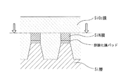
次に、上述した研磨装置をSTI(Shallow Trench Isolation)の形成に用いた例について説明する。図5はSTIの一工程を示す断面図であり、Si層に形成された凹凸構造上に絶縁膜であるSiO2膜が形成された積層構造を示している。図5に示すように、Si層(通常はシリコンウェハ)の凸部には、SiN膜(Si3N4)および熱酸化膜パッドが形成される。SiO2膜は、矢印で示すように、SiN膜が露出するまでCMP(化学機械研磨)により除去される。SiN膜はポリッシングストッパーとして機能し、CMPによってSi層がダメージを受けてしまうことを防止する。SiN膜はアクティブ部とも称される。 Next, an example in which the above-described polishing apparatus is used for forming STI (Shallow Trench Isolation) will be described. FIG. 5 is a cross-sectional view showing one step of the STI, and shows a laminated structure in which a SiO 2 film, which is an insulating film, is formed on the concavo-convex structure formed in the Si layer. As shown in FIG. 5, a SiN film (Si 3 N 4 ) and a thermal oxide film pad are formed on the convex portion of the Si layer (usually a silicon wafer). The SiO 2 film is removed by CMP (Chemical Mechanical Polishing) until the SiN film is exposed, as indicated by an arrow. The SiN film functions as a polishing stopper and prevents the Si layer from being damaged by CMP. The SiN film is also called an active part.
図6(a)は研磨の初期段階のSTI構造を示す断面図であり、図6(b)は図6(a)に示す状態のときに測定されたターゲット10の振動を示すグラフである。図6(b)において縦軸はターゲット10の変位を示し、横軸はターゲット10がウェハWを横切って移動している間の時間を示す。研磨の初期段階では、最上層の膜はSiO2膜であり、その表面には凹凸が形成されている。このときのターゲット10の振動の振幅は比較的小さく、一方で周波数は比較的高い。図7(a)は研磨がある程度進んだ状態のSTI構造を示す断面図であり、図7(b)は図7(a)に示す状態のときに測定されたターゲット10の振動を示すグラフである。図7(a)に示すように、最上層の膜であるSiO2膜の凹凸が除去されている。このときのターゲット10の振動の振幅は、図6(b)のグラフに比べて大きく、周波数は低い。このような波形の変化(すなわち振動の変化)は、図6(a)に示す表面状態と図7(a)に示す表面状態とでは摩擦が異なることに起因している。図6(a)および図7(a)に示す振動のグラフは、図6(a)に示す表面状態の方が図7(a)に示す表面状態よりも摩擦が小さいことを示している。つまり、この例では、摩擦は接触面積に比例していると考えられ、図6(a)ではSiO2膜の凸部のみの接触であることから、図7(a)に示す表面状態よりも摩擦が小さいと考えられる。
FIG. 6A is a cross-sectional view showing the STI structure in the initial stage of polishing, and FIG. 6B is a graph showing the vibration of the
図8(a)は研磨がさらに進んだ状態のSTI構造を示す断面図であり、図8(b)は図8(a)に示す状態のときに測定されたターゲット10の振動を示すグラフである。図8(a)および図8(b)は、研磨レートがウェハWの全面に亘って均一でない例を示している。すなわち、図8(a)に示すように、SiN膜の一部が表面に現われているが、SiN膜の中央部にはSiO2膜が残存している。このときのターゲット10の振動の振幅は、SiN膜が露出した領域では小さく、SiO2膜が残存している領域では大きい。一方、振動の周波数は、SiN膜が露出した領域では高く、SiO2膜が残存している領域では低い。
FIG. 8A is a cross-sectional view showing the STI structure in a state where the polishing is further advanced, and FIG. 8B is a graph showing the vibration of the
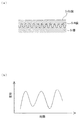
図9(a)は研磨終点に達したときのSTI構造を示す断面図であり、図9(b)は図9(a)に示す状態のときに測定されたターゲット10の振動を示すグラフである。研磨終点は、SiO2膜の下に形成されたSiN膜が表面に現われ、平坦な表面が形成された状態である。このときのターゲット10の振動の振幅は小さく、周波数は高い。図10は、図6(b)乃至図9(b)のグラフを研磨時間に沿って並べた図である。図10に示すように、研磨テーブル2の回転に伴って、ターゲット10がウェハWと周期的に接触し、摩擦によって振動していることが分かる。そして、ウェハWの表面を形成する膜の種類および表面形状によって、ターゲット10の振動の仕方が変わっている。
FIG. 9A is a cross-sectional view showing the STI structure when the polishing end point is reached, and FIG. 9B is a graph showing the vibration of the
このように、膜が除去されて、その下地層が現われると、ウェハWとターゲット10との間に作用する摩擦が変化し、その結果としてターゲット10の振動の振幅および周波数が変化する。したがって、振幅および周波数の少なくとも一方を監視することにより、膜が除去されたことを検出することができる。上述の積層構造の例では、SiO2膜が除去されると振幅が減少し、周波数が増加したが、膜の種類によっては、振幅の増加および周波数の減少が膜の除去を示すこともある。したがって、制御部12は、振幅が所定のしきい値にまで増加または低下したとき、および/または周波数が所定のしきい値にまで増加または低下したときに、膜が除去されたと判断する。
Thus, when the film is removed and the underlying layer appears, the friction acting between the wafer W and the
ところで、図8(a)に示すように、研磨レートがウェハWの全面に亘って均一でないと、膜の一部が除去されずに下地層の上に残存する。ターゲット10は、ウェハWの略径方向に沿ってウェハWの表面を横切るので、図8(b)のグラフの横軸は、研磨時間のみならず、ウェハWの径方向位置も表しているといえる。つまり、図8(b)のグラフの縦軸に示されるターゲット10の変位は、ウェハWの端から端まで連続的に測定され、振幅および周波数もウェハWの径方向の全体に亘って求められる。したがって、制御部12は、振幅および周波数の少なくとも一方から、残存する膜の位置(すなわち、研磨レートが低い領域)を特定することができる。さらに、制御部12は、研磨レートの低い領域に対する押圧力を高めるように、トップリング3に指令を出すことができる。
By the way, as shown in FIG. 8A, if the polishing rate is not uniform over the entire surface of the wafer W, a part of the film remains on the base layer without being removed. Since the
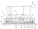
上述のような観点から、トップリング3は、ウェハWの複数の領域を独立に押圧する複数の押圧機構を有することが好ましい。図11は、そのような複数の押圧機構を有するトップリング3の一例を示す断面図である。トップリング3は、トップリングシャフト6に自由継手20を介して連結されるトップリング本体21と、トップリング本体21の下部に配置されたリテーナリング22とを備えている。トップリング本体21の下方には、ウェハWに当接する円形の弾性パッド(メンブレン)26と、弾性パッド26を保持するチャッキングプレート27とが配置されている。弾性パッド26とチャッキングプレート27との間には、4つの圧力室(エアバッグ)P1,P2,P3,P4が設けられている。圧力室P1,P2,P3,P4は弾性パッド26とチャッキングプレート27とによって形成されている。中央の圧力室P1は円形であり、他の圧力室P2,P3,P4は環状である。これらの圧力室P1,P2,P3,P4は、同心上に配列されている。
From the viewpoint as described above, the
圧力室P1,P2,P3,P4にはそれぞれ流体路31,32,33,34を介して圧力調整部40により加圧空気等の加圧流体が供給され、あるいは真空引きがされるようになっている。圧力室P1,P2,P3,P4の内部圧力は互いに独立して変化させることが可能であり、これにより、ウェハWの4つの領域、すなわち、中央部、内側中間部、外側中間部、および周縁部に対する押圧力を独立に調整することができる。また、トップリング3の全体を昇降させることにより、リテーナリング22を所定の押圧力で研磨パッド110に押圧できるようになっている。
Pressurized fluid such as pressurized air is supplied to the pressure chambers P1, P2, P3, and P4 by the
チャッキングプレート27とトップリング本体21との間には圧力室P5が形成され、この圧力室P5には流体路35を介して上記圧力調整部40により加圧流体が供給され、あるいは真空引きがされるようになっている。これにより、チャッキングプレート27および弾性パッド26全体が上下方向に動くことができる。ウェハWの周端部はリテーナリング22に囲まれており、研磨中にウェハWがトップリング3から飛び出さないようになっている。圧力室P3を構成する、弾性パッド26の部位には開口が形成されており、圧力室P3に真空を形成することによりウェハWがトップリング3に吸着保持されるようになっている。また、この圧力室P3に窒素ガスやクリーンエアなどを供給することにより、ウェハWがトップリング3からリリースされるようになっている。
A pressure chamber P5 is formed between the chucking
制御部12は、振動測定部11から送られてくる振幅および周波数の少なくとも一方の測定値に基づいて各圧力室P1,P2,P3,P4の内部圧力を決定し、決定された内部圧力が各圧力室P1,P2,P3,P4に形成されるように圧力調整部40に指令を出すようになっている。このような構成を有するトップリング3によれば、研磨レートが低い領域に対応する圧力室の内部圧力を高くすることにより、膜を均一に除去することができる。
The
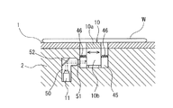
ターゲット10は振動測定部11に直接取り付けてもよく、または、図12に示すように、ばねやゴムなどの弾性部材を介して研磨テーブル2に連結してもよい。図12に示す例では、ターゲット10は、ウェハWに接触する接触パッド10aと、接触パッド10aを保持する台座10bとを有している。台座10bは、研磨テーブル2に形成された凹部45内に横方向に移動自在に置かれている。台座10bと凹部45の側面とはばね46により連結されており、ターゲット10に作用するばね46の横方向の力は釣り合っている。
The
振動測定部11は、研磨テーブル2に形成された部屋50内に配置されている。この部屋50は、凹部45の側面で開口しており、その開口は透明窓51によって塞がれている。振動測定部11としては、変位センサの一種であるレーザ干渉計が使用されている。部屋50の内部にはミラー52が配置されており、振動測定部(レーザ干渉計)11から発せられたレーザ光は、ミラー52で反射して透明窓51を通過し、ターゲット10の台座10bの側面に照射されるようになっている。台座10bの側面で反射したレーザ光は振動測定部11に戻り、これにより、ターゲット10の振動の大きさが振動測定部11によって測定される。なお、台座10bの側面のレーザ光が当たる箇所に、ミラーを取り付けてもよい。
The
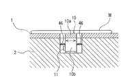
図13に示す図は、図12に示すターゲット10の変形例である。この例では、ばね46が上方に傾いており、これによりターゲット10に上向きの力が作用している。図14は、図12に示すターゲット10の他の変形例を示す断面図である。この例では、研磨テーブル2には、透明な液体としての純水が流れる液体供給路54および液体排出路55が形成されており、これら液体供給路54および液体排出路55は凹部45に連通している。この例では、凹部45は液体室として機能する。純水は、液体供給路54を通って凹部45に流入し、これにより凹部45は純水で満たされる。ターゲット10は、その上面を除き、純水中に浸漬される。液体は、凹部45に浸入した研磨液と共に、液体排出路55から排出される。このような構成によれば、研磨液(通常はスラリー)がターゲット10に付着することが防止され、ターゲット10の自由な動きが確保される。
The figure shown in FIG. 13 is a modification of the
図15は、図12に示すターゲット10のさらに他の変形例を示す断面図である。この例では、振動測定部11としてMEMSタイプの加速度センサが使用されている。振動測定部11はターゲット10の台座10bに取り付けられており、振動測定部11とターゲット10とは一体に振動するようになっている。
FIG. 15 is a cross-sectional view showing still another modification of the
上述の例では、ターゲット10は研磨パッド1から分離された部材として構成されているが、研磨パッド1の一部がターゲット10を構成してもよい。例えば、図16に示すように、研磨パッド1の一部をターゲット10と定義し、ターゲット10の下面(つまり研磨パッド1の下面)の振動を振動測定部11によって測定してもよい。この場合、研磨パッド1の一部の厚みを薄くして薄肉部を形成し、この薄肉部をターゲット10としてもよい。図17に示すように、研磨パッド1に環状の切れ込み線57を形成し、切れ込み線57で囲まれた領域をターゲット10としてもよい。なお、この場合の切れ込み線57は、複数のスリットが配列されて形成される線である。また、この場合、振動測定部11の測定精度を向上させるために、振動測定部11の一部を研磨パッド1に埋設してもよい。
In the above example, the
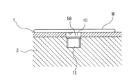
さらに、図18に示すように、ウェハWに接触する液体の振動の大きさを測定してもよい。図18に示す例では、研磨パッド1に形成されている貫通孔の下側開口部は薄いパッドなどの閉塞プレート58で塞がれている。貫通孔には液体が満たされており、この液体がターゲット10として機能する。液体の振動の大きさは閉塞プレート58を介して振動測定部11によって測定される。貫通孔を満たす液体は研磨液供給ノズル4から供給された研磨液でもよく、または純水などの他の液体でもよい。
Furthermore, as shown in FIG. 18, the magnitude of the vibration of the liquid that contacts the wafer W may be measured. In the example shown in FIG. 18, the lower opening of the through hole formed in the
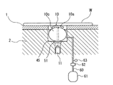
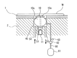
図19は、ターゲット10の他の例を示す断面図である。この例では、ターゲット10は、内部に流体が封入された弾性バッグ10cと、弾性バッグ10cの頂部に取り付けられた接触パッド10aとを有している。弾性バッグ10cは、研磨テーブル2に形成された凹部45内に配置されており、接触パッド10aは、研磨パッド1に形成された貫通孔の内部に位置しており、接触パッド10aの上面の少なくとも一部は、研磨パッド1の研磨面1aと略同一平面内に位置している。弾性バッグ10cは略円形の縦断面形状を有しており、弾力性のある樹脂などから構成されている。弾性バッグ10cには流体供給路60が接続され、この流体供給路60は流体供給源61に接続されている。空気や水などの流体は、流体供給源61から流体供給路60を通って弾性バッグ10cに供給される。流体供給路60には圧力調整機構62および圧力センサ63が設けられており、圧力調整機構62により弾性バッグ10c内の流体の圧力が調整され、圧力センサ63により弾性バッグ10c内の流体の圧力が測定される。圧力調整機構62の具体例としてはバルブが挙げられる。
FIG. 19 is a cross-sectional view showing another example of the
ターゲット10のウェハWに対する押圧力(すなわちターゲット10とウェハWとの接触圧力)は、弾性バッグ10c内の流体の圧力に依存する。ここで、ターゲット10のウェハWに対する押圧力は、振動の測定中、できるだけ一定に維持することが好ましい。そこで、本実施形態では、圧力センサ63の測定値が制御部12によって監視され、制御部12による接触圧力のフィードバック制御が行われている。より具体的には、制御部12は、圧力センサ63の測定値を監視し、この測定値と予め設定されている値との偏差がゼロとなるように圧力調整機構62を操作する。このようにして、制御部12は、振動測定部11による測定中、ターゲット10のウェハWに対する押圧力(接触圧力)が一定に維持されるようにフィードバック制御する。
The pressing force of the
上記設定値(すなわち、ターゲット10の押圧力の目標値)は、振動測定部11による振幅および/または周波数の測定が良好に行われる値に設定される。具体的には、被研磨面の状態や研磨装置の運転条件などに応じて上記設定値が決定される。被研磨面の状態としては、ウェハの種類や除去すべき膜の種類などが挙げられる。また、研磨装置の運転条件としては、研磨テーブル2の回転速度、研磨パッド1の種類、トップリング3によるウェハの研磨パッド1への押圧力、研磨パッド1の温度などが挙げられる。
The set value (that is, the target value of the pressing force of the target 10) is set to a value at which the measurement of the amplitude and / or frequency by the
上記設定値は制御部12に予め記憶される。また、ウェハの種類に対応した複数の設定値を制御部12に記憶することもできる。この場合は、ウェハの研磨開始時に、記憶されている複数の設定値からそのウェハに応じた設定値が選択される。このように、研磨対象となるウェハに関連づけられた押圧力でターゲット10がウェハに接触するので、より精度の高い振動測定が可能となっている。
The set value is stored in the
弾性バッグ10cは透明な材料から構成されている。接触パッド10aは弾性バッグ10cの頂部に取り付けられている。この接触パッド10aは、研磨パッド1と同じ材料から構成されてもよく、または別の材料から構成されてもよい。振動測定部11は弾性バッグ10cの下方に位置しており、接触パッド10aの下面に対向するように配置されている。より具体的には、弾性バッグ10cの下方に形成された孔の内部に振動測定部11が配置されている。孔の上端には研磨液などの液体の侵入を防ぐ透明窓51が設けられている。振動測定部11としては、変位センサの一種であるレーザ干渉計が用いられている。この振動測定部(レーザ干渉計)11は、レーザ光を弾性バッグ10cに向けて上方に発する。レーザ光は、弾性バッグ10cを貫通して接触パッド10aの下面で反射し、振動測定部11に戻る。弾性バッグ10cに供給される流体としては、空気や水などのレーザ光を透過させるものが選択される。
The
弾性バッグ10cの大きさは、流体の圧力によって変化する。したがって、研磨パッド1の摩耗に合わせて弾性バッグ10cの大きさを変更することにより、接触パッド10aの上面を研磨パッド1の研磨面1aと同一平面内に位置させることができる。接触パッド10aは、弾性体である弾性バッグ10cに保持されているので、ウェハWとの接触により振動する。振動測定部11は、接触パッド10aの振動の大きさを、弾性バッグ10cを貫通するレーザ光を用いて、弾性バッグ10cの下方から計測する。
The size of the
上述の構成において、接触パッド10aとウェハWとが接触すると、接触パッド10aと共に弾性バッグ10cが振動し、その内部に封入されている流体も振動する。したがって、圧力センサ63は、弾性バッグ10c内の流体の圧力を測定し、その圧力の変動からターゲット10(弾性バッグ10c)の振動の振幅および周波数を求めることができる。この場合は、圧力センサ63が振動測定部を構成する。なお、この場合は、上述の振動測定部11を省略してもよい。
In the above configuration, when the
図20は図19に示す構成の変形例を示す断面図である。この例では、研磨テーブル2に形成された凹部45に、上述した液体供給路54と液体排出路55が接続されている。純水は、液体供給路54を通じて凹部45に供給され、これにより凹部(すなわち液体室)45は純水で満たされる。そして、凹部45に侵入した研磨液は純水と共に液体排出路55を通じて排出される。その他の構成は図19に示す構成と同一である。
20 is a cross-sectional view showing a modification of the configuration shown in FIG. In this example, the
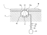
図21は図19に示す構成の他の変形例を示す断面図である。この例では、振動測定部11は、研磨テーブル2に形成された部屋50内に配置されている。この部屋50は、凹部45の側面で開口しており、その開口は透明窓51によって塞がれている。部屋50の内部にはミラー52が配置されており、振動測定部(レーザ干渉計)11から発せられたレーザ光は、ミラー52で反射して透明窓51を通過し、弾性バッグ10cの表面に照射されるようになっている。弾性バッグ10cの表面で反射したレーザ光は同じ経路をたどって振動測定部11に戻る。そして、振動測定部11は、接触パッド10aと一体に振動する弾性バッグ10cの振動の大きさを測定する。その他の構成は図19に示す構成と同一である。
FIG. 21 is a cross-sectional view showing another modification of the configuration shown in FIG. In this example, the
この例では、接触パッド10aを省略してもよい。この場合は、弾性バッグ10cがウェハWの表面に直接接触する。弾性バッグ10cは研磨パッド1と同じ材料で構成してもよい。また、図20に示す液体供給路54および液体排出路55を設けてもよい。この場合は、凹部45に供給される純水の流れによって弾性バッグ10cが振動しないように、測定中は純水の供給を止めるか、または純水の流量を低くすることが好ましい。
In this example, the
図22は図19に示す構成の他の変形例を示す断面図である。この例では、振動測定部11として、超音波式変位センサが使用されている。この振動測定部(超音波式変位センサ)11は弾性バッグ10cの下部に接するように配置されており、超音波を弾性バッグ10cに向けて上方に発する。超音波は、弾性バッグ10cを貫通して接触パッド10aの下面で反射し、振動測定部11に戻る。このように、振動測定部11は、接触パッド10aの振動の大きさを、弾性バッグ10cを貫通する超音波を用いて、弾性バッグ10cの下方から計測する。弾性バッグ10cに供給される流体としては、水などの液体が選択される。その他の構成は図19に示す構成と同一である。なお、図20に示す液体供給路54および液体排出路55を設けてもよい。
FIG. 22 is a cross-sectional view showing another modification of the configuration shown in FIG. In this example, an ultrasonic displacement sensor is used as the
図23は図19に示す構成の他の変形例を示す断面図である。この例では、振動測定部11として、三角測距式変位センサが使用されている。この振動測定部(三角測距式変位センサ)11は弾性バッグ10cの下部に接するように配置されており、レーザ光を弾性バッグ10cに向けて斜め上方に発する。レーザ光は、弾性バッグ10cを貫通して接触パッド10aの下面で反射し、振動測定部11に戻る。このように、振動測定部11は、接触パッド10aの振動の大きさを、弾性バッグ10cを貫通するレーザ光を用いて、弾性バッグ10cの下方から計測する。弾性バッグ10cに供給される流体としては、空気や水などのレーザ光を透過させるものが選択される。その他の構成は図19に示す構成と同一である。なお、図20に示す液体供給路54および液体排出路55を設けてもよい。
FIG. 23 is a cross-sectional view showing another modification of the configuration shown in FIG. In this example, a triangulation type displacement sensor is used as the
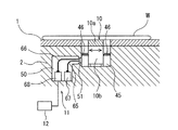
図24は、振動測定部11として光学式センサを用いた例を示す断面図である。この光学式センサは、光を対象物に照射し、対象物から戻ってくる光の強度を測定する装置である。図24は光学式センサの一具体例を示しており、図12に示す振動測定部11としての変位センサを、光学式センサに代えた例を示す。その他の構成は図12または図14に示す例と同様である。図24に示すように、ターゲット10の一部である台座10bの側方には2つの光ファイバー65,66が配置されており、これら光ファイバー65,66の先端は台座10bの側面を向いている。一方の光ファイバー65は光源67に接続され、他方の光ファイバー66は、光の強さを測定する測定部としての光パワーメータ68に接続されている。
FIG. 24 is a cross-sectional view illustrating an example in which an optical sensor is used as the
光源67としては、発光ダイオード(LED)、ハロゲンランプ、キセノンランプなどを用いることができる。光源67の光は光ファイバー65の先端から台座10b(すなわちターゲット10)の側面に照射される。光は台座10bの側面で反射し、光ファイバー66によって受光される。このように、光ファイバー65および光源67は投光部を構成し、光ファイバー66は受光部を構成する。受光された光は光パワーメータ68に送られ、ここで反射光の強さが測定される。
As the
ウェハWとの接触によりターゲット10が振動すると、光ファイバー65,66の先端とターゲット10との距離が変化する。その結果、反射光の強さが変化する。反射光の強さはターゲット10の振動の大きさに応じて変化するので、反射光の強さはターゲット10の振動の大きさに対応する。したがって、光パワーメータ68は、反射光の強さからターゲット10の振動の振幅および周波数を測定することができる。光パワーメータ68は制御部12に接続されており、光パワーメータ68の測定値は制御部12に送られるようになっている。なお、この例では、光ファイバー65,66、光源67、および光パワーメータ68から振動測定部11が構成される。
When the
図25は、図24の変形例を示す断面図である。より詳しくは、図25は、図19に示す振動測定部11としての変位センサを、光学式センサに代えた例を示している。この例では、光ファイバー65,66は弾性バッグ10cの下方に配置される。その他の構成は、図24に示す例と同様である。光は光ファイバー65から弾性バッグ10cを貫通して接触パッド10aに照射され、接触パッド10aで反射した光は弾性バッグ10cを貫通して光ファイバー66に受光される。この例でも、反射光の強さからターゲット10の振動の大きさを測定することができる。
FIG. 25 is a cross-sectional view showing a modification of FIG. More specifically, FIG. 25 shows an example in which the displacement sensor as the
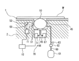
図26は、振動測定部に加え、反射強度測定部を設けた例を示す断面図である。より詳しくは、図26は、図21に示す構成に反射強度測定部70を加えた構成を示している。この反射強度測定部70は、ウェハWの表面に光を照射し、ウェハWから戻ってくる光の強度を測定する装置である。図26に示すように、反射強度測定部70は、弾性バッグ10cの下方に配置された2つの光ファイバー65,66と、これらの光ファイバー65,66にそれぞれ接続された光源67および分光器71とを備えている。光源67としては、発光ダイオード(LED)、ハロゲンランプ、キセノンランプなどを用いることができる。
FIG. 26 is a cross-sectional view showing an example in which a reflection intensity measurement unit is provided in addition to the vibration measurement unit. More specifically, FIG. 26 shows a configuration in which a reflection
この例では、ターゲット10は弾性バッグから構成される。すなわち、この例では接触パッドは弾性バッグに取り付けられていなく、弾性バッグの最上部がウェハWに直接接触するようになっている。この弾性バッグは、光を透過させる透明な材料から構成されている。なお、光を透過させる透明な接触パッドを弾性バッグの最上部に取り付けてもよい。弾性バッグ(ターゲット)10には、図21に示す例と同様に、流体供給源61が流体供給路60を介して連結され、圧力調整機構62および圧力センサ63が流体供給路60に設けられている。
In this example, the
ターゲットである弾性バッグ10には、光を透過させる透明な流体が封入されている。光源67の光は光ファイバー65の先端から弾性バッグ10を貫通してウェハWの下面(被研磨面)に照射される。光はウェハWの下面で反射し、光ファイバー66によって受光される。このように、光ファイバー65および光源67は投光部を構成し、光ファイバー66は受光部を構成する。
A transparent fluid that transmits light is sealed in the
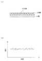
光ファイバー66で受光された光は分光器71に送られる。分光器71は、光を波長に従って分解してスペクトルを生成する。分光器71で得られるスペクトルは、波長ごとの反射強度(反射光の強さ)を示す情報を含んでおり、波長ごとの反射強度が分光器71によって測定される。各波長での反射強度は、ウェハWの膜の厚さに応じて周期的に変化する。図27は、研磨時間に従って変化する反射強度を示すグラフである。図27の横軸は研磨時間(膜厚と考えてもよい)、縦軸は反射強度を示す。図27に示すように、膜厚が減少するにしたがって、反射強度はサインカーブを描いて変化する。これは、膜の表面で反射した光と、その膜を透過して下地層の表面で反射した光とが干渉するためである。
The light received by the
分光器71は制御部12に接続されており、制御部12によって、所定の波長での反射強度、すなわち膜厚が監視されるようになっている。研磨初期では、図27に示すように、研磨の不安定さやノイズ等により反射強度の波形が安定しない場合がある。このため、反射強度のモニター開始を意図的に遅らせ、ある程度研磨が進行した後に反射強度のモニターが開始される。
The spectroscope 71 is connected to the
制御部12は、反射強度を監視することにより、ウェハWの膜が所定の厚さにまで除去されたか否かを判定する。すなわち、制御部12は、モニター開始後に現われる極大値(または極小値)の数をカウントして、予め定められた個数の極大値(または極小値)が現われた時点を検出する。この検出すべき点は、ウェハWの膜が所定の厚さにまで除去された点(以下、目標研磨点という)であり、予め制御部12に設定されている。例えば、図27では、4番目の極大値が目標研磨点として予め設定されている。したがって、モニター開始後の極大値のカウントが4になったときに、制御部12は目標研磨点に達したと判断する。この場合、目標研磨点が表れた時点に所定の時間を加算した時点を研磨終点に設定してもよい。
The
なお、反射強度に代えて、異なる波長での反射強度同士を割り算した値である特性値を用いてもよい。この特定値は、反射強度からノイズ成分などを取り除いた値と考えることができる。この特性値も、反射強度と同様に、膜厚の変化に従って周期的に変化する。特性値を用いる場合は、制御部12は、予め選択された2つの波長λ1,λ2における反射強度ρλ1(t),ρλ2(t)を用いて、特性値X(t)を次の式から求める。
X(t)=ρλ1(t)/(ρλ1(t)+ρλ2(t))
ここで、ρは反射強度、tは研磨時間を表す。
Instead of the reflection intensity, a characteristic value that is a value obtained by dividing the reflection intensities at different wavelengths may be used. This specific value can be considered as a value obtained by removing a noise component from the reflection intensity. Similarly to the reflection intensity, this characteristic value also changes periodically according to the change in the film thickness. When the characteristic value is used, the
X (t) = ρ λ1 (t) / (ρ λ1 (t) + ρ λ2 (t))
Here, ρ represents the reflection intensity, and t represents the polishing time.
上述したスペクトルは、波長ごとの反射光の強度の分布を示すグラフとして表わすことができる。このスペクトルは、ウェハWの膜厚に応じて変化する。したがって、スペクトルと膜厚との関係を示すデータと、研磨中に取得されたスペクトルとから、膜厚を研磨中に求めることができる。具体的には、次のような方法で膜厚を求めることができる。まず、膜の厚さごとのスペクトルをシミュレーション計算によりデータとして取得する。分光器71で得られたスペクトルの波形は、制御部12により、カーブフィッティングなどの手法を用いて、データ中のスペクトルと比較される。そして、分光器で得られたスペクトルに最も近いスペクトルがデータの中から選択され、その選択されたスペクトルに対応する膜厚が研磨中の膜厚と判断される。この方法によれば、制御部12は、膜厚が減少して所定のしきい値に達したときに、目標研磨点または研磨終点に達したと判断することができる。
The spectrum described above can be represented as a graph showing the distribution of the intensity of reflected light for each wavelength. This spectrum changes according to the film thickness of the wafer W. Therefore, the film thickness can be obtained during polishing from the data indicating the relationship between the spectrum and the film thickness and the spectrum acquired during polishing. Specifically, the film thickness can be obtained by the following method. First, a spectrum for each film thickness is acquired as data by simulation calculation. The spectrum waveform obtained by the spectroscope 71 is compared with the spectrum in the data by the
光ファイバー65からの光が照射されるウェハWの部位は、弾性バッグ(ターゲット)10に接触する部位である。つまり、反射光の強度が測定されるウェハWの箇所と、振動および周波数の少なくとも一方が測定されるウェハWの箇所は同一である。したがって、制御部12は、振動測定部11および反射強度測定部70から送られてくる測定値に基づき、ウェハWの同じ領域における研磨状態を監視することができる。この場合、制御部12は、振動測定部11から送られてくる振幅および周波数の少なくとも一方と、反射強度測定部70から送られてくる反射強度とを、同時または交互に監視することができる。例えば、制御部12は、研磨初期における膜の表面の凹凸の除去(図7(a)参照)を振動測定部11からの測定値に基づいて判断し、次いで、研磨終点における膜の除去(図9(a)参照)を反射強度測定部70からの測定値に基づいて判断することができる。または、研磨初期における膜の表面の凹凸の除去を反射強度測定部70からの測定値に基づいて判断し、次いで、研磨終点における膜の除去を振動測定部11からの測定値に基づいて判断してもよい。このように、制御部12は、振幅および周波数の少なくとも一方と反射強度とを選択的に監視することができる。
The part of the wafer W irradiated with light from the
多層構造を有する基板の処理においては、研磨終点検知、膜厚測定、膜の表面の平坦化などの処理の目的に適した研磨監視方法を用いることが有効である。また、膜の性質に適した研磨監視方法を採用することも有効である。例えば、凹凸の大きい表面を平坦にするときは振動測定部11を用いて摩擦の変化を監視し、研磨の最終段階において研磨終点検知が必要なときには反射強度測定部70を用いて反射強度(すなわち膜厚の変化)を監視することが好ましい。さらに、制御部12は、振動測定部11および反射強度測定部70の両方を用いて摩擦の変化と反射強度とを同時に監視してもよい。
In processing a substrate having a multilayer structure, it is effective to use a polishing monitoring method suitable for processing purposes such as polishing end point detection, film thickness measurement, and film surface flattening. It is also effective to employ a polishing monitoring method suitable for the properties of the film. For example, when flattening a rough surface, the
図28は、振動測定部に加えて、基板の被研磨面の画像を取得するカメラを備えた例を示す断面図である。この例では、図26に示す反射強度測定部70に代えて、ウェハWの被研磨面の画像を取得するカメラ(画像取得手段)72が配置されている。その他の構成は、図26に示す例と同一であるので、その重複する説明を省略する。カメラ72は、ターゲットである弾性バッグ10の下方に配置されている。カメラ72としては、CCDなどのイメージセンサを用いたデジタルスチールカメラが好ましく用いられる。カメラ72は、研磨テーブル2に形成された孔の内部に配置されており、孔の上端には研磨液などの液体の侵入を防ぐ透明窓51が設けられている。弾性バッグ10は、光透過性を有する材料から構成されており、弾性バッグ10には、光を透過させる透明な流体が封入されている。
FIG. 28 is a cross-sectional view illustrating an example provided with a camera that acquires an image of a surface to be polished of a substrate in addition to the vibration measurement unit. In this example, a camera (image acquisition unit) 72 that acquires an image of the surface to be polished of the wafer W is disposed instead of the reflection
ウェハWの研磨中は、ウェハWの表面と弾性バッグ10とが接触し、これにより弾性バッグ10が振動する。振動測定部11は、上述の例と同様に、弾性バッグ10の振動の振幅および周波数の少なくとも一方を測定し、その測定値を制御部12に送信する。一方、カメラ72は、ウェハWの研磨中、ウェハWの表面の画像を撮像する。具体的には、カメラ72は、弾性バッグ10と接触しているウェハWの表面の領域の画像を、弾性バッグ10を通じて取得する。なお、図示しないが、撮影用の光源が弾性バッグ(ターゲット)10に近接して設けられている。この光源としては、連続光を発するライト、またはフラッシュなどが用いられる。
During the polishing of the wafer W, the surface of the wafer W and the
カメラ72が取得した画像は画像解析部73に送られる。画像解析部73は、ウェハWの表面の画像から、ウェハWの構造を解析する。具体的には、画像解析部73は、画像に現われるウェハWの表面の模様および色から、スクライブラインの位置や、スクライブライン上のテストエレメントを測定したり、セルの位置や面積を測定する。このように、ウェハWの構造の解析と振動測定部11による測定結果とを関連づけることで、ウェハWの研磨状態をより正確に判断することができる。上はまた、画像解析部73は、取得した画像から膜厚を測定したり、構造上の欠陥を検知してもよい。画像解析部73の解析結果は、制御部12に送られ、研磨処理の制御に使用される。
The image acquired by the
図29は、振動測定部として、カメラおよび画像解析部を用いた例を示す断面図である。その他の構成は、図19に示す例と同一であるので、その重複する説明を省略する。この例の振動測定部11は、ターゲット10の画像を取得するカメラ(画像取得手段)72を備えている。このカメラ72は、ターゲット10の下方に配置されている。カメラ72としては、CCDなどのイメージセンサを用いたデジタルスチールカメラが好ましく用いられる。この例では、図19に示す例と同様に、ターゲット10は、弾性バッグ10cと、弾性バッグ10cの頂部に取り付けられた接触パッド10aとを有している。カメラ72は、研磨テーブル2に形成された孔の内部に配置されており、孔の上端には研磨液などの液体の侵入を防ぐ透明窓51が設けられている。弾性バッグ10cは、光透過性を有する材料から構成されており、弾性バッグ10cには、光を透過させる透明な流体が封入されている。
FIG. 29 is a cross-sectional view illustrating an example in which a camera and an image analysis unit are used as the vibration measurement unit. Other configurations are the same as the example shown in FIG. The
カメラ72はターゲット10に対向して配置されており、研磨中にターゲット10の画像を取得するように動作する。なお、図示しないが、撮影用の光源がターゲット10に近接して設けられている。この光源としては、連続光を発するライト、またはフラッシュなどが用いられる。ターゲット10には模様が予め付されており、カメラ72はこのターゲット10上の模様の画像を取得する。この例では、カメラ72は、接触パッド10aの裏面の画像を取得するように配置されている。接触パッド10aの裏面には、同心円、格子状の線などの模様が付されている。カメラ72は、研磨中に、接触パッド10aの裏面(模様を含む)の画像を、弾性バッグ10cを通じて取得する。この場合、接触パッド10aを透明な材料で構成し、その裏面に付された模様を観察すると同時に、ウェハWの表面の画像を制御部12により観察してもよい。
The
カメラ72が取得した画像は画像解析部74に送られる。画像解析部74は、ターゲット10の画像から、ターゲット10の振動の振幅および周波数の少なくとも一方を解析する。取得された画像には、上述したように、ターゲット10に付された模様が現われているので、画像解析部74は、この模様の変位から、ターゲット10の振動の振幅および周波数の少なくとも一方を解析することができる。ターゲット10の振動の方向および大きさの解析が容易となるように、模様の変位や変位の方向を画像解析部74が認識しやすいような模様であることが好ましい。画像解析部74の解析結果(すなわち、ターゲット10の振動の振幅および周波数の少なくとも一方)は、制御部12に送信され、制御部12によって研磨処理の制御に使用される。
The image acquired by the
なお、図28に示す例と同様に、接触パッドを有しない弾性バッグをターゲット10として用いてもよい。この場合は、ウェハWの表面に接触する弾性バッグの裏面に模様が付され、カメラ72は、弾性バッグを介して模様の画像を取得する。また、図29に示す実施形態は、ターゲットとして弾性バッグを用いた例に限らず、例えば図12に示すように、ウェハWに接触する接触パッド10aと、接触パッド10aを保持する台座10bとを備えたターゲットを使用した例にも適用することができる。この場合は、台座10bの下面に模様を付し、カメラ72によって台座10bの下面(模様を含む)の画像を取得するようにしてもよい。
As in the example shown in FIG. 28, an elastic bag that does not have a contact pad may be used as the
上述した構成例では、ターゲット10は弾性的に研磨テーブル2に連結されているため、回転する研磨テーブル2自体の振動がターゲット10に伝わる場合がある。このような研磨テーブル2の振動はノイズとして振動測定部11の測定値に重畳されてしまう。そこで、振動測定部11とは別に、リファレンスセンサ(リファレンス測定部)を研磨テーブル2に設け、リファレンスセンサの測定値を利用して、振動測定部11の測定値からノイズを除去することが好ましい。
In the configuration example described above, since the
図30は、研磨テーブル2にリファレンスセンサを設けた例を示す断面図である。リファレンスセンサ75は、研磨テーブル2の内部または研磨テーブル2の表面上に設置される。振動測定部11がターゲット10の振動を測定すると同時に、リファレンスセンサ75は、研磨テーブル2の所定の部位の振動の大きさを測定する。リファレンスセンサ75によって測定される対象は、ターゲット10とウェハWとの接触に起因する振動以外のあらゆる振動、つまりノイズである。このノイズは、例えば研磨テーブル2、トップリング3のそれぞれ固有の偏心やがたつきなどに起因する機械的振動、駆動モータの振動などである。
FIG. 30 is a cross-sectional view showing an example in which a reference sensor is provided on the polishing table 2. The
リファレンスセンサ75の測定値は制御部12に送られる。振動測定部11の測定値は、リファレンスセンサ75の測定値で除算され、これにより振動測定部11の測定値に含まれるノイズが取り除かれる。図30に示すように、リファレンスセンサ75が測定する研磨テーブル2の部位は、ターゲット10の近くであることが好ましい。これはノイズを正確にキャンセルするために、振動測定部11のノイズとなるべく同種のノイズをリファレンスセンサ75で測定するためである。振動測定部11とリファレンスセンサ75とは、同一のタイプのセンサが用いられる。本例においては、リファレンスセンサは1つであるが、複数のリファレンスセンサを設置してもよい。この場合、複数のリファレンスセンサの信号強度比を変えてから振動測定部11の測定値を除算すると効果的な場合がある。例えば、同じタイプのリファレンスセンサを使う場合、信号感度がセンサごとに異なることがある。このような場合は、それぞれのリファレンスセンサの信号強度を調整して一致させる。一方、異なるレファレンスセンサを組み合わせて使う場合は、必ずしも信号感度が一致するとは限らないので、信号強度を調整して一致させる。
The measurement value of the
上述した実施形態では、研磨中にターゲットの振動の大きさ(および反射光の強度)が測定される。しかしながら、より高い測定精度が必要な場合、または測定部を研磨テーブルに内蔵することが困難な場合は、研磨テーブル外に専用の測定部を設け、ここで測定を行ってもよい。この場合、研磨開始時、研磨中断時、または研磨終了後に測定を行うことができる。また、専用の測定部に代えて、ウェハ(基板)を洗浄する洗浄ユニットや、ウェハを搬送する搬送機構などの基板処理装置を構成する機構に測定部を設けてもよい。例えば、搬送機構に設けられた測定部により、ウェハの搬送中に測定を行ってもよい。 In the embodiment described above, the magnitude of the target vibration (and the intensity of the reflected light) is measured during polishing. However, when higher measurement accuracy is required, or when it is difficult to incorporate the measurement unit in the polishing table, a dedicated measurement unit may be provided outside the polishing table and measurement may be performed here. In this case, the measurement can be performed at the start of polishing, when polishing is interrupted, or after the polishing is completed. Further, instead of the dedicated measurement unit, the measurement unit may be provided in a mechanism that constitutes a substrate processing apparatus such as a cleaning unit that cleans the wafer (substrate) or a transport mechanism that transports the wafer. For example, the measurement may be performed while the wafer is being transferred by a measurement unit provided in the transfer mechanism.
上述した実施形態は、本発明が属する技術分野における通常の知識を有する者が本発明を実施できることを目的として記載されたものである。上記実施形態の種々の変形例は、当業者であれば当然になしうることであり、本発明の技術的思想は他の実施形態にも適用しうることである。したがって、本発明は、記載された実施形態に限定されることはなく、特許請求の範囲によって定義される技術的思想に従った最も広い範囲とすべきである。 The embodiment described above is described for the purpose of enabling the person having ordinary knowledge in the technical field to which the present invention belongs to implement the present invention. Various modifications of the above embodiment can be naturally made by those skilled in the art, and the technical idea of the present invention can be applied to other embodiments. Therefore, the present invention should not be limited to the described embodiments, but should be the widest scope according to the technical idea defined by the claims.
1 研磨パッド
2 研磨テーブル
3 トップリング
4 研磨液供給ノズル
6 トップリングシャフト
10 ターゲット
11 振動測定部
12 制御部
15 変位変換部材
20 自由継手
21 トップリング本体
22 リテーナリング
26 弾性パッド
27 チャッキングプレート
31〜35 流体路
40 圧力調整部
45 凹部
46 ばね
50 部屋
52 ミラー
54 液体供給路
55 液体排出路
57 切れ込み線
58 閉塞プレート
60 流体供給路
61 流体供給源
62 圧力調整機構
63 圧力センサ
65,66 光ファイバー
67 光源
68 光パワーメータ
70 反射強度測定部
71 分光器
72 カメラ
73,74 画像解析部
75 リファレンスセンサ
DESCRIPTION OF
Claims (31)
基板を前記研磨面に押圧する基板保持部とを有し、前記研磨テーブルと前記基板保持部の相対移動により基板の表面を研磨する研磨装置であって、
前記基板の表面に接触するターゲットと、
前記ターゲットの振動の振幅および周波数の少なくとも一方を測定する振動測定部と、
前記振動測定部によって測定された前記振幅および周波数の少なくとも一方に基づいて研磨処理を制御する制御部とを備えたことを特徴とする研磨装置。 A polishing table to which a polishing pad having a polishing surface is attached;
A polishing apparatus that has a substrate holding part that presses the substrate against the polishing surface, and polishes the surface of the substrate by relative movement of the polishing table and the substrate holding part,
A target in contact with the surface of the substrate;
A vibration measuring unit that measures at least one of amplitude and frequency of vibration of the target;
A polishing apparatus comprising: a control unit that controls polishing processing based on at least one of the amplitude and frequency measured by the vibration measuring unit.
前記制御部は、前記振動測定部によって測定された前記振幅および周波数の少なくとも一方に基づいて、前記複数の押圧機構の押圧力を制御することを特徴とする請求項1に記載の研磨装置。 The substrate holding part has a plurality of pressing mechanisms that independently press a plurality of regions of the substrate,
The polishing apparatus according to claim 1, wherein the control unit controls the pressing force of the plurality of pressing mechanisms based on at least one of the amplitude and frequency measured by the vibration measuring unit.
前記ターゲットは、前記液体室内に配置されていることを特徴とする請求項1に記載の研磨装置。 The polishing table is provided with a liquid chamber that opens on its upper surface,
The polishing apparatus according to claim 1, wherein the target is disposed in the liquid chamber.
前記接触パッドは、前記弾性バッグに取り付けられており、
前記振動測定部は、前記接触パッドの振動の振幅および周波数の少なくとも一方を測定することを特徴とする請求項5に記載の研磨装置。 The target further includes a contact pad that contacts the surface of the substrate;
The contact pad is attached to the elastic bag;
The polishing apparatus according to claim 5, wherein the vibration measuring unit measures at least one of an amplitude and a frequency of vibration of the contact pad.
前記弾性バッグを介して前記基板の表面の画像を取得する画像取得手段をさらに備えていることを特徴とする請求項5に記載の研磨装置。 The elastic bag is made of a light transmissive material,
The polishing apparatus according to claim 5, further comprising an image acquisition unit that acquires an image of the surface of the substrate through the elastic bag.
前記ターゲットの画像を取得する画像取得手段と、
前記画像取得手段によって取得された画像から前記ターゲットの振動の振幅および周波数の少なくとも一方を解析する画像解析部とを備えていることを特徴とする請求項1に記載の研磨装置。 The vibration measuring unit is
Image acquisition means for acquiring an image of the target;
The polishing apparatus according to claim 1, further comprising: an image analysis unit that analyzes at least one of an amplitude and a frequency of the vibration of the target from an image acquired by the image acquisition unit.
前記ターゲットに光を照射する投光部と、
前記ターゲットで反射した光を受光する受光部と、
前記受光部によって受光された光の強さを測定する測定部とを有することを特徴とする請求項1に記載の研磨装置。 The vibration measuring unit is
A light projecting unit for irradiating the target with light;
A light receiving unit for receiving light reflected by the target;
The polishing apparatus according to claim 1, further comprising a measuring unit that measures the intensity of light received by the light receiving unit.
前記振動測定部は前記研磨テーブルに設けられ、
前記制御部は、前記振動測定部の測定値から前記リファレンス測定部の測定値を除算することを特徴とする請求項1に記載の研磨装置。 A reference measurement unit for measuring at least one of amplitude and frequency of vibration of the polishing table;
The vibration measuring unit is provided on the polishing table,
The polishing apparatus according to claim 1, wherein the control unit divides the measurement value of the reference measurement unit from the measurement value of the vibration measurement unit.
研磨テーブルに取り付けられた研磨パッドの研磨面に基板を押圧し、
前記基板保持部と前記研磨テーブルとを相対移動させて前記基板の表面を研磨し、
研磨中に、前記基板の表面に接触するターゲットの振動の振幅および周波数の少なくとも一方を測定し、
測定された前記振幅および周波数の少なくとも一方に基づいて研磨処理を制御することを特徴とする研磨方法。 Hold the substrate by the substrate holder,
Press the substrate against the polishing surface of the polishing pad attached to the polishing table,
Polishing the surface of the substrate by relatively moving the substrate holding unit and the polishing table;
During polishing, measure at least one of amplitude and frequency of vibration of the target that contacts the surface of the substrate;
A polishing method, wherein polishing processing is controlled based on at least one of the measured amplitude and frequency.
前記画像から前記基板の表面の構造を解析することを特徴とする請求項23に記載の研磨方法。 During polishing, acquire an image of the surface of the substrate,
The polishing method according to claim 23, wherein the structure of the surface of the substrate is analyzed from the image.
前記画像から前記ターゲットの振動の振幅および周波数の少なくとも一方を解析することを特徴とする請求項23に記載の研磨方法。 During polishing, acquire an image of the target,
The polishing method according to claim 23, wherein at least one of an amplitude and a frequency of vibration of the target is analyzed from the image.
Priority Applications (1)
| Application Number | Priority Date | Filing Date | Title |
|---|---|---|---|
| JP2008234991A JP5301931B2 (en) | 2008-09-12 | 2008-09-12 | Polishing method and polishing apparatus |
Applications Claiming Priority (1)
| Application Number | Priority Date | Filing Date | Title |
|---|---|---|---|
| JP2008234991A JP5301931B2 (en) | 2008-09-12 | 2008-09-12 | Polishing method and polishing apparatus |
Publications (3)
| Publication Number | Publication Date |
|---|---|
| JP2010064220A true JP2010064220A (en) | 2010-03-25 |
| JP2010064220A5 JP2010064220A5 (en) | 2011-10-13 |
| JP5301931B2 JP5301931B2 (en) | 2013-09-25 |
Family
ID=42190253
Family Applications (1)
| Application Number | Title | Priority Date | Filing Date |
|---|---|---|---|
| JP2008234991A Expired - Fee Related JP5301931B2 (en) | 2008-09-12 | 2008-09-12 | Polishing method and polishing apparatus |
Country Status (1)
| Country | Link |
|---|---|
| JP (1) | JP5301931B2 (en) |
Cited By (13)
| Publication number | Priority date | Publication date | Assignee | Title |
|---|---|---|---|---|
| KR20120010180A (en) * | 2010-07-23 | 2012-02-02 | 가부시키가이샤 에바라 세이사꾸쇼 | Method of monitoring progress of substrate polishing and polishing apparatus |
| CN106112810A (en) * | 2016-08-08 | 2016-11-16 | 泉州装备制造研究所 | Stone grinder system failure Intelligent Measurement and analysis method and apparatus |
| US9502318B2 (en) | 2014-06-17 | 2016-11-22 | Kabushiki Kaisha Toshiba | Polish apparatus, polish method, and method of manufacturing semiconductor device |
| US9902038B2 (en) | 2015-02-05 | 2018-02-27 | Toshiba Memory Corporation | Polishing apparatus, polishing method, and semiconductor manufacturing method |
| WO2018052816A1 (en) * | 2016-09-15 | 2018-03-22 | Applied Materials, Inc. | Chemical mechanical polishing smart ring |
| JP2019081243A (en) * | 2017-10-31 | 2019-05-30 | 株式会社荏原製作所 | Polishing device and polishing method |
| WO2020046502A1 (en) * | 2018-08-31 | 2020-03-05 | Applied Materials, Inc. | Polishing system with capacitive shear sensor |
| CN111002214A (en) * | 2019-12-25 | 2020-04-14 | 唐山万士和电子有限公司 | Piezoelectric quartz wafer convex surface grinding frequency real-time monitoring device |
| CN111263682A (en) * | 2018-03-13 | 2020-06-09 | 应用材料公司 | Monitoring of vibrations during chemical mechanical polishing |
| JP2020185659A (en) * | 2019-05-17 | 2020-11-19 | Agc株式会社 | Abnormality detection device and abnormality detection method |
| CN112384330A (en) * | 2019-01-23 | 2021-02-19 | 应用材料公司 | Polishing pads formed using additive manufacturing processes and related methods |
| US11688653B2 (en) | 2020-03-06 | 2023-06-27 | Kioxia Corporation | Semiconductor manufacturing apparatus and method of manufacturing semiconductor device |
| JP7468856B2 (en) | 2019-12-03 | 2024-04-16 | 株式会社荏原製作所 | Polishing apparatus and polishing method |
Families Citing this family (1)
| Publication number | Priority date | Publication date | Assignee | Title |
|---|---|---|---|---|
| JP2021144972A (en) | 2020-03-10 | 2021-09-24 | キオクシア株式会社 | Apparatus for manufacturing semiconductor |
Citations (6)
| Publication number | Priority date | Publication date | Assignee | Title |
|---|---|---|---|---|
| JP2003236749A (en) * | 1995-04-26 | 2003-08-26 | Fujitsu Ltd | Polishing device and polishing method |
| JP2006187837A (en) * | 2005-01-06 | 2006-07-20 | Toyo Tire & Rubber Co Ltd | Polishing pad |
| JP2007027781A (en) * | 1995-03-28 | 2007-02-01 | Applied Materials Inc | Polishing pad |
| JP2007044814A (en) * | 2005-08-10 | 2007-02-22 | Nitta Haas Inc | Polishing pad |
| JP2007059597A (en) * | 2005-08-24 | 2007-03-08 | Fuji Electric Holdings Co Ltd | Film thickness evaluation method, polish end point detecting method, and device manufacturing equipment |
| JP2008068388A (en) * | 2006-09-15 | 2008-03-27 | Tokyo Seimitsu Co Ltd | Electrostatically coupled type sensor, end point detection method using the same, and device thereof |
-
2008
- 2008-09-12 JP JP2008234991A patent/JP5301931B2/en not_active Expired - Fee Related
Patent Citations (6)
| Publication number | Priority date | Publication date | Assignee | Title |
|---|---|---|---|---|
| JP2007027781A (en) * | 1995-03-28 | 2007-02-01 | Applied Materials Inc | Polishing pad |
| JP2003236749A (en) * | 1995-04-26 | 2003-08-26 | Fujitsu Ltd | Polishing device and polishing method |
| JP2006187837A (en) * | 2005-01-06 | 2006-07-20 | Toyo Tire & Rubber Co Ltd | Polishing pad |
| JP2007044814A (en) * | 2005-08-10 | 2007-02-22 | Nitta Haas Inc | Polishing pad |
| JP2007059597A (en) * | 2005-08-24 | 2007-03-08 | Fuji Electric Holdings Co Ltd | Film thickness evaluation method, polish end point detecting method, and device manufacturing equipment |
| JP2008068388A (en) * | 2006-09-15 | 2008-03-27 | Tokyo Seimitsu Co Ltd | Electrostatically coupled type sensor, end point detection method using the same, and device thereof |
Cited By (23)
| Publication number | Priority date | Publication date | Assignee | Title |
|---|---|---|---|---|
| KR20120010180A (en) * | 2010-07-23 | 2012-02-02 | 가부시키가이샤 에바라 세이사꾸쇼 | Method of monitoring progress of substrate polishing and polishing apparatus |
| JP2012028554A (en) * | 2010-07-23 | 2012-02-09 | Ebara Corp | Method of monitoring substrate polishing progress, and polishing device |
| KR101669554B1 (en) | 2010-07-23 | 2016-10-26 | 가부시키가이샤 에바라 세이사꾸쇼 | Method of monitoring progress of substrate polishing and polishing apparatus |
| US9502318B2 (en) | 2014-06-17 | 2016-11-22 | Kabushiki Kaisha Toshiba | Polish apparatus, polish method, and method of manufacturing semiconductor device |
| US9902038B2 (en) | 2015-02-05 | 2018-02-27 | Toshiba Memory Corporation | Polishing apparatus, polishing method, and semiconductor manufacturing method |
| CN106112810A (en) * | 2016-08-08 | 2016-11-16 | 泉州装备制造研究所 | Stone grinder system failure Intelligent Measurement and analysis method and apparatus |
| US10513008B2 (en) | 2016-09-15 | 2019-12-24 | Applied Materials, Inc. | Chemical mechanical polishing smart ring |
| WO2018052816A1 (en) * | 2016-09-15 | 2018-03-22 | Applied Materials, Inc. | Chemical mechanical polishing smart ring |
| JP2019081243A (en) * | 2017-10-31 | 2019-05-30 | 株式会社荏原製作所 | Polishing device and polishing method |
| JP7403213B2 (en) | 2017-10-31 | 2023-12-22 | 株式会社荏原製作所 | Polishing device and polishing method |
| CN111263682A (en) * | 2018-03-13 | 2020-06-09 | 应用材料公司 | Monitoring of vibrations during chemical mechanical polishing |
| JP7354131B2 (en) | 2018-03-13 | 2023-10-02 | アプライド マテリアルズ インコーポレイテッド | Vibration monitoring during chemical mechanical polishing |
| US11701749B2 (en) | 2018-03-13 | 2023-07-18 | Applied Materials, Inc. | Monitoring of vibrations during chemical mechanical polishing |
| JP2021517073A (en) * | 2018-03-13 | 2021-07-15 | アプライド マテリアルズ インコーポレイテッドApplied Materials,Incorporated | Vibration monitoring during chemical polishing |
| US11660722B2 (en) | 2018-08-31 | 2023-05-30 | Applied Materials, Inc. | Polishing system with capacitive shear sensor |
| WO2020046502A1 (en) * | 2018-08-31 | 2020-03-05 | Applied Materials, Inc. | Polishing system with capacitive shear sensor |
| CN112384330B (en) * | 2019-01-23 | 2022-12-30 | 应用材料公司 | Polishing pads formed using additive manufacturing processes and related methods |
| CN112384330A (en) * | 2019-01-23 | 2021-02-19 | 应用材料公司 | Polishing pads formed using additive manufacturing processes and related methods |
| JP7306054B2 (en) | 2019-05-17 | 2023-07-11 | Agc株式会社 | Anomaly detection device and anomaly detection method |
| JP2020185659A (en) * | 2019-05-17 | 2020-11-19 | Agc株式会社 | Abnormality detection device and abnormality detection method |
| JP7468856B2 (en) | 2019-12-03 | 2024-04-16 | 株式会社荏原製作所 | Polishing apparatus and polishing method |
| CN111002214A (en) * | 2019-12-25 | 2020-04-14 | 唐山万士和电子有限公司 | Piezoelectric quartz wafer convex surface grinding frequency real-time monitoring device |
| US11688653B2 (en) | 2020-03-06 | 2023-06-27 | Kioxia Corporation | Semiconductor manufacturing apparatus and method of manufacturing semiconductor device |
Also Published As
| Publication number | Publication date |
|---|---|
| JP5301931B2 (en) | 2013-09-25 |
Similar Documents
| Publication | Publication Date | Title |
|---|---|---|
| JP5301931B2 (en) | Polishing method and polishing apparatus | |
| JP6208299B2 (en) | Polishing device | |
| KR101669554B1 (en) | Method of monitoring progress of substrate polishing and polishing apparatus | |
| TWI569318B (en) | Grinding apparatus and grinding method | |
| TWI812630B (en) | Substrate polishing apparatus and method | |
| TWI788383B (en) | Polishing apparatus and polishing method | |
| JP6469785B2 (en) | Polishing pad | |
| JP6275421B2 (en) | Polishing method and polishing apparatus |
Legal Events
| Date | Code | Title | Description |
|---|---|---|---|
| A521 | Written amendment |
Free format text: JAPANESE INTERMEDIATE CODE: A523 Effective date: 20110826 |
|
| A621 | Written request for application examination |
Free format text: JAPANESE INTERMEDIATE CODE: A621 Effective date: 20110826 |
|
| A131 | Notification of reasons for refusal |
Free format text: JAPANESE INTERMEDIATE CODE: A131 Effective date: 20130108 |
|
| A521 | Written amendment |
Free format text: JAPANESE INTERMEDIATE CODE: A523 Effective date: 20130308 |
|
| TRDD | Decision of grant or rejection written | ||
| A01 | Written decision to grant a patent or to grant a registration (utility model) |
Free format text: JAPANESE INTERMEDIATE CODE: A01 Effective date: 20130604 |
|
| A61 | First payment of annual fees (during grant procedure) |
Free format text: JAPANESE INTERMEDIATE CODE: A61 Effective date: 20130620 |
|
| R150 | Certificate of patent or registration of utility model |
Free format text: JAPANESE INTERMEDIATE CODE: R150 |
|
| R250 | Receipt of annual fees |
Free format text: JAPANESE INTERMEDIATE CODE: R250 |
|
| LAPS | Cancellation because of no payment of annual fees |