JP2010063017A - Rfid tag, rfid tag set and rfid system - Google Patents
Rfid tag, rfid tag set and rfid system Download PDFInfo
- Publication number
- JP2010063017A JP2010063017A JP2008228819A JP2008228819A JP2010063017A JP 2010063017 A JP2010063017 A JP 2010063017A JP 2008228819 A JP2008228819 A JP 2008228819A JP 2008228819 A JP2008228819 A JP 2008228819A JP 2010063017 A JP2010063017 A JP 2010063017A
- Authority
- JP
- Japan
- Prior art keywords
- rfid tag
- antenna
- rfid
- conductor plate
- conductor portion
- Prior art date
- Legal status (The legal status is an assumption and is not a legal conclusion. Google has not performed a legal analysis and makes no representation as to the accuracy of the status listed.)
- Granted
Links
- 239000004020 conductor Substances 0.000 claims abstract description 101
- 239000000758 substrate Substances 0.000 claims abstract description 28
- 238000005452 bending Methods 0.000 claims description 4
- 229910052751 metal Inorganic materials 0.000 abstract description 24
- 239000002184 metal Substances 0.000 abstract description 24
- 238000004891 communication Methods 0.000 abstract description 15
- 230000006866 deterioration Effects 0.000 abstract 1
- 238000010586 diagram Methods 0.000 description 6
- -1 polyethylene Polymers 0.000 description 6
- 229920000139 polyethylene terephthalate Polymers 0.000 description 4
- 239000005020 polyethylene terephthalate Substances 0.000 description 4
- 238000004088 simulation Methods 0.000 description 4
- 238000004519 manufacturing process Methods 0.000 description 3
- 229910001220 stainless steel Inorganic materials 0.000 description 3
- 239000010935 stainless steel Substances 0.000 description 3
- RYGMFSIKBFXOCR-UHFFFAOYSA-N Copper Chemical compound [Cu] RYGMFSIKBFXOCR-UHFFFAOYSA-N 0.000 description 2
- 239000004698 Polyethylene Substances 0.000 description 2
- 239000004642 Polyimide Substances 0.000 description 2
- 239000004743 Polypropylene Substances 0.000 description 2
- 229910000831 Steel Inorganic materials 0.000 description 2
- 230000004913 activation Effects 0.000 description 2
- 229910052782 aluminium Inorganic materials 0.000 description 2
- XAGFODPZIPBFFR-UHFFFAOYSA-N aluminium Chemical compound [Al] XAGFODPZIPBFFR-UHFFFAOYSA-N 0.000 description 2
- 229910052802 copper Inorganic materials 0.000 description 2
- 239000010949 copper Substances 0.000 description 2
- 230000000694 effects Effects 0.000 description 2
- 230000005684 electric field Effects 0.000 description 2
- 239000000463 material Substances 0.000 description 2
- 238000000034 method Methods 0.000 description 2
- 230000004048 modification Effects 0.000 description 2
- 238000012986 modification Methods 0.000 description 2
- 229920000573 polyethylene Polymers 0.000 description 2
- 229920001721 polyimide Polymers 0.000 description 2
- 229920001155 polypropylene Polymers 0.000 description 2
- 230000008569 process Effects 0.000 description 2
- 239000010959 steel Substances 0.000 description 2
- 229920003002 synthetic resin Polymers 0.000 description 2
- 239000000057 synthetic resin Substances 0.000 description 2
- 230000008859 change Effects 0.000 description 1
- 238000009826 distribution Methods 0.000 description 1
- 238000005530 etching Methods 0.000 description 1
- 238000007689 inspection Methods 0.000 description 1
- 230000005404 monopole Effects 0.000 description 1
- 238000004080 punching Methods 0.000 description 1
Images


Classifications
-
- H—ELECTRICITY
- H01—ELECTRIC ELEMENTS
- H01Q—ANTENNAS, i.e. RADIO AERIALS
- H01Q9/00—Electrically-short antennas having dimensions not more than twice the operating wavelength and consisting of conductive active radiating elements
- H01Q9/04—Resonant antennas
- H01Q9/30—Resonant antennas with feed to end of elongated active element, e.g. unipole
- H01Q9/42—Resonant antennas with feed to end of elongated active element, e.g. unipole with folded element, the folded parts being spaced apart a small fraction of the operating wavelength
-
- G—PHYSICS
- G06—COMPUTING; CALCULATING OR COUNTING
- G06K—GRAPHICAL DATA READING; PRESENTATION OF DATA; RECORD CARRIERS; HANDLING RECORD CARRIERS
- G06K19/00—Record carriers for use with machines and with at least a part designed to carry digital markings
- G06K19/06—Record carriers for use with machines and with at least a part designed to carry digital markings characterised by the kind of the digital marking, e.g. shape, nature, code
- G06K19/067—Record carriers with conductive marks, printed circuits or semiconductor circuit elements, e.g. credit or identity cards also with resonating or responding marks without active components
- G06K19/07—Record carriers with conductive marks, printed circuits or semiconductor circuit elements, e.g. credit or identity cards also with resonating or responding marks without active components with integrated circuit chips
- G06K19/077—Constructional details, e.g. mounting of circuits in the carrier
- G06K19/07749—Constructional details, e.g. mounting of circuits in the carrier the record carrier being capable of non-contact communication, e.g. constructional details of the antenna of a non-contact smart card
- G06K19/07771—Constructional details, e.g. mounting of circuits in the carrier the record carrier being capable of non-contact communication, e.g. constructional details of the antenna of a non-contact smart card the record carrier comprising means for minimising adverse effects on the data communication capability of the record carrier, e.g. minimising Eddy currents induced in a proximate metal or otherwise electromagnetically interfering object
-
- H—ELECTRICITY
- H01—ELECTRIC ELEMENTS
- H01Q—ANTENNAS, i.e. RADIO AERIALS
- H01Q1/00—Details of, or arrangements associated with, antennas
- H01Q1/12—Supports; Mounting means
- H01Q1/22—Supports; Mounting means by structural association with other equipment or articles
- H01Q1/2208—Supports; Mounting means by structural association with other equipment or articles associated with components used in interrogation type services, i.e. in systems for information exchange between an interrogator/reader and a tag/transponder, e.g. in Radio Frequency Identification [RFID] systems
-
- H—ELECTRICITY
- H01—ELECTRIC ELEMENTS
- H01Q—ANTENNAS, i.e. RADIO AERIALS
- H01Q1/00—Details of, or arrangements associated with, antennas
- H01Q1/48—Earthing means; Earth screens; Counterpoises
-
- H—ELECTRICITY
- H01—ELECTRIC ELEMENTS
- H01Q—ANTENNAS, i.e. RADIO AERIALS
- H01Q5/00—Arrangements for simultaneous operation of antennas on two or more different wavebands, e.g. dual-band or multi-band arrangements
-
- H—ELECTRICITY
- H01—ELECTRIC ELEMENTS
- H01Q—ANTENNAS, i.e. RADIO AERIALS
- H01Q5/00—Arrangements for simultaneous operation of antennas on two or more different wavebands, e.g. dual-band or multi-band arrangements
- H01Q5/20—Arrangements for simultaneous operation of antennas on two or more different wavebands, e.g. dual-band or multi-band arrangements characterised by the operating wavebands
- H01Q5/25—Ultra-wideband [UWB] systems, e.g. multiple resonance systems; Pulse systems
-
- H—ELECTRICITY
- H01—ELECTRIC ELEMENTS
- H01Q—ANTENNAS, i.e. RADIO AERIALS
- H01Q9/00—Electrically-short antennas having dimensions not more than twice the operating wavelength and consisting of conductive active radiating elements
- H01Q9/04—Resonant antennas
- H01Q9/16—Resonant antennas with feed intermediate between the extremities of the antenna, e.g. centre-fed dipole
Landscapes
- Engineering & Computer Science (AREA)
- Physics & Mathematics (AREA)
- Computer Hardware Design (AREA)
- Microelectronics & Electronic Packaging (AREA)
- General Physics & Mathematics (AREA)
- Theoretical Computer Science (AREA)
- Electromagnetism (AREA)
- Details Of Aerials (AREA)
- Waveguide Aerials (AREA)
- Support Of Aerials (AREA)
- Near-Field Transmission Systems (AREA)
- Variable-Direction Aerials And Aerial Arrays (AREA)
Abstract
Description
本発明は、RFIDタグ、RFIDタグセット及びRFIDシステムに関し、特に、金属物体に付して無線通信するのに好適なRFIDタグ、RFIDタグセット及びRFIDシステムに関する。 The present invention relates to an RFID tag, an RFID tag set, and an RFID system, and more particularly, to an RFID tag, an RFID tag set, and an RFID system suitable for wireless communication with a metal object.
従来、物流管理、商品管理などの効率化を図るべく、RFID(Radio Frequency Identification)システムが利用されている。このRFIDシステムは、ICチップを備えたRFIDタグと該RFIDタグとの間で無線通信を行うリーダあるいはリーダライタとから構成されている。このRFIDタグは、様々なものに取り付けられて運用されるが、取付対象の影響により交信距離に変化が生ずることがある。特に、取付対象が金属面であると著しく交信距離が低下する。 Conventionally, an RFID (Radio Frequency Identification) system has been used in order to improve the efficiency of distribution management, product management, and the like. This RFID system is composed of an RFID tag having an IC chip and a reader or reader / writer that performs wireless communication between the RFID tag. The RFID tag is used by being attached to various things, but there may be a change in the communication distance due to the influence of the attachment target. In particular, when the attachment target is a metal surface, the communication distance is significantly reduced.
また、全ての物品に対してRFIDタグを付して物品管理や商品管理などを行う場合、RFIDタグの形状は、なるべく突起のない形状で、かつ薄型である方が扱いやすい。 In addition, when performing RFID tag management on all articles for article management or merchandise management, it is easier to handle the RFID tag as thin as possible and thin.
従来、上記要請を充足するRFIDタグ、すなわち、金属面に取り付けても交信距離が低下せず、かつ、突起が少なく薄型形状のRFIDタグとして、特許文献1に記載のRFIDタグがある。このRFIDタグ「8」は、誘電体基板「1」と、誘電体基板「1」の一主面に設けられた接地導体部「2」と、誘電体基板「1」の他の主面に設けられ、スロット「4」を形成したパッチ導体部「3」と、スロット「4」の対向部分から内部にそれぞれ延びた電気接続部「5」と、スロット「4」の内部に配置され、電気接続部「5」に接続されたICチップ「6」とを備えている(カギカッコ内の符号は特許文献1に使用されている符号である。)。すなわち、このRFIDタグ「8」は、パッチアンテナを利用したRFIDタグである。 Conventionally, there is an RFID tag described in Patent Document 1 as an RFID tag that satisfies the above requirements, that is, a RFID tag that has a thin shape with few protrusions and does not decrease the communication distance even when attached to a metal surface. The RFID tag “8” has a dielectric substrate “1”, a ground conductor “2” provided on one main surface of the dielectric substrate “1”, and another main surface of the dielectric substrate “1”. A patch conductor portion “3” provided to form a slot “4”, an electrical connection portion “5” extending inward from an opposite portion of the slot “4”, and an electrical connection portion “5” disposed inside the slot “4”. An IC chip “6” connected to the connection part “5” is provided (the reference numerals in brackets are those used in Patent Document 1). That is, the RFID tag “8” is an RFID tag using a patch antenna.
パッチアンテナを用いれば、上記要請を充足することは可能である。しかしながら、パッチアンテナは、高利得であるが周波数帯域が非常に狭いという問題がある。ここで、比較的周波数帯域が広帯域であるアンテナとして、従来から、いわゆる逆L型アンテナがある。逆L型アンテナとは、接地型1/4λモノポールアンテナのエレメントの途中を、90°の角度で曲げたアンテナで、アルファベットの“L”の字を天地逆にしたように見えるアンテナである。この逆L型アンテナを用いれば、パッチアンテナに比較して広帯域になるが、世界各国におけるRFIDタグの使用周波数、860MHz(EU:欧州連合)〜955MHz(JP:日本)全てをカバーすることは難しく、そのうえ、パッチアンテナと比較すると、高利得化が困難であるという問題がある。 If a patch antenna is used, the above request can be satisfied. However, the patch antenna has a problem that it has a high gain but a very narrow frequency band. Here, as an antenna having a relatively wide frequency band, there is a so-called inverted L-type antenna. An inverted L-type antenna is an antenna that is obtained by bending an element of a grounded 1 / 4λ monopole antenna at an angle of 90 °, and looks like the letter “L” is reversed upside down. If this inverted L-type antenna is used, the band becomes wider than that of the patch antenna, but it is difficult to cover all the operating frequencies of RFID tags in the world, 860 MHz (EU: European Union) to 955 MHz (JP: Japan). Moreover, there is a problem that it is difficult to increase the gain as compared with the patch antenna.
本発明は、金属物体に付して無線通信を行っても通信距離の低下を起こさず、広帯域化および高利得化が可能なRFIDタグ、RFIDタグセット及びRFIDシステムを提供することにある。 An object of the present invention is to provide an RFID tag, an RFID tag set, and an RFID system that can increase the bandwidth and gain without causing a decrease in communication distance even when wireless communication is performed on a metal object.
本発明に係るRFIDタグは、接地導体板と、該接地導体板の一の面に積層された第1の誘電体基板と、該第1の誘電体基板上に設けられた第1のアンテナ導体部及び第2のアンテナ導体部からなるアンテナ部と、該第1のアンテナ導体部と第2のアンテナ導体部とを接続するICチップと、前記第1のアンテナ導体部あるいは第2のアンテナ導体部のいずれか一方と前記接地導体板とを接続する接続部と、前記接地導体板の他の面に設けられた第2の誘電体基板と、を有するとともに、前記アンテナ部の電気長と前記接地導体板の電気長とが相違することを特徴とする。 An RFID tag according to the present invention includes a ground conductor plate, a first dielectric substrate laminated on one surface of the ground conductor plate, and a first antenna conductor provided on the first dielectric substrate. An antenna portion comprising a first antenna conductor portion and a second antenna conductor portion; an IC chip connecting the first antenna conductor portion and the second antenna conductor portion; and the first antenna conductor portion or the second antenna conductor portion. And a second dielectric substrate provided on the other surface of the ground conductor plate, and the electrical length of the antenna unit and the ground The electrical length of the conductor plate is different.
前記接続部は、ビアからなるあるいは前記第1のアンテナ導体部の一端側を折り曲げ形成してなるようにしてもよい。 The connecting portion may be made of a via or may be formed by bending one end side of the first antenna conductor portion.
前記第1のアンテナ導体部と第2のアンテナ導体部とは長さが異なるようにしてもよい。 The first antenna conductor portion and the second antenna conductor portion may have different lengths.
前記第2のアンテナ導体部は、メアンダ状に形成されていてもよい。 The second antenna conductor portion may be formed in a meander shape.
前記第2のアンテナ導体部は、一端部側を折り返して形成されていてもよい。 The second antenna conductor portion may be formed by folding back one end side.
前記接地導体板は、メアンダ状に形成されていてもよい。 The ground conductor plate may be formed in a meander shape.
本発明は、物体に取り付けられるとともに、前記いずれか1つのRFIDタグと、該RFIDタグと接続可能な導体板と、からなるRFIDタグセットであって、該RFIDタグセットは、前記導体板が、前記RFIDタグと前記物体との間に介在した状態で物体に取り付けられることを特徴とする。 The present invention is an RFID tag set that is attached to an object and includes any one of the RFID tags and a conductive plate connectable to the RFID tag. The RFID tag set includes the conductive plate, It is attached to the object in a state of being interposed between the RFID tag and the object.
本発明に係るRFIDシステムは、前記いずれか1つのRFIDタグと、該RFIDタグと無線通信するリーダあるいはリーダライタと、からなることを特徴とする。 An RFID system according to the present invention includes any one of the RFID tags and a reader or a reader / writer that wirelessly communicates with the RFID tag.
また、本発明に係るRFIDシステムは、前記RFIDタグセットと、該RFIDタグセットと無線通信するリーダあるいはリーダライタと、からなることを特徴とする。 An RFID system according to the present invention includes the RFID tag set and a reader or a reader / writer that wirelessly communicates with the RFID tag set.
以上の構成から明らかなように、本発明によれば、第1の誘電体基板上には第1のアンテナ導体部及び第2のアンテナ導体部を設けるとともに、接地導体板を第1の誘電体基板と第2の誘電体基板との間に設けた。これにより、金属物体に付して無線通信を行っても通信距離の低下を起こさず、広帯域化および高利得化が可能となるといった効果を奏する。 As apparent from the above configuration, according to the present invention, the first antenna conductor portion and the second antenna conductor portion are provided on the first dielectric substrate, and the ground conductor plate is used as the first dielectric substrate. It was provided between the substrate and the second dielectric substrate. Thereby, even if it attaches to a metal object and performs wireless communication, there exists an effect that a communication range does not fall, but a broadband and high gain are attained.
以下、本発明の実施の形態について、図面を参照しながら説明する。 Hereinafter, embodiments of the present invention will be described with reference to the drawings.
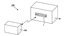
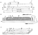
図1は、本発明のRFIDシステムを示す模式図、図2は、本発明の第1実施形態に係るRFIDタグを説明するための図であり、(a)は平面図、(b)は(a)のA−A線断面図、(c)は斜視図である。 FIG. 1 is a schematic diagram showing an RFID system of the present invention, FIG. 2 is a diagram for explaining an RFID tag according to a first embodiment of the present invention, (a) is a plan view, and (b) is ( The sectional view on the AA line of a), (c) is a perspective view.
まず、図1を参照して本発明のRFIDシステム100の概略について説明する。本発明のRFIDシステム100は、鉄鋼製品、金型や製造機器などの金属物体Mに取り付けられたRFIDタグ1と、RFIDタグ1と非接触で情報の読み書きを行うリーダライタRWとからなる。RFIDシステム100は、例えば、ステンレスなど人間が目視で識別困難な鉄鋼製品にRFIDタグ1を取り付けて入出荷や棚卸作業において、携帯可能なリーダライタRWを用いて対象製品のピッキングや検品を行なったり、金型や製造機器にRFIDタグ1を取り付けて、棚卸や使用する際の現品確認を行なう際などに利用される。
First, the outline of the
なお、本発明のRFIDシステム100においては、リーダライタRWは携帯可能なものでも固定式のものでも適用可能であるし、リーダライタRWは、リーダであってもよい。
In the
次に図2を参照してRFIDタグ1の構成について説明する。 Next, the configuration of the RFID tag 1 will be described with reference to FIG.
図2に示すように、RFIDタグ1は、接地導体板2、第1の誘電体基板3、アンテナ部4、第2の誘電体基板5、ICチップ6及びビア7から構成されている。
As shown in FIG. 2, the RFID tag 1 includes a ground conductor plate 2, a first
接地導体板2は、銅、アルミ、ステンレス等からなる導電性材料からなり、接地導体板2の上面(一の面)には、第1の誘電体基板3が積層されている。
The ground conductor plate 2 is made of a conductive material made of copper, aluminum, stainless steel, or the like, and the first
第1の誘電体基板3は、ポリエチレン、ポリエチレンテフタレート(PET)、ポリプロピレン、ポリイミド等の合成樹脂材を板状に形成してなり、第1の誘電体基板3の上面には、アンテナ部4が設けられている。
The first
アンテナ部4は、例えば、銅、アルミ、ステンレス等の金属打ち抜き加工、若しくはエッチング加工により形成される。アンテナ部4は、離間する第1のアンテナ導体部4Aと第2のアンテナ導体部4Bとからなり、第1のアンテナ導体部4Aと第2のアンテナ導体部4Bとの間にはICチップ6が実装され、ICチップ6により第1のアンテナ導体部4Aと第2のアンテナ導体部4Bとが接続される。第1のアンテナ導体部4Aと接地導体板2とはビア7により電気的に接続される。なお、ここでは、第1のアンテナ導体部4Aが短尺状に形成され、他方、第2のアンテナ導体部4Bが長尺状に形成されているが、第1のアンテナ導体部4Aと第2のアンテナ導体部4Bとは長さが等しくてもよい。
The antenna unit 4 is formed by, for example, a metal punching process such as copper, aluminum, stainless steel, or an etching process. The antenna portion 4 includes a first
第2の誘電体基板5は、ポリエチレン、ポリエチレンテフタレート(PET)、ポリプロピレン、ポリイミド等の合成樹脂材を板状に形成してなり、接地導体板2の下面(他の面)に設けられる。
The second
図2(a)に示すように、アンテナ部4の直線距離L1は、高周波の実行波長=λgに対し、λg/2に、接地導体板2の長さL2は、低周波の実行波長=λg´に対し、λg´/2に設定されることが好適である。なお、ここでは、L1がアンテナ部4の電気長となり、L2が接地導体板2の電気長となる。 As shown in FIG. 2A, the linear distance L1 of the antenna unit 4 is λ g / 2 with respect to the high-frequency effective wavelength = λ g , and the length L2 of the ground conductor plate 2 is the low-frequency effective wavelength. = Λ g ′ is preferably set to λ g ′ / 2. Here, L1 is the electrical length of the antenna unit 4, and L2 is the electrical length of the ground conductor plate 2.
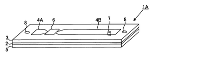
また、図2(a)に示すように、RFIDタグ1の両端部近傍には、RFIDタグ1を金属物体Mにネジ止め固着するための(図示しない)ネジを挿入する取付孔8、8が穿設されている。なお、本実施形態においては、RFIDタグをネジ止めタイプのものとしたが、これに限定されるものではなく、例えば、貼付タイプ、結束バンドなどにより取り付けるタイプのものなどでもよい。
Further, as shown in FIG. 2A, mounting
本発明者は、図1に示すように、上記構成のRFIDタグ1を金属物体Mに取り付けた状態で、RFIDタグ1の低周波側及び高周波側の電界の発生状態を調べるシミュレーションを行った。なお、本シミュレーションにおいては、低周波側の電解強度を900MHzとし、高周波側の電解強度を1GHzと設定した。すると、図2(b)に示すように(図2(b)においては、金属物体Mは略して示している)、RFIDタグ1は、次のように作用する。 As shown in FIG. 1, the present inventor performed a simulation to examine the generation state of the electric field on the low frequency side and the high frequency side of the RFID tag 1 with the RFID tag 1 having the above configuration attached to the metal object M. In this simulation, the electrolytic strength on the low frequency side was set to 900 MHz, and the electrolytic strength on the high frequency side was set to 1 GHz. Then, as shown in FIG. 2B (in FIG. 2B, the metal object M is abbreviated), the RFID tag 1 operates as follows.
高周波側においては、上層側、すなわち、アンテナ部4、第1の誘電体基板3及び接地導体板2からなる部分が、いわゆる逆L型アンテナとして機能し、この逆L型アンテナを中心に電界を放射していた。一方、低周波側においては、下層側、すなわち、接地導体板2、第2の誘電体基板5及び金属物体Mからなる部分が、いわゆるパッチアンテナとして機能し、このパッチアンテナを中心に電界を放射していた。
On the high frequency side, the upper layer side, that is, the portion composed of the antenna unit 4, the first
本シミュレーションの結果、RFIDタグ1のように構成することにより、広帯域性が確保されるとともに、接地導体板2が放射素子として機能し、高利得化も同時に実現できることが判明した。 As a result of this simulation, it has been found that the configuration like the RFID tag 1 ensures wide bandwidth, the ground conductor plate 2 functions as a radiating element, and can achieve high gain at the same time.
また、本発明者は、従来からあるパッチアンテナを用いたRFIDタグと、本発明に係るRFIDタグ1と比較するために本発明者が製造した逆L型アンテナを用いたRFIDタグ(図9参照)と、本発明に係るRFIDタグ1と、を使用して、広帯域特性の比較をすべくシミュレーションを行った。その結果を示したものが図10のグラフである。 In addition, the inventor of the present invention has compared an RFID tag using a conventional patch antenna with an RFID tag using an inverted L antenna manufactured by the inventor for comparison with the RFID tag 1 according to the present invention (see FIG. 9). ) And the RFID tag 1 according to the present invention, a simulation was performed to compare broadband characteristics. The graph of FIG. 10 shows the result.
図10においては、横軸を周波数(MHz)、縦軸をRFIDタグの起動電力(dBm)とし、起動電力が低いほうが長距離通信可能であることを示している。図10において、AIRとは、RFIDタグを金属物体以外の物体に取り付けた場合あるいは何も取り付けない場合であり、Metalとは、RFIDタグを金属物体に取り付けた場合である。また、逆Lとは図9に示す逆L型アンテナを用いたRFIDタグ、パッチとはパッチアンテナを用いたRFIDタグ、逆L改とは本発明に係るRFIDタグ1をそれぞれ示す。従って、例えば、逆L改(AIR)とは、本発明に係るRFIDタグ1を金属物体以外の物体に取り付けた場合あるいは何にも取り付けない場合(以下、このような状態を「空気中」という)であり、逆L改(Metal)とは、本発明に係るRFIDタグ1を金属物体に取り付けた場合を示す。 In FIG. 10, the horizontal axis represents the frequency (MHz) and the vertical axis represents the RFID tag activation power (dBm), which indicates that the lower the activation power, the longer distance communication is possible. In FIG. 10, AIR is a case where the RFID tag is attached to an object other than a metal object or nothing is attached, and Metal is a case where the RFID tag is attached to a metal object. Further, reverse L indicates an RFID tag using the reverse L-type antenna shown in FIG. 9, patch indicates an RFID tag using a patch antenna, and reverse L modification indicates the RFID tag 1 according to the present invention. Therefore, for example, reverse L reform (AIR) is a case where the RFID tag 1 according to the present invention is attached to an object other than a metal object or not attached to anything (hereinafter, such a state is referred to as “in the air”). The reverse L reform (Metal) indicates a case where the RFID tag 1 according to the present invention is attached to a metal object.
この結果から明らかなように、空気中においては、逆L型アンテナを用いたRFIDタグと同程度の帯域特性を有し、金属物体に取り付けた場合においては、パッチアンテナを用いたRFIDタグと同程度の高利得性を有する。すなわち、本発明に係るRFIDタグ1においては、上記のように構成したことから、逆L型アンテナ及びパッチアンテナの双方の機能を有し、広い周波数に渡って長距離通信が可能であり、広帯域化が図れ、その結果、金属面への取り付けも含め、長距離通信が各国周波数で対応可能となる。 As is clear from this result, in the air, it has the same band characteristics as an RFID tag using an inverted L-type antenna, and when attached to a metal object, it is the same as an RFID tag using a patch antenna. High gain performance. That is, since the RFID tag 1 according to the present invention is configured as described above, it has both functions of an inverted L-type antenna and a patch antenna, and can perform long-distance communication over a wide frequency range. As a result, long-distance communication, including attachment to metal surfaces, can be handled at each country's frequency.
次に、本発明の他の実施形態について図3〜図7を参照して説明する。なお、上記第1実施形態に係るRFIDタグ1と相違する点を重点的に説明し、同一の構成については同一の符号を付し詳細な説明は省略する。 Next, another embodiment of the present invention will be described with reference to FIGS. Note that differences from the RFID tag 1 according to the first embodiment will be mainly described, and the same components will be denoted by the same reference numerals and detailed description thereof will be omitted.
図3は、本発明の第2実施形態に係るRFIDタグの斜視図、図4は、本発明の第3実施形態に係るRFIDタグの斜視図、図5は、逆L型アンテナ側のアンテナ部の他の実施形態を示す平面図、図6は、逆L型アンテナ側のアンテナ部の他の実施形態を示す平面図、図7は、パッチアンテナ側のアンテナ部(接地導体板)の他の実施形態を説明するための図であり、(a)はRFIDタグにおける接地導体板の状況を示す平面図、(b)は接地導体板の平面図である。 3 is a perspective view of an RFID tag according to the second embodiment of the present invention, FIG. 4 is a perspective view of the RFID tag according to the third embodiment of the present invention, and FIG. 5 is an antenna portion on the inverted L-type antenna side. FIG. 6 is a plan view showing another embodiment of the antenna portion on the inverted L-shaped antenna side, and FIG. 7 is another view of the antenna portion (grounding conductor plate) on the patch antenna side. It is a figure for demonstrating embodiment, (a) is a top view which shows the condition of the grounding conductor board in a RFID tag, (b) is a top view of a grounding conductor board.
<第2実施形態>
第2実施形態に係るRFIDタグ1Aは、第1実施形態に係るRFIDタグ1において、ビア7の位置を第2のアンテナ導体部4B側に移動して接地導体板2とビア7により接続したものである。その他の構成は、RFIDタグ1と同様である。
<Second Embodiment>
The
<第3実施形態>
第3実施形態に係るRFIDタグ1Bは、第1実施形態に係るRFIDタグ1のように、アンテナ部4と接地導体板2とをビア7により接続するのではなく、第1のアンテナ導体部40Aの一端40A−1側を折り曲げて形成することにより第1のアンテナ導体部40Aと接地導体板2とを接続する。このような構成は次のようにして加工することにより実現可能である。例えば、一枚の導体板を角型(コの字状)に折り曲げる。この際、第1の誘電体基板3を内側に巻き込むようにする。この状態で、第1の誘電体基板3の上面側をエッチング加工し、第1のアンテナ導体部40Aと第2のアンテナ導体部4Bが形成されるようにする。なお、このように構成するときには、RFIDタグ1Bを金属物体Mに取り付けるための取付孔8は、図4のようにRFIDタグ1Bの四方に形成されるようにするとよい。
<Third Embodiment>
As in the RFID tag 1 according to the first embodiment, the
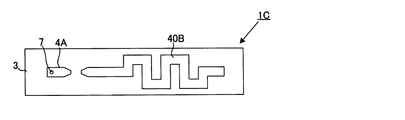
<第4実施形態〜第6実施形態>
第4実施形態〜第6実施形態におけるRFIDタグの構成を概略すると、第4実施形態及び第5実施形態に係るRFIDタグ1C、1Dは、RFIDタグ1のアンテナ部4の形状に手を加えたものであり、第5実施形態に係るRFIDタグ1Eは、RFIDタグ1の接地導体板2の形状に手を加えたものである。なお、図5〜図7においては、これら相違点さえ分かればよいとの趣旨から、簡略化して図示してある。
<Fourth Embodiment to Sixth Embodiment>
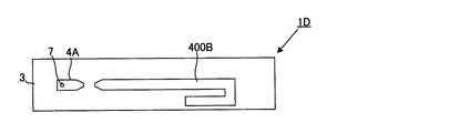
When the configuration of the RFID tag in the fourth to sixth embodiments is outlined, the RFID tags 1C and 1D according to the fourth and fifth embodiments are modified in the shape of the antenna unit 4 of the RFID tag 1. The
具体的に説明すると、RFIDタグ1Cにおいては、第2のアンテナ導体部の形状を図5に示すようにメアンダ状に形成した第2のアンテナ導体部40Bを用いている点が上記RFIDタグ1の構成と相違する。他方、RFIDタグ1Dにおいては、第2のアンテナ導体部の形状を図6に示すように端部側をつづら折り状に矩形に折り返して形成した第2のアンテナ導体部400Bを用いている点が上記RFIDタグ1の構成と相違する。その他の構成は上記RFIDタグ1と同様である。このように形成することにより、RFIDタグ全体の小型化が図れる。
More specifically, the RFID tag 1C uses the second
一方、RFIDタグ1Eにおいては、接地導体板2の形状を図7(b)に示すようにノッチN1、N2を形成することにより接地導体板全体をメアンダ状に形成した接地導体板20を用いている点が上記RFIDタグ1の構成と相違する点である。その他の構成は上記RFIDタグ1と同様である。このように形成することにより、RFIDタグ全体の小型化が図れる。
On the other hand, in the
なお、図5に示すアンテナ部(4A及び40Bからなる部分)及び図7(b)に示す接地導体板20の双方を使用してRFIDタグを製造してもよい。このようにすることにより、更なるRFIDタグの小型化が図れる。
In addition, you may manufacture an RFID tag using both the antenna part (part which consists of 4A and 40B) shown in FIG. 5, and the
次に本発明に係るRFIDタグセットの構成について図8を参照して説明する。 Next, the configuration of the RFID tag set according to the present invention will be described with reference to FIG.
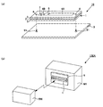
図8は、本発明のRFIDタグセットを説明するための図であり、(a)はRFIDタグセットの構造を説明するための斜視図、(b)はRFIDタグセットの使用状態を説明するための模式図である。 8A and 8B are diagrams for explaining the RFID tag set of the present invention, in which FIG. 8A is a perspective view for explaining the structure of the RFID tag set, and FIG. 8B is a diagram for explaining a use state of the RFID tag set. FIG.
本発明のRFIDタグセット10は、要するに、上記説明した第1実施形態〜第5実施形態に係るRFIDタグにおいて、予め導体板9を設けた構成である。すなわち、上記第1実施形態〜第5実施形態に係るRFIDタグにおいては、いずれも、取付対象である金属物体Mの金属面をパッチアンテナ側の接地導体として機能させることにより、その下層側において、パッチアンテナと同様の機能を発揮させるようにしていた。しかしながら、本実施形態におけるRFIDタグセット10においては、予め導体板9を上記第1実施形態〜第5実施形態に係るRFIDタグのいずれかと取り外し可能に構成することにより、取付対象の属性(金属物体であるか否か)に関係なく、常に逆L型アンテナ及びパッチアンテナの双方の機能を発揮することが可能となる。
In short, the RFID tag set 10 of the present invention has a configuration in which the
このようなRFIDタグセット10としては、上記説明したRFIDタグ1と、RFIDタグ1の2つの取付孔8、8の位置に対応して2つの取付孔91、91を穿設した導体板9とからなる。導体板9は、図8(a)(b)に示すように、2つの取付孔91、91と2つの取付孔8、8の位置を合わせた状態で、(図示しない)ネジにより、RFIDタグ1と物体M1との間に介在させるようにして取り付けられる。このRFIDタグ10を用いても上記RFIDシステム100と同様のシステムであるRFIDシステム100Aの運用が可能である。
As such an RFID tag set 10, the above-described RFID tag 1, and a
なお、導体板9は、パッチアンテナの接地導体として機能することから、RFIDタグ1の大きさに比して大きめに形成するとRFIDタグ1とリーダライタRW間の通信が安定する。
Since the
1、1A、1B、1C、1D、1E RFIDタグ
2、20 接地導体板
3 第1の誘電体基板
4 アンテナ部
4A、40A 第1のアンテナ導体部
4B、40B、400B 第2のアンテナ導体部
5 第2の誘電体基板
6 ICチップ
7 ビア(接続部)
8 取付孔
9 導体板
10 RFIDタグセット
100、100A RFIDシステム
L1 アンテナ部の直線距離
L2 設置導体板の長さ
M コンテナ
RW リーダライタ
1, 1A, 1B, 1C, 1D,
8 Mounting
Claims (9)
該接地導体板の一の面に積層された第1の誘電体基板と、
該第1の誘電体基板上に設けられた第1のアンテナ導体部及び第2のアンテナ導体部からなるアンテナ部と、
該第1のアンテナ導体部と第2のアンテナ導体部とを接続するICチップと、
前記第1のアンテナ導体部あるいは第2のアンテナ導体部のいずれか一方と前記接地導体板とを接続する接続部と、
前記接地導体板の他の面に設けられた第2の誘電体基板と、を有するとともに、
前記アンテナ部の電気長と前記接地導体板の電気長とが相違すること
を特徴とするRFIDタグ。 A grounding conductor plate;
A first dielectric substrate laminated on one surface of the ground conductor plate;
An antenna portion comprising a first antenna conductor portion and a second antenna conductor portion provided on the first dielectric substrate;
An IC chip connecting the first antenna conductor portion and the second antenna conductor portion;
A connecting portion for connecting either the first antenna conductor portion or the second antenna conductor portion and the ground conductor plate;
A second dielectric substrate provided on the other surface of the ground conductor plate, and
An RFID tag, wherein an electrical length of the antenna portion is different from an electrical length of the ground conductor plate.
該RFIDタグセットは、
前記導体板が、前記RFIDタグと前記物体との間に介在した状態で物体に取り付けられることを特徴とするRFIDタグセット。 An RFID tag set comprising: the RFID tag according to any one of claims 1 to 6; and a conductor plate connectable to the RFID tag.
The RFID tag set is
An RFID tag set, wherein the conductor plate is attached to an object in a state of being interposed between the RFID tag and the object.
Priority Applications (5)
| Application Number | Priority Date | Filing Date | Title |
|---|---|---|---|
| JP2008228819A JP4618459B2 (en) | 2008-09-05 | 2008-09-05 | RFID tag, RFID tag set and RFID system |
| EP09811465A EP2330684B1 (en) | 2008-09-05 | 2009-08-31 | Rfid tag, rfid tag set and rfid system |
| CN2009801347420A CN102144332B (en) | 2008-09-05 | 2009-08-31 | RFID tag, RFID tag set and RFID system |
| PCT/JP2009/065163 WO2010026939A1 (en) | 2008-09-05 | 2009-08-31 | Rfid tag, rfid tag set and rfid system |
| US13/062,034 US20110227710A1 (en) | 2008-09-05 | 2009-08-31 | Rfid tag, rfid tag set and rfid system |
Applications Claiming Priority (1)
| Application Number | Priority Date | Filing Date | Title |
|---|---|---|---|
| JP2008228819A JP4618459B2 (en) | 2008-09-05 | 2008-09-05 | RFID tag, RFID tag set and RFID system |
Publications (2)
| Publication Number | Publication Date |
|---|---|
| JP2010063017A true JP2010063017A (en) | 2010-03-18 |
| JP4618459B2 JP4618459B2 (en) | 2011-01-26 |
Family
ID=41797107
Family Applications (1)
| Application Number | Title | Priority Date | Filing Date |
|---|---|---|---|
| JP2008228819A Active JP4618459B2 (en) | 2008-09-05 | 2008-09-05 | RFID tag, RFID tag set and RFID system |
Country Status (5)
| Country | Link |
|---|---|
| US (1) | US20110227710A1 (en) |
| EP (1) | EP2330684B1 (en) |
| JP (1) | JP4618459B2 (en) |
| CN (1) | CN102144332B (en) |
| WO (1) | WO2010026939A1 (en) |
Cited By (4)
| Publication number | Priority date | Publication date | Assignee | Title |
|---|---|---|---|---|
| JP2014127752A (en) * | 2012-12-25 | 2014-07-07 | Smart:Kk | Antenna and system using the same |
| WO2019077926A1 (en) * | 2017-10-20 | 2019-04-25 | 株式会社フェニックスソリューション | Dual rf tag |
| WO2020075321A1 (en) * | 2018-10-10 | 2020-04-16 | オムロン株式会社 | Antenna device |
| WO2020075320A1 (en) * | 2018-10-10 | 2020-04-16 | オムロン株式会社 | Electronic apparatus |
Families Citing this family (54)
| Publication number | Priority date | Publication date | Assignee | Title |
|---|---|---|---|---|
| US7519328B2 (en) | 2006-01-19 | 2009-04-14 | Murata Manufacturing Co., Ltd. | Wireless IC device and component for wireless IC device |
| US9064198B2 (en) | 2006-04-26 | 2015-06-23 | Murata Manufacturing Co., Ltd. | Electromagnetic-coupling-module-attached article |
| US8235299B2 (en) | 2007-07-04 | 2012-08-07 | Murata Manufacturing Co., Ltd. | Wireless IC device and component for wireless IC device |
| CN104078767B (en) | 2007-07-09 | 2015-12-09 | 株式会社村田制作所 | Wireless IC device |
| WO2009011400A1 (en) | 2007-07-17 | 2009-01-22 | Murata Manufacturing Co., Ltd. | Wireless ic device and electronic apparatus |
| WO2009011423A1 (en) | 2007-07-18 | 2009-01-22 | Murata Manufacturing Co., Ltd. | Wireless ic device |
| JP5267463B2 (en) | 2008-03-03 | 2013-08-21 | 株式会社村田製作所 | Wireless IC device and wireless communication system |
| CN103729676B (en) | 2008-05-21 | 2017-04-12 | 株式会社村田制作所 | Wireless ic device |
| WO2009145007A1 (en) | 2008-05-26 | 2009-12-03 | 株式会社村田製作所 | Wireless ic device system and method for authenticating wireless ic device |
| EP2320519B1 (en) | 2008-08-19 | 2017-04-12 | Murata Manufacturing Co., Ltd. | Wireless ic device and method for manufacturing same |
| CN104362424B (en) | 2008-11-17 | 2018-09-21 | 株式会社村田制作所 | Wireless telecom equipment |
| CN103500873B (en) | 2009-01-09 | 2016-08-31 | 株式会社村田制作所 | Wireless ic device and wireless ic module |
| CN102301528B (en) | 2009-01-30 | 2015-01-28 | 株式会社村田制作所 | Antenna and wireless ic device |
| JP5510450B2 (en) | 2009-04-14 | 2014-06-04 | 株式会社村田製作所 | Wireless IC device |
| WO2010122685A1 (en) | 2009-04-21 | 2010-10-28 | 株式会社村田製作所 | Antenna apparatus and resonant frequency setting method of same |
| JP5201270B2 (en) | 2009-09-30 | 2013-06-05 | 株式会社村田製作所 | Circuit board and manufacturing method thereof |
| JP5304580B2 (en) | 2009-10-02 | 2013-10-02 | 株式会社村田製作所 | Wireless IC device |
| WO2011052310A1 (en) | 2009-10-27 | 2011-05-05 | 株式会社村田製作所 | Transmitting/receiving apparatus and wireless tag reader |
| JP5327334B2 (en) | 2009-11-04 | 2013-10-30 | 株式会社村田製作所 | Communication terminal and information processing system |
| WO2011055701A1 (en) | 2009-11-04 | 2011-05-12 | 株式会社村田製作所 | Communication terminal and information processing system |
| WO2011062238A1 (en) | 2009-11-20 | 2011-05-26 | 株式会社村田製作所 | Antenna device and mobile communication terminal |
| GB2488450B (en) | 2009-12-24 | 2014-08-20 | Murata Manufacturing Co | Antenna and mobile terminal |
| CN102792520B (en) | 2010-03-03 | 2017-08-25 | 株式会社村田制作所 | Wireless communication module and Wireless Telecom Equipment |
| CN102782937B (en) | 2010-03-03 | 2016-02-17 | 株式会社村田制作所 | Wireless communication devices and wireless communication terminal |
| WO2011111509A1 (en) | 2010-03-12 | 2011-09-15 | 株式会社村田製作所 | Radio communication device and metallic article |
| US20110231236A1 (en) * | 2010-03-19 | 2011-09-22 | Felipe Gonzalez | Coupon System and Method |
| WO2011118379A1 (en) | 2010-03-24 | 2011-09-29 | 株式会社村田製作所 | Rfid system |
| WO2011122163A1 (en) | 2010-03-31 | 2011-10-06 | 株式会社村田製作所 | Antenna and wireless communication device |
| JP5376060B2 (en) | 2010-07-08 | 2013-12-25 | 株式会社村田製作所 | Antenna and RFID device |
| WO2012014939A1 (en) | 2010-07-28 | 2012-02-02 | 株式会社村田製作所 | Antenna device and communications terminal device |
| JP5423897B2 (en) | 2010-08-10 | 2014-02-19 | 株式会社村田製作所 | Printed wiring board and wireless communication system |
| WO2012043432A1 (en) | 2010-09-30 | 2012-04-05 | 株式会社村田製作所 | Wireless ic device |
| JP5758909B2 (en) | 2010-10-12 | 2015-08-05 | 株式会社村田製作所 | Communication terminal device |
| WO2012053412A1 (en) | 2010-10-21 | 2012-04-26 | 株式会社村田製作所 | Communication terminal device |
| JP5510560B2 (en) | 2011-01-05 | 2014-06-04 | 株式会社村田製作所 | Wireless communication device |
| JP5304956B2 (en) | 2011-01-14 | 2013-10-02 | 株式会社村田製作所 | RFID chip package and RFID tag |
| CN103119786B (en) | 2011-02-28 | 2015-07-22 | 株式会社村田制作所 | Wireless communication device |
| WO2012121185A1 (en) | 2011-03-08 | 2012-09-13 | 株式会社村田製作所 | Antenna device and communication terminal apparatus |
| WO2012137717A1 (en) | 2011-04-05 | 2012-10-11 | 株式会社村田製作所 | Wireless communication device |
| JP5482964B2 (en) | 2011-04-13 | 2014-05-07 | 株式会社村田製作所 | Wireless IC device and wireless communication terminal |
| WO2012157596A1 (en) | 2011-05-16 | 2012-11-22 | 株式会社村田製作所 | Wireless ic device |
| WO2013008874A1 (en) | 2011-07-14 | 2013-01-17 | 株式会社村田製作所 | Wireless communication device |
| DE112012001977T5 (en) | 2011-07-15 | 2014-02-20 | Murata Manufacturing Co., Ltd. | Radio communication equipment |
| JP5660217B2 (en) | 2011-07-19 | 2015-01-28 | 株式会社村田製作所 | Antenna device, RFID tag, and communication terminal device |
| CN203553354U (en) | 2011-09-09 | 2014-04-16 | 株式会社村田制作所 | Antenna device and wireless device |
| JP5344108B1 (en) | 2011-12-01 | 2013-11-20 | 株式会社村田製作所 | Wireless IC device and manufacturing method thereof |
| JP5354137B1 (en) | 2012-01-30 | 2013-11-27 | 株式会社村田製作所 | Wireless IC device |
| WO2013125610A1 (en) | 2012-02-24 | 2013-08-29 | 株式会社村田製作所 | Antenna device and wireless communication device |
| JP5304975B1 (en) | 2012-04-13 | 2013-10-02 | 株式会社村田製作所 | RFID tag inspection method and inspection apparatus |
| WO2016018585A1 (en) * | 2014-07-31 | 2016-02-04 | 3M Innovative Properties Company | Rfid tag on stretchable substrate |
| US11213773B2 (en) | 2017-03-06 | 2022-01-04 | Cummins Filtration Ip, Inc. | Genuine filter recognition with filter monitoring system |
| FR3082361B1 (en) | 2018-06-12 | 2021-04-23 | Continental Automotive France | USER APPROACH AND / OR CONTACT DETECTION AND ULTRA HIGH FREQUENCY COMMUNICATION SYSTEM WITH USER PORTABLE EQUIPMENT |
| JP6750758B1 (en) | 2019-03-06 | 2020-09-02 | 株式会社村田製作所 | RFID tags and articles with RFID tags |
| WO2020179131A1 (en) * | 2019-03-06 | 2020-09-10 | 株式会社村田製作所 | Rfid tag and article with rfid tag |
Citations (9)
| Publication number | Priority date | Publication date | Assignee | Title |
|---|---|---|---|---|
| JP2000332523A (en) * | 1999-05-24 | 2000-11-30 | Hitachi Ltd | Radio tag, and its manufacture and arrangement |
| JP2001101365A (en) * | 1999-09-27 | 2001-04-13 | Matsushita Electric Ind Co Ltd | Non-contact ic card and mobile object identifying system |
| JP2001175823A (en) * | 1999-12-16 | 2001-06-29 | Seiko Precision Inc | Noncontact id tag |
| JP2005191705A (en) * | 2003-12-24 | 2005-07-14 | Sharp Corp | Wireless tag and rfid system employing the same |
| WO2006049068A1 (en) * | 2004-11-08 | 2006-05-11 | Matsushita Electric Industrial Co., Ltd. | Antenna assembly and wireless communication system employing same |
| WO2006075398A1 (en) * | 2005-01-17 | 2006-07-20 | Fujitsu Limited | Communication device and communication method |
| JP2006264760A (en) * | 2005-03-25 | 2006-10-05 | Toshiba Tec Corp | Case and radio tag reading system |
| JP2006338361A (en) * | 2005-06-02 | 2006-12-14 | Ajinomoto Co Inc | Rfid tag-installing device, rfid tag-installing carriage, rfid tag-installing box, communication equipment and communication method |
| JP2007028002A (en) * | 2005-07-13 | 2007-02-01 | Matsushita Electric Ind Co Ltd | Antenna of reader/writer, and communication system |
Family Cites Families (16)
| Publication number | Priority date | Publication date | Assignee | Title |
|---|---|---|---|---|
| JP3141692B2 (en) * | 1994-08-11 | 2001-03-05 | 松下電器産業株式会社 | Millimeter wave detector |
| US6751493B2 (en) * | 2002-01-09 | 2004-06-15 | Unilead International, Inc. | Universal electrocardiogram sensor positioning mask with repositionable sensors and method for employing same |
| SG115459A1 (en) * | 2002-03-04 | 2005-10-28 | Micron Technology Inc | Flip chip packaging using recessed interposer terminals |
| WO2005083838A1 (en) * | 2004-02-27 | 2005-09-09 | Fujitsu Limited | Radio tag |
| US7605706B2 (en) * | 2005-05-13 | 2009-10-20 | The Kennedy Group, Inc. | Patch antenna for RFID tag |
| JP4500214B2 (en) * | 2005-05-30 | 2010-07-14 | 株式会社日立製作所 | Wireless IC tag and method of manufacturing wireless IC tag |
| KR100714489B1 (en) * | 2005-06-20 | 2007-05-04 | 주식회사 오성전자 | Meandered slit antenna |
| KR100764105B1 (en) * | 2006-02-28 | 2007-10-08 | 주식회사 손텍 | radio frequency identification tag and ceramic patch antenna for radio frequency identification system |
| JP4363409B2 (en) | 2006-03-06 | 2009-11-11 | 三菱電機株式会社 | RFID tag and manufacturing method thereof |
| EP1993170A4 (en) * | 2006-03-06 | 2011-11-16 | Mitsubishi Electric Corp | Rfid tag, method for manufacturing rfid tag and method for arranging rfid tag |
| CN101454788A (en) * | 2006-05-31 | 2009-06-10 | 株式会社半导体能源研究所 | Semiconductor device and ic label, ic tag, and ic card having the same |
| GB0611983D0 (en) * | 2006-06-16 | 2006-07-26 | Qinetiq Ltd | Electromagnetic radiation decoupler |
| JP5057786B2 (en) * | 2006-08-09 | 2012-10-24 | 富士通株式会社 | tag |
| US7768457B2 (en) * | 2007-06-22 | 2010-08-03 | Vubiq, Inc. | Integrated antenna and chip package and method of manufacturing thereof |
| WO2009001158A1 (en) * | 2007-06-22 | 2008-12-31 | Nokia Corporation | An antenna arrangement |
| JP5086004B2 (en) * | 2007-08-30 | 2012-11-28 | 富士通株式会社 | Tag antenna and tag |
-
2008
- 2008-09-05 JP JP2008228819A patent/JP4618459B2/en active Active
-
2009
- 2009-08-31 WO PCT/JP2009/065163 patent/WO2010026939A1/en active Application Filing
- 2009-08-31 CN CN2009801347420A patent/CN102144332B/en active Active
- 2009-08-31 US US13/062,034 patent/US20110227710A1/en not_active Abandoned
- 2009-08-31 EP EP09811465A patent/EP2330684B1/en active Active
Patent Citations (9)
| Publication number | Priority date | Publication date | Assignee | Title |
|---|---|---|---|---|
| JP2000332523A (en) * | 1999-05-24 | 2000-11-30 | Hitachi Ltd | Radio tag, and its manufacture and arrangement |
| JP2001101365A (en) * | 1999-09-27 | 2001-04-13 | Matsushita Electric Ind Co Ltd | Non-contact ic card and mobile object identifying system |
| JP2001175823A (en) * | 1999-12-16 | 2001-06-29 | Seiko Precision Inc | Noncontact id tag |
| JP2005191705A (en) * | 2003-12-24 | 2005-07-14 | Sharp Corp | Wireless tag and rfid system employing the same |
| WO2006049068A1 (en) * | 2004-11-08 | 2006-05-11 | Matsushita Electric Industrial Co., Ltd. | Antenna assembly and wireless communication system employing same |
| WO2006075398A1 (en) * | 2005-01-17 | 2006-07-20 | Fujitsu Limited | Communication device and communication method |
| JP2006264760A (en) * | 2005-03-25 | 2006-10-05 | Toshiba Tec Corp | Case and radio tag reading system |
| JP2006338361A (en) * | 2005-06-02 | 2006-12-14 | Ajinomoto Co Inc | Rfid tag-installing device, rfid tag-installing carriage, rfid tag-installing box, communication equipment and communication method |
| JP2007028002A (en) * | 2005-07-13 | 2007-02-01 | Matsushita Electric Ind Co Ltd | Antenna of reader/writer, and communication system |
Cited By (5)
| Publication number | Priority date | Publication date | Assignee | Title |
|---|---|---|---|---|
| JP2014127752A (en) * | 2012-12-25 | 2014-07-07 | Smart:Kk | Antenna and system using the same |
| WO2019077926A1 (en) * | 2017-10-20 | 2019-04-25 | 株式会社フェニックスソリューション | Dual rf tag |
| JPWO2019077926A1 (en) * | 2017-10-20 | 2020-11-19 | 株式会社フェニックスソリューション | Dual RF tag |
| WO2020075321A1 (en) * | 2018-10-10 | 2020-04-16 | オムロン株式会社 | Antenna device |
| WO2020075320A1 (en) * | 2018-10-10 | 2020-04-16 | オムロン株式会社 | Electronic apparatus |
Also Published As
| Publication number | Publication date |
|---|---|
| EP2330684A4 (en) | 2011-10-19 |
| WO2010026939A1 (en) | 2010-03-11 |
| CN102144332A (en) | 2011-08-03 |
| JP4618459B2 (en) | 2011-01-26 |
| US20110227710A1 (en) | 2011-09-22 |
| CN102144332B (en) | 2013-12-11 |
| EP2330684A1 (en) | 2011-06-08 |
| EP2330684B1 (en) | 2013-03-27 |
Similar Documents
| Publication | Publication Date | Title |
|---|---|---|
| JP4618459B2 (en) | RFID tag, RFID tag set and RFID system | |
| JP5703977B2 (en) | Metal articles with wireless communication devices | |
| JP5526726B2 (en) | Wireless tag | |
| US8599074B2 (en) | Mobile communication device and antenna thereof | |
| US8779985B2 (en) | Dual radiator monopole antenna | |
| JP2008182438A (en) | Radio tag | |
| US7821469B2 (en) | Printed antenna | |
| JP2007104211A (en) | Antenna, wireless device, antenna design method, and method for measuring antenna operating frequency | |
| US20110148722A1 (en) | Compact circular polarized monopole and slot uhf rfid antenna systems and methods | |
| JP2012253699A (en) | Wireless communication device, its manufacturing method, and metal article with wireless communication device | |
| KR101070486B1 (en) | Radio Frequency Identification Tag | |
| TWI518989B (en) | Circularly polarized antenna | |
| US9755307B2 (en) | Antenna structure and wireless communication device employing same | |
| US20190157747A1 (en) | Planar rf antenna with duplicate unit cells | |
| JP5187083B2 (en) | RFID tag, RFID system, and RFID tag manufacturing method | |
| KR101965227B1 (en) | Apparatus for antenna | |
| US9306269B2 (en) | Electronic apparatus with radio antenna folded in a casing | |
| JP2012252664A (en) | Radio communication device, manufacturing method thereof, and metal article with radio communication device | |
| JPWO2011080904A1 (en) | Antenna device | |
| JP5112192B2 (en) | Antenna and RFID reader | |
| US9460379B2 (en) | RF tag with resonant circuit structure | |
| JP6729843B1 (en) | RFID tag | |
| TWI536673B (en) | Dipole antenna for rfid tag | |
| US8130151B2 (en) | Monopole antenna with ultra wide band | |
| JP2008236713A (en) | Antenna for radio frequency identification tag |
Legal Events
| Date | Code | Title | Description |
|---|---|---|---|
| A521 | Request for written amendment filed |
Free format text: JAPANESE INTERMEDIATE CODE: A523 Effective date: 20100112 |
|
| TRDD | Decision of grant or rejection written | ||
| A01 | Written decision to grant a patent or to grant a registration (utility model) |
Free format text: JAPANESE INTERMEDIATE CODE: A01 Effective date: 20100929 |
|
| A01 | Written decision to grant a patent or to grant a registration (utility model) |
Free format text: JAPANESE INTERMEDIATE CODE: A01 |
|
| A61 | First payment of annual fees (during grant procedure) |
Free format text: JAPANESE INTERMEDIATE CODE: A61 Effective date: 20101012 |
|
| FPAY | Renewal fee payment (event date is renewal date of database) |
Free format text: PAYMENT UNTIL: 20131105 Year of fee payment: 3 |
|
| R150 | Certificate of patent or registration of utility model |
Ref document number: 4618459 Country of ref document: JP Free format text: JAPANESE INTERMEDIATE CODE: R150 Free format text: JAPANESE INTERMEDIATE CODE: R150 |