JP2010056499A - Method of manufacturing multilayer circuit board, and multilayer circuit board - Google Patents
Method of manufacturing multilayer circuit board, and multilayer circuit board Download PDFInfo
- Publication number
- JP2010056499A JP2010056499A JP2008246431A JP2008246431A JP2010056499A JP 2010056499 A JP2010056499 A JP 2010056499A JP 2008246431 A JP2008246431 A JP 2008246431A JP 2008246431 A JP2008246431 A JP 2008246431A JP 2010056499 A JP2010056499 A JP 2010056499A
- Authority
- JP
- Japan
- Prior art keywords
- film
- electric circuit
- forming
- plating
- resin film
- Prior art date
- Legal status (The legal status is an assumption and is not a legal conclusion. Google has not performed a legal analysis and makes no representation as to the accuracy of the status listed.)
- Granted
Links
Images

Abstract
Description
本発明は、多層配線基板の製造方法及び多層配線基板に関する。 The present invention relates to a method for manufacturing a multilayer wiring board and a multilayer wiring board.
近年、電気・電子分野における配線回路の高密度化の要請に応じるべく、配線幅の細線化や配線間隔の狭化が進んでいる。 In recent years, in order to meet the demand for higher density of wiring circuits in the electric and electronic fields, the wiring width has been narrowed and the wiring interval has been narrowed.
従来から、絶縁基材に金属配線を形成する方法としては、サブトラクティブ法やアディティブ法が知られている。サブトラクティブ法は、絶縁基材表面に被着された金属箔の不要な部分を除去(サブトラクティブ)することにより、金属配線を形成したい部分の金属箔のみを残す方法である。一方、アディティブ法は、絶縁基材表面の金属配線を形成したい部分のみに無電解メッキを施す方法である。 Conventionally, a subtractive method or an additive method is known as a method for forming a metal wiring on an insulating substrate. The subtractive method is a method in which an unnecessary portion of the metal foil deposited on the surface of the insulating base material is removed (subtractive) to leave only a portion of the metal foil where the metal wiring is to be formed. On the other hand, the additive method is a method in which electroless plating is applied only to a portion where metal wiring on the surface of the insulating base material is to be formed.
サブトラクティブ法は、厚膜の金属箔をエッチングすることにより、回路形成部分のみの金属箔を残す方法である。この方法によれば、除去される部分の金属を浪費することになる。一方、アディティブ法は、金属配線を形成したい部分のみに無電解メッキ膜を形成することができるために、金属を浪費しない。 The subtractive method is a method in which only a circuit forming portion is left by etching a thick metal foil. According to this method, a portion of the metal to be removed is wasted. On the other hand, the additive method does not waste metal because the electroless plating film can be formed only on the portion where the metal wiring is to be formed.
従来の代表的なアディティブ法であるフルアディティブ法により、金属配線を形成する方法の概略について、図9(A)〜(E)の工程断面図を参照しながら説明する。 An outline of a method of forming a metal wiring by a full additive method, which is a typical representative additive method, will be described with reference to process cross-sectional views of FIGS.
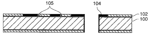
はじめに、図9(A)に示すように、スルーホール101が設けられた絶縁基材100の表面にメッキ触媒102を付着させる。なお、絶縁基材100の表面は、予め粗化されている。次に、図9(B)に示すように、フォトレジスト層103を形成する。次に、図9(C)に示すように、フォトレジスト層103の表面に所定の回路パターンが形成されたフォトマスク110を介して露光する。次に、図9(D)に示すように、回路パターンを現像する。そして、図9(E)に示すように、現像により形成された回路パターン部分及びスルーホールに無電解銅メッキを施すことにより金属配線104を形成する。このような工程により絶縁基材100の表面に電気回路が形成される。
First, as shown in FIG. 9A, a plating
このような従来のアディティブ法によれば、次のような問題が生じていた。すなわち、フォトレジスト層103がフォトマスクのパターン通りに高精度に現像された場合には、フォトレジストで保護されていない部分のみに正確にメッキ膜を形成させることができる。しかし、フォトレジスト層103が高精度に現像されなかった場合には、絶縁基材100の表面全体にメッキ触媒102が付着されているために、図10に示すような、本来メッキ膜を形成したくない部分に余分なメッキ膜105が形成されることがあった。そして、このような余分なメッキ膜105が形成された場合には、隣接する金属配線間に短絡やマイグレーションが起こりやすくなる。特に、配線間隔が狭くなるにつれて、このような問題がより発生しやすくなる。
According to such a conventional additive method, the following problems have occurred. That is, when the
このような問題を解決すべく、下記特許文献1には、絶縁基材上に保護膜をコーティングする工程と、保護膜をコーティングした絶縁基材上に機械加工あるいはレーザービームの照射により配線パターンに対応した溝及びスルーホールを形成する工程と、絶縁基材全面に活性化層を形成する工程と、保護膜を剥離して溝およびスルーホールの内壁面のみに活性化層を残す工程と、絶縁基材に残された活性化層が付着した溝およびスルーホールの内壁面のみに選択的に導電層を形成する工程とを備えた印刷配線板の製造方法が記載されている。この方法を、図11の工程断面図を参照しながら説明する。
In order to solve such a problem, the following
はじめに、図11(A)に示すように、絶縁基材200の表面に保護膜201をコーティングする。次に、図11(B)に示すように、保護膜201をコーティングした絶縁基材200上にレーザー加工により、所望の配線パターンの溝202及びスルーホール203を形成する。次に、図11(C)に示すように、溝202及びスルーホール203の表面、並びに保護膜201の表面にメッキ触媒204を付着させる。そして、図11(D)に示すように、保護膜201を剥離して、溝202およびスルーホール203の表面のみにメッキ触媒204を残す。次に、図11(E)に示すように、メッキ触媒204が残された部分のみに選択的に無電解メッキ膜を形成することにより、スルーホール203の内壁面及び溝202のみに導電層205が形成される。
First, as shown in FIG. 11A, the surface of the
ところで、近年、高密度化された多層配線基板の製造方法として、各層の回路を逐次に一層ずつ形成し、層間接続ビアを形成しながら積層するビルドアップ法が知られている。ビルドアップ法の一般的な方法を図12の工程断面図を参照しながら説明する。 By the way, in recent years, as a method of manufacturing a high-density multilayer wiring board, a build-up method is known in which circuits of each layer are sequentially formed one by one and stacked while forming interlayer connection vias. A general build-up method will be described with reference to the process cross-sectional view of FIG.
ビルドアップ法においては、はじめに、図12(A)に示すように、第1層目の絶縁基材300上に金属配線301を形成する。次に、図12(B)に示すように、絶縁基材300表面に絶縁樹脂層302を形成する。絶縁樹脂層302は、例えば、液状樹脂を塗布して硬化させたり、絶縁体フィルムを貼り合わせたりすることにより形成される。次に、図12(C)に示すように、絶縁樹脂層302にブラインドビアホール(IVH)304を形成する。IVH304はレーザー加工により形成される。レーザー加工により形成されたIVH304の底部には、図12(C)に示すように、樹脂残渣であるスミア305が残る。金属配線301は薄膜であるために、レーザー加工によりスミア305を完全に除去しようとすると、金属配線301が薄くなったり、孔が空いてしまったりするおそれがある。そのために、レーザー加工は、絶縁樹脂を完全に除去する前に終了しなければならない。このように、IVH304の底部のスミア305をレーザー加工により完全に除去することが困難である。
In the build-up method, first, as shown in FIG. 12A, the
IVH304の底部に残ったスミア305は導通不良の原因となる。このためスミア305は、デスミア処理により、図12(D)に示すように除去しなければならない。デスミア処理とは、過マンガン酸溶液等に浸漬することにより、スミア305を溶解除去する処理である。なお、デスミア処理は、絶縁樹脂層302の表面を粗化する処理を兼ねている。この粗化された表面は、絶縁樹脂層302と新たに形成される二層目の金属配線307との密着性を高める。次に、図12(E)に示すように、絶縁樹脂層302の表面にフォトレジスト層306を形成する。次に、図12(F)に示すように、フォトレジスト層306の表面に所定の回路パターンが形成された図略のフォトマスクを介して露光した後、回路パターンを現像する。そして、図12(G)に示すように、現像により形成された回路パターン部分及びスルーホールに無電解銅メッキを施すことにより金属配線307が形成される。
図12(A)〜(G)を参照して説明したようなビルドアップ法に、高精度の金属配線を形成しうる図11(A)〜(E)で説明したようなアディティブ法を適用して新たな金属配線を形成する場合、以下に説明するような問題があった。図11(A)〜(E)に記載されたアディティブ法をビルドアップ法に適用する場合の工程について、図13の工程断面図を参照しながら説明する。 The additive method as described with reference to FIGS. 11A to 11E that can form high-precision metal wiring is applied to the build-up method as described with reference to FIGS. 12A to 12G. When forming a new metal wiring, there are problems as described below. A process when the additive method described in FIGS. 11A to 11E is applied to the build-up method will be described with reference to the process cross-sectional view of FIG.
はじめに、図13(A)に示すように、絶縁基材300の表面に金属配線301を形成する。次に、図13(B)に示すように、絶縁基材300の表面に絶縁樹脂層200を形成する。次に、図13(C)に示すように、絶縁樹脂層200上に保護膜201をコーティングする。次に、レーザー加工により、図13(D)に示すように、保護膜201をコーティングした絶縁樹脂層200上に配線パターンに対応した溝202及びスルーホール203を形成する。このとき、レーザー加工により形成されたスルーホール203の底部にはスミア305が残る。スミア305は、導通不良の原因になるために除去しなければならない。しかしながら、保護膜201の形成後にデスミア処理する場合、図13(E)に示すようにスミア305とともに保護膜201も膨潤又は溶解してしまうという問題があった。また、メッキ触媒を付着させた後、デスミア処理をする場合には、金属配線を形成しようとする部分のメッキ触媒が遊離してしまうという問題があった。従って、図12(A)〜(E)で説明したようなアディティブ法をビルドアップ法に適用した方法では、高精度な金属配線を有する多層配線基板が得られなかった。
First, as shown in FIG. 13A, the
本発明は、上記問題点を解決するものであり、ビルドアップ法により金属配線を積層して多層配線基板を製造するに際して、形状精度の高い金属配線が積層形成された多層配線基板を提供することを目的とする。 The present invention solves the above-described problems, and provides a multilayer wiring board in which metal wirings with high shape accuracy are laminated when a multilayer wiring board is manufactured by stacking metal wirings by a build-up method. With the goal.
本発明の多層配線基板の製造方法は、第一電気回路の所定位置に突設された導体柱を埋設させるように絶縁層が形成されてなる導体柱含有回路基板の、前記導体柱の突設側の絶縁層表面に樹脂皮膜を形成する皮膜形成工程と、前記樹脂皮膜の外表面側からレーザー加工することにより、少なくとも前記樹脂皮膜の厚み分以上の深さの回路溝を形成する回路溝形成工程と、前記樹脂皮膜の外表面側からレーザー加工することにより、前記導体柱を露出させる導体柱露出工程と、前記露出した導体柱,前記回路溝表面及び前記樹脂皮膜の外表面全体にメッキ触媒を付着させる触媒付着工程と、前記樹脂皮膜を除去する皮膜除去工程と、前記皮膜除去工程の後に、前記メッキ触媒が残留する部位に無電解メッキ膜を形成させることにより、第二電気回路を形成するとともに前記導体柱により前記第一電気回路と前記第二電気回路との層間接続を形成するメッキ処理工程と、を備えることを特徴とする。上記構成によれば、導体柱含有回路基板の絶縁層表面に形成された樹脂皮膜をレーザー加工により部分的に除去して回路溝を形成し、その回路溝の表面及び除去されていない樹脂皮膜の表面全体にメッキ触媒を付着させた後、樹脂皮膜を除去することにより、回路溝の表面のみにメッキ触媒を付着させることができる。そして、メッキ触媒が付着している部分によって規定される部分のみに無電解メッキ膜が形成される。このように、電気回路を形成したい部分のみにメッキ触媒を付着させることにより、高精度な輪郭を維持した電気回路を形成することができる。また、樹脂皮膜の外表面側からレーザー加工することにより導体柱を露出させた後、無電解メッキ膜を形成するために、予め形成された第一電気回路と絶縁層上に新たに形成される第二電気回路とを導体柱により層間接続することができる。この場合において、下層の第一電気回路には導体柱が形成されているために、掘り込むように導体柱を露出させたとしても、第一電気回路自身は損傷されない。従って、高エネルギーのレーザー加工により導体柱表面のスミアを完全に除去することができる。このために、デスミア処理をしなくても導体柱を介して第一電気回路と第二電気回路との間で充分な層間接続を維持することができる。このように、本方法によれば、デスミア処理を必要とせずに層間接続をすることが可能であるために、第二電気回路の形成に用いられる樹脂皮膜がデスミア処理により剥離または溶解することを抑制することができる。その結果、新たに形成される第二電気回路の輪郭を高い精度で維持することができ、回路線間に無電解メッキ膜の断片等が残留することを抑制することができる。従って、ビルドアップ法により、配線幅や配線間隔が狭い第二電気回路を積層する場合でも、短絡やマイグレーションの発生が抑制された電気回路が形成される。なお、本明細書において、「導体柱」は電気回路の表面に略垂直方向に突設された、電気回路を形成する金属箔に比べて充分に厚い厚みを有する導電性の凸部であればよく、その形状は特に限定されない。従って、円柱、角柱のような柱状の形状ほか、導体バンプと呼ばれるような錐状の形状のものも含まれる。 The method of manufacturing a multilayer wiring board according to the present invention includes: a conductor pillar-containing circuit board having an insulating layer formed so as to embed a conductor pillar projecting at a predetermined position of the first electric circuit; A film forming step for forming a resin film on the surface of the insulating layer, and a circuit groove forming for forming a circuit groove having a depth at least equal to the thickness of the resin film by laser processing from the outer surface side of the resin film A step of exposing the conductor column by laser processing from the outer surface side of the resin film, and a plating catalyst on the exposed conductor column, the surface of the circuit groove, and the entire outer surface of the resin film. A second electrode is formed by forming an electroless plating film at a portion where the plating catalyst remains after the catalyst attaching step for attaching the resin film, the film removing step for removing the resin film, and the film removing step. Characterized in that it comprises a plating treatment step of forming an interlayer connection between the second electrical circuit and the first electrical circuit by the conductor posts and forming a tract. According to the above configuration, the resin film formed on the surface of the insulating layer of the conductor pillar-containing circuit board is partially removed by laser processing to form a circuit groove, and the surface of the circuit groove and the resin film that has not been removed are formed. After the plating catalyst is attached to the entire surface, the plating catalyst can be attached only to the surface of the circuit groove by removing the resin film. Then, an electroless plating film is formed only on the portion defined by the portion to which the plating catalyst is attached. As described above, by attaching the plating catalyst only to the portion where the electric circuit is desired to be formed, an electric circuit maintaining a highly accurate contour can be formed. In addition, after the conductor pillar is exposed by laser processing from the outer surface side of the resin film, it is newly formed on the first electric circuit and the insulating layer formed in advance to form an electroless plating film. The second electrical circuit can be connected to the interlayer by a conductor post. In this case, since the conductor column is formed in the lower first electric circuit, even if the conductor column is exposed so as to be dug, the first electric circuit itself is not damaged. Therefore, the smear on the surface of the conductor column can be completely removed by high energy laser processing. For this reason, it is possible to maintain a sufficient interlayer connection between the first electric circuit and the second electric circuit via the conductor pillar without performing a desmear process. Thus, according to this method, since it is possible to make an interlayer connection without requiring a desmear process, the resin film used for forming the second electric circuit is peeled off or dissolved by the desmear process. Can be suppressed. As a result, it is possible to maintain the outline of the newly formed second electric circuit with high accuracy, and to prevent the fragments of the electroless plating film from remaining between the circuit lines. Therefore, even when the second electric circuit having a narrow wiring width or wiring interval is stacked by the build-up method, an electric circuit in which occurrence of short circuit or migration is suppressed is formed. In the present specification, the “conductor column” is a conductive convex portion protruding in a substantially vertical direction on the surface of the electric circuit and having a sufficiently thick thickness compared to the metal foil forming the electric circuit. Well, the shape is not particularly limited. Accordingly, a columnar shape such as a cylinder or a prism, and a conical shape called a conductor bump are also included.
また、前記導体柱の露出は、レーザー加工により導体柱の頂部の一部が除去されているようなものであることが好ましい。導体柱は、第一電気回路を形成している金属箔に比べて充分な厚みを有する。そのために、導体柱に強度の高いレーザーを照射しても、第一電気回路を形成している金属箔は損傷されない。従って、レーザー加工により導体柱の頂部の一部が除去される程度に露出させることにより、デスミア処理を施さずに、導体柱表面に残留するスミアを充分に除去することができる。 Moreover, it is preferable that the conductor pillar is exposed such that a part of the top of the conductor pillar is removed by laser processing. The conductor pillar has a sufficient thickness as compared with the metal foil forming the first electric circuit. Therefore, even if a high intensity laser is irradiated to the conductor pillar, the metal foil forming the first electric circuit is not damaged. Therefore, by exposing to the extent that a part of the top of the conductor column is removed by laser processing, it is possible to sufficiently remove smear remaining on the surface of the conductor column without performing a desmear treatment.
また、前記回路溝は、前記樹脂皮膜を通過して、前記絶縁層を掘り込むように形成されていることが好ましい。このような場合には、形成されるメッキ膜を厚膜にしたり、後述する図4に示すような絶縁層の深い部分に回路を形成することができる。 Moreover, it is preferable that the said circuit groove is formed so that the said insulating layer may be dug through the said resin film. In such a case, the formed plating film can be thick, or a circuit can be formed in a deep portion of the insulating layer as shown in FIG.
また、上記多層配線基板の製造方法においては、さらに、前記樹脂皮膜が蛍光性物質を含有し、前記皮膜除去工程の後、前記蛍光性物質からの発光を用いて皮膜除去不良を検査するための検査工程を備えることが好ましい。上記のような多層配線基板の製造方法においては、配線幅及び配線間隔が極端に小さくなった場合には、隣接する配線間の本来除去すべきであった部分の皮膜が完全に除去しきれず、わずかに残留することも懸念される。また、レーザー加工の際に除去された樹脂被膜の断片が、形成された回路溝に入り込み残留することも懸念される。配線間に樹脂皮膜が残留した場合には、その部分にメッキ膜が形成されてしまい、マイグレーションや短絡の原因になりうる。また、形成された回路溝に樹脂被膜の断片が残留した場合には、電気回路の耐熱性不良や伝搬損失の原因にもなる。このような場合において、上記のように樹脂皮膜に蛍光性物質を含有させ、皮膜除去工程の後、皮膜除去面に所定の発光源を照射して皮膜が残留している部分のみを蛍光性物質により発光させることにより、皮膜除去不良の有無や皮膜除去不良の箇所を検査することができる。 In the method for manufacturing a multilayer wiring board, the resin film further includes a fluorescent substance, and after the film removal step, the film removal process is performed by using light emission from the fluorescent substance. It is preferable to provide an inspection process. In the manufacturing method of the multilayer wiring board as described above, when the wiring width and the wiring interval become extremely small, the film of the part that should originally be removed between the adjacent wirings cannot be completely removed, There is a concern that it may remain slightly. In addition, there is a concern that the resin film fragments removed during laser processing may enter and remain in the formed circuit groove. When the resin film remains between the wirings, a plating film is formed at the portion, which may cause migration or short circuit. In addition, if a resin film fragment remains in the formed circuit groove, it may cause poor heat resistance and propagation loss of the electric circuit. In such a case, the resin film is made to contain a fluorescent substance as described above, and after the film removal step, only a portion where the film remains by irradiating a predetermined light-emitting source on the film removal surface. By making it emit light, it is possible to inspect the presence or absence of film removal failure and the location of film removal failure.
また、前記樹脂皮膜の厚みが10μm以下であることが、微細な電気回路をより高精度に形成することができる点から好ましい。 The thickness of the resin film is preferably 10 μm or less from the viewpoint that a fine electric circuit can be formed with higher accuracy.
また、前記樹脂皮膜は、所定の液体に膨潤されることにより前記絶縁層表面から剥離されるような膨潤性樹脂皮膜であること、具体的には、前記液体に対する膨潤度が50%以上であるような膨潤性樹脂皮膜であることが好ましい。このような膨潤性樹脂皮膜を用いることにより、絶縁層表面から樹脂皮膜を容易に剥離除去することができる。 The resin film is a swellable resin film that is peeled off from the surface of the insulating layer by being swollen by a predetermined liquid. Specifically, the swelling degree with respect to the liquid is 50% or more. Such a swellable resin film is preferred. By using such a swellable resin film, the resin film can be easily peeled and removed from the surface of the insulating layer.
また、前記導体柱含有回路基板が、前記第一電気回路の所定位置に予め突設された導体柱の形成面に絶縁層を積層一体化するようにして形成された基板であることが、導体柱を容易に絶縁層中に埋設させることができるために製造が容易である点から好ましい。 The conductor pillar-containing circuit board is a board formed by integrally laminating an insulating layer on a surface of a conductor pillar projecting in advance at a predetermined position of the first electric circuit. Since the pillar can be easily embedded in the insulating layer, it is preferable from the viewpoint of easy manufacture.
また、前記導体柱含有回路基板が、前記第一電気回路の所定位置に予め突設された導体柱の形成面に樹脂溶液を塗布した後、硬化させることにより絶縁層を形成することにより得られた基板であることが、絶縁層の厚みの調整が容易である点から好ましい。 Further, the conductor column-containing circuit board is obtained by applying an insulating layer by applying a resin solution to a formation surface of a conductor column protruding in advance at a predetermined position of the first electric circuit and then curing the resin solution. It is preferable that the thickness of the insulating layer is easy to adjust.
また、前記導体柱含有回路基板が、第一電気回路の表面に絶縁層を形成した後、前記絶縁層の前記第一電気回路の形成面に対する反対面から穴あけ加工することにより、前記電気回路を露出させ、露出した前記第一電気回路表面からメッキ膜を成長形成させることにより穴あけ加工された部分に導体柱を形成することにより得られた基板であることが好ましい。この場合において、前記穴あけ加工された部分にメッキ膜を成長形成させる工程が、穴あけ加工後にデスミア処理した後、露出した前記第一電気回路を電極として、電解メッキによりメッキ膜を成長形成させる工程であることがより好ましい。この方法によれば、樹脂皮膜を形成させる前に第一電気回路表面をデスミア処理し、その後、電解メッキにより層間接続部になる導電柱を形成することができる。従って、回路形成時の樹脂皮膜がデスミア処理により膨潤又は溶解するおそれがない。この場合において、露出させた第一電気回路を電極として、電解メッキによりメッキを成長形成させることができるために、容易に導電柱を形成することができる。また、第一電気回路に給電することが困難な場合には、露出した第一電気回路の表面をメッキ核として、無電解メッキによりメッキ膜を成長形成させることもできる。 In addition, after the conductive pillar-containing circuit board forms an insulating layer on the surface of the first electric circuit, the electric circuit is formed by drilling from the opposite surface of the insulating layer to the surface on which the first electric circuit is formed. It is preferable that the substrate is obtained by forming conductor columns in a portion that has been exposed and formed by growing a plating film from the exposed surface of the first electric circuit. In this case, the step of growing and forming a plating film on the drilled portion is a step of growing and forming a plating film by electrolytic plating using the exposed first electric circuit as an electrode after the desmear treatment after the drilling. More preferably. According to this method, the surface of the first electric circuit can be desmeared before the resin film is formed, and then conductive pillars that become interlayer connection portions can be formed by electrolytic plating. Therefore, there is no possibility that the resin film at the time of circuit formation swells or dissolves due to desmear treatment. In this case, since the exposed first electric circuit can be used as an electrode and the plating can be grown and formed by electrolytic plating, the conductive column can be easily formed. Further, when it is difficult to supply power to the first electric circuit, a plating film can be grown and formed by electroless plating using the exposed surface of the first electric circuit as a plating nucleus.
また、本発明の別の多層配線基板の製造方法としては、基板上に形成された第一電気回路の形成面に絶縁層を形成する絶縁層形成工程と、前記絶縁層表面に樹脂皮膜を形成する皮膜形成工程と、前記樹脂皮膜の外表面側からレーザー加工することにより、少なくとも前記樹脂皮膜の厚み分以上の深さの回路溝を形成する回路溝形成工程と、前記回路溝表面及び前記樹脂皮膜の外表面全体にメッキ触媒を付着させる触媒付着工程と、前記樹脂皮膜を除去する皮膜除去工程と、前記皮膜除去工程の後に、前記メッキ触媒が残留する部位に無電解メッキ膜を形成させることにより第二電気回路を形成するメッキ処理工程と、前記第二電気回路の所定の部分において穴あけ加工することにより、前記第一電気回路表面を露出させる穴あけ工程と、露出した前記第一電気回路の表面からメッキ膜を成長形成させることにより穴あけ加工された部分に導体柱を形成することにより前記第一電気回路と前記第二電気回路との層間接続部を形成する層間接続部形成工程と、を備えることを特徴とする。上記構成によれば、第二電気回路の形成後に、所望の部分に第一電気回路との層間接続部を形成することができる。また、第二電気回路の形成後に穴あけ加工し、メッキ膜を成長形成させて第一電気回路と第二電気回路との層間接続部になる導体柱を形成するために、第一電気回路表面のスミアを除去するためにデスミア処理しても、第二電気回路形成に影響しない。その結果、ビルドアップ法により、配線幅や配線間隔が狭い第二電気回路を積層する場合でも、短絡やマイグレーションの発生が抑制された第二電気回路が形成される。この場合において、露出させた第一電気回路を電極として、電解メッキによりメッキを成長形成させることができるために、容易に導電柱を形成することができる。また、第一電気回路に給電することが困難な場合には、露出した前記電気回路表面をメッキ核として、無電解メッキによりメッキ膜を成長形成させることもできる。 In addition, as another method for manufacturing a multilayer wiring board according to the present invention, an insulating layer forming step of forming an insulating layer on the surface of the first electric circuit formed on the substrate, and a resin film is formed on the surface of the insulating layer A film forming step for forming a circuit groove having a depth of at least the thickness of the resin film by laser processing from the outer surface side of the resin film, and the circuit groove surface and the resin. A catalyst attaching step for attaching a plating catalyst to the entire outer surface of the coating; a coating removing step for removing the resin coating; and an electroless plating film formed on a portion where the plating catalyst remains after the coating removing step. A plating process for forming a second electric circuit by the above, a drilling process for exposing the surface of the first electric circuit by drilling in a predetermined portion of the second electric circuit, and exposure Further, an interlayer for forming an interlayer connection portion between the first electric circuit and the second electric circuit by forming a conductive pillar in a portion drilled by growing a plating film from the surface of the first electric circuit. And a connecting portion forming step. According to the said structure, the interlayer connection part with a 1st electric circuit can be formed in a desired part after formation of a 2nd electric circuit. In addition, in order to form a conductor pillar that becomes an interlayer connection portion between the first electric circuit and the second electric circuit by forming a hole after the formation of the second electric circuit and growing a plating film, the surface of the first electric circuit is formed. Even if the desmear process is performed to remove smear, the formation of the second electric circuit is not affected. As a result, by the build-up method, even when the second electric circuit with a narrow wiring width or wiring interval is stacked, a second electric circuit in which occurrence of short circuit or migration is suppressed is formed. In this case, since the exposed first electric circuit can be used as an electrode and the plating can be grown and formed by electrolytic plating, the conductive column can be easily formed. Further, when it is difficult to supply power to the first electric circuit, a plating film can be grown and formed by electroless plating using the exposed surface of the electric circuit as a plating nucleus.
本発明の製造方法によれば、予め形成された第一電気回路の上層に新たな第二電気回路を積層した多層配線基板を製造する場合において、新たに形成される第二電気回路の形状精度を維持しながら、第一電気回路との導通不良を抑制した多層配線基板を得ることができる。 According to the manufacturing method of the present invention, when manufacturing a multilayer wiring board in which a new second electric circuit is laminated on a previously formed first electric circuit, the shape accuracy of the newly formed second electric circuit is obtained. While maintaining the above, it is possible to obtain a multilayer wiring board in which poor conduction with the first electric circuit is suppressed.
[第1実施形態]
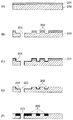
図1は本実施形態を説明するための工程図である。図1中、1,2は絶縁層(絶縁基材)、1aは第一電気回路、3は樹脂皮膜、4は回路溝、5は貫通孔、6はメッキ触媒、7は無電解メッキ膜、である。また、第一電気回路1aの表面の所定の位置には、略円錐状の導体バンプ(導体柱)1bが形成されている。
[First Embodiment]
FIG. 1 is a process diagram for explaining the present embodiment. In FIG. 1, 1 and 2 are insulating layers (insulating base materials), 1a is a first electric circuit, 3 is a resin film, 4 is a circuit groove, 5 is a through hole, 6 is a plating catalyst, 7 is an electroless plating film, It is. A substantially conical conductor bump (conductor pillar) 1b is formed at a predetermined position on the surface of the first
本実施形態の製造方法においては、はじめに、図1(A)に示すように、絶縁基材1表面に形成された第一電気回路1aと絶縁基材2とを重ね合わせ、第一電気回路1aの所定位置に突設された導体バンプ1bを埋設させるように積層する。それにより、図1(B)に示すように、積層一体化された導体柱含有回路基板9が形成される。このとき、第一電気回路1aの表面に突設された導体バンプ1bは絶縁基材2に侵入することにより埋設されている。
In the manufacturing method of the present embodiment, first, as shown in FIG. 1 (A), the first
絶縁基材としては、多層配線基板の製造に用いられうる各種有機基板が用いられる。有機基板の具体例としては、エポキシ樹脂シート、アクリル樹脂シート、ポリカーボネート樹脂シート、ポリイミド樹脂シート等が特に限定なく用いられうる。また、上記樹脂シートの他、繊維基板に熱硬化性樹脂が含浸されてなるプリプレグも好ましく用いられうる。絶縁基材2の厚みは特に限定されないが、例えば、10〜200μm、さらには20〜100μm程度であることが好ましい。
As the insulating base material, various organic substrates that can be used for manufacturing a multilayer wiring board are used. As specific examples of the organic substrate, an epoxy resin sheet, an acrylic resin sheet, a polycarbonate resin sheet, a polyimide resin sheet, and the like can be used without any particular limitation. In addition to the resin sheet, a prepreg obtained by impregnating a fiber substrate with a thermosetting resin can also be preferably used. Although the thickness of the insulating
また、導体柱含有回路基板9の形成においては、絶縁層1の第一電気回路1aが形成された側の表面に、樹脂溶液を塗布した後、硬化させることにより絶縁層2を形成してもよい。このような方法に用いられる樹脂溶液としては、従来から多層配線基板の製造に用いられているような、エポキシ樹脂、ポリフェニレンエーテル樹脂、アクリル樹脂、ポリイミド樹脂等の樹脂溶液が特に限定なく用いられうる。
Further, in forming the conductive pillar-containing circuit board 9, the insulating
本実施形態においては、第一電気回路1aは、絶縁基材1表面に形成されている。そして、第一電気回路1aの表面の所定の位置には導体バンプ1bが突設されている。第一電気回路1aは、サブトラクティブ法、アディティブ法等の従来から知られた回路形成方法により形成されうる。
In the present embodiment, the first
導体バンプ1bは、第一電気回路1aの表面に、導電性ペーストをスクリーン印刷することにより形成されうる。具体的には、スクリーン印刷により、例えば、銀ペースト等の導電性ペーストを第一電気回路1aの表面の所定の位置に印刷する。なお、一回の印刷で所望の高さが得られない場合には、スクリーン印刷を複数回繰り返して、導電性ペーストを高さ方向に継ぎ足してもよい。そして、所定の位置に導電性ペーストを載置した後、半硬化状態で頂部が尖った円錐状などの形状に成形し、さらに硬化させることにより導体バンプが形成される。また、半硬化状態で成形する代わりに、導電性ペーストを所定の位置に載置した後、硬化させた後、エッチングプロセスを用いて所定の形状に成形してもよい。また、別の方法としては、比較的厚膜の金属箔をフォトレジスト法を用いてエッチングすることにより形成したり、さらには、メッキプロセスを用いて形成してもよい。
The
導体バンプ1bの形状、大きさ、間隔等は特に限定されない。具体的には、例えば、略円錐状であって、高さが5〜200μm程度、底面の直径が10〜500μm程度のようなものが挙げられる。
The shape, size, interval, etc. of the
第一電気回路1aの表面に絶縁層2を形成するときの導体バンプ1bの埋設の形態は例えば、図2(A)に示すように、絶縁基材2に導体バンプ1bの頭部が露出せずに完全に埋没しているような形態や、図2(B)に示すように、絶縁基材2に導体バンプ1bが貫通するように突き刺され、導体バンプ1bの頂部のみが露出するような形態など、特に限定されない。
As shown in FIG. 2A, for example, the
絶縁層2の形成は、例えば、絶縁基材2を絶縁層1表面に形成された第一電気回路1aに重ね合わせ、加熱プレスすることにより行われうる。絶縁基材2としてプリプレグを用いる場合には、この加熱プレスにより硬化させてもよい。
The insulating
次に、図1(C)に示すように、導体柱含有回路基板9の主面(導体バンプ1bの突設側に対向する絶縁層2の表面)に樹脂皮膜3を形成する(皮膜形成工程)。
Next, as shown in FIG. 1C, a resin film 3 is formed on the main surface of the conductor column containing circuit board 9 (the surface of the insulating
樹脂皮膜3は、絶縁層2の表面に液状材料を塗布した後、乾燥させたり、絶縁層2の表面に、予め形成された樹脂フィルムを貼り合せたりすることにより形成される。
The resin film 3 is formed by applying a liquid material to the surface of the insulating
樹脂皮膜3は、所定の液体で膨潤または溶解させることにより、絶縁層2の表面から容易に除去しうるような樹脂皮膜が好ましく用いられうる。具体的には、例えば、有機溶剤やアルカリ溶液により容易に溶解しうる可溶型樹脂からなる皮膜や、所定の溶媒で膨潤しうる膨潤性樹脂からなる皮膜(本明細書においては、膨潤性樹脂皮膜ともいう)が挙げられる。これらの中では、正確な除去が容易である点から膨潤性樹脂皮膜が特に好ましい。
As the resin film 3, a resin film that can be easily removed from the surface of the insulating
膨潤性樹脂皮膜としては、膨潤液に対する膨潤度が50%以上、さらには100%以上で、1000%以下であるような膨潤度の樹脂皮膜が好ましく用いられうる。前記膨潤度が低すぎる場合には、膨潤性樹脂皮膜が剥離しにくくなる傾向があり、高すぎる場合には、皮膜強度が低下することにより剥離する際に破れる等して剥離が困難になる傾向がある。このような膨潤性樹脂は、絶縁層2の表面にエラストマーのサスペンジョン又はエマルジョンを塗布した後、乾燥することや、支持基板にそれらを塗布した後、乾燥することにより形成される皮膜を絶縁層2の表面に転写することにより形成することができる。
As the swellable resin film, a resin film having a degree of swelling with respect to the swelling liquid of 50% or more, more preferably 100% or more and 1000% or less can be preferably used. When the degree of swelling is too low, the swellable resin film tends to be difficult to peel, and when it is too high, the film strength is reduced, and the film tends to be difficult to peel due to tearing when peeling. There is. Such a swellable resin has a coating formed by applying an elastomer suspension or emulsion on the surface of the insulating
このようなエラストマーの具体例としては、スチレン−ブタジエン系共重合体等のジエン系エラストマー、アクリル酸エステル系共重合体等のアクリル系エラストマー、及びポリエステル系エラストマー等が挙げられる。このようなエラストマーによれば、サスペンジョン又はエマルジョンとして分散されたエラストマー樹脂粒子の架橋度またはゲル化度等を調整することにより所望の膨潤度の膨潤性樹脂皮膜を容易に形成することができる。 Specific examples of such elastomers include diene elastomers such as styrene-butadiene copolymers, acrylic elastomers such as acrylic ester copolymers, and polyester elastomers. According to such an elastomer, a swellable resin film having a desired swelling degree can be easily formed by adjusting the degree of crosslinking or gelation of the elastomer resin particles dispersed as a suspension or emulsion.
塗布する方法は特に限定されず、従来から知られたスピンコート法やバーコーター法等が特に限定なく用いられうる。 The coating method is not particularly limited, and conventionally known spin coating methods, bar coater methods, and the like can be used without particular limitation.
樹脂皮膜3の厚みとしては、10μm以下、さらには5μm以下であり、0.1μm以上、さらには1μm以上であることが好ましい。樹脂皮膜3の厚みが厚すぎる場合には、微細な回路パターンをレーザー加工により形成する際に精度が低下する傾向があり、前記厚みが薄すぎる場合は、均一な膜厚の樹脂皮膜を形成しにくくなる傾向がある。 The thickness of the resin film 3 is 10 μm or less, further 5 μm or less, preferably 0.1 μm or more, and more preferably 1 μm or more. If the thickness of the resin film 3 is too thick, the accuracy tends to decrease when a fine circuit pattern is formed by laser processing. If the thickness is too thin, a resin film having a uniform film thickness is formed. There is a tendency to become difficult.
次に、図1(D)に示すように、樹脂皮膜3の外表面側からレーザー加工することにより、少なくとも前記樹脂皮膜の厚み分以上の深さの回路溝4を形成する(回路溝形成工程)。このようにレーザー加工を用いることにより、配線幅20μm以下のような微細な回路溝も容易に形成することができる。このような微細な金属配線を形成することにより、高精度の加工が要求されるアンテナ回路等を容易に形成することができる。また、レーザー加工によれば、レーザーの強度を変化させることにより、切削深さ等を自由に調整することができる。また、レーザー加工によれば、絶縁層2の電気回路を形成したい部分の樹脂皮膜のみを選択的に除去することができる。これにより、後述する触媒付着工程と皮膜除去工程とを経て、絶縁層2の電気回路を形成したい部分のみにメッキ触媒を残留させることができるために、高精度な輪郭を維持した第二電気回路を形成することができる。
Next, as shown in FIG. 1 (D), laser processing is performed from the outer surface side of the resin film 3 to form a
そして、図1(D)に示すように、樹脂皮膜3の外表面側からレーザー加工することにより、導体バンプ1bを露出させる(導体柱露出工程)。このとき、導体バンプ1bを露出させることにより、絶縁層2を貫通する貫通孔5が形成される。導体バンプ1bの露出は表面のスミアを充分に除去するために、図3に示すように、その頂部を除去して、導体バンプ1b自身を掘り込んだような状態になるように露出させることが好ましい。導体バンプ1bは、第一電気回路1aに比べて充分な厚みを有するために、高いレーザー強度で照射しても、孔ができるようなことがない。従って、第一電気回路1aの表面に突設された導体バンプ1bを掘り込むように高い強度でレーザー加工したとしても、第一電気回路1a自身は損傷されない。そして、このように導体バンプ1bを露出させることにより、導体バンプ1b表面のスミアを完全に除去することができる。従って、デスミア処理しなくても新たに形成される第二電気回路の金属配線と導体バンプとの間で充分な層間接続を維持することができる。すなわち、レーザー加工により導体バンプ1bを露出させた後、後述するメッキ処理を施すことにより、露出した導体バンプ1bと新たに形成される第二電気回路とをメッキ膜により層間接続することができる。
And as shown in FIG.1 (D), the
次に、図1(E)に示すように、レーザー加工により露出した導体バンプ1b,回路溝4及び樹脂皮膜3の外表面全体にメッキ触媒またはその前駆体を付着させる(触媒付着工程)。
Next, as shown in FIG. 1E, a plating catalyst or a precursor thereof is attached to the entire outer surfaces of the conductor bumps 1b, the
メッキ触媒6は、後述するメッキ処理工程において、無電解メッキ膜を充分且つ効果的に成長形成させるために付与される触媒またはその前駆体であり、無電解メッキ用の触媒として知られたものであれば特に限定なく用いられうる。その具体例としては、例えば、金属パラジウム(Pd)、白金(Pt)、銀(Ag)等、または、これらを生成させるような前駆体等が挙げられる。
The
メッキ触媒6を付着させる方法としては、例えば、次のような方法が挙げられる。はじめに、絶縁層2の表面に付着している油分等を除去するために、界面活性剤溶液中で所定の時間湯洗する。次に、濃度0.1%程度の塩化第一錫水溶液等に浸漬して塩化第一錫を吸着させた後、濃度0.01%程度の塩化パラジウム水溶液等にさらに浸漬することにより塩化パラジウムを吸着させる。そして、レーザー加工された部分の表面、及びレーザー加工されていない樹脂皮膜3の表面全体において、吸着した塩化第一錫と塩化パラジウムとの間で酸化還元反応(SnCl2+PdCl2→SnCl4+Pd↓)させることにより金属パラジウムを形成させる。
Examples of the method for attaching the
このような触媒付着処理により、図1(E)に示すように、レーザー加工された部分の表面、及びレーザー加工されていない樹脂皮膜3の表面全体にメッキ触媒6を付着させることができる。
By such a catalyst adhesion treatment, as shown in FIG. 1E, the
次に、図1(F)に示すように、樹脂皮膜3を所定の液体で膨潤または溶解させることにより除去する(皮膜除去工程)。この工程によれば、レーザー加工により形成された回路溝4及び露出した導体バンプ1bの表面のみにメッキ触媒6を残留させ、それ以外の部分(樹脂皮膜3の表面)に付着されたメッキ触媒6を除去することができる。
Next, as shown in FIG. 1 (F), the resin film 3 is removed by swelling or dissolving with a predetermined liquid (film removal step). According to this step, the
皮膜除去工程において、樹脂皮膜3を除去する方法としては、アルカリ溶液等の所定の液に所定の時間浸漬することにより、樹脂皮膜3を溶解除去する方法や又は樹脂皮膜3を膨潤させて剥離する方法が挙げられる。アルカリ溶液としては、所定の濃度のアルカリ水溶液、例えば、1〜10%程度の濃度の水酸化ナトリウム水溶液等が用いられうる。また、この際、除去効率を高めるために、浸漬中に超音波照射することが好ましい。なお、膨潤させて剥離するときには、必要に応じて軽い力で引き剥がしてもよい。 In the film removal step, the resin film 3 can be removed by immersing it in a predetermined liquid such as an alkaline solution for a predetermined time to dissolve and remove the resin film 3 or swell and peel the resin film 3. A method is mentioned. As the alkaline solution, an alkaline aqueous solution having a predetermined concentration, for example, a sodium hydroxide aqueous solution having a concentration of about 1 to 10% can be used. At this time, in order to increase the removal efficiency, it is preferable to irradiate with ultrasonic waves during the immersion. In addition, when it swells and peels, you may peel off with a light force as needed.
次に、図1(G)に示すように、皮膜除去工程の後に、メッキ触媒6が残留する部位に、無電解メッキ膜を形成する(メッキ処理工程)。この工程により、第二電気回路を形成したい部分のみに無電解メッキ膜を析出させることができる。また、この工程により、新たに形成される上層の第二電気回路8と下層の第一電気回路1aとが導体バンプ1b及び無電解メッキ膜7を介して層間接続される。
Next, as shown in FIG. 1G, after the film removal step, an electroless plating film is formed in a portion where the
無電解メッキ膜の形成方法としては、皮膜除去工程後の導体柱含有回路基板9を無電解めっき液に浸漬することにより、メッキ触媒6が付着された部分のみに無電解メッキ膜7を析出させる方法が用いられうる。
The electroless plating film is formed by immersing the conductive column-containing circuit board 9 after the film removal step in an electroless plating solution so that the
無電解メッキに用いられる金属としては、Cu(銅)、Ni(ニッケル)、Co(コバルト)、Al(アルミニウム)等が挙げられる。これらの中では、Cuを主成分とするメッキが導電性に優れている点から好ましく、また、Niを含む場合には耐食性や、はんだ等との密着性に優れている点等から好ましい。 Examples of the metal used for electroless plating include Cu (copper), Ni (nickel), Co (cobalt), and Al (aluminum). Among these, plating containing Cu as a main component is preferable from the viewpoint of excellent conductivity, and when Ni is contained, it is preferable from the viewpoint of excellent corrosion resistance and adhesion to solder or the like.
無電解メッキ膜7の膜厚は、特に限定されないが、0.1〜10μm、さらには1〜5μm程度であることが好ましい。
The film thickness of the
このようなメッキ処理工程により、絶縁層2表面のレーザー加工された部分のみに無電解メッキ膜7を析出させることができる。これにより絶縁層2表面に第二電気回路8が形成されるとともに、形成された第二電気回路8と第一電気回路1aとが導体バンプ1bにより層間接続される。
By such a plating process, the
このような工程を経て、図1(G)に示すような絶縁層2の表面に第二電気回路8を有する多層配線基板10が形成される。多層配線基板10においては、上層の第2電気回路8は導体バンプ1b及び無電解メッキ膜7を介して下層の第1電気回路1aと導通化されている。
Through such steps, the
なお、本実施形態の製造方法を用いれば、レーザー加工による除去深さを調整することにより、図4に示すように、絶縁層2の深い部分に形成される第二電気回路8aや、8aと8bのように、互いに深さの異なる位置に第二電気回路を形成したりすることもできる。また、8cに示すように、形成される溝を深く形成して厚膜にメッキ膜を形成することにより、断面積が大きい金属配線を容易に形成することができる。この場合には、金属配線の電気容量を増加させることができるとともに、金属配線の強度を向上させることができる点から好ましい。
In addition, if the manufacturing method of this embodiment is used, as shown in FIG. 4, by adjusting the removal depth by laser processing, the second
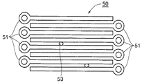
上記多層配線基板の製造方法においては、樹脂皮膜3に蛍光性物質を含有させることにより、上述した皮膜除去工程の後、検査対象面に紫外光や近紫外 光を照射することによる蛍光性物質からの発光を用いて皮膜除去不良を検査することができる。本実施形態の多層配線基板の製造方法においては、配線幅及び配線間隔が極端に小さい金属配線を形成することができる。このような場合においては、図5の回路50の上面拡大図における樹脂皮膜の残渣53として示したように、隣接する金属配線51間の樹脂皮膜が完全に除去されずに残留することが懸念される。金属配線間に樹脂皮膜が残留した場合には、その部分にメッキ膜が形成されてしまい、マイグレーションや短絡の原因になりうる。このような場合、樹脂皮膜3に蛍光性物質を含有させ、皮膜除去工程の後、皮膜除去面に所定の発光源を照射して皮膜が残留している部分のみを蛍光性物質により発光させることにより、皮膜除去不良の有無や皮膜除去不良の箇所を検査することができる。
In the manufacturing method of the multilayer wiring board, by adding a fluorescent substance to the resin film 3, the fluorescent substance is irradiated by irradiating the surface to be inspected with ultraviolet light or near ultraviolet light after the film removing step described above. The film removal failure can be inspected using the luminescence. In the method for manufacturing a multilayer wiring board according to the present embodiment, a metal wiring having an extremely small wiring width and wiring interval can be formed. In such a case, as shown as a
本検査工程に用いられる樹脂皮膜に含有させうる蛍光性物質は、所定の光源により光を照射することにより発光特性を示すものであればとくに限定されない。その具体例としては、例えば、Fluoresceine、Eosine、Pyronine G等が挙げられる。 The fluorescent substance that can be contained in the resin film used in this inspection process is not particularly limited as long as it exhibits light emission characteristics when irradiated with light from a predetermined light source. Specific examples thereof include Fluoresceine, Eosine, Pyroline G, and the like.
本検査工程により蛍光性物質からの発光が検出された部分は、樹脂皮膜3が残留する部分である。従って、発光が検出された部分を除去することにより、その部分にメッキ膜が形成されることを抑制できる。これにより、マイグレーションや短絡の発生を未然に抑制することができる。 The portion where the light emission from the fluorescent substance is detected by this inspection process is the portion where the resin film 3 remains. Therefore, by removing the portion where light emission is detected, it is possible to suppress the formation of a plating film on that portion. Thereby, generation | occurrence | production of a migration or a short circuit can be suppressed beforehand.
なお、本実施形態においては、上述のように、絶縁基材1表面に形成された第一電気回路1aを用いたが、電気回路を用いる代わりに、回路形成されていない金属箔を用いてもよい。この場合には所定の部分に導体バンプが形成された金属箔シートが用いることができる。そして、メッキ処理工程後に、サブトラクティブ法により積層一体化された金属箔をエッチングして電気回路を形成してもよい。
In the present embodiment, as described above, the first
以上説明した多層配線基板の製造方法によれば、ビルドアップ法により電気回路を積層して多層配線基板を製造するに際して、下層の第一電気回路に形成されている導体バンプをレーザー加工することにより露出させて無電解メッキ膜を形成することにより、新たに形成される上層の第二電気回路と予め形成されている下層の第一電気回路との層間接続を容易に実現できる。また、新たに形成される第二電気回路は、金属配線を形成したい部分のみにメッキ触媒を付着させて形成されるために、形状精度の高い電気回路が得られる。これにより、形状精度の高い電気回路が形成された多層配線基板を提供することができる。このような多層配線基板の製造方法を用いることにより、配線幅及び配線間隔が狭いICサブストレート、携帯電話用プリント配線板、立体配線基板等の用途に用いられる多層配線基板を製造することができる。 According to the method for manufacturing a multilayer wiring board described above, when a multilayer wiring board is manufactured by stacking electrical circuits by the build-up method, the conductor bumps formed on the lower first electrical circuit are laser processed. By exposing and forming the electroless plating film, interlayer connection between the newly formed upper second electric circuit and the lower first electric circuit formed in advance can be easily realized. In addition, since the newly formed second electric circuit is formed by attaching the plating catalyst only to the portion where the metal wiring is to be formed, an electric circuit with high shape accuracy can be obtained. Thereby, it is possible to provide a multilayer wiring board on which an electric circuit with high shape accuracy is formed. By using such a multilayer wiring board manufacturing method, it is possible to manufacture a multilayer wiring board used for applications such as an IC substrate having a narrow wiring width and wiring interval, a printed wiring board for a mobile phone, and a three-dimensional wiring board. .
[第2実施形態]
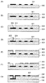
第2実施形態では、第一電気回路の所定位置に突設された導体柱を埋設させるように絶縁層が形成されてなる、導体柱含有回路基板の他の製造方法について説明する。なお、導体柱含有回路基板の製造以外の各工程は、第1実施形態と同様の工程が用いられうるので、詳しい説明は省略する。
[Second Embodiment]
2nd Embodiment demonstrates the other manufacturing method of a conductor pillar containing circuit board by which an insulating layer is formed so that the conductor pillar protruded in the predetermined position of the 1st electric circuit may be embedded. In addition, since each process other than manufacture of a conductor pillar containing circuit board can use the process similar to 1st Embodiment, detailed description is abbreviate | omitted.
第2実施形態における導体柱含有回路基板の製造方法について、図6を参照して説明する。 The manufacturing method of the conductor pillar containing circuit board in 2nd Embodiment is demonstrated with reference to FIG.
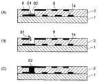
図6中、1,2は絶縁層(絶縁基材)、1aは第一電気回路、60はレーザー加工された穴、61はスミア、62は導体柱である。 In FIG. 6, 1 and 2 are insulating layers (insulating base materials), 1a is a first electric circuit, 60 is a laser processed hole, 61 is a smear, and 62 is a conductor post.
本実施形態の製造方法においては、はじめに、図6(A)及び図6(B)に示すように、第一電気回路1aが形成されている絶縁層1の表面に絶縁層2を形成する。そして、図6(C)に示すように、絶縁層2の第一電気回路1aとの張り合わせ面に対する反対面から、絶縁層にレーザー加工等により穴あけ加工することにより、第一電気回路1aの表面を露出させる。このとき、レーザー加工により形成された穴60の底部における第一電気回路1aの表面には、図6(C)に示すように、樹脂残渣であるスミア61が残る。穴60の底部に残ったスミア61は導通不良の原因となる。このためスミア61は、デスミア処理により、図6(D)に示すように除去することが好ましい。なお、デスミア処理は、過マンガン酸溶液等に浸漬することによりスミア61を溶解除去するための公知の方法が特に限定なく用いられる。
In the manufacturing method of the present embodiment, first, as shown in FIGS. 6A and 6B, the insulating
そして、デスミア処理した後、露出させた第一電気回路1aの表面から電解メッキまたは無電解メッキによりメッキを成長させることにより、図6(E)に示すように、第一電気回路1aの表面に導体柱62が突設される。なお、電解メッキを施す場合には、第一電気回路1aが電極として機能し、無電解メッキを施す場合には第一電気回路1aの表面がメッキ核として機能する。
Then, after the desmear treatment, the plating is grown from the exposed surface of the first
第1実施形態で用いた導体柱含有回路基板9の代わりに、上述した導体柱含有回路基板69を用いる以外は、第1実施形態で説明したのと同様の各工程を用いることにより、多層配線基板が得られる。すなわち、導体柱含有回路基板69の表面に樹脂皮膜3を形成する(皮膜形成工程)。そして、樹脂皮膜3の外表面側からのレーザー加工することにより、少なくとも前記樹脂皮膜の厚み分以上の深さの回路溝4を形成する(回路溝形成工程)。そして、樹脂皮膜3の外表面側からレーザー加工することにより、導体柱62を露出させる(導体柱露出工程)。そして、レーザー加工により露出した導体柱62,回路溝4及び樹脂皮膜3の外表面全体にメッキ触媒またはその前駆体を付着させる(触媒付着工程)。そして、樹脂皮膜3を所定の液体で膨潤または溶解させることにより除去する(皮膜除去工程)。そして、皮膜除去工程の後に、メッキ触媒6が残留する部位に、無電解メッキ膜を形成する(メッキ処理工程)。このような工程を経て、絶縁層2の表面に第二電気回路8を有する多層配線基板が形成される。多層配線基板においては、上層の第2電気回路8は導体柱62及び無電解メッキ膜7を介して下層の第1電気回路1aと導通化されている。
By using the same steps as those described in the first embodiment except that the above-described conductor pillar-containing
このような方法によれば、樹脂皮膜を形成させる前に第一電気回路表面にデスミア処理を施し、その後、電解メッキまたは無電解メッキにより層間接続部になる導電柱を形成することができる。従って、デスミア処理により樹脂皮膜等が生じるおそれがない。また、露出させた第一電気回路を電極として給電することにより、電解メッキによりメッキを成長形成させた場合には、より効率的に導電柱を形成することができる。また、第一電気回路に給電することが困難な場合には、露出した前記電気回路表面をメッキ核として、無電解メッキによりメッキ膜を成長形成させることもできる。 According to such a method, it is possible to perform desmear treatment on the surface of the first electric circuit before forming the resin film, and then form conductive columns to be interlayer connection portions by electrolytic plating or electroless plating. Therefore, there is no possibility that a resin film or the like is generated by the desmear treatment. In addition, when the exposed first electric circuit is fed as an electrode, the conductive pillar can be formed more efficiently when the plating is grown by electrolytic plating. Further, when it is difficult to supply power to the first electric circuit, a plating film can be grown and formed by electroless plating using the exposed surface of the electric circuit as a plating nucleus.
[第3実施形態]
第3実施形態では、第1実施形態及び第2実施形態で説明したように、樹脂皮膜3を形成する前に形成された導電柱を用いる代わりに、樹脂皮膜を剥離して第二電気回路を形成した後に、層間接続部となる導体柱を形成する方法について説明する。なお、第1実施形態及び第2実施形態で説明したと同様の工程については、詳しい説明は省略する。
[Third Embodiment]
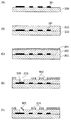
In the third embodiment, as described in the first embodiment and the second embodiment, instead of using the conductive pillar formed before the resin film 3 is formed, the resin film is peeled and the second electric circuit is formed. A method of forming a conductor post that will be an interlayer connection after the formation will be described. Detailed description of the same steps as those described in the first embodiment and the second embodiment will be omitted.
本実施形態の製造方法においては、はじめに、図7(A)に示すように、絶縁基材1表面に形成された第一電気回路1aに絶縁層2を積層する。それにより、図7(B)に示すように、積層一体化された導体柱含有回路基板79が形成される。
In the manufacturing method of the present embodiment, first, as shown in FIG. 7A, the insulating
次に、図7(C)に示すように、絶縁層2の表面に樹脂皮膜3を形成する(皮膜形成工程)。次に、図7(D)に示すように、樹脂皮膜3の外表面側からのレーザー加工することにより、少なくとも樹脂皮膜3の厚み分以上の深さの回路溝4を形成する(回路溝形成工程)。
Next, as shown in FIG. 7C, a resin film 3 is formed on the surface of the insulating layer 2 (film formation process). Next, as shown in FIG. 7D, the
次に、図7(E)に示すように、レーザー加工により形成された回路溝4及び樹脂皮膜3の外表面全体にメッキ触媒6を付着させる(触媒付着工程)。このような触媒付着処理により、レーザー加工された回路溝4の表面、及びレーザー加工されていない樹脂皮膜3の表面全体にメッキ触媒6を付着させることができる。
Next, as shown in FIG. 7E, a
次に、図7(F)に示すように、樹脂皮膜3を所定の液体で膨潤または溶解させることにより除去する(皮膜除去工程)。この工程によれば、レーザー加工により形成された回路溝4の表面のみにメッキ触媒6を残留させ、それ以外の樹脂皮膜3の表面に付着されたメッキ触媒6を除去することができる。
Next, as shown in FIG. 7F, the resin film 3 is removed by swelling or dissolving with a predetermined liquid (film removal step). According to this step, it is possible to leave the
次に、図7(G)に示すように、皮膜除去工程の後に、メッキ触媒6が残留する部位に、無電解メッキ膜を形成する(メッキ処理工程)。この工程により、第二電気回路8を形成したい部分のみに無電解メッキ膜を析出させることができる。
Next, as shown in FIG. 7G, after the film removal step, an electroless plating film is formed in a portion where the
次に、図8(A)に示すように、第二電気回路8の層間接続を形成したい部分において穴あけ加工することにより、第一電気回路1a表面を露出させる(穴あけ工程)。このように第二電気回路8の形成後に、第一電気回路との穴あけ加工することにより所望の部分に層間接続部を形成することができる。このとき、レーザー加工により形成された穴80の底部における第一電気回路1aの表面には、図8(A)に示すように、樹脂残渣であるスミア81が残る。穴80の底部に残ったスミア81は導通不良の原因となる。このためスミア81は、デスミア処理により、図8(B)に示すように除去することが好ましい。
Next, as shown in FIG. 8 (A), the surface of the first
そして、デスミア処理した後、露出させた第一電気回路1aの表面から電解メッキまたは無電解メッキによりメッキを成長させることにより、図8(C)に示すように、第一電気回路1aの表面に導体柱82が突設される。なお、電解メッキを施す場合には、第一電気回路1aが電極として機能し、無電解メッキを施す場合には第一電気回路1aの表面がメッキ核として機能する。
Then, after the desmear treatment, the plating is grown from the exposed surface of the first
このような方法によれば、樹脂皮膜3を剥離して第二電気回路8を形成した後に、層間接続部となる導体柱82を形成するために、穴あけ加工後にデスミア処理しても第二電気回路8の形成に影響しない。その結果、ビルドアップ法により、配線幅や配線間隔が狭い第二電気回路を積層する場合でも、短絡やマイグレーションの発生が抑制された第二電気回路が形成される。
According to such a method, after the resin film 3 is peeled to form the second
以下、本発明を実施例により、さらに詳しく説明する。なお、本発明の範囲は、実施例により何ら限定されるものではない。 Hereinafter, the present invention will be described in more detail with reference to examples. The scope of the present invention is not limited by the examples.
表面に金属配線(厚み18μm)が形成された回路基板を厚み100μmのプリプレグに重ね合わせる。なお、前記金属配線の表面には、所定の位置に高さ50μm、底面の直径200μmの円錐状導体バンプが形成されている。この導体バンプは、導電性ペーストにより形成されたものである。そして、この重ね合わせ体を導体バンプがプリプレグに侵入するように加熱加圧成形することにより、重ね合わせ体が積層一体化された積層体が得られる。 A circuit board having a metal wiring (thickness: 18 μm) formed on the surface is overlaid on a prepreg having a thickness of 100 μm. A conical conductor bump having a height of 50 μm and a bottom surface diameter of 200 μm is formed on the surface of the metal wiring at a predetermined position. This conductor bump is formed of a conductive paste. And this laminated body is heat-press-molded so that a conductor bump may penetrate | invade a prepreg, and the laminated body by which the laminated body was laminated and integrated is obtained.
次に、得られた積層体のプリプレグ側表面にスピンコート法を用いて、スチレン−ブタジエン共重合体(SBR)のメチルエチルケトン(MEK)サスペンジョン(日本ゼオン(株)製、粒子径200nm、固形分15%)を塗布し、80℃で30分間乾燥することにより、2μm厚の樹脂皮膜を形成する。 Next, a styrene-butadiene copolymer (SBR) methyl ethyl ketone (MEK) suspension (manufactured by Nippon Zeon Co., Ltd., particle size: 200 nm, solid content: 15) is applied to the prepreg side surface of the obtained laminate using a spin coating method. %) And dried at 80 ° C. for 30 minutes to form a 2 μm thick resin film.
そして、樹脂皮膜が形成された積層体に対して、レーザー加工により所定の位置に幅20μm、深さ30μmの略長方形断面の溝形成を行う。また、導体バンプが形成されている部分に向けて、導体バンプを掘り込んで露出させるように孔形成を行う。なお、レーザー加工にはUV−YAGレーザーを備えたESI社製のMODEL5330を用いる。 Then, a groove having a substantially rectangular cross section with a width of 20 μm and a depth of 30 μm is formed at a predetermined position by laser processing on the laminate on which the resin film is formed. Further, holes are formed so as to dig and expose the conductor bumps toward the portion where the conductor bumps are formed. For laser processing, MODEL 5330 manufactured by ESI equipped with a UV-YAG laser is used.
次に、レーザー加工された積層体をクリーナーコンディショナー(C/N3320)中に浸漬した後、水洗する。そして、付着されるスズ−パラジウムコロイドの分解を抑制するために、PD404(シプレイ・ファーイースト(株)製)を用いてプリディップ工程を行う。そして、キャタリスト液(CAT44、シプレイ・ファーイースト(株)製)に浸漬し、無電解銅メッキの核となるパラジウムをスズ−パラジウムコロイドの状態で樹脂皮膜が形成された積層体に吸着させる。 Next, the laser-processed laminate is immersed in a cleaner conditioner (C / N 3320) and then washed with water. And in order to suppress decomposition | disassembly of the tin- palladium colloid adhering, a pre-dip process is performed using PD404 (made by Shipley Far East Co., Ltd.). Then, it is immersed in a catalyst liquid (CAT44, manufactured by Shipley Far East Co., Ltd.), and palladium serving as the core of electroless copper plating is adsorbed to the laminate on which the resin film is formed in a tin-palladium colloid state.
そして、スズ−パラジウムコロイドが吸着された積層体を、5%水酸化ナトリウム水溶液中に超音波処理しながら10分間浸漬することにより、表面のSBR皮膜を膨潤させることにより、樹脂皮膜を剥離させる。 The laminate on which the tin-palladium colloid is adsorbed is immersed in a 5% aqueous sodium hydroxide solution for 10 minutes while being ultrasonically treated to swell the SBR film on the surface, thereby peeling the resin film.
次に、積層体表面に紫外光を照射する。このとき、紫外光の照射により部分的に蛍光発光が認められる。蛍光部分が認められた部分は、布でラビングすることにより除去する。 Next, the surface of the laminate is irradiated with ultraviolet light. At this time, fluorescence emission is partially recognized by irradiation with ultraviolet light. The part where the fluorescent part is recognized is removed by rubbing with a cloth.
次に、積層体をアクセレータ薬液(ACC19E、シプレイ・ファーイースト(株)製)に浸漬することにより、パラジウム核を発生させる。そして、積層体を無電解メッキ液(CM328A,CM328L、CM328C、シプレイ・ファーイースト(株)製)に浸漬させて無電解銅メッキ処理を行う。これにより、厚み5μmの無電解銅メッキ膜が析出する。上述のような無電解メッキ処理された積層体表面をSEM(走査型顕微鏡)により観察することにより、レーザー加工された溝部分には、無電解メッキ膜により形成された金属配線が高精度に形成されており、また、導体バンプの表面と溝部分とが無電解メッキ膜により導通化されていることが確認できる。 Next, palladium nuclei are generated by immersing the laminate in an accelerator chemical (ACC19E, manufactured by Shipley Far East Co., Ltd.). Then, the laminate is immersed in an electroless plating solution (CM328A, CM328L, CM328C, manufactured by Shipley Far East Co., Ltd.) to perform an electroless copper plating process. Thereby, an electroless copper plating film having a thickness of 5 μm is deposited. By observing the surface of the laminate subjected to electroless plating as described above with an SEM (scanning microscope), the metal wiring formed of the electroless plating film is formed with high precision in the laser-processed groove portion. Further, it can be confirmed that the surface of the conductor bump and the groove portion are made conductive by the electroless plating film.
なお、膨潤性樹脂皮膜の膨潤度は、以下のように測定する。 The degree of swelling of the swellable resin film is measured as follows.
離型紙上に、絶縁基材上に膨潤性樹脂皮膜を形成するために塗布したSBRサスペンジョンを塗布し、80℃で30分間乾燥することにより、エポキシ樹脂基板に形成した厚みと同様の厚みである、2μm厚の皮膜を形成する。そして、形成された皮膜を強制的に剥離したものを試料とする。そして、得られた試料0.02g程度を秤量する。このときの試料重量を膨潤前重量m’とする。そして、秤量された試料を20±2℃の水酸化ナトリウム5%水溶液10ml中に15分間浸漬する。そして、遠心分離器を用いて1000Gで約10分間遠心分離処理を行い、試料に付着した水分等を除去する。そして、遠心分離後の膨潤した試料の重量を測定し、膨潤後重量mとする。得られた、膨潤前重量m’及び膨潤後重量mから、
「膨潤度SW=(m−m’)/m’×100(%)」の式から、膨潤度を算出する。なお、その他の条件は、JIS L1015 8.27(アルカリ膨潤度の測定方法)に準じて行う。このとき、得られる膨潤度は約750%である。
On the release paper, the SBR suspension applied to form the swellable resin film on the insulating base material is applied and dried at 80 ° C. for 30 minutes, so that the thickness is the same as the thickness formed on the epoxy resin substrate. A film having a thickness of 2 μm is formed. Then, a sample obtained by forcibly peeling the formed film is used as a sample. Then, about 0.02 g of the obtained sample is weighed. The weight of the sample at this time is defined as a weight m ′ before swelling. Then, the weighed sample is immersed in 10 ml of 5% aqueous sodium hydroxide solution at 20 ± 2 ° C. for 15 minutes. Then, centrifugal separation is performed at 1000 G for about 10 minutes using a centrifuge to remove moisture and the like attached to the sample. Then, the weight of the swollen sample after centrifugation is measured, and the weight after swelling is defined as m. From the obtained weight m ′ before swelling and weight m after swelling,
The degree of swelling is calculated from the formula “swelling degree SW = (m−m ′) / m ′ × 100 (%)”. In addition, other conditions are performed according to JIS L1015 8.27 (measurement method of alkali swelling degree). At this time, the degree of swelling obtained is about 750%.
1,2,100,300 絶縁層(絶縁基材)
1a 第一電気回路
8,8a,8b,8c,51 第二電気回路
1b,62,82 導体柱(導体バンプ)
3 樹脂皮膜
4,202 回路溝
5,60,80,101,203,304 スルーホール(貫通孔)
6,102,204 メッキ触媒
7 無電解メッキ膜
9,69,79 導体柱含有回路基板
10 多層配線基板
50 回路
53 樹脂皮膜の残渣
61,81,305 スミア
103,306 フォトレジスト層
104 金属配線
105 余分なメッキ膜
110 フォトマスク
200,302 絶縁樹脂層
201 保護膜
205 導電層
1,2,100,300 Insulating layer (insulating base material)
1a First
3
6, 102, 204
Claims (15)
前記樹脂皮膜の外表面側からレーザー加工することにより、少なくとも前記樹脂皮膜の厚み分以上の深さの回路溝を形成する回路溝形成工程と、
前記樹脂皮膜の外表面側からレーザー加工することにより、前記導体柱を露出させる導体柱露出工程と、
前記露出した導体柱,前記回路溝表面及び前記樹脂皮膜の外表面全体にメッキ触媒を付着させる触媒付着工程と、
前記樹脂皮膜を除去する皮膜除去工程と、
前記皮膜除去工程の後に、前記メッキ触媒が残留する部位に無電解メッキ膜を形成させることにより、第二電気回路を形成するとともに前記導体柱により前記第一電気回路と前記第二電気回路との層間接続を形成するメッキ処理工程と、を備えることを特徴とする多層配線基板の製造方法。 A resin film is formed on the surface of the insulating layer on the protruding side of the conductor column of the conductor column-containing circuit board in which the insulating layer is formed so as to embed the conductor column protruding at a predetermined position of the first electric circuit. A film forming process;
A circuit groove forming step of forming a circuit groove having a depth equal to or greater than the thickness of the resin film by laser processing from the outer surface side of the resin film;
Conductor pillar exposing step of exposing the conductor pillar by laser processing from the outer surface side of the resin film,
A catalyst attaching step of attaching a plating catalyst to the exposed conductor pillar, the surface of the circuit groove and the entire outer surface of the resin film;
A film removing step for removing the resin film;
After the film removal step, an electroless plating film is formed on a portion where the plating catalyst remains, thereby forming a second electric circuit and the first electric circuit and the second electric circuit by the conductor column. And a plating process for forming an interlayer connection.
前記絶縁層表面に樹脂皮膜を形成する皮膜形成工程と、
前記樹脂皮膜の外表面側からレーザー加工することにより、少なくとも前記樹脂皮膜の厚み分以上の深さの回路溝を形成する回路溝形成工程と、
前記回路溝表面及び前記樹脂皮膜の外表面全体にメッキ触媒を付着させる触媒付着工程と、
前記樹脂皮膜を除去する皮膜除去工程と、
前記皮膜除去工程の後に、前記メッキ触媒が残留する部位に無電解メッキ膜を形成させることにより第二電気回路を形成するメッキ処理工程と、
前記第二電気回路の所定の部分において穴あけ加工することにより、前記第一電気回路を露出させる穴あけ工程と、
露出した前記第一電気回路の表面からメッキ膜を成長形成させることにより穴あけ加工された部分に導体柱を形成することにより前記第一電気回路と前記第二電気回路との層間接続部を形成する層間接続部形成工程と、を備えることを特徴とする多層配線基板の製造方法。 An insulating layer forming step of forming an insulating layer on the formation surface of the first electric circuit formed on the substrate;
A film forming step of forming a resin film on the surface of the insulating layer;
A circuit groove forming step of forming a circuit groove having a depth equal to or greater than the thickness of the resin film by laser processing from the outer surface side of the resin film;
A catalyst attaching step for attaching a plating catalyst to the entire surface of the circuit groove and the outer surface of the resin film;
A film removing step for removing the resin film;
A plating treatment step of forming a second electric circuit by forming an electroless plating film in a portion where the plating catalyst remains after the coating removal step;
A drilling step of exposing the first electrical circuit by drilling in a predetermined portion of the second electrical circuit;
An interlayer connection portion between the first electric circuit and the second electric circuit is formed by forming a conductive pillar in a holed portion by growing a plating film from the exposed surface of the first electric circuit. And a step of forming an interlayer connection portion.
Priority Applications (17)
| Application Number | Priority Date | Filing Date | Title |
|---|---|---|---|
| JP2008246431A JP5172565B2 (en) | 2008-07-28 | 2008-09-25 | Multilayer wiring board manufacturing method and multilayer wiring board |
| US12/326,169 US8240036B2 (en) | 2008-04-30 | 2008-12-02 | Method of producing a circuit board |
| US12/431,950 US8272126B2 (en) | 2008-04-30 | 2009-04-29 | Method of producing circuit board |
| KR1020117029871A KR101183376B1 (en) | 2008-04-30 | 2009-04-30 | Method of producing circuit board by additive method, and circuit board and multilayer circuit board obtained by the method |
| EP09738906A EP2255601B1 (en) | 2008-04-30 | 2009-04-30 | Method of producing circuit board by additive method |
| EP12001246.3A EP2469990B1 (en) | 2008-04-30 | 2009-04-30 | Method of producing ciruit board by additive method. |
| EP13000238.9A EP2592912A1 (en) | 2008-04-30 | 2009-04-30 | Method of producing circuit board by additive method, and circuit board and multilayer circuit board obtained by the method |
| PCT/JP2009/058794 WO2009133969A2 (en) | 2008-04-30 | 2009-04-30 | Method of producing circuit board by additive method, and circuit board and multilayer circuit board obtained by the method |
| TW098114358A TWI362239B (en) | 2008-04-30 | 2009-04-30 | Method of producing circuit board by additive method, and circuit board and multilayer circuit board obtained by the method |
| CN201210362390.8A CN102917550B (en) | 2008-04-30 | 2009-04-30 | With addition process manufacture circuit board method and with the method obtain circuit board and multilayer circuit board |
| KR1020107021143A KR101286867B1 (en) | 2008-04-30 | 2009-04-30 | Method of producing circuit board by additive method, and circuit board and multilayer circuit board obtained by the method |
| KR1020117029872A KR20110137408A (en) | 2008-04-30 | 2009-04-30 | Method of producing circuit board by additive method, and circuit board and multilayer circuit board obtained by the method |
| KR1020117029869A KR101268727B1 (en) | 2008-04-30 | 2009-04-30 | Method of producing circuit board by additive method, and circuit board and multilayer circuit board obtained by the method |
| CN2009801118173A CN101982024B (en) | 2008-04-30 | 2009-04-30 | Method of producing circuit board by additive method, and circuit board and multilayer circuit board obtained by the method |
| HK11101052.0A HK1147013A1 (en) | 2008-04-30 | 2011-02-01 | Method of producing circuit board by additive method |
| US13/494,417 US9332650B2 (en) | 2008-04-30 | 2012-06-12 | Method of producing multilayer circuit board |
| US13/562,500 US20120292083A1 (en) | 2008-04-30 | 2012-07-31 | Method of producing circuit board by additive method, and circuit board and multilayer circuit board obtained by the method |
Applications Claiming Priority (3)
| Application Number | Priority Date | Filing Date | Title |
|---|---|---|---|
| JP2008193931 | 2008-07-28 | ||
| JP2008193931 | 2008-07-28 | ||
| JP2008246431A JP5172565B2 (en) | 2008-07-28 | 2008-09-25 | Multilayer wiring board manufacturing method and multilayer wiring board |
Publications (2)
| Publication Number | Publication Date |
|---|---|
| JP2010056499A true JP2010056499A (en) | 2010-03-11 |
| JP5172565B2 JP5172565B2 (en) | 2013-03-27 |
Family
ID=42072058
Family Applications (1)
| Application Number | Title | Priority Date | Filing Date |
|---|---|---|---|
| JP2008246431A Expired - Fee Related JP5172565B2 (en) | 2008-04-30 | 2008-09-25 | Multilayer wiring board manufacturing method and multilayer wiring board |
Country Status (1)
| Country | Link |
|---|---|
| JP (1) | JP5172565B2 (en) |
Cited By (2)
| Publication number | Priority date | Publication date | Assignee | Title |
|---|---|---|---|---|
| CN109413872A (en) * | 2018-11-21 | 2019-03-01 | 奥士康精密电路(惠州)有限公司 | A kind of processing method reducing the short circuit of pcb board internal layer, residual copper |
| WO2020250660A1 (en) * | 2019-06-14 | 2020-12-17 | ローム株式会社 | Semiconductor device |
Citations (5)
| Publication number | Priority date | Publication date | Assignee | Title |
|---|---|---|---|---|
| JPS63183445A (en) * | 1987-01-27 | 1988-07-28 | Okuno Seiyaku Kogyo Kk | Stripping agent for water soluble resist film |
| JP2000059026A (en) * | 1998-08-13 | 2000-02-25 | Sony Chem Corp | Manufacture of double-sided circuit board |
| JP2004048030A (en) * | 2002-07-15 | 2004-02-12 | Toshiba Corp | Method of manufacturing electronic circuit and device for manufacturing the electronic circuit |
| JP2007013208A (en) * | 2006-09-19 | 2007-01-18 | Dainippon Printing Co Ltd | Method for manufacturing printed wiring board |
| JP2007088288A (en) * | 2005-09-22 | 2007-04-05 | Sumitomo Electric Ind Ltd | Circuit board, manufacturing method thereof, and multilayer circuit board |
-
2008
- 2008-09-25 JP JP2008246431A patent/JP5172565B2/en not_active Expired - Fee Related
Patent Citations (5)
| Publication number | Priority date | Publication date | Assignee | Title |
|---|---|---|---|---|
| JPS63183445A (en) * | 1987-01-27 | 1988-07-28 | Okuno Seiyaku Kogyo Kk | Stripping agent for water soluble resist film |
| JP2000059026A (en) * | 1998-08-13 | 2000-02-25 | Sony Chem Corp | Manufacture of double-sided circuit board |
| JP2004048030A (en) * | 2002-07-15 | 2004-02-12 | Toshiba Corp | Method of manufacturing electronic circuit and device for manufacturing the electronic circuit |
| JP2007088288A (en) * | 2005-09-22 | 2007-04-05 | Sumitomo Electric Ind Ltd | Circuit board, manufacturing method thereof, and multilayer circuit board |
| JP2007013208A (en) * | 2006-09-19 | 2007-01-18 | Dainippon Printing Co Ltd | Method for manufacturing printed wiring board |
Cited By (2)
| Publication number | Priority date | Publication date | Assignee | Title |
|---|---|---|---|---|
| CN109413872A (en) * | 2018-11-21 | 2019-03-01 | 奥士康精密电路(惠州)有限公司 | A kind of processing method reducing the short circuit of pcb board internal layer, residual copper |
| WO2020250660A1 (en) * | 2019-06-14 | 2020-12-17 | ローム株式会社 | Semiconductor device |
Also Published As
| Publication number | Publication date |
|---|---|
| JP5172565B2 (en) | 2013-03-27 |
Similar Documents
| Publication | Publication Date | Title |
|---|---|---|
| US8240036B2 (en) | Method of producing a circuit board | |
| KR101183376B1 (en) | Method of producing circuit board by additive method, and circuit board and multilayer circuit board obtained by the method | |
| US8272126B2 (en) | Method of producing circuit board | |
| TWI400024B (en) | Wiring substrate and its manufacturing process | |
| TWI481329B (en) | Through hole forming method and printed circuit board manufacturing method | |
| US20140166355A1 (en) | Method of manufacturing printed circuit board | |
| JP2007335539A (en) | Method of manufacturing double sided wiring board | |
| JP5172565B2 (en) | Multilayer wiring board manufacturing method and multilayer wiring board | |
| JPH1187931A (en) | Manufacture of printed circuit board | |
| JP5075157B2 (en) | Wiring substrate manufacturing method and wiring substrate obtained by the manufacturing method | |
| JP2000036660A (en) | Manufacture of build-up multilayer interconnection board | |
| JP4127213B2 (en) | Double-sided wiring tape carrier for semiconductor device and manufacturing method thereof | |
| JP2009239184A (en) | Multilayer printed wiring board | |
| JP2000036661A (en) | Manufacture of build-up multilayer interconnection board | |
| JP3716613B2 (en) | Printed wiring board and manufacturing method thereof | |
| JP2015222805A (en) | Printed-circuit board and manufacturing method thereof | |
| JP2005057077A (en) | Manufacturing method of wiring board | |
| JP2002299386A (en) | Double-sided wiring film carrier and manufacturing method therefor | |
| JP2000036662A (en) | Manufacture of build-up multilayer interconnection board | |
| JP2005333050A (en) | Printed wiring board and method for forming via hole using via-fill plating | |
| JP2002217536A (en) | Pretreatment method for plating to non-through hole or through-hole in printed wiring board | |
| JP2005294873A (en) | Method of manufacturing printed wiring board | |
| JP2016127251A (en) | Printed-circuit board and method for manufacturing the same | |
| JP4144439B2 (en) | Wiring board, multilayer wiring board, and manufacturing method thereof | |
| JP2008288362A (en) | Multilayer printed wiring board, and manufacturing method thereof |
Legal Events
| Date | Code | Title | Description |
|---|---|---|---|
| A621 | Written request for application examination |
Free format text: JAPANESE INTERMEDIATE CODE: A621 Effective date: 20110121 |
|
| A711 | Notification of change in applicant |
Free format text: JAPANESE INTERMEDIATE CODE: A712 Effective date: 20120111 |
|
| A871 | Explanation of circumstances concerning accelerated examination |
Free format text: JAPANESE INTERMEDIATE CODE: A871 Effective date: 20120427 |
|
| A975 | Report on accelerated examination |
Free format text: JAPANESE INTERMEDIATE CODE: A971005 Effective date: 20120515 |
|
| A131 | Notification of reasons for refusal |
Free format text: JAPANESE INTERMEDIATE CODE: A131 Effective date: 20120814 |
|
| A521 | Written amendment |
Free format text: JAPANESE INTERMEDIATE CODE: A523 Effective date: 20120925 |
|
| TRDD | Decision of grant or rejection written | ||
| A01 | Written decision to grant a patent or to grant a registration (utility model) |
Free format text: JAPANESE INTERMEDIATE CODE: A01 Effective date: 20121219 |
|
| A61 | First payment of annual fees (during grant procedure) |
Free format text: JAPANESE INTERMEDIATE CODE: A61 Effective date: 20121226 |
|
| R150 | Certificate of patent or registration of utility model |
Ref document number: 5172565 Country of ref document: JP Free format text: JAPANESE INTERMEDIATE CODE: R150 |
|
| LAPS | Cancellation because of no payment of annual fees |