JP2010055100A - Cot liquid crystal display device capable of preventing light leakage on outside part of pixel area and method of fabricating the same - Google Patents
Cot liquid crystal display device capable of preventing light leakage on outside part of pixel area and method of fabricating the same Download PDFInfo
- Publication number
- JP2010055100A JP2010055100A JP2009254704A JP2009254704A JP2010055100A JP 2010055100 A JP2010055100 A JP 2010055100A JP 2009254704 A JP2009254704 A JP 2009254704A JP 2009254704 A JP2009254704 A JP 2009254704A JP 2010055100 A JP2010055100 A JP 2010055100A
- Authority
- JP
- Japan
- Prior art keywords
- array substrate
- pixel region
- liquid crystal
- crystal display
- display device
- Prior art date
- Legal status (The legal status is an assumption and is not a legal conclusion. Google has not performed a legal analysis and makes no representation as to the accuracy of the status listed.)
- Granted
Links
- 239000004973 liquid crystal related substance Substances 0.000 title claims abstract description 72
- 238000004519 manufacturing process Methods 0.000 title claims abstract description 22
- 239000000758 substrate Substances 0.000 claims abstract description 128
- 239000011159 matrix material Substances 0.000 claims abstract description 71
- 230000005611 electricity Effects 0.000 claims abstract description 6
- 230000003068 static effect Effects 0.000 claims abstract description 6
- 239000010410 layer Substances 0.000 claims description 49
- 239000011241 protective layer Substances 0.000 claims description 24
- 239000010408 film Substances 0.000 claims description 13
- 239000010409 thin film Substances 0.000 claims description 8
- 230000002265 prevention Effects 0.000 claims 1
- 230000007261 regionalization Effects 0.000 claims 1
- 230000003449 preventive effect Effects 0.000 abstract 1
- 238000000034 method Methods 0.000 description 23
- 239000011521 glass Substances 0.000 description 5
- 229910052751 metal Inorganic materials 0.000 description 4
- 239000002184 metal Substances 0.000 description 4
- 230000015572 biosynthetic process Effects 0.000 description 3
- 239000011888 foil Substances 0.000 description 3
- 238000000206 photolithography Methods 0.000 description 3
- 238000000623 plasma-assisted chemical vapour deposition Methods 0.000 description 3
- 238000004544 sputter deposition Methods 0.000 description 3
- 238000000151 deposition Methods 0.000 description 2
- 230000000694 effects Effects 0.000 description 2
- 239000007772 electrode material Substances 0.000 description 2
- AMGQUBHHOARCQH-UHFFFAOYSA-N indium;oxotin Chemical compound [In].[Sn]=O AMGQUBHHOARCQH-UHFFFAOYSA-N 0.000 description 2
- 239000004065 semiconductor Substances 0.000 description 2
- 239000004642 Polyimide Substances 0.000 description 1
- VYPSYNLAJGMNEJ-UHFFFAOYSA-N Silicium dioxide Chemical compound O=[Si]=O VYPSYNLAJGMNEJ-UHFFFAOYSA-N 0.000 description 1
- 230000000903 blocking effect Effects 0.000 description 1
- 239000006185 dispersion Substances 0.000 description 1
- 238000001312 dry etching Methods 0.000 description 1
- 230000005684 electric field Effects 0.000 description 1
- 238000005530 etching Methods 0.000 description 1
- 238000002161 passivation Methods 0.000 description 1
- 229920001721 polyimide Polymers 0.000 description 1
- 239000000565 sealant Substances 0.000 description 1
- 229910052814 silicon oxide Inorganic materials 0.000 description 1
- 125000006850 spacer group Chemical group 0.000 description 1
Images


Classifications
-
- G—PHYSICS
- G02—OPTICS
- G02F—OPTICAL DEVICES OR ARRANGEMENTS FOR THE CONTROL OF LIGHT BY MODIFICATION OF THE OPTICAL PROPERTIES OF THE MEDIA OF THE ELEMENTS INVOLVED THEREIN; NON-LINEAR OPTICS; FREQUENCY-CHANGING OF LIGHT; OPTICAL LOGIC ELEMENTS; OPTICAL ANALOGUE/DIGITAL CONVERTERS
- G02F1/00—Devices or arrangements for the control of the intensity, colour, phase, polarisation or direction of light arriving from an independent light source, e.g. switching, gating or modulating; Non-linear optics
- G02F1/01—Devices or arrangements for the control of the intensity, colour, phase, polarisation or direction of light arriving from an independent light source, e.g. switching, gating or modulating; Non-linear optics for the control of the intensity, phase, polarisation or colour
- G02F1/13—Devices or arrangements for the control of the intensity, colour, phase, polarisation or direction of light arriving from an independent light source, e.g. switching, gating or modulating; Non-linear optics for the control of the intensity, phase, polarisation or colour based on liquid crystals, e.g. single liquid crystal display cells
- G02F1/133—Constructional arrangements; Operation of liquid crystal cells; Circuit arrangements
- G02F1/136—Liquid crystal cells structurally associated with a semi-conducting layer or substrate, e.g. cells forming part of an integrated circuit
- G02F1/1362—Active matrix addressed cells
- G02F1/136204—Arrangements to prevent high voltage or static electricity failures
-
- G—PHYSICS
- G02—OPTICS
- G02F—OPTICAL DEVICES OR ARRANGEMENTS FOR THE CONTROL OF LIGHT BY MODIFICATION OF THE OPTICAL PROPERTIES OF THE MEDIA OF THE ELEMENTS INVOLVED THEREIN; NON-LINEAR OPTICS; FREQUENCY-CHANGING OF LIGHT; OPTICAL LOGIC ELEMENTS; OPTICAL ANALOGUE/DIGITAL CONVERTERS
- G02F1/00—Devices or arrangements for the control of the intensity, colour, phase, polarisation or direction of light arriving from an independent light source, e.g. switching, gating or modulating; Non-linear optics
- G02F1/01—Devices or arrangements for the control of the intensity, colour, phase, polarisation or direction of light arriving from an independent light source, e.g. switching, gating or modulating; Non-linear optics for the control of the intensity, phase, polarisation or colour
- G02F1/13—Devices or arrangements for the control of the intensity, colour, phase, polarisation or direction of light arriving from an independent light source, e.g. switching, gating or modulating; Non-linear optics for the control of the intensity, phase, polarisation or colour based on liquid crystals, e.g. single liquid crystal display cells
- G02F1/133—Constructional arrangements; Operation of liquid crystal cells; Circuit arrangements
- G02F1/1333—Constructional arrangements; Manufacturing methods
- G02F1/1335—Structural association of cells with optical devices, e.g. polarisers or reflectors
-
- G—PHYSICS
- G02—OPTICS
- G02F—OPTICAL DEVICES OR ARRANGEMENTS FOR THE CONTROL OF LIGHT BY MODIFICATION OF THE OPTICAL PROPERTIES OF THE MEDIA OF THE ELEMENTS INVOLVED THEREIN; NON-LINEAR OPTICS; FREQUENCY-CHANGING OF LIGHT; OPTICAL LOGIC ELEMENTS; OPTICAL ANALOGUE/DIGITAL CONVERTERS
- G02F1/00—Devices or arrangements for the control of the intensity, colour, phase, polarisation or direction of light arriving from an independent light source, e.g. switching, gating or modulating; Non-linear optics
- G02F1/01—Devices or arrangements for the control of the intensity, colour, phase, polarisation or direction of light arriving from an independent light source, e.g. switching, gating or modulating; Non-linear optics for the control of the intensity, phase, polarisation or colour
- G02F1/13—Devices or arrangements for the control of the intensity, colour, phase, polarisation or direction of light arriving from an independent light source, e.g. switching, gating or modulating; Non-linear optics for the control of the intensity, phase, polarisation or colour based on liquid crystals, e.g. single liquid crystal display cells
- G02F1/133—Constructional arrangements; Operation of liquid crystal cells; Circuit arrangements
- G02F1/136—Liquid crystal cells structurally associated with a semi-conducting layer or substrate, e.g. cells forming part of an integrated circuit
- G02F1/1362—Active matrix addressed cells
- G02F1/136222—Colour filters incorporated in the active matrix substrate
Abstract
Description
本発明は、COT構造の液晶表示装置に係るもので、詳しくは、画素領域外郭部にブラックマトリックスが形成された液晶表示装置に関するものである。 The present invention relates to a liquid crystal display device having a COT structure, and more particularly to a liquid crystal display device in which a black matrix is formed in a pixel region outer portion.
液晶表示装置は、屈折率異方性及び誘電率異方性を有する液晶を利用して映像を表現する表示装置であって、単位画素がマトリックス状に配列されるアレイ基板と、アレイ基板に対向してイメージをカラーに表現するカラーフィルター基板と、カラーフィルター基板とアレイ基板間に液晶が充填される構造を有する。 The liquid crystal display device is a display device that displays an image using a liquid crystal having a refractive index anisotropy and a dielectric anisotropy, and an array substrate in which unit pixels are arranged in a matrix and an array substrate facing the array substrate Thus, a color filter substrate for expressing an image in color and a structure in which liquid crystal is filled between the color filter substrate and the array substrate are provided.
今日、液晶表示装置は、鮮明な色相を実現して輝度に優れたTN(twisted nematic)モードの液晶表示装置が広用されている。TNモードの液晶表示装置は、単位画素がマトリックス状に配列されるアレイ基板と、アレイ基板と対向してカラーフィルター層が形成されるカラーフィルター基板と、二つの基板間に螺旋形に配列される液晶層と、を具備する。アレイ基板には、スイッチング素子である薄膜トランジスタ(TFT)が各画素毎に形成されるために、TFTアレイ基板と呼ぶ。 2. Description of the Related Art Today, TN (twisted nematic) mode liquid crystal display devices that achieve a clear hue and have excellent luminance are widely used as liquid crystal display devices. The TN mode liquid crystal display device has an array substrate in which unit pixels are arranged in a matrix, a color filter substrate on which a color filter layer is formed facing the array substrate, and a spiral arrangement between the two substrates. A liquid crystal layer. A thin film transistor (TFT), which is a switching element, is formed for each pixel on the array substrate, and is therefore referred to as a TFT array substrate.
液晶表示装置は、自ら光を生成し得ないため、外部から光を供給するバックライトアセンブリを更に具備する。通常、TNモードの液晶表示装置は、TFTアレイ基板の下部で光が進行して液晶層及び上部カラーフィルター層を通過して映像を表示するようになる。 Since the liquid crystal display device cannot generate light by itself, the liquid crystal display device further includes a backlight assembly that supplies light from the outside. Normally, in the TN mode liquid crystal display device, light travels under the TFT array substrate and passes through the liquid crystal layer and the upper color filter layer to display an image.
ところが、TFTアレイ基板の下部で進行する光のうち一部は、不必要な光であるため、遮断すべきであるが、不必要な光を遮断することがブラックマトリックスである。ブラックマトリックスは、通常、不透明な金属箔膜や有機膜によりカラーフィルター層上に形成される。 However, some of the light traveling under the TFT array substrate is unnecessary light and should be blocked, but it is the black matrix that blocks unnecessary light. The black matrix is usually formed on the color filter layer by an opaque metal foil film or organic film.
しかし、ブラックマトリックスがカラーフィルター基板上に形成される液晶表示装置は、アレイ基板とカラーフィルター基板とを精密に貼り合わせることが難しく、液晶パネルの製造工程がカラーフィルター基板の製造工程とTFTアレイ基板の製造工程に分散される問題がある。 However, in a liquid crystal display device in which a black matrix is formed on a color filter substrate, it is difficult to precisely bond the array substrate and the color filter substrate, and the manufacturing process of the liquid crystal panel is different from the manufacturing process of the color filter substrate and the TFT array substrate. There is a problem of being dispersed in the manufacturing process.
従って、ブラックマトリックス及びカラーフィルター層の製造工程をアレイ基板に形成して液晶パネルの形成工程をアレイ基板に集中させることができ、貼り合わせ工程でアレイ基板とカラーフィルター基板のアラインを容易にするために、カラーフィルター層がアレイ基板に形成されるカラーフィルターオンTFT(Color filter On Glass:COT)構造の液晶表示装置が提案された。 Accordingly, the manufacturing process of the black matrix and the color filter layer can be formed on the array substrate so that the liquid crystal panel formation process can be concentrated on the array substrate, and the alignment process can facilitate the alignment of the array substrate and the color filter substrate. A liquid crystal display device having a color filter on glass (COT) structure in which a color filter layer is formed on an array substrate has been proposed.
以下、図4を参照してCOT構造の液晶表示装置の構造について説明する。
COT構造の液晶表示装置は、カラーフィルター層110及びブラックマトリックス111がアレイ基板上に形成されるのが特徴である。COT構造の液晶表示装置は、アレイ基板とこれと対向する上部基板に区分され、アレイ基板は、スイッチング素子であるTFTと単位画素毎に形成されるカラーフィルター層と、カラーフィルター層間に形成されるブラックマトリックスを具備することを特徴とする。
Hereinafter, the structure of a liquid crystal display device having a COT structure will be described with reference to FIG.
A liquid crystal display device having a COT structure is characterized in that a
また、ブラックマトリックスは、ゲートライン及びデータラインなどの反転ドメイン領域から漏洩する光を遮断する。以下、COT構造液晶表示装置のアレイ基板の構造について、図4を参照してより詳しく説明する。 The black matrix blocks light leaking from the inversion domain regions such as the gate line and the data line. Hereinafter, the structure of the array substrate of the COT structure liquid crystal display device will be described in more detail with reference to FIG.
COT構造のアレイ基板は、ガラスなどの透明な基板101上に薄膜トランジスタTFTがマトリックス状に配列される。また、アレイ基板には、ゲートライン(図示せず)とデータライン108とが互いに垂直に交差して単位画素を定義する。単位画素の一方側にTFTが形成される。
In the COT structure array substrate, thin film transistors TFT are arranged in a matrix on a
以下、TFTの構成についてより詳細に説明すると、スキャン信号を供給するゲート電極103と、ゲート電極103上に形成されるゲート絶縁層102と、ゲート絶縁層102上に形成される半導体層のアクティブ層104と、アクティブ層104とソース105及びドレイン電極106をオーム接触させるオームコンタクト層107と、を包含して構成される。
Hereinafter, the configuration of the TFT will be described in more detail. A
また、TFT上には、TFTを外部から保護して絶縁する保護層(passivation layer)109が更に形成されている。
Further, a
また、保護層109上には、ブラックマトリックス111が形成されるが、ブラックマトリックス111は、ゲートライン及びデータラインの周囲の反転ドメイン(reverse tilt domain)領域を通過する不必要な光を遮断するために、マトリックス状に配列される。また、ゲートラインとデータラインとの交差により定義される画素領域には、赤、緑、青色のサブカラーフィルター層110のうち何れか一つが画素毎に一つずつ形成されている。
A
また、TFTのドレイン電極106の上部には、コンタクトホールが形成されて画素電極112と相互連結されている。
In addition, a contact hole is formed above the
一方、TFTアレイ基板と対向する上部基板は、ガラスなどの透明な基板150と、基板150上に形成される共通電極151と、共通電極151上に液晶の初期配向のための配向膜152が形成される。
また、配向膜152は、TFTアレイ基板上にも形成されることができる。
On the other hand, on the upper substrate facing the TFT array substrate, a
The
一方、TFTアレイ基板は、画素電極112が形成される画素領域の外郭には、ゲート電圧及びデータ電圧を供給するゲートパッド部及びデータパッド部が形成されるパッド部と、上部基板とアレイ基板とを貼り合わせるシーラント(sealant)が形成されるシール領域と、画素領域に隣接する画素領域外郭部と、が形成される。
Meanwhile, the TFT array substrate includes a gate pad portion for supplying a gate voltage and a data voltage, a pad portion on which a data pad portion is formed, an upper substrate, an array substrate, and an outer periphery of a pixel region where the
ところが、画素領域外郭部からバックライトの光が漏洩するという問題が発生する。光を遮断するために、画素領域外郭部に対応する上部基板には、ブラックマトリックスが形成される。 However, there is a problem that light from the backlight leaks from the outer portion of the pixel area. In order to block light, a black matrix is formed on the upper substrate corresponding to the outer portion of the pixel region.
図5を参照して液晶表示パネルの画素領域外郭部の構造について説明する。
アレイ基板は、図5に示すように、画素領域Aと、画素領域Aに隣接する画素領域外郭部0と、シールライン170が形成されるシール領域Pと、各種パッドが形成されるパッド部Qと、がそれぞれ配置される。
With reference to FIG. 5, the structure of the pixel region outline portion of the liquid crystal display panel will be described.
As shown in FIG. 5, the array substrate includes a pixel region A, a pixel region
また、画素領域Aとシールライン170間の領域である画素領域外郭部0には、画素領域に印加され得る外部の静電気を遮断するための静電気放電(electrostatic discharge、ESD)回路が形成される。ESD回路は、複数のTFTの組合により構成され得るが、その一端子は、パッド170と連結されて、他の端子は、画素電極物質であるITO(Indium Tin Oxide)により画素領域の他の配線と連結される。従って、外部の静電気がパッド170を通って画素領域に進入すると、ESD回路171が作動して静電気を液晶パネルの他の配線に分散させて画素を保護する。
In addition, an electrostatic discharge (ESD) circuit for blocking external static electricity that can be applied to the pixel region is formed in the pixel region
ところが、ESD回路171が形成される画素領域外郭部は、透明な保護層により覆われているため、画素領域外郭部0に光が漏洩する問題が発生する。
However, since the pixel region outer portion where the
上記のような問題を解決するために、液晶表示パネルを外郭から覆うトップケース175の外形により遮断しようとする努力があったが、トップケース175は、上部基板150の上段に設置される偏光板174と接触されてはいけないために、画素領域外郭部0を遮るのに限界があった。
In order to solve the above-described problems, there has been an effort to block the liquid crystal display panel from the outer shape of the
画素領域外郭部を通した光漏れを防止するために、COT構造の液晶表示装置は、画素領域外郭部0を遮るブラックマトリックス173を上部基板150に更に形成する。また、ブラックマトリックス層173は、主に不透明な金属層に形成される。従って、上部基板にブラックマトリックス173が更に追加されるために、COT構造の液晶表示装置は、上部基板150にブラックマトリックスを形成する工程が別途に必要となる。
In order to prevent light leakage through the pixel region outer portion, the liquid crystal display device having the COT structure further forms a
即ち、このような従来のCOT構造の液晶表示装置においては、アレイ基板の製造工程と上部基板の製造工程において、それぞれ一回ずつ2回のブラックマトリックス形成工程が必要であるという問題があった。 That is, the conventional COT-structured liquid crystal display device has a problem in that the black matrix forming process is required twice in each of the array substrate manufacturing process and the upper substrate manufacturing process.
本発明は、このような従来技術の問題を解決するためになされたもので、アレイ基板上にブラックマトリックスを形成する工程において、画素領域外郭部にブラックマトリックスを更に形成して画素領域外郭部の光漏れ現象を防止することを目的とする。また、本発明は、アレイ基板のブラックマトリックス形成工程において、画素領域外郭部にもブラックマトリックスを更に形成することで、上部基板上にブラックマトリックスを形成する工程を省略して全体の製造工程を短縮することを目的とする。 The present invention has been made to solve such a problem of the prior art, and in the step of forming the black matrix on the array substrate, the black matrix is further formed in the outer region of the pixel region, and the outer region of the pixel region is formed. The purpose is to prevent light leakage. The present invention also reduces the overall manufacturing process by omitting the process of forming the black matrix on the upper substrate by further forming the black matrix in the pixel region outer periphery in the black matrix forming process of the array substrate. The purpose is to do.
このような目的を達成するために、本発明に係るCOT構造の液晶表示装置においては、第1ブラックマトリックス及びカラーフィルター層を包含する画素領域と、画素領域の外郭に形成されるシールパターンと、シールパターンと画素領域間の光漏れを防止する第2ブラックマトリックスと、第2ブラックマトリックスの外郭に形成される静電気放電回路を具備するアレイ基板と、アレイ基板と対向する上部基板と、を包含して構成されることを特徴とする。 In order to achieve such an object, in the liquid crystal display device having the COT structure according to the present invention, a pixel region including the first black matrix and the color filter layer, a seal pattern formed on the outer periphery of the pixel region, A second black matrix for preventing light leakage between the seal pattern and the pixel region; an array substrate having an electrostatic discharge circuit formed on the outer periphery of the second black matrix; and an upper substrate facing the array substrate. It is characterized by being configured.
また、本発明に係るCOT構造液晶表示装置の製造工程においては、基板上の画素領域にゲート電極、アクティブ層及びアクティブ層と連結されるソース及びドレイン電極を具備する薄膜トランジスタを形成する段階と、薄膜トランジスタを保護する保護層を形成する段階と、保護層上に画素領域外郭部へ延長されるブラックマトリックスを形成する段階と、ブラックマトリックスの間にカラーフィルター層を形成する段階と、ドレイン電極と連結される画素電極をカラーフィルター層上に形成する段階と、を順次行うアレイ基板形成段階と、アレイ基板と対向する上部基板を形成する段階及びアレイ基板と上部基板をシールパターンにより貼り合わせる段階と、を順次行うことを特徴とする。 In the manufacturing process of the COT structure liquid crystal display device according to the present invention, a step of forming a thin film transistor having a gate electrode, an active layer, and a source and a drain electrode connected to the active layer in a pixel region on the substrate; Forming a protective layer for protecting the substrate, forming a black matrix extending on the outer periphery of the pixel region on the protective layer, forming a color filter layer between the black matrix, and a drain electrode. Forming a pixel electrode on the color filter layer, sequentially forming an array substrate, forming an upper substrate opposite to the array substrate, and bonding the array substrate and the upper substrate with a seal pattern. It is characterized by performing sequentially.
本発明に係るCOT構造液晶表示装置及びその製造方法においては、COT構造の液晶表示装置を製造する時、アレイ基板に形成されるブラックマトリックスを画素領域外郭部に更に形成して画素領域外郭部の光漏れ現象を防止して画素領域と画素領域外郭部にブラックマトリックスを同時に形成することで、工程を短縮し得るという効果がある。即ち、上部基板にブラックマトリックスを形成しなくても済むため、上部基板にブラックマトリックスを形成する工程を減らし得るという効果がある。 In the COT structure liquid crystal display device and the method of manufacturing the same according to the present invention, when the COT structure liquid crystal display device is manufactured, a black matrix formed on the array substrate is further formed in the outer region of the pixel region. By preventing the light leakage phenomenon and simultaneously forming the black matrix in the pixel region and the outer region of the pixel region, there is an effect that the process can be shortened. That is, since it is not necessary to form the black matrix on the upper substrate, there is an effect that the process of forming the black matrix on the upper substrate can be reduced.
COT構造の液晶表示装置は、ブラックマトリックスとカラーフィルター層がTFTアレイ基板上に形成されることが特徴である。ブラックマトリックスとカラーフィルター層は、アレイ基板の各画素が配列される画素領域のみに形成される。従って、画素領域の外郭から光漏れが発生するが、本発明は、画素領域外郭部の光漏れを防止するブラックマトリックスを更に形成する。 A liquid crystal display device having a COT structure is characterized in that a black matrix and a color filter layer are formed on a TFT array substrate. The black matrix and the color filter layer are formed only in the pixel region where each pixel of the array substrate is arranged. Therefore, although light leakage occurs from the outline of the pixel area, the present invention further forms a black matrix that prevents light leakage from the outline of the pixel area.
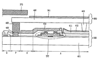
以下、図1を参照して本発明に係るCOT構造液晶表示装置の構造に対し、説明する。 The structure of the COT structure liquid crystal display device according to the present invention will be described below with reference to FIG.
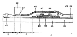
本発明に係る液晶表示装置は、カラーフィルター層を包含するアレイ基板とこれに対向するカラーフィルター基板とがシールパターン460により貼り合わせられている。また、アレイ基板には、複数のゲートライン(図示せず)とゲートラインと垂直交差するデータライン(図示せず)が形成される。ゲートラインとデータラインとの交差により単位画素が定義されて、単位画素の一方側にスイッチング素子である薄膜トランジスタ(TFT)が形成されている。
In the liquid crystal display device according to the present invention, an array substrate including a color filter layer and a color filter substrate facing the array substrate are bonded together by a
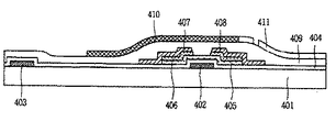
図1は、TFTを包含する一つの単位画素と画素領域外郭部を示している。単位画素にデータ電圧を印加するソース及びドレイン電極を包含するTFTは、保護層409により外部と絶縁されている。また、保護層409の上部には、ゲートライン及びデータラインなどの反転ドメイン領域を遮るブラックマトリックス410が形成されるが、ブラックマトリックス410は、TFTが形成される領域を一層遮っている。また、ブラックマトリックス410は、マトリックス状に配列されて、反転ドメイン領域を遮る。また、単位画素領域には、赤、緑、青色のカラーフィルター層411のうち何れか一つが形成される。
FIG. 1 shows one unit pixel including a TFT and a pixel region outline. The TFT including the source and drain electrodes for applying the data voltage to the unit pixel is insulated from the outside by the
また、単位画素毎に形成されるカラーフィルター層411上には、画素電極412が形成されて、画素電極412は、TFTのドレイン電極と連結される。
A
一方、本発明のブラックマトリックス410は、画素領域だけではなく、画素領域外郭部0に延長されて形成される。また、ブラックマトリックス410が画素領域外郭部0に延長されて形成されることで、画素領域外郭部0を通って光漏れが発生することを防止することができる。
On the other hand, the
ところで、従来は、画素領域外郭部0に静電気放電回路(ESD)が形成されていて、ブラックマトリックスを画素領域外郭部に設置することが困難であった。静電気放電回路は、複数の薄膜トランジスタの組合により形成されるが、その一電極がゲートパッド部又はデータパッド部と連結され、他の電極は画素領域のゲートライン及びデータライン又は上部基板の共通電極などと連結されて、外部から流入される静電気を放電させる役割をする。また、静電気放電回路は、画素電極物質のITO(Indium Tin Oxide)によりパッド部及び画素領域内の複数の配線と連結される。連結は、保護層409上に形成される複数のコンタクトホール(図示せず)を通って行われる。
Conventionally, an electrostatic discharge circuit (ESD) is formed in the pixel region
ところが、保護層409上に厚い有機膜であるブラックマトリックス410が形成されると、コンタクトホールを形成することが難しい。即ち、画素領域内の各種配線及び上部基板に形成される各種配線と静電気防止回路とを連結するためのコンタクトホールは、ブラックマトリックス410及びその下方の保護層409を除去して形成するべきである。
However, when the
しかし、ブラックマトリックス410は、厚いだけではなく、微細な蝕刻が難しくて静電気防止回路を露出させるコンタクトホールを形成することができない。
However, the
従って、本発明は、静電気放電回路を画素領域外郭部0に形成しない。即ち、図1に示すように、本発明に係る静電気防止回路450は、画素領域外郭部0に延長されるブラックマトリックス410の外郭に形成される。特に、画素領域外郭部0とパッド部Q間に上部基板と下部基板とを貼り合わせるシールパターン460が形成されるが、本発明の静電気放電回路450は、シールパターン460下に形成されることができる。
Therefore, the present invention does not form an electrostatic discharge circuit in the pixel region
また、シールパターン460は、静電気防止回路部と画素領域の各種配線及び上部基板の各種配線がITO配線により相互連結された後に形成されるために、静電気防止回路部450上にシールパターン460を形成することは可能である。
Further, since the
従って、本発明は、シールパターン形成工程の順序を変化させてブラックマトリックス410を画素領域外郭部0に延長して形成しながらも、ブラックマトリックス410により覆われない静電気放電回路450を構成することができる。
Accordingly, the present invention can constitute the
また、シールパターン460の外郭においては、ゲート信号及びデータ信号が入力されるゲートパッド部又はデータパッド部などが形成されるパッド部Qが更に形成されている。
In addition, a pad portion Q in which a gate pad portion or a data pad portion to which a gate signal and a data signal are input is formed is formed on the outer surface of the
一方、TFTアレイ基板500の上部には、共通電極を包含する上部基板600が位置するが、上部基板は、透明なガラスなどの基板480とアレイ基板500に形成される画素電極412と共に液晶に電界を印加する共通電極(図示せず)及び液晶の初期配向のための配向膜(図示せず)を包含して構成される。
On the other hand, an
また、上部基板600とアレイ基板500は、シールパターン460により互いに貼り合わせられ、その間に液晶が注入される。上部基板600とアレイ基板500のセルギャップを誘起するために上部基板600又はアレイ基板500には、複数のスペーサ483が更に形成される。
The
また、上部基板500の外面には偏光板361が形成されるが、偏光板361は、アレイ基板500の外部にも更に形成される。
Further, a
また、上部基板600とアレイ基板500との貼り合わせにより形成される液晶表示パネルは、モジュール装置により保護されるが、モジュール装置の中の一つが液晶表示パネルの上部から液晶表示パネルの縁を遮るトップケース370である。また、トップケース370は、液晶パネルを外部の衝撃から保護する機能をすると共に、アレイ基板500の画素領域外郭部0から発生する光漏れを防止することができる。
The liquid crystal display panel formed by bonding the
しかし、上部基板に形成される偏光板361との接触を避けるために、トップケース370は、画素領域外郭部0を完全に遮ることができない。従って、本発明の画素領域外郭部0に形成されるブラックマトリックス410は必要である。
However, in order to avoid contact with the
一方、本発明は、トップケース370の形成位置を調節して静電気放電回路の形成位置を調節することができる。
Meanwhile, the present invention can adjust the formation position of the electrostatic discharge circuit by adjusting the formation position of the
本発明の他の実施形態は、静電気放電回路450をシールパターン460の前段に形成することを提案する。
Another embodiment of the present invention proposes to form the
以下、図2を参照して本発明の他の実施形態に係る液晶表示装置の構成に対し、説明する。 Hereinafter, a configuration of a liquid crystal display device according to another embodiment of the present invention will be described with reference to FIG.
本発明に係る液晶表示装置の基本構成は、実施形態と同様であるため、重複する構成要素の説明は省略する。 Since the basic configuration of the liquid crystal display device according to the present invention is the same as that of the embodiment, description of overlapping components is omitted.
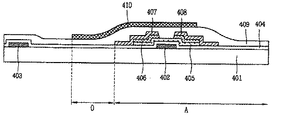
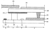
アレイ基板500上には、図2に示すように、画素領域Aとシールパターン460が形成されるシールライン形成領域Pと、シールライン形成領域Pと画素領域A間に形成される画素領域外郭部0と、ゲート電圧又はデータ電圧が印加されるパッド部Qと、が形成される。画素領域外郭部0の中で、シールパターン460に隣接して静電気放電回路450が形成される。静電気放電回路450を除外した画素領域外郭部0の残りの領域は、ブラックマトリックス410により遮られる。
On the
一方、液晶パネルの外郭を覆うトップケースは、延長されて静電気放電回路450が形成される画素領域外郭部0の一部を遮る。また、トップケースは、上部基板の偏光板361と接触しない範囲でより延長されることができる。
On the other hand, the top case covering the outer periphery of the liquid crystal panel is extended to block a part of the pixel region
従って、トップケース370とブラックマトリックス410により画素領域外郭部0の光漏れを防止することができる。
Therefore, the
製品によってはシールライン形成領域Pからパッド部Qに至るリンク部(図示せず)が更に形成され得る。リンク部は、ゲートライン間又はデータライン間の間隔が狭くなりながらパッド部と連結される所である。従って、リンク部は、空間が狭くて静電気放電回路を形成することが難しいが、本発明は、リンク部ではない画素領域外郭部0に静電気放電回路が形成されるため、静電気放電回路を形成するための空間を十分に確保することができる。しかし、静電気放電回路がシールライン形成部P又は画素領域外郭部0に形成されることで制限されることない。即ち、デザインルールを改善して静電気防止回路を微細線幅に設計する場合、リンク部に形成されることもできる。
Depending on the product, a link portion (not shown) from the seal line forming region P to the pad portion Q may be further formed. The link part is a place connected to the pad part while the interval between the gate lines or the data lines is narrowed. Accordingly, although the link portion has a narrow space and it is difficult to form an electrostatic discharge circuit, the present invention forms an electrostatic discharge circuit because the electrostatic discharge circuit is formed in the pixel region
以下、本発明に係るCOT構造液晶表示装置の製造工程に対し、図3A〜図3Gを参照して説明する。 Hereinafter, the manufacturing process of the COT structure liquid crystal display device according to the present invention will be described with reference to FIGS. 3A to 3G.
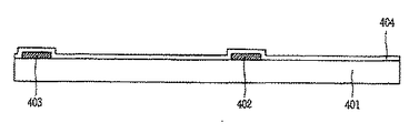
図3Aに示すように、ガラスなどの透明な基板401上にゲート電極402及びゲートパッド電極403を形成する。ゲート電極402は、金属箔膜をスパッタリング方法により蒸着してフォトリソグラフィ工程を利用して所定のパターンに形成することができる。
As shown in FIG. 3A, a
次いで、ゲート電極402上にシリコン酸化膜のゲート絶縁層404をプラズマ化学気相蒸着方法(PECVD)方法により形成する。
Next, a
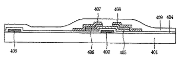
次いで、図3Bに示すように、ゲート電極402上にアクティブ層405とオームコンタクト層406を形成する。アクティブ層405は、半導体層から構成されて、 PECVD 方法により蒸着されてドライエッチングプロセスによってパターニングされることができる。
Next, as shown in FIG. 3B, an
次に、図3Cに示すように、スパッタリング方法により金属箔膜を蒸着し、フォトリソグラフィ工程によりソース及びドレイン電極407、408を形成し、画素領域にはデータライン(図示せず)を形成する。
Next, as shown in FIG. 3C, a metal foil film is deposited by a sputtering method, source and drain
次いで、ソース及びドレイン電極407、408上に絶縁層の保護層409を更に形成する。
Next, an insulating
一方、図3A〜図3Cには、図示されなかっが、TFTが形成される画素領域外郭部に静電気放電回路が共に形成されることもできる。静電気放電回路も保護層409により保護される。
On the other hand, although not shown in FIGS. 3A to 3C, an electrostatic discharge circuit may be formed at the outer portion of the pixel region where the TFT is formed. The electrostatic discharge circuit is also protected by the
次いで、図3Dに示すように、保護層409上、特に、画素領域Aに有機膜から構成されるブラックマトリックス410を形成する。ブラックマトリックスは、格子状に構成されて、ゲートライン及びデータラインを遮って反転ドメイン領域であるゲートライン及びデータラインの隣接部を遮る。且つ、ブラックマトリックス410は、延長されて画素領域外郭部0も同時に遮る。
Next, as shown in FIG. 3D, a
ブラックマトリックス410を形成した後、ブラックマトリックスの間、即ち、単位画素毎にカラーフィルター層411を形成する。カラーフィルター層411は、赤、緑、青色のサブカラーフィルター層をフォトマスク工程を適用して分散法により形成することができる。
After the
カラーフィルター層を形成する工程において、TFTの所定領域にはカラーフィルター層が形成されないようにする。 In the step of forming the color filter layer, the color filter layer is not formed in a predetermined region of the TFT.
次いで、TFTのドレイン電極408を露出させるコンタクトホールを形成する。コンタクトホールは、カラーフィルター層が形成されない領域に形成して保護層のみの除去により容易に形成することができる。
Next, a contact hole that exposes the
コンタクトホールが形成される段階において、静電気放電回路部の一電極を露出させるコンタクトホールが同時に形成される。また、ゲートパッド電極を露出させるコンタクトホールも共に形成される。 At the stage where the contact hole is formed, a contact hole that exposes one electrode of the electrostatic discharge circuit portion is simultaneously formed. A contact hole for exposing the gate pad electrode is also formed.
次いで、図3Fに示すように、コンタクトホールを通ってドレイン電極と連結されて単位画素毎に形成される画素電極412を形成する。画素電極は、透明電極であるITOをスパッタリングして蒸着した後、フォトリソグラフィ工程を適用してパターニングする。画素電極がパターニングされる段階において、パッド部のパッド及び静電気放電回路と画素領域の配線とを連結する静電気放電回路の連結配線が同時に形成される。
Next, as shown in FIG. 3F, a
次いで、ポリイミド(polyimide)から構成される配向膜を画素電極が形成されたアレイ基板上に形成することで、TFTアレイ基板を完成する。 Next, an alignment film made of polyimide is formed on the array substrate on which the pixel electrodes are formed, thereby completing the TFT array substrate.
一方、TFTアレイ基板と対向する上部基板が別途の工程によって形成される。上部基板には、共通電極481が形成され、且つ、配向膜482が更に形成される。本発明の上部基板には、画素領域外郭部の光漏れの防止のためのブラックマトリックスが形成されないことが特徴である。
On the other hand, an upper substrate facing the TFT array substrate is formed by a separate process. A
次いで、別途の工程により形成された上部基板とアレイ基板をシールパターンを通って貼り合わせる工程を進行する。貼り合わせ工程は、シールラインの形成工程、上部基板とアレイ基板のアライン工程及び貼り合わせ工程によって形成される。 Next, a process of bonding the upper substrate formed in a separate process and the array substrate through a seal pattern is performed. The bonding process is formed by a seal line forming process, an alignment process between the upper substrate and the array substrate, and a bonding process.
貼り合わせ工程の後、液晶パネルのセルギャップに液晶を充填させて切断して単位液晶パネルを完成する。 After the bonding step, liquid crystal is filled in the cell gap of the liquid crystal panel and cut to complete the unit liquid crystal panel.
409:保護層
410:ブラックマトリックス
411:カラーフィルター層
412:画素電極
450:静電気防止回路部
460:シールパターン
481:共通電極
409: Protective layer 410: Black matrix 411: Color filter layer 412: Pixel electrode 450: Antistatic circuit 460: Seal pattern 481: Common electrode
Claims (8)
前記アレイ基板上に形成されたゲートライン及び該ゲートラインと垂直交差するデータラインと、
前記アレイ基板上に形成され、前記ゲートライン及び前記ゲートラインと垂直交差するデータラインにより画定される単位画素がマトリックス配列される画素領域と、
前記アレイ基板上に形成され、前記ゲートライン及びデータラインとそれぞれ連結されて、前記画素領域の外郭に形成されるパッド部と、
前記アレイ基板上に形成され、前記アレイ基板上の画素領域にゲート電極、アクティブ層、及び該アクティブ層と連結されたソース及びドレイン電極を備える薄膜トランジスタと、
前記アレイ基板の全面に形成された保護層と、
前記保護層上に形成され、前記画素領域と前記パッド部間に定義されるシールパターン形成領域に配置される静電気防止回路部と、
前記保護層上に形成され、前記画素領域から前記画素領域外郭部まで延びたブラックマトリクスと、
前記静電気防止回路部を含む保護層上に形成され、前記パッド部と前記画素領域間に定義される前記シールパターン形成領域に形成されるシールパターンと、
前記保護層上に形成され、前記ブラックマトリクス間に形成されるカラーフィルタ層とを包含して構成されることを特徴とするCOT構造液晶表示素子。
An array substrate and an upper substrate bonded to the array substrate;
A gate line formed on the array substrate and a data line perpendicularly intersecting the gate line;
A pixel region formed on the array substrate, in which unit pixels defined by the gate lines and data lines perpendicularly intersecting the gate lines are arranged in a matrix;
A pad portion formed on the array substrate, connected to the gate line and the data line, and formed on the outer periphery of the pixel region;
A thin film transistor formed on the array substrate and including a gate electrode, an active layer, and a source and drain electrode connected to the active layer in a pixel region on the array substrate;
A protective layer formed on the entire surface of the array substrate;
An antistatic circuit portion formed on the protective layer and disposed in a seal pattern forming region defined between the pixel region and the pad portion;
A black matrix formed on the protective layer and extending from the pixel region to the outer region of the pixel region;
A seal pattern formed on a protective layer including the antistatic circuit portion and formed in the seal pattern formation region defined between the pad portion and the pixel region;
A COT structure liquid crystal display element comprising a color filter layer formed on the protective layer and formed between the black matrices.
2. The COT structure liquid crystal display device according to claim 1, wherein the antistatic circuit portion is formed under the seal pattern.
2. The COT structure liquid crystal display device according to claim 1, further comprising a top case that blocks an outer portion of the pixel region.
2. The COT structure liquid crystal display device according to claim 1, further comprising a top case that blocks an outer portion of the pixel region.
2. The COT-structured liquid crystal display device according to claim 1, wherein the static electricity prevention circuit unit is not blocked by the black matrix.
前記アレイ基板上に単位画素がマトリクス配列される画素領域を定義するゲートライン及び該ゲートラインと垂直交差するデータラインを形成する段階と、
前記アレイ基板上に、前記アレイ基板上の画素領域にゲート電極、アクティブ層、及び該アクティブ層と連結されたソース及びドレイン電極を備える薄膜トランジスタを形成する段階と、
前記アレイ基板上に、前記ゲートライン及び前記データラインとそれぞれ連結され、前記画素領域の外郭にパッド部を形成する段階と、
前記アレイ基板の全面に保護層を形成する段階と、
前記保護層上に、前記画素領域と前記パッド部間に定義されるシールパターン形成領域に静電気防止回路部を形成する段階と、
前記保護層上に、前記画素領域から前記画素領域外郭部まで延びるブラックマトリクスを形成する段階と、
前記保護層上に、前記ブラックマトリクス間にカラーフィルタ層を形成する段階と、
前記カラーフィルタ層上に前記薄膜トランジスタのドレイン電極と連結される画素電極を形成する段階と、
前記パッド部と前記画素領域間に定義される前記シールパターン形成領域である前記静電気防止回路部を含む保護層上に、シールパターンを形成する段階と、
前記シールパターンにより前記アレイ基板と前記上部基板を貼り合わせる段階と
から構成されることを特徴とするCOT構造液晶表示装置製造方法。
Providing an array substrate and an upper substrate bonded to the array substrate;
Forming a gate line defining a pixel region in which unit pixels are arranged in a matrix on the array substrate and a data line perpendicularly intersecting the gate line;
Forming a thin film transistor including a gate electrode, an active layer, and a source and drain electrode connected to the active layer in a pixel region on the array substrate;
On the array substrate, the gate line and the data line are connected to each other, and a pad portion is formed on the outer periphery of the pixel region;
Forming a protective layer on the entire surface of the array substrate;
On the protective layer, forming an antistatic circuit portion in a seal pattern forming region defined between the pixel region and the pad portion;
Forming a black matrix on the protective layer extending from the pixel region to the outer region of the pixel region;
Forming a color filter layer between the black matrix on the protective layer;
Forming a pixel electrode connected to the drain electrode of the thin film transistor on the color filter layer;
Forming a seal pattern on a protective layer including the antistatic circuit portion which is the seal pattern forming region defined between the pad portion and the pixel region;
A method of manufacturing a COT-structured liquid crystal display device, comprising: bonding the array substrate and the upper substrate with the seal pattern.
前記アレイ基板上に共通電極を形成する段階と、
前記共通電極上に配向膜を形成する段階と、を順次行うことを特徴とする請求項6記載のCOT構造液晶表示装置製造方法。
The step of forming the upper substrate includes:
Forming a common electrode on the array substrate;
7. The method of manufacturing a COT structure liquid crystal display device according to claim 6, wherein the step of forming an alignment film on the common electrode is sequentially performed.
Applications Claiming Priority (1)
| Application Number | Priority Date | Filing Date | Title |
|---|---|---|---|
| KR1020040049779A KR100945354B1 (en) | 2004-06-29 | 2004-06-29 | Color filter on tft type liquid crystal display device comprising black matrix formed on outside portion of active area and method for fabricating therefor |
Related Parent Applications (1)
| Application Number | Title | Priority Date | Filing Date |
|---|---|---|---|
| JP2005185929A Division JP4477552B2 (en) | 2004-06-29 | 2005-06-27 | COT-structured liquid crystal display device for preventing light leakage from outer portion of pixel region and manufacturing method thereof |
Publications (2)
| Publication Number | Publication Date |
|---|---|
| JP2010055100A true JP2010055100A (en) | 2010-03-11 |
| JP4643738B2 JP4643738B2 (en) | 2011-03-02 |
Family
ID=35505270
Family Applications (2)
| Application Number | Title | Priority Date | Filing Date |
|---|---|---|---|
| JP2005185929A Active JP4477552B2 (en) | 2004-06-29 | 2005-06-27 | COT-structured liquid crystal display device for preventing light leakage from outer portion of pixel region and manufacturing method thereof |
| JP2009254704A Active JP4643738B2 (en) | 2004-06-29 | 2009-11-06 | COT-structured liquid crystal display device for preventing light leakage from outer portion of pixel region and manufacturing method thereof |
Family Applications Before (1)
| Application Number | Title | Priority Date | Filing Date |
|---|---|---|---|
| JP2005185929A Active JP4477552B2 (en) | 2004-06-29 | 2005-06-27 | COT-structured liquid crystal display device for preventing light leakage from outer portion of pixel region and manufacturing method thereof |
Country Status (4)
| Country | Link |
|---|---|
| US (2) | US8102489B2 (en) |
| JP (2) | JP4477552B2 (en) |
| KR (1) | KR100945354B1 (en) |
| CN (1) | CN100381894C (en) |
Cited By (2)
| Publication number | Priority date | Publication date | Assignee | Title |
|---|---|---|---|---|
| US20130113917A1 (en) * | 2010-06-29 | 2013-05-09 | Japan Tobacco Inc. | Cigarette inspection apparatus |
| JP2015036819A (en) * | 2013-08-14 | 2015-02-23 | 三星ディスプレイ株式會社Samsung Display Co.,Ltd. | Thin film transistor display panel |
Families Citing this family (29)
| Publication number | Priority date | Publication date | Assignee | Title |
|---|---|---|---|---|
| KR100945354B1 (en) * | 2004-06-29 | 2010-03-08 | 엘지디스플레이 주식회사 | Color filter on tft type liquid crystal display device comprising black matrix formed on outside portion of active area and method for fabricating therefor |
| TWI261920B (en) * | 2005-07-07 | 2006-09-11 | Au Optronics Corp | Active device matrix substrate |
| KR101300819B1 (en) * | 2006-12-05 | 2013-08-26 | 삼성디스플레이 주식회사 | Liquid crystal display and method of manufacturing the same |
| KR101430526B1 (en) * | 2006-12-28 | 2014-08-19 | 삼성디스플레이 주식회사 | Display substrate and display apparatus having the same |
| KR101386576B1 (en) * | 2008-06-25 | 2014-04-18 | 엘지디스플레이 주식회사 | Liquid crystal display panel |
| JP5195260B2 (en) * | 2008-10-14 | 2013-05-08 | セイコーエプソン株式会社 | Electronics |
| KR101607636B1 (en) | 2009-11-23 | 2016-04-12 | 삼성디스플레이 주식회사 | Liquid crystal display |
| KR101662135B1 (en) * | 2010-01-15 | 2016-10-05 | 삼성디스플레이 주식회사 | Electrophoretic display panel, method of manufacturing the same and electrophoretic display apparatus having the same |
| KR101620526B1 (en) | 2010-01-22 | 2016-05-13 | 삼성디스플레이 주식회사 | Method of making liquid crystal display and liquid crystal display thereof |
| CN102722056A (en) * | 2011-03-29 | 2012-10-10 | 京东方科技集团股份有限公司 | A color light-filtering array base plate, a manufacture method thereof, and a liquid-crystal display panel |
| JP6028332B2 (en) | 2012-01-12 | 2016-11-16 | セイコーエプソン株式会社 | Liquid crystal device and electronic device |
| KR101982095B1 (en) * | 2012-10-17 | 2019-05-24 | 엘지디스플레이 주식회사 | Liquid crystal display having seal pattern |
| KR101973009B1 (en) | 2012-11-13 | 2019-04-29 | 삼성디스플레이 주식회사 | Liquid crystal display device |
| JP2014106428A (en) * | 2012-11-28 | 2014-06-09 | Japan Display Inc | Display device and electronic device |
| KR102029437B1 (en) * | 2012-12-17 | 2019-10-07 | 엘지디스플레이 주식회사 | Touch sensor integrated type display device |
| TWI473057B (en) * | 2013-01-30 | 2015-02-11 | Au Optronics Corp | Pixel unit and pixel array |
| KR102040084B1 (en) | 2013-03-25 | 2019-11-05 | 삼성디스플레이 주식회사 | Display device |
| KR102089326B1 (en) * | 2013-10-01 | 2020-03-17 | 엘지디스플레이 주식회사 | Display Device |
| KR102124405B1 (en) * | 2013-11-11 | 2020-06-19 | 삼성디스플레이 주식회사 | Liquid crystal display apparatus |
| KR102127240B1 (en) * | 2013-12-13 | 2020-06-26 | 엘지디스플레이 주식회사 | Display device, signal line and method of fabricating thereof |
| KR102308669B1 (en) * | 2014-12-05 | 2021-10-05 | 엘지디스플레이 주식회사 | Organic light emitting display device and method of fabricating the same |
| KR102441558B1 (en) | 2015-04-07 | 2022-09-08 | 삼성디스플레이 주식회사 | Organic light-emitting display apparatus and method for manufacturing the same |
| CN104950541B (en) * | 2015-07-20 | 2018-05-01 | 深圳市华星光电技术有限公司 | BOA type liquid crystal display panels and preparation method thereof |
| KR102630945B1 (en) * | 2015-11-20 | 2024-01-30 | 주식회사 동진쎄미켐 | Photosensitive resin composition |
| CN105445998A (en) * | 2015-12-31 | 2016-03-30 | 武汉华星光电技术有限公司 | LTPS display panel and making process thereof |
| CN106200160A (en) * | 2016-07-08 | 2016-12-07 | 京东方科技集团股份有限公司 | Array base palte, display floater and display device |
| KR102554095B1 (en) | 2016-09-30 | 2023-07-10 | 엘지디스플레이 주식회사 | In-cell touch liquid crystal display device and method for fabricating the same |
| CN106353944A (en) * | 2016-11-04 | 2017-01-25 | 京东方科技集团股份有限公司 | Array base plate, manufacturing method of array base plate, display panel and display device |
| KR20210134175A (en) | 2020-04-29 | 2021-11-09 | 삼성디스플레이 주식회사 | Display apparatus |
Citations (1)
| Publication number | Priority date | Publication date | Assignee | Title |
|---|---|---|---|---|
| JP2006018275A (en) * | 2004-06-29 | 2006-01-19 | Lg Phillips Lcd Co Ltd | Cot type liquid crystal display device which prevents light from leaking outside pixel region and method for fabricating same |
Family Cites Families (24)
| Publication number | Priority date | Publication date | Assignee | Title |
|---|---|---|---|---|
| JPH05241139A (en) * | 1992-02-27 | 1993-09-21 | Canon Inc | Liquid crystal display device |
| JPH07311378A (en) * | 1994-05-18 | 1995-11-28 | Toppan Printing Co Ltd | Liquid crystal display device |
| WO1997006465A1 (en) * | 1995-08-07 | 1997-02-20 | Hitachi, Ltd. | Active matrix type liquid crystal display device resistant to static electricity |
| JP3663741B2 (en) * | 1996-05-22 | 2005-06-22 | セイコーエプソン株式会社 | Active matrix type liquid crystal display device and manufacturing method thereof |
| JPH1010516A (en) * | 1996-06-20 | 1998-01-16 | Nec Corp | Color liquid crystal display device |
| KR100218697B1 (en) * | 1996-09-23 | 1999-09-01 | 구자홍 | Liquid crystal display elements |
| US5907379A (en) * | 1996-10-21 | 1999-05-25 | Samsung Electronics Co., Ltd. | In-plane switching liquid crystal display having high aperture ratio |
| JP3343645B2 (en) * | 1997-03-25 | 2002-11-11 | シャープ株式会社 | Liquid crystal display device and method of manufacturing the same |
| TW440736B (en) * | 1997-10-14 | 2001-06-16 | Samsung Electronics Co Ltd | Liquid crystal displays and manufacturing methods thereof |
| KR100280891B1 (en) * | 1998-02-25 | 2001-02-01 | 구본준 | LCD Display Case |
| JP3471692B2 (en) * | 2000-01-21 | 2003-12-02 | Nec液晶テクノロジー株式会社 | Color liquid crystal display panel |
| DE10124986B4 (en) * | 2000-05-25 | 2005-03-10 | Lg Philips Lcd Co | Liquid crystal display device and manufacturing method therefor |
| JP2002026333A (en) * | 2000-07-11 | 2002-01-25 | Nec Corp | Method of manufacturing active matrix board |
| KR100628259B1 (en) * | 2000-11-22 | 2006-09-27 | 엘지.필립스 엘시디 주식회사 | Liquid Crystal Display Panel |
| JP2002296618A (en) * | 2001-03-29 | 2002-10-09 | Nec Corp | Liquid crystal display device and its manufacturing method |
| JPWO2003030131A1 (en) * | 2001-08-29 | 2005-01-20 | セイコーエプソン株式会社 | Electro-optical device and electronic apparatus |
| KR100430804B1 (en) * | 2001-11-15 | 2004-05-10 | 엘지.필립스 엘시디 주식회사 | Liquid Crystal Display Device having improved Aperture Ratio |
| JP3808356B2 (en) * | 2001-12-04 | 2006-08-09 | 株式会社日立製作所 | Liquid crystal display |
| KR100830524B1 (en) * | 2001-12-29 | 2008-05-21 | 엘지디스플레이 주식회사 | Preventive Structure of Liquid Crystal Display Device for Light Leakage |
| KR20040009858A (en) * | 2002-07-26 | 2004-01-31 | 비오이 하이디스 테크놀로지 주식회사 | Liquid crystal display |
| TW200410029A (en) * | 2002-12-05 | 2004-06-16 | Chunghwa Picture Tubes Ltd | Liquid crystal displayer with ink jet color filter and manufacture method thereof |
| GB2396244B (en) * | 2002-12-09 | 2006-03-22 | Lg Philips Lcd Co Ltd | Array substrate having color filter on thin film transistor s tructure for LCD device and method of fabricating the same |
| US6933993B2 (en) * | 2003-05-16 | 2005-08-23 | Toppoly Optoelectronics Corp. | Method of forming a color filter layer on an array substrate and device thereof |
| KR100717184B1 (en) * | 2003-08-01 | 2007-05-11 | 비오이 하이디스 테크놀로지 주식회사 | Liquid crystal display panel |
-
2004
- 2004-06-29 KR KR1020040049779A patent/KR100945354B1/en active IP Right Grant
-
2005
- 2005-06-22 US US11/158,009 patent/US8102489B2/en active Active
- 2005-06-27 JP JP2005185929A patent/JP4477552B2/en active Active
- 2005-06-28 CN CNB2005100802709A patent/CN100381894C/en not_active Expired - Fee Related
-
2009
- 2009-11-06 JP JP2009254704A patent/JP4643738B2/en active Active
-
2012
- 2012-01-03 US US13/342,596 patent/US8284376B2/en active Active
Patent Citations (2)
| Publication number | Priority date | Publication date | Assignee | Title |
|---|---|---|---|---|
| JP2006018275A (en) * | 2004-06-29 | 2006-01-19 | Lg Phillips Lcd Co Ltd | Cot type liquid crystal display device which prevents light from leaking outside pixel region and method for fabricating same |
| JP4477552B2 (en) * | 2004-06-29 | 2010-06-09 | エルジー ディスプレイ カンパニー リミテッド | COT-structured liquid crystal display device for preventing light leakage from outer portion of pixel region and manufacturing method thereof |
Cited By (3)
| Publication number | Priority date | Publication date | Assignee | Title |
|---|---|---|---|---|
| US20130113917A1 (en) * | 2010-06-29 | 2013-05-09 | Japan Tobacco Inc. | Cigarette inspection apparatus |
| US9699416B2 (en) * | 2010-06-29 | 2017-07-04 | Japan Tobacco Inc. | Cigarette inspection apparatus |
| JP2015036819A (en) * | 2013-08-14 | 2015-02-23 | 三星ディスプレイ株式會社Samsung Display Co.,Ltd. | Thin film transistor display panel |
Also Published As
| Publication number | Publication date |
|---|---|
| US20120105394A1 (en) | 2012-05-03 |
| JP4643738B2 (en) | 2011-03-02 |
| US8102489B2 (en) | 2012-01-24 |
| KR100945354B1 (en) | 2010-03-08 |
| JP4477552B2 (en) | 2010-06-09 |
| US20050285995A1 (en) | 2005-12-29 |
| KR20060000808A (en) | 2006-01-06 |
| CN1716015A (en) | 2006-01-04 |
| US8284376B2 (en) | 2012-10-09 |
| JP2006018275A (en) | 2006-01-19 |
| CN100381894C (en) | 2008-04-16 |
Similar Documents
| Publication | Publication Date | Title |
|---|---|---|
| JP4643738B2 (en) | COT-structured liquid crystal display device for preventing light leakage from outer portion of pixel region and manufacturing method thereof | |
| JP4059676B2 (en) | Liquid crystal display | |
| JP5392670B2 (en) | Liquid crystal display device and manufacturing method thereof | |
| JP4925030B2 (en) | Liquid crystal display device and manufacturing method thereof | |
| KR100884541B1 (en) | Liquid Crystal Display Device and Method for fabricating the same | |
| JP2006201312A (en) | Liquid crystal display panel and liquid crystal display device | |
| JP2004272012A (en) | Display apparatus | |
| JP2004205552A (en) | Picture display panel, picture display device and method for manufacturing picture display panel | |
| KR101423909B1 (en) | Display substrate and liquid crystal display device having the same | |
| KR20080019838A (en) | Short pad and thin film transistor substrate and liquid crystal display having the same | |
| JP2009151285A (en) | Liquid crystal display device and method for manufacturing the same | |
| US9897866B2 (en) | Liquid crystal display and method for manufacturing the same | |
| KR100951840B1 (en) | Liquid Crystal Display Device | |
| JP5275650B2 (en) | Liquid crystal display | |
| JP2010096944A (en) | Liquid crystal panel | |
| JP5207947B2 (en) | Liquid crystal display device and manufacturing method thereof | |
| JP2009169162A (en) | Liquid crystal display | |
| KR20080048725A (en) | In-plane switching mode liquid crystal display device | |
| KR20060019819A (en) | Liquid crystal display device | |
| JPH07199222A (en) | Liquid crystal display device | |
| KR100303447B1 (en) | LCD with static electricity protection circuit | |
| KR100482343B1 (en) | Thin film transistor array substrate for protecting loading effect and manufacturing method thereof | |
| KR100558716B1 (en) | Liquid crystal display panel and fabricating method thereof | |
| KR20040051073A (en) | Array substrate for LCD and Method for fabricating of the same | |
| JP2002182242A (en) | Method for producing liquid crystal display |
Legal Events
| Date | Code | Title | Description |
|---|---|---|---|
| A621 | Written request for application examination |
Free format text: JAPANESE INTERMEDIATE CODE: A621 Effective date: 20091204 |
|
| A521 | Request for written amendment filed |
Free format text: JAPANESE INTERMEDIATE CODE: A523 Effective date: 20091222 |
|
| A131 | Notification of reasons for refusal |
Free format text: JAPANESE INTERMEDIATE CODE: A132 Effective date: 20100712 |
|
| A521 | Request for written amendment filed |
Free format text: JAPANESE INTERMEDIATE CODE: A523 Effective date: 20101012 |
|
| TRDD | Decision of grant or rejection written | ||
| A01 | Written decision to grant a patent or to grant a registration (utility model) |
Free format text: JAPANESE INTERMEDIATE CODE: A01 Effective date: 20101108 |
|
| A01 | Written decision to grant a patent or to grant a registration (utility model) |
Free format text: JAPANESE INTERMEDIATE CODE: A01 |
|
| A61 | First payment of annual fees (during grant procedure) |
Free format text: JAPANESE INTERMEDIATE CODE: A61 Effective date: 20101202 |
|
| R150 | Certificate of patent or registration of utility model |
Ref document number: 4643738 Country of ref document: JP Free format text: JAPANESE INTERMEDIATE CODE: R150 Free format text: JAPANESE INTERMEDIATE CODE: R150 |
|
| FPAY | Renewal fee payment (event date is renewal date of database) |
Free format text: PAYMENT UNTIL: 20131210 Year of fee payment: 3 |
|
| R250 | Receipt of annual fees |
Free format text: JAPANESE INTERMEDIATE CODE: R250 |
|
| R250 | Receipt of annual fees |
Free format text: JAPANESE INTERMEDIATE CODE: R250 |
|
| R250 | Receipt of annual fees |
Free format text: JAPANESE INTERMEDIATE CODE: R250 |
|
| R250 | Receipt of annual fees |
Free format text: JAPANESE INTERMEDIATE CODE: R250 |
|
| R250 | Receipt of annual fees |
Free format text: JAPANESE INTERMEDIATE CODE: R250 |
|
| R250 | Receipt of annual fees |
Free format text: JAPANESE INTERMEDIATE CODE: R250 |
|
| R250 | Receipt of annual fees |
Free format text: JAPANESE INTERMEDIATE CODE: R250 |
|
| R250 | Receipt of annual fees |
Free format text: JAPANESE INTERMEDIATE CODE: R250 |
|
| R250 | Receipt of annual fees |
Free format text: JAPANESE INTERMEDIATE CODE: R250 |
|
| R250 | Receipt of annual fees |
Free format text: JAPANESE INTERMEDIATE CODE: R250 |
|
| R250 | Receipt of annual fees |
Free format text: JAPANESE INTERMEDIATE CODE: R250 |