JP2010050362A - Multibeam semiconductor laser - Google Patents
Multibeam semiconductor laser Download PDFInfo
- Publication number
- JP2010050362A JP2010050362A JP2008214701A JP2008214701A JP2010050362A JP 2010050362 A JP2010050362 A JP 2010050362A JP 2008214701 A JP2008214701 A JP 2008214701A JP 2008214701 A JP2008214701 A JP 2008214701A JP 2010050362 A JP2010050362 A JP 2010050362A
- Authority
- JP
- Japan
- Prior art keywords
- semiconductor laser
- layer
- electrodes
- electrode
- insulating film
- Prior art date
- Legal status (The legal status is an assumption and is not a legal conclusion. Google has not performed a legal analysis and makes no representation as to the accuracy of the status listed.)
- Granted
Links
Images


Classifications
-
- H—ELECTRICITY
- H01—ELECTRIC ELEMENTS
- H01S—DEVICES USING THE PROCESS OF LIGHT AMPLIFICATION BY STIMULATED EMISSION OF RADIATION [LASER] TO AMPLIFY OR GENERATE LIGHT; DEVICES USING STIMULATED EMISSION OF ELECTROMAGNETIC RADIATION IN WAVE RANGES OTHER THAN OPTICAL
- H01S5/00—Semiconductor lasers
- H01S5/02—Structural details or components not essential to laser action
- H01S5/024—Arrangements for thermal management
- H01S5/02476—Heat spreaders, i.e. improving heat flow between laser chip and heat dissipating elements
-
- H—ELECTRICITY
- H01—ELECTRIC ELEMENTS
- H01S—DEVICES USING THE PROCESS OF LIGHT AMPLIFICATION BY STIMULATED EMISSION OF RADIATION [LASER] TO AMPLIFY OR GENERATE LIGHT; DEVICES USING STIMULATED EMISSION OF ELECTROMAGNETIC RADIATION IN WAVE RANGES OTHER THAN OPTICAL
- H01S5/00—Semiconductor lasers
- H01S5/04—Processes or apparatus for excitation, e.g. pumping, e.g. by electron beams
- H01S5/042—Electrical excitation ; Circuits therefor
- H01S5/0425—Electrodes, e.g. characterised by the structure
- H01S5/04256—Electrodes, e.g. characterised by the structure characterised by the configuration
-
- H—ELECTRICITY
- H01—ELECTRIC ELEMENTS
- H01S—DEVICES USING THE PROCESS OF LIGHT AMPLIFICATION BY STIMULATED EMISSION OF RADIATION [LASER] TO AMPLIFY OR GENERATE LIGHT; DEVICES USING STIMULATED EMISSION OF ELECTROMAGNETIC RADIATION IN WAVE RANGES OTHER THAN OPTICAL
- H01S2301/00—Functional characteristics
- H01S2301/17—Semiconductor lasers comprising special layers
- H01S2301/176—Specific passivation layers on surfaces other than the emission facet
-
- H—ELECTRICITY
- H01—ELECTRIC ELEMENTS
- H01S—DEVICES USING THE PROCESS OF LIGHT AMPLIFICATION BY STIMULATED EMISSION OF RADIATION [LASER] TO AMPLIFY OR GENERATE LIGHT; DEVICES USING STIMULATED EMISSION OF ELECTROMAGNETIC RADIATION IN WAVE RANGES OTHER THAN OPTICAL
- H01S5/00—Semiconductor lasers
- H01S5/02—Structural details or components not essential to laser action
- H01S5/022—Mountings; Housings
- H01S5/0233—Mounting configuration of laser chips
- H01S5/0234—Up-side down mountings, e.g. Flip-chip, epi-side down mountings or junction down mountings
-
- H—ELECTRICITY
- H01—ELECTRIC ELEMENTS
- H01S—DEVICES USING THE PROCESS OF LIGHT AMPLIFICATION BY STIMULATED EMISSION OF RADIATION [LASER] TO AMPLIFY OR GENERATE LIGHT; DEVICES USING STIMULATED EMISSION OF ELECTROMAGNETIC RADIATION IN WAVE RANGES OTHER THAN OPTICAL
- H01S5/00—Semiconductor lasers
- H01S5/02—Structural details or components not essential to laser action
- H01S5/022—Mountings; Housings
- H01S5/0233—Mounting configuration of laser chips
- H01S5/02345—Wire-bonding
-
- H—ELECTRICITY
- H01—ELECTRIC ELEMENTS
- H01S—DEVICES USING THE PROCESS OF LIGHT AMPLIFICATION BY STIMULATED EMISSION OF RADIATION [LASER] TO AMPLIFY OR GENERATE LIGHT; DEVICES USING STIMULATED EMISSION OF ELECTROMAGNETIC RADIATION IN WAVE RANGES OTHER THAN OPTICAL
- H01S5/00—Semiconductor lasers
- H01S5/02—Structural details or components not essential to laser action
- H01S5/022—Mountings; Housings
- H01S5/0235—Method for mounting laser chips
- H01S5/02355—Fixing laser chips on mounts
- H01S5/0237—Fixing laser chips on mounts by soldering
-
- H—ELECTRICITY
- H01—ELECTRIC ELEMENTS
- H01S—DEVICES USING THE PROCESS OF LIGHT AMPLIFICATION BY STIMULATED EMISSION OF RADIATION [LASER] TO AMPLIFY OR GENERATE LIGHT; DEVICES USING STIMULATED EMISSION OF ELECTROMAGNETIC RADIATION IN WAVE RANGES OTHER THAN OPTICAL
- H01S5/00—Semiconductor lasers
- H01S5/04—Processes or apparatus for excitation, e.g. pumping, e.g. by electron beams
- H01S5/042—Electrical excitation ; Circuits therefor
- H01S5/0425—Electrodes, e.g. characterised by the structure
- H01S5/04252—Electrodes, e.g. characterised by the structure characterised by the material
-
- H—ELECTRICITY
- H01—ELECTRIC ELEMENTS
- H01S—DEVICES USING THE PROCESS OF LIGHT AMPLIFICATION BY STIMULATED EMISSION OF RADIATION [LASER] TO AMPLIFY OR GENERATE LIGHT; DEVICES USING STIMULATED EMISSION OF ELECTROMAGNETIC RADIATION IN WAVE RANGES OTHER THAN OPTICAL
- H01S5/00—Semiconductor lasers
- H01S5/40—Arrangement of two or more semiconductor lasers, not provided for in groups H01S5/02 - H01S5/30
- H01S5/4025—Array arrangements, e.g. constituted by discrete laser diodes or laser bar
- H01S5/4031—Edge-emitting structures
-
- H—ELECTRICITY
- H01—ELECTRIC ELEMENTS
- H01S—DEVICES USING THE PROCESS OF LIGHT AMPLIFICATION BY STIMULATED EMISSION OF RADIATION [LASER] TO AMPLIFY OR GENERATE LIGHT; DEVICES USING STIMULATED EMISSION OF ELECTROMAGNETIC RADIATION IN WAVE RANGES OTHER THAN OPTICAL
- H01S5/00—Semiconductor lasers
- H01S5/40—Arrangement of two or more semiconductor lasers, not provided for in groups H01S5/02 - H01S5/30
- H01S5/4025—Array arrangements, e.g. constituted by discrete laser diodes or laser bar
- H01S5/4087—Array arrangements, e.g. constituted by discrete laser diodes or laser bar emitting more than one wavelength
Abstract
Description
本発明は、一つの発光素子から複数のレーザ光を放射するマルチビーム半導体レーザに関する。 The present invention relates to a multi-beam semiconductor laser that emits a plurality of laser beams from a single light emitting element.
マルチビーム半導体レーザでは、放熱的に有利な、ジャンクションダウン組立が望まれるが、ビーム間隔が狭い場合、電極の幅、はんだ層の幅が狭くなり、ジャンクションダウン組立が困難となる。なぜなら、ジャンクションダウン組立では、素子側にはストライプ状のコンタクト電極が設けられており、サブマウント(支持材)側にも、素子側と同様のストライプ状のはんだ層が設けられており、これらを接合させることにより電気的にコンタクトをとっている。この方法では、はんだ接合時のマウント精度により、(1)リーク、(2)放熱性の悪化、(3)不均一なはんだ接合応力がストライプにかかる、等の懸念が生じる。 In a multi-beam semiconductor laser, junction down assembly, which is advantageous in terms of heat dissipation, is desired. However, when the beam interval is narrow, the width of the electrode and the width of the solder layer are narrowed, and the junction down assembly becomes difficult. This is because in the junction down assembly, a striped contact electrode is provided on the element side, and a striped solder layer similar to that on the element side is also provided on the submount (support material) side. Electrical contact is made by bonding. In this method, there are concerns that (1) leakage, (2) deterioration of heat dissipation, (3) non-uniform soldering stress is applied to the stripes, etc., due to mounting accuracy during soldering.
(1)のリークに関しては、接合時に、はんだが隣のコンタクト電極まで広がることにより生じるものであり、狭ピッチ化、多ビーム化が進むにつれて大きな問題となってくる。(2)の放熱性の悪化に関しては、ビーム間でのはんだ接合状態の差により生じるものである。電極の幅、はんだ層の幅が狭くなるにつれて、マウント精度の許容範囲が狭くなり、少しでもマウント位置がずれると、はんだとの接合状態がビームによって違ってくるという問題がある。(3)の不均一なはんだ接合応力に関しても、マウント位置ずれにより生じる問題である。ストライプに対して位置ずれを起こしたまま、はんだが接合されると、ストライプに不均一な接合応力がかかり、偏光特性、信頼性に影響が出てしまう。 The leakage of (1) is caused by the solder spreading to the adjacent contact electrode during bonding, and becomes a serious problem as the pitch becomes narrower and the number of beams increases. The deterioration of the heat radiation property (2) is caused by the difference in the solder joint state between the beams. As the width of the electrode and the width of the solder layer become narrower, the allowable range of mounting accuracy becomes narrower, and there is a problem that when the mounting position is shifted even a little, the joining state with the solder varies depending on the beam. The non-uniform solder joint stress (3) is also a problem caused by the mounting position shift. If the solder is bonded with the position being shifted with respect to the stripe, non-uniform bonding stress is applied to the stripe, which affects the polarization characteristics and reliability.
これらの問題を解決するため、例えば特許文献1には、ジャンクションアップ組立の場合、マルチビーム半導体レーザ装置の発光素子間に高抵抗分離領域を設けることにより、ボンディング時の層間絶縁膜破壊による発光素子間の短絡を防ぐようにした構造が開示されている。また、例えば特許文献2には、ジャンクションダウン組立の場合に、ストライプを覆う第1電極の上に絶縁膜を形成し、この絶縁膜に設けた開口部に第2電極を形成して第1電極と第2電極とを電気的に接続し、第2電極をはんだによりサブマウントに接合するようにした構造が提案されている。
しかしながら、特許文献1の構造をジャンクションダウン組立に適用した場合には、はんだ層とストライプ上の電極とが接合されないので放熱性の悪化が懸念され、なお改善の余地があった。また、特許文献2では、はんだ接合応力がストライプに掛かり、偏光特性に影響を及ぼす点や、高精度のマウント位置精度が要求されるなどの問題があった。
However, when the structure of
本発明はかかる問題点に鑑みてなされたもので、その目的は、ジャンクションダウン組立の場合に放熱性を向上させることができるマルチビーム半導体レーザを提供することにある。 The present invention has been made in view of such problems, and an object thereof is to provide a multi-beam semiconductor laser capable of improving heat dissipation in the case of junction down assembly.
本発明によるマルチビーム半導体レーザは、以下の(A)〜(F)の構成要件を備えたものである。
(A)複数の突条部が形成された半導体レーザ素子
(B)複数の突条部の各々に設けられたコンタクト電極
(C)半導体レーザ素子の複数の突条部が形成された面に、複数の突条部を回避して設けられた複数のパッド電極
(D)コンタクト電極を複数のパッド電極のうちの少なくとも一つに接続する配線電極
(E)コンタクト電極の上に形成された第1絶縁膜
(F)第1絶縁膜の上に設けられた金属よりなる熱伝導層
The multi-beam semiconductor laser according to the present invention has the following constituents (A) to (F).
(A) A semiconductor laser element in which a plurality of protrusions are formed (B) A contact electrode provided on each of the plurality of protrusions (C) on a surface on which a plurality of protrusions of the semiconductor laser element are formed, A first electrode formed on a wiring electrode (E) contact electrode that connects a plurality of pad electrode (D) contact electrodes provided avoiding the plurality of protrusions to at least one of the plurality of pad electrodes. Insulating film (F) Thermally conductive layer made of metal provided on the first insulating film
このマルチビーム半導体レーザでは、コンタクト電極が配線電極によりパッド電極に接続されていると共に第1絶縁膜で覆われているので、コンタクト電極は、はんだ層に直接接合されることなく、パッド電極および配線電極を介して駆動される。また、第1絶縁膜の上には、金属よりなる熱伝導層が設けられているので、半導体レーザ素子で発生した熱は、熱伝導層を介してはんだ層および支持材へと放熱される。 In this multi-beam semiconductor laser, since the contact electrode is connected to the pad electrode by the wiring electrode and covered with the first insulating film, the contact electrode is not directly bonded to the solder layer, and the pad electrode and the wiring are connected. It is driven through the electrode. Further, since the heat conductive layer made of metal is provided on the first insulating film, the heat generated in the semiconductor laser element is radiated to the solder layer and the support material through the heat conductive layer.
本発明のマルチビーム半導体レーザによれば、コンタクト電極を、配線電極によりパッド電極に接続すると共に第1絶縁膜で覆うようにしたので、コンタクト電極をはんだ層に直接接合させることなく電気的接続が可能となる。また、第1絶縁膜の上に金属よりなる熱伝導層を設けるようにしたので、この熱伝導層とはんだ層とを接合させることにより、ジャンクションダウン組立の場合に放熱性を向上させることが可能となる。 According to the multi-beam semiconductor laser of the present invention, the contact electrode is connected to the pad electrode by the wiring electrode and covered with the first insulating film, so that the electrical connection can be made without directly joining the contact electrode to the solder layer. It becomes possible. In addition, since a heat conductive layer made of metal is provided on the first insulating film, it is possible to improve heat dissipation in the case of junction down assembly by bonding the heat conductive layer and the solder layer. It becomes.
以下、本発明の実施の形態について、図面を参照して詳細に説明する。なお、説明は以下の順序で行う。
1.第1の実施の形態(2ビームレーザ)
2.第2の実施の形態(4ビームレーザ;コンタクト電極と配線電極との間に第2絶縁膜を設ける例)
3.第3の実施の形態(4ビームレーザ;配線電極を、高抵抗化領域に形成する例)
Hereinafter, embodiments of the present invention will be described in detail with reference to the drawings. The description will be given in the following order.
1. First embodiment (two-beam laser)
2. Second embodiment (4-beam laser; example in which a second insulating film is provided between a contact electrode and a wiring electrode)
3. Third Embodiment (4-Beam Laser; Example of Forming Wiring Electrodes in High Resistance Region)
<1.第1の実施の形態>
[マルチビーム半導体レーザの構成]
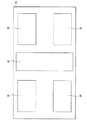
図1は、本発明の第1の実施の形態に係るマルチビーム半導体レーザの縦断面構造を表すものである。このマルチビーム半導体レーザは、例えば、プリンター用光源などとして用いられるものであり、例えば、一方の面に2本の突条部(ストライプ)11A,11Bが形成されたマルチビームの半導体レーザ素子10を有している。突条部11A,11Bの長さ(共振器長)は例えば400μmないし500μm程度である。半導体レーザ素子10は、突条部11A,11Bが形成された面を支持材(サブマウント)20に対向させたジャンクションダウンの状態で、はんだ層30により支持材20に接合されている。
<1. First Embodiment>
[Configuration of multi-beam semiconductor laser]
FIG. 1 shows a longitudinal sectional structure of a multi-beam semiconductor laser according to the first embodiment of the present invention. This multi-beam semiconductor laser is used, for example, as a light source for a printer. For example, a multi-beam
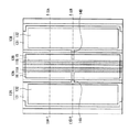
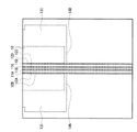
図2は、図1に示したマルチビーム半導体レーザを、突条部11A,11Bが形成された面の側から見た平面構成を表したものであり、図3(A)は図2のIIIA−IIIA線、図3(B)は図2のIIIB−IIIB線に沿った断面構成をそれぞれ表したものである。
FIG. 2 shows a planar configuration of the multi-beam semiconductor laser shown in FIG. 1 as viewed from the side on which the
この半導体レーザ素子10は、例えば、突条部11A,11Bが形成された面に、コンタクト電極12A,12Bと、パッド電極13A,13Bとを有している。コンタクト電極12A,12Bは、突条部11A,11Bの各々に設けられる一方、パッド電極113A,13Bは、突条部11A,11Bおよびコンタクト電極12A,12Bを回避して設けられている。コンタクト電極12Aとパッド電極13Aとは配線電極14Aにより接続され、コンタクト電極12Bとパッド電極13Bとは配線電極14Bにより接続されている。また、コンタクト電極12A,12Bの上には第1絶縁膜15が形成され、第1絶縁膜15の上には、金属よりなる熱伝導層16が設けられている。これにより、このマルチビーム半導体レーザでは、ジャンクションダウン組立の場合に放熱性を向上させることができるようになっている。
The
コンタクト電極12A,12Bは、例えば、積層方向の厚さ(以下、単に「厚さ」という。)が50nmのチタン(Ti)層と、厚さ100nmの白金(Pt)層と、厚さ300nmの金(Au)層とを順に積層した構成を有している。
The
パッド電極13A,13Bは、例えば、下部パッド電極131と、上部パッド電極132との積層構造を有している。下部パッド電極131は、例えば、厚さが50nmのチタン(Ti)層と、厚さ100nmの白金(Pt)層と、厚さ300nmの金(Au)層を順に積層した構成を有している。上部パッド電極132は、例えば、厚さ3μmの金めっき層により構成されている。
The
配線電極14A,14Bは、例えば、厚さが50nmのチタン(Ti)層と、厚さ100nmの白金(Pt)層と、厚さ300nmの金(Au)層とを順に積層した構成を有している。
The
第1絶縁膜15は、コンタクト電極12A,12Bがはんだ層30に直接接合されないようにすることにより、突条部11A,11Bにかかるはんだ接合応力を低減するためのものである。第1絶縁膜15の厚さは、例えば100nm程度であることが好ましい。薄いほうが放熱性を良くすることができるからである。第1絶縁膜15は、例えば、AlN,SiC,ダイヤモンド,BN,SiO2 およびSiNからなる群のうちの少なくとも1種により構成されていることが好ましい。
The first
熱伝導層16は、例えば、下部熱伝導層161と、上部熱伝導層162との積層構造を有している。下部熱伝導層161は、例えば、厚さが50nmのチタン(Ti)層と、厚さ100nmの白金(Pt)層と、厚さ300nmの金(Au)層を順に積層した構成を有している。上部熱伝導層162は、例えば、厚さ3μmの金めっき層により構成されている。
The heat
なお、コンタクト電極12A,12B、パッド電極13A,13Bの下部パッド電極131および配線電極14A,14Bは、同一の積層構造を有し、後述する製造工程においても同一工程において形成される。また、パッド電極13A,13Bの上部パッド電極132および熱伝導層16の上部熱伝導層162は、同一の金めっき層であり、後述する製造工程においても同一工程において形成される。
The
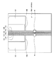
パッド電極13A,13Bおよび熱伝導層16の上には、更に別の金属層17(図2には図示せず、図13参照。)が形成されていてもよい。この金属層17は、金めっき層よりなる上部パッド電極132および上部熱伝導層162と、はんだ層30との合金化後の組成を一定にすることにより、融点のばらつきを防止し、はんだ層30のぬれ性を高めるためのものである。金属層17の構成材料や積層構造は、金めっき層よりなる上部パッド電極132および上部熱伝導層162と反応しないものであれば特に限定されないが、例えば、厚さが50nmのチタン(Ti)層と、厚さ100nmの白金(Pt)層と、厚さ300nmの金(Au)層とが順に積層された構成とすることができる。
On the
コンタクト電極12A,12Bは、突条部11A,11Bに対して左右対称の幅を有することが好ましい。コンタクト電極12A,12Bを設けることにより突条部11A,11Bにかかる応力を低減することができるからである。
The
第1絶縁膜15および熱伝導層16は、突条部11A,11Bおよびコンタクト電極12A,12Bよりも広い幅で、具体的には突条部11A,11Bおよびコンタクト電極12A,12Bの全部を覆うことができる幅で、形成されていることが好ましい。各突条部11A,11Bにかかる、熱伝導層16とはんだ層30との接合応力を、均一化すると共に低減することができるからである。
The first insulating
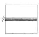
図4は、支持材20を、はんだ層30が形成された面の側から見た構成を表している。支持材20は、例えばAlNにより構成され、図示しないパッケージに配設されている。はんだ層30は、支持材20とパッド電極13A,13Bとの間、および支持材20と熱伝導層16との間に設けられ、例えば金(Au)−スズ(Sn)はんだにより構成されている。
FIG. 4 shows a configuration in which the
[半導体レーザ素子の構成例]
図5は、図1に示した半導体レーザ素子10の一例を表したものである。半導体レーザ素子10は、例えば、基板111の一面側に、n型クラッド層112,第1ガイド層113,活性層114,第2ガイド層115,第1p型クラッド層116,エッチングストップ層117,第2p型クラッド層118およびp側コンタクト層119がこの順に積層された構成を有している。基板111は、例えば、積層方向における厚さ(以下、単に厚さという)が110μmであり、ケイ素(Si)あるいはセレン(Se)などのn型不純物を添加したn型GaAsにより構成されている。
[Configuration example of semiconductor laser element]
FIG. 5 shows an example of the
n型クラッド層112は、例えば、厚さが2.0μmであり、ケイ素あるいはセレンなどのn型不純物を添加したn型Al0.5 In0.5 P混晶により構成されている。 For example, the n-type cladding layer 112 has a thickness of 2.0 μm and is made of an n-type Al 0.5 In 0.5 P mixed crystal to which an n-type impurity such as silicon or selenium is added.
第1ガイド層113は、例えば、厚さが120nmであり、Al0.3 Ga0.2 In0.5 P混晶により構成されている。第1ガイド層113は、不純物を含まなくてもよいし、または、ケイ素あるいはセレンなどのn型不純物が添加されていてもよい。 The first guide layer 113 has, for example, a thickness of 120 nm and is composed of an Al 0.3 Ga 0.2 In 0.5 P mixed crystal. The first guide layer 113 may not contain impurities, or may contain an n-type impurity such as silicon or selenium.
活性層114は、例えば、厚さが12nmであり、GaInP混晶により構成されている。活性層114に含まれるインジウム組成は、例えば0.2以上0.8以下であることが好ましい。更に、0.5程度であればより好ましい。基板111を構成するGaAsと格子整合させることができるからである。 The active layer 114 has a thickness of 12 nm, for example, and is composed of a GaInP mixed crystal. The indium composition contained in the active layer 114 is preferably 0.2 or more and 0.8 or less, for example. Furthermore, about 0.5 is more preferable. This is because lattice matching with GaAs constituting the substrate 111 can be achieved.
第2ガイド層115は、例えば、厚さが120nmであり、Al0.3 Ga0.2 In0.5 P混晶により構成されている。第2ガイド層115は、不純物を含まなくてもよいし、または、亜鉛(Zn)あるいはマグネシウム(Mg)などのp型不純物が添加されていてもよい。 The second guide layer 115 has, for example, a thickness of 120 nm and is composed of an Al 0.3 Ga 0.2 In 0.5 P mixed crystal. The second guide layer 115 may not contain impurities, or may be added with a p-type impurity such as zinc (Zn) or magnesium (Mg).
第1p型クラッド層116は、例えば、厚さが0.4μmであり、亜鉛またはマグネシウムなどのp型不純物を添加したp型Al0.5 In0.5 P混晶により構成されている。エッチングストップ層117は、後述する製造工程において第1p型クラッド層116の厚さのばらつきを抑制するためのものである。エッチングストップ層117は、例えば、厚さが15nmであり、亜鉛またはマグネシウムなどのp型不純物を添加したp型GaInPにより構成されている。第2p型クラッド層118は、例えば、厚さが1.6μmであり、亜鉛またはマグネシウムなどのp型不純物を添加したp型Al0.5 In0.5 P混晶により構成されている。p側コンタクト層119は、例えば、厚さが0.3μmであり、亜鉛またはマグネシウムなどのp型不純物を添加したp型GaAsにより構成されている。
For example, the first p-type cladding layer 116 has a thickness of 0.4 μm and is made of a p-type Al 0.5 In 0.5 P mixed crystal to which a p-type impurity such as zinc or magnesium is added. The etching stop layer 117 is for suppressing variation in the thickness of the first p-type cladding layer 116 in the manufacturing process described later. The etching stop layer 117 has a thickness of 15 nm, for example, and is made of p-type GaInP to which a p-type impurity such as zinc or magnesium is added. The second p-
このうち第2p型クラッド層118およびp側コンタクト層119は、細い帯状(図5においては紙面に対して垂直な方向に延長された帯状)に延長され、上述した突条部11A,11Bとされている。この突条部11A,11Bは、活性層114の電流注入領域を制限するためのものであり、活性層114の突条部11A,11Bに対応する部分が電流注入領域となっている。
Among these, the second p-
p側コンタクト層119の上には、例えば二酸化ケイ素(SiO2 )または窒化ケイ素(SiN)よりなる絶縁層120を間にして、上述したコンタクト電極12A,12Bが形成されている。一方、基板111の裏面には、n側電極124が形成されている。n側電極124は、例えば、例えばAuGe:Niおよび金(Au)を順次積層して熱処理により合金化した構造を有しており、基板111と電気的に接続されている。
On the p-side contact layer 119, the
なお、この半導体レーザ素子10では、例えば突条部11A,11Bの長さ方向において対向する一対の側面が共振器端面となっており、この一対の共振器端面に図示しない一対の反射鏡膜がそれぞれ形成されている。これら一対の反射鏡膜のうち一方の反射鏡膜の反射率は低くなるように、他方の反射鏡膜の反射率は高くなるようにそれぞれ調整されている。これにより、活性層114において発生した光は一対の反射鏡膜の間を往復して増幅され、一方の反射鏡膜からレーザビームとして出射するようになっている。
In the
[マルチビーム半導体レーザの製造方法]
このマルチビーム半導体レーザは、例えば、次のようにして製造することができる。
[Manufacturing method of multi-beam semiconductor laser]
This multi-beam semiconductor laser can be manufactured, for example, as follows.
図6は、図2ないし図5に示したマルチビーム半導体レーザの製造方法の流れを表したものであり、図7ないし図13は、この製造方法を工程順に表したものである。まず、例えば、GaNよりなる基板111を用意し、この基板111の表面に、例えばMOCVD(Metal Organic Chemical Vapor Deposition ;有機金属化学気相成長)法により、上述した厚さおよび材料よりなるn型クラッド層112,第1ガイド層113,活性層114,第2ガイド層115,第1p型クラッド層116,エッチングストップ層117,第2p型クラッド層118およびp側コンタクト層119を順に成長させる。
FIG. 6 shows the flow of the manufacturing method of the multi-beam semiconductor laser shown in FIGS. 2 to 5, and FIGS. 7 to 13 show this manufacturing method in the order of steps. First, for example, a substrate 111 made of GaN is prepared, and an n-type cladding made of the above-described thickness and material is formed on the surface of the substrate 111 by, for example, MOCVD (Metal Organic Chemical Vapor Deposition) method. The layer 112, the first guide layer 113, the active layer 114, the second guide layer 115, the first p-type cladding layer 116, the etching stop layer 117, the second p-
次いで、エッチングストップ層117を用いたエッチングを行い、p側コンタクト層119および第2p型クラッド層118の一部を選択的に除去し、図5および図7に示したように、細い帯状の突条部11A,11Bとする。続いて、図5に示したように、突条部11A,11Bの両側に、例えばCVD(Chemical Vapor Deposition ;化学気相成長)法により、上述した材料よりなる絶縁層123を形成し、この絶縁層123に、突条部11A,11Bに対応して開口部を設ける。
Next, etching using the etching stop layer 117 is performed to selectively remove a part of the p-side contact layer 119 and the second p-
そののち、図8に示したように、突条部11A,11Bの上に、上述した厚さおよび材料よりなるコンタクト電極12A,12Bを形成すると共に、突条部11A,11Bを回避してパッド電極13A,13Bの下部パッド電極131を形成し、コンタクト電極12A,12Bとパッド電極13A,13Bの下部パッド電極131とを、配線電極14A,14Bにより接続する(ステップS101)。
After that, as shown in FIG. 8, the
コンタクト電極12A,12B、パッド電極13A,13Bおよび配線電極14A,14Bを形成したのち、図9に示したように、全面に、上述した厚さおよび材料よりなる第1絶縁膜15を形成する(ステップS102)。
After the
第1絶縁膜15を形成したのち、図10に示したように、パッド電極13A,13B上の第1絶縁膜15を選択的に除去してコンタクトホール15Aを設ける(ステップS103)。これにより、コンタクト電極12A,12Bの上に第1絶縁膜15が形成される。
After forming the first insulating
第1絶縁膜15にコンタクトホール15Aを設けたのち、図11に示したように、第1絶縁膜15上に、上述した厚さおよび材料よりなる下部熱伝導層161を形成する(ステップS104)。
After providing the
下部熱伝導層161を形成したのち、図12に示したように、パッド電極13A,13Bの下部パッド電極131と、下部熱伝導層161との上に、上述した厚さの金めっき層よりなる上部パッド電極132と、上部熱伝導層162とをそれぞれ形成する(ステップS105)。これにより、突条部11A,11Bを回避してパッド電極13A,13Bが形成されると共に、第1絶縁膜15の上に熱伝導層16が形成される。
After the formation of the lower
上部パッド電極132および上部熱伝導層162を形成したのち、図13に示したように、上部パッド電極132および上部熱伝導層162の上に、上述した厚さおよび材料よりなる金属層17を形成する(ステップS106)。
After the formation of the
金属層17を形成したのち、基板111の裏面側を例えばラッピングおよびポリッシングして基板111の厚さを例えば100μm程度まで薄膜化し(ステップS107)、基板111の裏面に、上述した材料よりなるn側電極124を形成する(ステップS108)。そののち、基板111を所定の大きさに整え、対向する一対の共振器端面に図示しない反射鏡膜を形成する。
After the
続いて、上述した材料よりなる支持材20を用意し、図4に示したように、この支持材20の一面に、上述した材料よりなるはんだ層30を形成する。そののち、半導体レーザ素子10の突条部11A,11Bが形成された面を支持材20に対向させたジャンクションダウンの状態で、半導体レーザ素子10を、はんだ層30により支持材20に接合する。以上により、図1に示したマルチビーム半導体レーザが完成する。
Subsequently, the
このマルチビーム半導体レーザでは、n側電極124とコンタクト電極12A,12Bとの間に所定の電圧が印加されると、活性層114に電流が注入されて、電子−正孔再結合により発光が起こる。この光は、一対の反射鏡膜により反射され、その間を往復してレーザ発振を生じ、レーザビームとして外部に射出される。ここでは、コンタクト電極12A,12Bは、配線電極14A,14Bによりパッド電極13A,13Bに接続されると共に第1絶縁膜15で覆われているので、コンタクト電極12A,12Bは、はんだ層30に直接接合されることなく、パッド電極13A,13Bおよび配線電極14A,14Bを介して駆動される。また、第1絶縁膜15の上には、金属よりなる熱伝導層16が設けられているので、半導体レーザ素子10で発生した熱は、熱伝導層16を介してはんだ層30および支持材20へと放熱される。
In this multi-beam semiconductor laser, when a predetermined voltage is applied between the n-side electrode 124 and the
更に、コンタクト電極12A,12Bの上に第1絶縁膜15を設けることにより、コンタクト電極12A,12Bを設けることで突条部11A,11Bにかかる応力や、突条部11A,11Bにかかる熱伝導層16とはんだ層30との間の接合応力が低減される。よって、偏光特性や信頼性への影響が小さくなる。
Further, by providing the first insulating
特に、コンタクト電極12A,12Bを、突条部11A,11Bに対して左右対称の幅を有するようにしたので、コンタクト電極12A,12Bを設けることにより突条部11A,11Bにかかる応力が、更に低減される。
In particular, since the
このように本実施の形態では、コンタクト電極12A,12Bを、配線電極14A、14Bによりパッド電極13A,13Bに接続すると共に第1絶縁膜15で覆うようにしたので、コンタクト電極12A,12Bをはんだ層30に直接接合させることなく電気的接続が可能となる。また、第1絶縁膜15の上に、金属よりなる熱伝導層16を設けるようにしたので、この熱伝導層16とはんだ層30とを接合することにより、ジャンクションダウン組立の場合に放熱性を向上させることが可能となる。
As described above, in the present embodiment, the
更に、コンタクト電極12A,12Bの上に第1絶縁膜15を設けることにより、コンタクト電極12A,12Bを設けることで突条部11A,11Bにかかる応力や、各突条部11A,11Bにかかる熱伝導層16とはんだ層30との間の接合応力を低減することができる。よって、偏光特性や信頼性への影響を小さくすることが可能となる。
Further, by providing the first insulating
<2.第2の実施の形態>
[マルチビーム半導体レーザの構成]
図14は、本発明の第2の実施の形態に係るマルチビーム半導体レーザの縦断面構造を表したものである。このマルチビーム半導体レーザは、半導体レーザ素子10に4本の突条部11A,11B,11C,11Dが形成されていることにおいて、第1の実施の形態と異なるものである。よって、対応する構成要素には同一の符号を付して説明する。
<2. Second Embodiment>
[Configuration of multi-beam semiconductor laser]
FIG. 14 shows a longitudinal sectional structure of a multi-beam semiconductor laser according to the second embodiment of the present invention. This multi-beam semiconductor laser is different from the first embodiment in that four
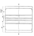
図15は、図14に示したマルチビーム半導体レーザを、突条部11A〜11Dが形成された面の側から見た平面構成を表したものであり、図16(A)は図15のXVIA−XVIA線、図16(B)は図15のXVIB−XVIB線、図16(C)は図15のXVIC−XVIC線に沿った断面構成をそれぞれ表したものである。
FIG. 15 shows a planar configuration of the multi-beam semiconductor laser shown in FIG. 14 as viewed from the side on which the
半導体レーザ素子10および突条部11A〜11Dについては、第1の実施の形態と同様に構成されている。
The
半導体レーザ素子10の突条部11A〜11Dが形成された面には、四つのコンタクト電極12A,12B,12C,12Dおよび四つのパッド電極13A,13B,13C,13Dが設けられている。コンタクト電極12A〜12Dおよびパッド電極13A〜13Dは、配線電極14A,14B,14C,14Dによりそれぞれ接続されている。
Four
コンタクト電極12A〜12Dは、第1の実施の形態と同様に、突条部11A〜11Dに対して左右対称の幅を有することが好ましい。コンタクト電極12A〜12Dを設けることにより突条部11A〜11Dにかかる応力を低減することができるからである。
As in the first embodiment, the
配線電極14Bは、コンタクト電極12Bとパッド電極13Bとを、コンタクト電極12Aを越えて接続しており、配線電極14Bとコンタクト電極12Aとの間は、第2絶縁膜18により絶縁されている。配線電極14Cは、コンタクト電極12Cとパッド電極12Cとを、コンタクト電極12Dを越えて接続しており、配線電極14Cとコンタクト電極12Dとの間も、第2絶縁膜18により絶縁されている。これにより、本実施の形態では、半導体レーザ素子10に4本の突条部11A〜11Dが形成されている場合も、コンタクト電極12A〜12Dをはんだ層30に直接接合させることなく、配線電極14A〜14Dによりパッド電極13A〜13Dに接続することができるようになっている。
The
第1絶縁膜15、熱伝導層16、金属層17は、第1の実施の形態と同様に構成されている。
The first insulating
第2絶縁膜18は、例えば、厚さが100nm程度であることが好ましい。薄いほうが放熱性を良くすることができるからである。また、第2絶縁膜18は、例えば、AlN,SiC,ダイヤモンド,BN,SiO2 およびSiNからなる群のうちの少なくとも1種により構成されていることが好ましい。
The second insulating
図17は、支持材20を、はんだ層30が形成された面の側から見た構成を表している。はんだ層30は、支持材20とパッド電極13A〜13Dとの間、および支持材20と熱伝導層16との間に設けられている。
FIG. 17 illustrates a configuration in which the
[マルチビーム半導体レーザの製造方法]
このマルチビーム半導体レーザは、例えば、次のようにして製造することができる。
[Manufacturing method of multi-beam semiconductor laser]
This multi-beam semiconductor laser can be manufactured, for example, as follows.
図18は、図15ないし図17に示したマルチビーム半導体レーザの製造方法の流れを表したものであり、図19ないし図28は、この製造方法を工程順に表したものである。まず、図19に示したように、第1の実施の形態と同様にして、図5および図7に示した工程により、4本の突条部11A〜11Dを有する半導体レーザ素子10を形成する。
FIG. 18 shows the flow of the manufacturing method of the multi-beam semiconductor laser shown in FIGS. 15 to 17, and FIGS. 19 to 28 show this manufacturing method in the order of steps. First, as shown in FIG. 19, as in the first embodiment, the
次いで、図20に示したように、突条部11A〜11Dの上に、上述した厚さおよび材料よりなるコンタクト電極12A〜12Dを形成すると共に、突条部11A〜11Dを回避してパッド電極13A,13Dの下部パッド電極131を形成し、コンタクト電極12A,12Dとパッド電極13A,13Bの下部パッド電極131とを、配線電極14A,14Dにより接続する(ステップS201)。
Next, as shown in FIG. 20, the
続いて、図21に示したように、全面に、上述した厚さおよび材料よりなる第2絶縁膜18を形成する(ステップS202)。
Subsequently, as shown in FIG. 21, the second insulating
そののち、図22に示したように、第2絶縁膜18を選択的に除去してコンタクトホール18Aを設ける(ステップS203)。これにより、コンタクト電極12A,12Dの上の配線電極14B,14C形成予定位置に第2絶縁膜18が形成される。
After that, as shown in FIG. 22, the second insulating
第2絶縁膜18にコンタクトホール18Aを設けたのち、図23に示したように、突条部11A〜11Dを回避してパッド電極13B,13Cの下部パッド電極131を形成し、コンタクト電極12B,12Cとパッド電極13B,13Cの下部パッド電極131とを、配線電極14B,14Cにより接続する(ステップS204)。その際、配線電極14B,14Cを第2絶縁膜18上に形成することにより、配線電極14B,14Cとコンタクト電極14A,14Dとの間を第2絶縁膜18で絶縁する。
After providing the contact hole 18A in the second insulating
続いて、図24に示したように、全面に、上述した厚さおよび材料よりなる第1絶縁膜15を形成する(ステップS205)。
Subsequently, as shown in FIG. 24, the first insulating
そののち、図25に示したように、パッド電極13A〜13D上の第1絶縁膜15を選択的に除去してコンタクトホール15Aを設ける(ステップS206)。これにより、コンタクト電極12A〜12Dの上に第1絶縁膜15が形成される。
Thereafter, as shown in FIG. 25, the first insulating
第1絶縁膜15を形成したのち、図26に示したように、第1絶縁膜15上に、上述した厚さおよび材料よりなる下部熱伝導層161を形成する(ステップS207)。
After forming the first insulating
下部熱伝導層161を形成したのち、図27に示したように、パッド電極13A〜13Dの下部パッド電極131と、下部熱伝導層161との上に、上述した厚さの金めっき層よりなる上部パッド電極132と、上部熱伝導層162とをそれぞれ形成する(ステップS208)。これにより、突条部11A〜11Bを回避してパッド電極13A〜13Dが形成されると共に、第1絶縁膜15の上に熱伝導層16が形成される。
After the formation of the lower
上部パッド電極132および上部熱伝導層162を形成したのち、図28に示したように、上部パッド電極132および上部熱伝導層162の上に、上述した厚さおよび材料よりなる金属層17を形成する(ステップS209)。
After the formation of the
金属層17を形成したのち、基板111の裏面側を例えばラッピングおよびポリッシングして基板111の厚さを例えば100μm程度まで薄膜化し(ステップS210)、基板111の裏面に、上述した材料よりなるn側電極124を形成する(ステップS211)。そののち、基板111を所定の大きさに整え、対向する一対の共振器端面に図示しない反射鏡膜を形成する。
After the
続いて、上述した材料よりなる支持材20を用意し、図17に示したように、この支持材20の一面に、上述した材料よりなるはんだ層30を形成する。そののち、半導体レーザ素子10の突条部11A,11Bが形成された面を支持材20に対向させたジャンクションダウンの状態で、半導体レーザ素子10を、はんだ層30により支持材20に接合する。以上により、図14に示したマルチビーム半導体レーザが完成する。
Subsequently, the
このマルチビーム半導体レーザでは、n側電極124とコンタクト電極12A〜12Dとの間に所定の電圧が印加されると、第1の実施の形態と同様にしてレーザ発振が起こる。ここでは、配線電極14B,14Cとコンタクト電極12A,12Dとの間は第2絶縁膜18により絶縁されているので、半導体レーザ素子10に4本の突条部11A〜11Dが形成されている場合も、コンタクト電極12A〜12Dは、はんだ層30に直接接合されることなく、パッド電極13A〜13Dおよび配線電極14A〜14Dを介して駆動される。
In this multi-beam semiconductor laser, when a predetermined voltage is applied between the n-side electrode 124 and the
また、第1絶縁膜15の上には、金属よりなる熱伝導層16が設けられているので、半導体レーザ素子10で発生した熱は、熱伝導層16を介してはんだ層30および支持材20へと放熱される。
In addition, since the heat
更に、コンタクト電極12A〜12Dの上に第1絶縁膜15を設けることにより、コンタクト電極12A〜12Dを設けることで突条部11A〜11Dにかかる応力や、突条部11A〜11Dにかかる熱伝導層16とはんだ層30との間の接合応力が低減される。よって、偏光特性や信頼性への影響が小さくなる。
Further, by providing the first insulating
特に、コンタクト電極12A〜12Dを、突条部11A〜11Dに対して左右対称の幅を有するようにしたので、コンタクト電極12A〜12Dを設けることにより突条部11A〜11Dにかかる応力が、更に低減される。
In particular, since the
このように本実施の形態では、配線電極14B,14Cとコンタクト電極12A,12Dとの間を第2絶縁膜18により絶縁するようにしたので、半導体レーザ素子10に4本の突条部11A〜11Dが形成されている場合も、コンタクト電極12A〜12Dをはんだ層30に直接接合させることなく電気的接続が可能となる。また、第1絶縁膜15の上に、金属よりなる熱伝導層16を設けるようにしたので、この熱伝導層16とはんだ層30とを接合することにより、ジャンクションダウン組立の場合に放熱性を向上させることが可能となる。
As described above, in the present embodiment, the
更に、コンタクト電極12A,12Bの上に第1絶縁膜15を設けることにより、コンタクト電極12A,12Bを設けることで突条部11A,11Bにかかる応力や、各突条部11A,11Bにかかる熱伝導層16とはんだ層30との間の接合応力を低減することができる。よって、偏光特性や信頼性への影響を小さくすることが可能となる。
Further, by providing the first insulating
<3.第3の実施の形態>
[マルチビーム半導体レーザの構成]
図29は、本発明の第2の実施の形態に係るマルチビーム半導体レーザを、突条部11A〜11Dが形成された面の側から見た平面構成を表したものであり、図30(A)は図29のXXXA−XXXA線、図30(B)は図29のXXXB−XXXB線、図30(C)は図29のXXXC−XXXC線に沿った断面構成をそれぞれ表したものである。このマルチビーム半導体レーザは、配線電極14B,14Cが、半導体レーザ素子10の高抵抗化領域125に形成されていることにおいて、第2の実施の形態と異なるものである。よって、対応する構成要素には同一の符号を付して説明する。
<3. Third Embodiment>
[Configuration of multi-beam semiconductor laser]
FIG. 29 illustrates a planar configuration of the multi-beam semiconductor laser according to the second embodiment of the present invention as viewed from the side on which the
半導体レーザ素子10には、イオン注入、およびp側コンタクト層119を除去することのうち少なくとも一方が行われた高抵抗化領域125が形成されていることを除いては、第1の実施の形態と同様に形成されている。高抵抗化領域125は、例えば、リア端面に設けられていることが好ましい。
The
突条部11A〜11D、コンタクト電極12A〜12D、パッド電極13A〜13Dについては、第1の実施の形態と同様に構成されている。
The
コンタクト電極12A〜12Dは、第1の実施の形態と同様に、突条部11A〜11Dに対して左右対称の幅を有することが好ましい。コンタクト電極12A〜12Dを設けることにより突条部11A〜11Dにかかる応力を低減することができるからである。
As in the first embodiment, the
配線電極14Bは、コンタクト電極12Bとパッド電極13Bとを、コンタクト電極12Aを越えて接続し、配線電極14Cは、コンタクト電極12Cとパッド電極12Cとを、コンタクト電極12Dを越えて接続している。配線電極14B,14Cは、半導体レーザ素子10の高抵抗化領域125に設けられている。これにより、本実施の形態では、半導体レーザ素子10に4本の突条部11A〜11Dが形成されている場合も、コンタクト電極12A〜12Dをはんだ層30に直接接合させることなく、配線電極14A〜14Dによりパッド電極13A〜13Dに接続することができるようになっている。また、第2絶縁膜18は不要となり、製造工程を簡素化することも可能となる。
The
第1絶縁膜15、熱伝導層16、金属層17は、第1の実施の形態と同様に構成されている。支持材20およびはんだ層30は、第2の実施の形態と同様に構成されている。
The first insulating
[マルチビーム半導体レーザの製造方法]
このマルチビーム半導体レーザは、例えば、次のようにして製造することができる。
[Manufacturing method of multi-beam semiconductor laser]
This multi-beam semiconductor laser can be manufactured, for example, as follows.
図31は、図29および図30に示したマルチビーム半導体レーザの製造方法の流れを表したものであり、図32ないし図39は、この製造方法を工程順に表したものである。まず、図32に示したように、第1の実施の形態と同様にして、図5および図7に示した工程により、4本の突条部11A〜11Dを有する半導体レーザ素子10を形成する。その際、リア端面に、イオン注入、およびp側コンタクト層119を除去することのうち少なくとも一方を行うことにより高抵抗化領域125を形成する。
FIG. 31 shows the flow of the manufacturing method of the multi-beam semiconductor laser shown in FIGS. 29 and 30. FIGS. 32 to 39 show this manufacturing method in the order of steps. First, as shown in FIG. 32, similarly to the first embodiment, the
次いで、図33に示したように、突条部11A〜11Dの上に、上述した厚さおよび材料よりなるコンタクト電極12A〜12Dを形成すると共に、突条部11A〜11Dを回避してパッド電極13A,13Dの下部パッド電極131を形成し、コンタクト電極12A,12Dとパッド電極13A,13Dの下部パッド電極131とを、配線電極14A,14Dにより接続する(ステップS301)。
Next, as shown in FIG. 33, the
続いて、図34に示したように、突条部11A〜11Dを回避してパッド電極13B,13Cの下部パッド電極131を形成し、コンタクト電極12B,12Cとパッド電極13B,13Cの下部パッド電極131とを、配線電極14B,14Cにより接続する(ステップS302)。その際、配線電極14B,14Cを、半導体レーザ素子10のリア端面の高抵抗化領域125に形成する。
Subsequently, as shown in FIG. 34, the
そののち、図35に示したように、全面に、上述した厚さおよび材料よりなる第1絶縁膜15を形成する(ステップS303)。
After that, as shown in FIG. 35, the first insulating
そののち、図36に示したように、パッド電極13A〜13D上の第1絶縁膜15を選択的に除去してコンタクトホール15Aを設ける(ステップS304)。これにより、コンタクト電極12A〜12Dの上に第1絶縁膜15が形成される。
Thereafter, as shown in FIG. 36, the first insulating
第1絶縁膜15を形成したのち、図37に示したように、第1絶縁膜15上に、上述した厚さおよび材料よりなる下部熱伝導層161を形成する(ステップS305)。
After forming the first insulating
下部熱伝導層161を形成したのち、図38に示したように、パッド電極13A〜13Dの下部パッド電極131と、下部熱伝導層161との上に、上述した厚さの金めっき層よりなる上部パッド電極132と、上部熱伝導層162とをそれぞれ形成する(ステップS306)。これにより、突条部11A〜11Bを回避してパッド電極13A〜13Dが形成されると共に、第1絶縁膜15の上に熱伝導層16が形成される。
After the formation of the lower thermal
上部パッド電極132および上部熱伝導層162を形成したのち、図39に示したように、上部パッド電極132および上部熱伝導層162の上に、上述した厚さおよび材料よりなる金属層17を形成する(ステップS307)。
After the formation of the
金属層17を形成したのち、基板111の裏面側を例えばラッピングおよびポリッシングして基板111の厚さを例えば100μm程度まで薄膜化し(ステップS308)、基板111の裏面に、上述した材料よりなるn側電極124を形成する(ステップS309)。そののち、基板111を所定の大きさに整え、対向する一対の共振器端面に図示しない反射鏡膜を形成する。
After the
続いて、上述した材料よりなる支持材20を用意し、図17に示したように、この支持材20の一面に、上述した材料よりなるはんだ層30を形成する。そののち、半導体レーザ素子10の突条部11A,11Bが形成された面を支持材20に対向させたジャンクションダウンの状態で、半導体レーザ素子10を、はんだ層30により支持材20に接合する。以上により、本実施の形態のマルチビーム半導体レーザが完成する。
Subsequently, the
このマルチビーム半導体レーザでは、n側電極124とコンタクト電極12A〜12Dとの間に所定の電圧が印加されると、第1の実施の形態と同様にしてレーザ発振が起こる。ここでは、配線電極14B,14Cが、半導体レーザ素子10の高抵抗化領域125に形成されているので、半導体レーザ素子10に4本の突条部11A〜11Dが形成されている場合も、コンタクト電極12A〜12Dは、はんだ層30に直接接合されることなく、パッド電極13A〜13Dおよび配線電極14A〜14Dを介して駆動される。
In this multi-beam semiconductor laser, when a predetermined voltage is applied between the n-side electrode 124 and the
また、第1絶縁膜15の上には、金属よりなる熱伝導層16が設けられているので、半導体レーザ素子10で発生した熱は、熱伝導層16を介してはんだ層30および支持材20へと放熱される。
In addition, since the heat
更に、コンタクト電極12A〜12Dの上に第1絶縁膜15を設けることにより、コンタクト電極12A〜12Dを設けることで突条部11A〜11Dにかかる応力や、突条部11A〜11Dにかかる熱伝導層16とはんだ層30との間の接合応力が低減される。よって、偏光特性や信頼性への影響が小さくなる。
Further, by providing the first insulating
特に、コンタクト電極12A〜12Dを、突条部11A〜11Dに対して左右対称の幅を有するようにしたので、コンタクト電極12A〜12Dを設けることにより突条部11A〜11Dにかかる応力が、更に低減される。
In particular, since the
このように本実施の形態では、配線電極14B,14Cを、半導体レーザ素子10の高抵抗化領域125に形成するようにしたので、半導体レーザ素子10に4本の突条部11A〜11Dが形成されている場合も、コンタクト電極12A〜12Dをはんだ層30に直接接合させることなく電気的接続が可能となる。また、第1絶縁膜15の上に、金属よりなる熱伝導層16を設けるようにしたので、この熱伝導層16とはんだ層30とを接合することにより、ジャンクションダウン組立の場合に放熱性を向上させることが可能となる。
As described above, in the present embodiment, since the
更に、コンタクト電極12A,12Bの上に第1絶縁膜15を設けることにより、コンタクト電極12A,12Bを設けることで突条部11A,11Bにかかる応力や、各突条部11A,11Bにかかる熱伝導層16とはんだ層30との間の接合応力を低減することができる。よって、偏光特性や信頼性への影響を小さくすることが可能となる。
Further, by providing the first insulating
以上、実施の形態を挙げて本発明を説明したが、本発明は上記実施の形態に限定されるものではなく、種々変形が可能である。例えば、上記実施の形態では、半導体レーザ素子10が2本または4本の突条部11A〜11Dを有する場合について説明したが、突条部の数すなわちビームの数は2本、4本などの偶数に限らず、3本または5本などの奇数であってもよい。また、突条部11A〜11Dの数とパッド電極13A〜13Dの数とは必ずしも同じである必要はない。例えば、突条部の数がパッド電極よりも少ない場合には、どのコンタクト電極にも接続されていないダミーのパッド電極を設けるようにしてもよい。また、パッド電極の数が突条部よりも多い場合には、一つのコンタクト電極を二つ以上のパッド電極に接続するようにしてもよい。
While the present invention has been described with reference to the embodiment, the present invention is not limited to the above embodiment, and various modifications can be made. For example, in the above embodiment, the case where the
また、上記実施の形態では、マルチビーム半導体レーザを例として説明したが、本発明は多波長レーザにも適用可能である。 In the above embodiment, a multi-beam semiconductor laser has been described as an example. However, the present invention can also be applied to a multi-wavelength laser.
更に、上記実施の形態では、一つのコンタクト電極と一つのパッド電極とを一本の配線電極で接続する場合について説明したが、配線電極は多数でもよい。 Furthermore, although the case where one contact electrode and one pad electrode are connected by one wiring electrode has been described in the above embodiment, the number of wiring electrodes may be large.
加えて、例えば、上記実施の形態において説明した各層の材料および厚さ、または成膜方法および成膜条件などは限定されるものではなく、他の材料および厚さとしてもよく、または他の成膜方法および成膜条件としてもよい。例えば、上記実施の形態では、バッファ層112ないしp側コンタクト層122をMOCVD法により形成する場合について説明したが、MOVPE法等の他の有機金属気相成長法により形成してもよく、あるいは、MBE(Molecular Beam Epitaxy;分子線エピタキシー)法等を用いてもよい。 In addition, for example, the material and thickness of each layer described in the above embodiment, the film formation method and the film formation conditions are not limited, and other materials and thicknesses may be used. It is good also as a film | membrane method and film-forming conditions. For example, in the above embodiment, the case where the buffer layer 112 or the p-side contact layer 122 is formed by the MOCVD method has been described. However, the buffer layer 112 or the p-side contact layer 122 may be formed by another metal organic chemical vapor deposition method such as the MOVPE method, An MBE (Molecular Beam Epitaxy) method or the like may be used.
更にまた、例えば、上記実施の形態では、半導体レーザ素子の構成を具体的に挙げて説明したが、全ての層を備える必要はなく、また、他の層を更に備えていてもよい。 Furthermore, for example, in the above-described embodiment, the configuration of the semiconductor laser element has been specifically described, but it is not necessary to include all layers, and other layers may be further included.
加えてまた、本発明は、AlGaInP系の赤色レーザに限らず、より高出力のものや、他の発振波長または他の材料系のものにも適用可能である。 In addition, the present invention is not limited to AlGaInP red lasers, but can be applied to higher output lasers, other oscillation wavelengths, or other material systems.
10…半導体レーザ素子、11A〜11D…突条部、12A〜12D…コンタクト電極、13A〜13D…パッド電極、14A〜14D…配線電極、15…第1絶縁膜、16…熱伝導層、17…金属層、18…第2絶縁膜、124…n側電極、125…高抵抗化領域。
DESCRIPTION OF
Claims (8)
前記複数の突条部の各々に設けられたコンタクト電極と、
前記半導体レーザ素子の前記複数の突条部が形成された面に、前記複数の突条部を回避して設けられた複数のパッド電極と、
前記コンタクト電極を前記複数のパッド電極のうちの少なくとも一つに接続する配線電極と、
前記コンタクト電極の上に形成された第1絶縁膜と、
前記第1絶縁膜の上に設けられた金属よりなる熱伝導層と
を備えたマルチビーム半導体レーザ。 A semiconductor laser element formed with a plurality of protrusions;
A contact electrode provided on each of the plurality of protrusions;
A plurality of pad electrodes provided to avoid the plurality of protrusions on the surface of the semiconductor laser element on which the plurality of protrusions are formed;
A wiring electrode connecting the contact electrode to at least one of the plurality of pad electrodes;
A first insulating film formed on the contact electrode;
A multi-beam semiconductor laser comprising: a heat conductive layer made of metal provided on the first insulating film.
請求項1記載のマルチビーム半導体レーザ。 The first insulating film, AlN, SiC, diamond, BN, multi-beam semiconductor laser according to claim 1, characterized in that it is constituted by at least one selected from the group consisting of SiO 2 and SiN.
請求項1または2記載のマルチビーム半導体レーザ。 The multi-beam semiconductor laser according to claim 1, wherein the contact electrode has a symmetrical width with respect to the protrusion.
請求項1ないし3のいずれか1項に記載のマルチビーム半導体レーザ。 The wiring electrode connects the contact electrode and at least one of the plurality of pad electrodes beyond another contact electrode, and second insulation is provided between the other contact electrode and the wiring electrode. The multi-beam semiconductor laser according to any one of claims 1 to 3, wherein the multi-beam semiconductor laser is insulated by a film.
請求項4記載のマルチビーム半導体レーザ。 5. The multi-beam semiconductor laser according to claim 4, wherein the second insulating film is made of at least one selected from the group consisting of AlN, SiC, diamond, BN, SiO 2 and SiN.
請求項1ないし3のいずれか1項に記載のマルチビーム半導体レーザ。 The wiring electrode connects the contact electrode and at least one of the plurality of pad electrodes over other contact electrodes, and the wiring electrode is formed in a high resistance region of the semiconductor laser element. The multi-beam semiconductor laser according to any one of claims 1 to 3.
請求項6記載のマルチビーム半導体レーザ。 The multi-beam semiconductor laser according to claim 6, wherein the high resistance region is a region where at least one of ion implantation and removal of the p-side contact layer is performed.
前記支持材と前記パッド電極との間、および前記支持材と前記熱伝導層との間に設けられたはんだ層と
を備えた請求項1ないし7のいずれか1項に記載のマルチビーム半導体レーザ。 A support material;
The multi-beam semiconductor laser according to claim 1, further comprising: a solder layer provided between the support material and the pad electrode and between the support material and the heat conductive layer. .
Priority Applications (3)
| Application Number | Priority Date | Filing Date | Title |
|---|---|---|---|
| JP2008214701A JP4697488B2 (en) | 2008-08-22 | 2008-08-22 | Multi-beam semiconductor laser |
| US12/458,565 US8121168B2 (en) | 2008-08-22 | 2009-07-16 | Multibeam laser diode |
| CN200910166649XA CN101656399B (en) | 2008-08-22 | 2009-08-24 | Multibeam laser diode |
Applications Claiming Priority (1)
| Application Number | Priority Date | Filing Date | Title |
|---|---|---|---|
| JP2008214701A JP4697488B2 (en) | 2008-08-22 | 2008-08-22 | Multi-beam semiconductor laser |
Publications (2)
| Publication Number | Publication Date |
|---|---|
| JP2010050362A true JP2010050362A (en) | 2010-03-04 |
| JP4697488B2 JP4697488B2 (en) | 2011-06-08 |
Family
ID=41696349
Family Applications (1)
| Application Number | Title | Priority Date | Filing Date |
|---|---|---|---|
| JP2008214701A Expired - Fee Related JP4697488B2 (en) | 2008-08-22 | 2008-08-22 | Multi-beam semiconductor laser |
Country Status (3)
| Country | Link |
|---|---|
| US (1) | US8121168B2 (en) |
| JP (1) | JP4697488B2 (en) |
| CN (1) | CN101656399B (en) |
Families Citing this family (4)
| Publication number | Priority date | Publication date | Assignee | Title |
|---|---|---|---|---|
| JP5380135B2 (en) * | 2009-04-03 | 2014-01-08 | 日本オクラロ株式会社 | Multi-beam semiconductor laser device |
| US10833474B2 (en) * | 2017-08-02 | 2020-11-10 | Nlight, Inc. | CTE-matched silicon-carbide submount with high thermal conductivity contacts |
| CN107910747A (en) * | 2017-12-12 | 2018-04-13 | 中国科学院苏州纳米技术与纳米仿生研究所 | More ridge type semiconductor lasers and preparation method thereof |
| CN110808529A (en) * | 2018-08-06 | 2020-02-18 | 潍坊华光光电子有限公司 | Semiconductor laser with optimized heat conduction and preparation method thereof |
Citations (15)
| Publication number | Priority date | Publication date | Assignee | Title |
|---|---|---|---|---|
| JPS58122472U (en) * | 1982-02-15 | 1983-08-20 | 沖電気工業株式会社 | laser diode array |
| JPS63199479A (en) * | 1987-02-16 | 1988-08-17 | Nec Corp | Semiconductor laser array device |
| JPH07147453A (en) * | 1993-11-25 | 1995-06-06 | Fuji Xerox Co Ltd | Semiconductor laser device |
| JPH11135893A (en) * | 1997-08-29 | 1999-05-21 | Xerox Corp | Edge-emitting laser |
| JPH11145567A (en) * | 1997-09-26 | 1999-05-28 | Xerox Corp | Semiconductor laser array |
| JP2000269601A (en) * | 1999-03-18 | 2000-09-29 | Sony Corp | Semiconductor light emitting device and its manufacture |
| JP2002344084A (en) * | 2001-05-11 | 2002-11-29 | Sony Corp | Multi-beam semiconductor light-emitting device and manufacturing method therefor |
| JP2004087866A (en) * | 2002-08-28 | 2004-03-18 | Hitachi Ltd | Semiconductor optical element and package therewith, and optical module |
| JP2004140141A (en) * | 2002-10-17 | 2004-05-13 | Mitsubishi Electric Corp | Semiconductor laser |
| JP2005045146A (en) * | 2003-07-25 | 2005-02-17 | Sony Corp | Multi-beam semiconductor light emitting device and manufacturing method thereof |
| JP2005101483A (en) * | 2002-11-25 | 2005-04-14 | Nichia Chem Ind Ltd | Ridge waveguide type semiconductor laser |
| JP2006024665A (en) * | 2004-07-07 | 2006-01-26 | Ricoh Printing Systems Ltd | Array type semiconductor laser device |
| JP2006278576A (en) * | 2005-03-28 | 2006-10-12 | Sanyo Electric Co Ltd | Semiconductor laser device, its manufacturing method, and optical pickup device |
| JP2007048810A (en) * | 2005-08-08 | 2007-02-22 | Sony Corp | Semiconductor laser |
| JP2007173402A (en) * | 2005-12-20 | 2007-07-05 | Matsushita Electric Ind Co Ltd | Semiconductor laser device |
Family Cites Families (2)
| Publication number | Priority date | Publication date | Assignee | Title |
|---|---|---|---|---|
| FR2821166B1 (en) * | 2001-02-19 | 2004-06-18 | Teem Photonics | COUPLING COMPONENT PRODUCED IN INTEGRATED OPTICS, CAPABLE OF ADAPTING A LIGHT SOURCE TO A GUIDED OPTICAL ELEMENT AND POWER LASER COMPRISING SAME |
| TWI303909B (en) * | 2002-11-25 | 2008-12-01 | Nichia Corp | Ridge waveguide semiconductor laser diode |
-
2008
- 2008-08-22 JP JP2008214701A patent/JP4697488B2/en not_active Expired - Fee Related
-
2009
- 2009-07-16 US US12/458,565 patent/US8121168B2/en not_active Expired - Fee Related
- 2009-08-24 CN CN200910166649XA patent/CN101656399B/en not_active Expired - Fee Related
Patent Citations (15)
| Publication number | Priority date | Publication date | Assignee | Title |
|---|---|---|---|---|
| JPS58122472U (en) * | 1982-02-15 | 1983-08-20 | 沖電気工業株式会社 | laser diode array |
| JPS63199479A (en) * | 1987-02-16 | 1988-08-17 | Nec Corp | Semiconductor laser array device |
| JPH07147453A (en) * | 1993-11-25 | 1995-06-06 | Fuji Xerox Co Ltd | Semiconductor laser device |
| JPH11135893A (en) * | 1997-08-29 | 1999-05-21 | Xerox Corp | Edge-emitting laser |
| JPH11145567A (en) * | 1997-09-26 | 1999-05-28 | Xerox Corp | Semiconductor laser array |
| JP2000269601A (en) * | 1999-03-18 | 2000-09-29 | Sony Corp | Semiconductor light emitting device and its manufacture |
| JP2002344084A (en) * | 2001-05-11 | 2002-11-29 | Sony Corp | Multi-beam semiconductor light-emitting device and manufacturing method therefor |
| JP2004087866A (en) * | 2002-08-28 | 2004-03-18 | Hitachi Ltd | Semiconductor optical element and package therewith, and optical module |
| JP2004140141A (en) * | 2002-10-17 | 2004-05-13 | Mitsubishi Electric Corp | Semiconductor laser |
| JP2005101483A (en) * | 2002-11-25 | 2005-04-14 | Nichia Chem Ind Ltd | Ridge waveguide type semiconductor laser |
| JP2005045146A (en) * | 2003-07-25 | 2005-02-17 | Sony Corp | Multi-beam semiconductor light emitting device and manufacturing method thereof |
| JP2006024665A (en) * | 2004-07-07 | 2006-01-26 | Ricoh Printing Systems Ltd | Array type semiconductor laser device |
| JP2006278576A (en) * | 2005-03-28 | 2006-10-12 | Sanyo Electric Co Ltd | Semiconductor laser device, its manufacturing method, and optical pickup device |
| JP2007048810A (en) * | 2005-08-08 | 2007-02-22 | Sony Corp | Semiconductor laser |
| JP2007173402A (en) * | 2005-12-20 | 2007-07-05 | Matsushita Electric Ind Co Ltd | Semiconductor laser device |
Also Published As
| Publication number | Publication date |
|---|---|
| JP4697488B2 (en) | 2011-06-08 |
| CN101656399B (en) | 2011-12-21 |
| US8121168B2 (en) | 2012-02-21 |
| US20100046563A1 (en) | 2010-02-25 |
| CN101656399A (en) | 2010-02-24 |
Similar Documents
| Publication | Publication Date | Title |
|---|---|---|
| JP4352337B2 (en) | Semiconductor laser and semiconductor laser device | |
| US11626707B2 (en) | Semiconductor laser diode | |
| JP5465514B2 (en) | Optical semiconductor device | |
| US11923662B2 (en) | Edge-emitting laser bar | |
| JP4966283B2 (en) | Semiconductor laser device and manufacturing method thereof | |
| JP2008288527A (en) | Laser light-emitting device | |
| JP7332623B2 (en) | Semiconductor laser device | |
| JP4697488B2 (en) | Multi-beam semiconductor laser | |
| JP4583058B2 (en) | Semiconductor laser element | |
| US7653110B2 (en) | Semiconductor laser apparatus and method for mounting semiconductor laser apparatus | |
| JP2002016313A (en) | Nitride semiconductor laser element and its manufacturing method | |
| JP4935676B2 (en) | Semiconductor light emitting device | |
| JP4737387B2 (en) | Semiconductor laser element | |
| JP2005101483A (en) | Ridge waveguide type semiconductor laser | |
| JPH07335975A (en) | Gallium nitride series compound semiconductor laser element | |
| JP2007173402A (en) | Semiconductor laser device | |
| WO2022201771A1 (en) | Semiconductor laser | |
| JP2010098001A (en) | Semiconductor laser device and method of manufacturing the same | |
| JPH10200213A (en) | Gallium nitride semiconductor laser | |
| WO2023140224A1 (en) | Semiconductor laser device and method for manufacturing semiconductor laser element | |
| JP2013143435A (en) | Semiconductor light-emitting element and manufacturing method of the same |
Legal Events
| Date | Code | Title | Description |
|---|---|---|---|
| A977 | Report on retrieval |
Free format text: JAPANESE INTERMEDIATE CODE: A971007 Effective date: 20100607 |
|
| A131 | Notification of reasons for refusal |
Free format text: JAPANESE INTERMEDIATE CODE: A131 Effective date: 20100615 |
|
| A521 | Request for written amendment filed |
Free format text: JAPANESE INTERMEDIATE CODE: A523 Effective date: 20100812 |
|
| TRDD | Decision of grant or rejection written | ||
| A01 | Written decision to grant a patent or to grant a registration (utility model) |
Free format text: JAPANESE INTERMEDIATE CODE: A01 Effective date: 20110202 |
|
| A61 | First payment of annual fees (during grant procedure) |
Free format text: JAPANESE INTERMEDIATE CODE: A61 Effective date: 20110215 |
|
| R151 | Written notification of patent or utility model registration |
Ref document number: 4697488 Country of ref document: JP Free format text: JAPANESE INTERMEDIATE CODE: R151 |
|
| R250 | Receipt of annual fees |
Free format text: JAPANESE INTERMEDIATE CODE: R250 |
|
| R250 | Receipt of annual fees |
Free format text: JAPANESE INTERMEDIATE CODE: R250 |
|
| R250 | Receipt of annual fees |
Free format text: JAPANESE INTERMEDIATE CODE: R250 |
|
| R250 | Receipt of annual fees |
Free format text: JAPANESE INTERMEDIATE CODE: R250 |
|
| R250 | Receipt of annual fees |
Free format text: JAPANESE INTERMEDIATE CODE: R250 |
|
| R250 | Receipt of annual fees |
Free format text: JAPANESE INTERMEDIATE CODE: R250 |
|
| R250 | Receipt of annual fees |
Free format text: JAPANESE INTERMEDIATE CODE: R250 |
|
| LAPS | Cancellation because of no payment of annual fees |