JP2010049398A - Circuit diagram-design device, circuit diagram-design program, and circuit diagram-design method - Google Patents
Circuit diagram-design device, circuit diagram-design program, and circuit diagram-design method Download PDFInfo
- Publication number
- JP2010049398A JP2010049398A JP2008211734A JP2008211734A JP2010049398A JP 2010049398 A JP2010049398 A JP 2010049398A JP 2008211734 A JP2008211734 A JP 2008211734A JP 2008211734 A JP2008211734 A JP 2008211734A JP 2010049398 A JP2010049398 A JP 2010049398A
- Authority
- JP
- Japan
- Prior art keywords
- parameter
- circuit
- value
- setting
- symbol
- Prior art date
- Legal status (The legal status is an assumption and is not a legal conclusion. Google has not performed a legal analysis and makes no representation as to the accuracy of the status listed.)
- Granted
Links
Images


Abstract
Description
本発明は、半導体集積回路のマスクパターンを生成するための回路図を設計する装置に係り、特に、MOSトランジスタなどの回路素子を共有部分を介して連続接続してなるマルチ素子回路を含む半導体集積回路に係る回路図を設計するのに好適な回路図設計装置、回路図設計プログラム及び回路図設計方法に関する。 The present invention relates to an apparatus for designing a circuit diagram for generating a mask pattern of a semiconductor integrated circuit, and in particular, a semiconductor integrated circuit including a multi-element circuit in which circuit elements such as MOS transistors are continuously connected through a shared portion. The present invention relates to a circuit diagram design apparatus, a circuit diagram design program, and a circuit diagram design method suitable for designing a circuit diagram related to a circuit.
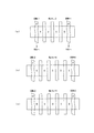
半導体集積回路の微細化プロセス技術において、例えば、半導体ウェハに形成される回路素子の1つであるMOSトランジスタを複数、共有部分(ドレイン領域及びソース領域)を介して連続して接続した構成のマルチMOS回路の形成プロセスがある。このマルチMOS回路において、Vthが場所によって異なる現象が発生するという問題がある。この現象は、マルチMOS回路における連続接続されたMOSトランジスタの両端のゲートの形状と、その内側のMOSトランジスタのゲートの形状とが異なることが原因で生じることが判明している。図19に、そのイメージを示す(マルチ数=4のマルチMOS回路)。図19を見ると、両端のゲートの形状が内側のゲートの形状と異なっている様子が解る。この問題に対して、マルチMOS回路の両端にダミーMOSを付加する設計手法(図19の下図)が採用されている。この設計手法を用いることで、内側のMOSのマッチングが取れ、上記問題を回避することができる(例えば、特許文献1参照。)。 In the miniaturization process technology of a semiconductor integrated circuit, for example, a multi-structure having a configuration in which a plurality of MOS transistors, which are one of circuit elements formed on a semiconductor wafer, are continuously connected via a shared portion (drain region and source region). There is a process for forming a MOS circuit. In this multi-MOS circuit, there is a problem that a phenomenon in which V th varies depending on the location. It has been found that this phenomenon occurs due to the difference between the gate shapes of both ends of the MOS transistors connected continuously in the multi-MOS circuit and the gate shapes of the MOS transistors inside the MOS transistors. FIG. 19 shows an image thereof (multi-MOS circuit with multi-number = 4). Referring to FIG. 19, it can be seen that the shape of the gates at both ends is different from the shape of the inner gate. In order to solve this problem, a design method (lower diagram in FIG. 19) is adopted in which dummy MOSs are added to both ends of the multi-MOS circuit. By using this design method, the inner MOS can be matched and the above problem can be avoided (see, for example, Patent Document 1).
特許文献1の半導体装置は、中央部の内部セル領域を取り囲むように配線チャネル領域を設け、さらにその周囲を外部との信号の入出力等を行う回路配置されたI/Oセル領域が取り囲む構成の半導体装置において、内部セル領域の内部に設けられた多数のMOSトランジスタと寸法および配置密度がほぼ同一なダミーMOSトランジスタを配線チャネル領域に形成し、内部セル領域における辺縁部のMOSトランジスタの配置密度環境が、中央部のMOSトランジスタ群と等価になるようにして、製造時における拡散層パターンやゲートパターンの寸法ばらつきを防止するものである。
The semiconductor device of
図19の下図は、長破線で囲まれる部分が本体部、すなわち本来のMOSトランジスタの部分を示し、短破線で囲まれる部分がダミーとして付加されたMOSトランジスタ、すなわちダミーMOS部を示す。図19中の大文字のS、Dはそれぞれソース、ドレインを示し、小文字dで示した部分はダミーMOSのゲートを示し、S、Dに挟まれた何も無い縦長の長方形が本体部のゲートを示す。
しかしながら、上記従来の設計手法を採用した場合に、半導体集積回路に係る回路図を設計するCADや、半導体集積回路のマスクパターンを設計するCADなどを用いて、ダミーMOSを本体のMOSに1つずつ手入力で付加しなければならない。更に、ダミーMOSを1つ付加する毎に、付加した後のマルチMOS回路に対して、その検証(LVS:Layout Versus Schematic)を行わなくてはならない。そのため、設計者は、非効率で確実性の無い作業を強いられているのが現状である。 However, when the above conventional design method is adopted, one dummy MOS is used as the main body MOS by using CAD for designing a circuit diagram related to a semiconductor integrated circuit, CAD for designing a mask pattern of a semiconductor integrated circuit, or the like. It must be added manually. Furthermore, every time one dummy MOS is added, the verification (LVS: Layout Versus Schematic) must be performed on the added multi-MOS circuit. Therefore, the current situation is that designers are forced to perform inefficient and uncertain work.
そこで、本発明は、このような従来の技術の有する未解決の課題に着目してなされたものであって、MOSトランジスタなどの回路素子を連続接続してなるマルチ素子回路を含む半導体集積回路に係る回路図を設計するのに好適な回路図設計装置、回路図設計プログラム及び回路図設計方法を提供することを目的としている。 Therefore, the present invention has been made paying attention to such an unsolved problem of the conventional technology, and is applied to a semiconductor integrated circuit including a multi-element circuit in which circuit elements such as MOS transistors are continuously connected. An object of the present invention is to provide a circuit diagram design apparatus, a circuit diagram design program, and a circuit diagram design method suitable for designing such a circuit diagram.
〔発明1〕 上記目的を達成するために、発明1の回路図設計装置は、表示装置の画面上に表示されるレイアウト領域に、半導体集積回路を構成する各種回路素子に対応する回路記号と配線パターンとをレイアウトすることで、前記半導体集積回路に係る回路図を設計することが可能な回路図設計装置であって、前記回路図の設計に係る前記回路記号を選択する回路記号選択手段と、前記回路記号選択手段で選択された前記回路記号のうち特定の回路記号に対して、該特定の回路記号の示す回路素子の連続形成数を示すパラメータと、該連続形成数の回路素子を連続して一繋がりに形成して成るマルチ素子回路の動作特性のバラツキを低減するための付加素子であるダミー素子の形成数を示すパラメータとを含むパラメータを設定するパラメータ設定手段と、前記パラメータ設定手段で前記特定の回路記号に対して前記パラメータが設定されたときに、該設定されたパラメータの内容が正しいか誤りかを判定するパラメータ判定手段と、前記パラメータ判定手段の判定結果が誤りであるという判定結果であったときに、前記特定の回路記号に対して設定されたパラメータを予め設定された修正方法に基づき正しい内容に修正するパラメータ修正手段と、前記レイアウト領域にレイアウトされた回路記号及び配線パターンの情報と、前記パラメータ設定手段で設定されたパラメータとに基づき、前記マルチ素子回路を構成する各回路素子を含む前記レイアウトされた各回路記号の示す回路素子の接続関係を示す接続関係情報を生成する接続関係情報生成手段と、前記接続関係情報に基づき前記回路記号及び前記配線パターンを含んで構成されるシンボル回路図を表示する回路図表示手段と、を備える。
[Invention 1] In order to achieve the above object, a circuit diagram design apparatus of
このような構成であれば、回路記号選択手段によって、例えば、選択画面に表示された回路記号のうちパラメータが設定可能な特定の回路記号、又はレイアウト領域にレイアウトされた回路記号のうちパラメータが設定可能な特定の回路記号が選択されると、パラメータ設定手段によって、選択された特定の回路記号に対して、その回路素子の連続形成数及びダミー素子の形成数を示すパラメータを含むマルチ素子回路を生成するためのパラメータを設定することが可能である。特定の回路記号に対してパラメータが設定されると、パラメータ判定手段によって、設定されたパラメータ値の設定内容が正しいか誤りかが判定され、判定結果が誤りであるという判定結果のときに、パラメータ修正手段によって、特定の回路記号に対して設定された誤った設定内容のパラメータが、予め設定された修正方法に基づき正しい設定内容に自動的に修正される。 In such a configuration, the circuit symbol selection means, for example, sets a specific circuit symbol in which a parameter can be set among circuit symbols displayed on the selection screen or a parameter among circuit symbols laid out in the layout area. When a possible specific circuit symbol is selected, a multi-element circuit including a parameter indicating the number of continuous formations of the circuit elements and the number of formations of dummy elements is selected by the parameter setting means for the selected specific circuit symbol. It is possible to set parameters for generation. When a parameter is set for a specific circuit symbol, the parameter determination means determines whether the set content of the set parameter value is correct or incorrect. When the determination result indicates that the determination result is incorrect, the parameter The parameter of the erroneous setting content set for the specific circuit symbol is automatically corrected by the correcting means to the correct setting content based on a preset correction method.
一方、選択された特定の回路記号に対して正しいパラメータが設定されると、接続関係情報生成手段によって、レイアウト領域にレイアウトされた回路記号及び配線パターンの情報と、特定の回路記号に設定されたパラメータとに基づき、マルチ素子回路を構成する各回路素子を含むレイアウトされた各回路記号の示す回路素子の接続関係を示す接続関係情報が生成される。 On the other hand, when the correct parameter is set for the selected specific circuit symbol, the connection relation information generating means sets the circuit symbol and wiring pattern information laid out in the layout area and the specific circuit symbol. Based on the parameters, connection relation information indicating the connection relation of the circuit elements indicated by the respective circuit symbols laid out including the circuit elements constituting the multi-element circuit is generated.
また、接続関係情報が生成されると、回路図表手段によって、該生成された接続関係情報に基づき、回路記号及び配線パターンを含んで構成されるシンボル回路図が表示される。
従って、半導体基板(半導体ウェーハ)に形成される、能動素子(例えば、ダイオード、トランジスタなど)や、受動素子(例えば、抵抗、キャパシタ、インダクタなど)などの回路素子を、同じ回路素子同士で複数を連続接続(例えば、各回路素子の一部を他と共有させてひと繋がりに形成)した構成のマルチ素子回路を含む半導体集積回路を設計(作成)するときに、例えば、手作業で同じ回路記号を1つずつ選択して形成することなく、選択した回路記号に対して連続形成数をパラメータ設定するだけで、該回路記号の回路素子を連続接続した構成のマルチ素子回路を生成することができる。
When the connection relation information is generated, the circuit diagram means displays a symbol circuit diagram including a circuit symbol and a wiring pattern based on the generated connection relation information.
Accordingly, a plurality of circuit elements such as active elements (for example, diodes, transistors, etc.) and passive elements (for example, resistors, capacitors, inductors, etc.) formed on a semiconductor substrate (semiconductor wafer) can be used. When designing (creating) a semiconductor integrated circuit including a multi-element circuit having a configuration in which continuous connection (for example, a part of each circuit element is shared and formed in a single connection), for example, the same circuit symbol is used manually. A multi-element circuit having a configuration in which the circuit elements of the circuit symbol are continuously connected can be generated simply by setting the number of consecutive formations for the selected circuit symbol without selecting and forming each one. .
更に、マルチ素子回路において、例えば、該マルチ素子回路を構成する回路素子の一部の形状の違いなどから生じるマルチ素子回路の動作特性のバラツキを低減するため付加素子であるダミー素子についても、選択した回路記号に対してダミー素子の形成数をパラメータ設定するだけで、手作業でダミー素子の回路記号を1つずつ選択して形成することなく、連続接続された回路素子にダミー素子が付加接続された構成のマルチ素子回路を生成することができる。 In addition, in a multi-element circuit, for example, a dummy element that is an additional element is also selected in order to reduce variation in operating characteristics of the multi-element circuit caused by a difference in the shape of a part of the circuit elements constituting the multi-element circuit. By simply setting parameters for the number of dummy elements formed for each circuit symbol, the dummy elements can be added to the continuously connected circuit elements without manually selecting and forming the dummy element circuit symbols one by one. A multi-element circuit having the above-described configuration can be generated.
これによって、選択した回路記号に対してパラメータを設定するといった簡単な作業で、任意のダミー素子を含むマルチ素子回路を含む回路の接続関係情報を生成することができるという効果が得られる。
また、回路素子のマルチ数やダミー素子の数をパラメータで管理するようにしたので、確実にダミー素子を付加することができ、レイアウト検証(LVS)を、より確実に行うことができるという効果が得られる。
As a result, it is possible to generate connection relation information of a circuit including a multi-element circuit including an arbitrary dummy element by a simple operation of setting a parameter for the selected circuit symbol.
In addition, since the number of circuit elements and the number of dummy elements are managed by parameters, dummy elements can be added reliably, and layout verification (LVS) can be more reliably performed. can get.
また、選択した回路記号に対してパラメータを設定するので、本来の回路素子の連続接続数の情報とこの回路素子に付加的に接続されるダミー素子の情報とが関連付けられるので、この情報を、半導体集積回路のマスクパターンの生成に利用することで、マスクパターンの生成においても、ダミー素子を1つ1つ手作業で付加するといった労力を軽減することができるという効果が得られる。 In addition, since the parameter is set for the selected circuit symbol, the information on the number of continuous connections of the original circuit elements and the information on the dummy elements additionally connected to the circuit elements are associated with each other. By using it for generating a mask pattern of a semiconductor integrated circuit, it is possible to reduce the labor of manually adding dummy elements one by one even when generating a mask pattern.
更に、パラメータ判定手段によって設定内容の正誤判定を行ない、設定内容に誤りがあったときは、パラメータ修正手段によって修正を行なうようにした。これによって、ユーザの設定内容に間違いがあったときや、例えばパラメータMultiの数値を意図的に変更してパラメータDDM及びSDMの値との間に不整合が生じたときなどに、パラメータ修正手段が自動で正しい設定内容に修正を行ってくれるので、手作業による修正を行うことなく、簡易且つ確実に正しいパラメータ設定内容のマルチ素子回路を生成することができるという効果が得られる。 Further, the correctness / incorrectness of the setting contents is determined by the parameter determining means, and when there is an error in the setting contents, the parameter correcting means corrects the setting contents. As a result, when there is an error in the setting contents of the user, for example, when there is a mismatch between the values of the parameters DDM and SDM by intentionally changing the value of the parameter Multi, the parameter correction means Since the correct setting contents are automatically corrected, it is possible to easily and surely generate a multi-element circuit having the correct parameter setting contents without performing manual correction.
ここで、上記回路記号は、例えば、JIS C 0301 、JIS C 0617、JIS C 9309、JIS B 8601などのJISに準拠した回路記号や、これらの回路記号を基準にして作成されたもの、また、マスクパターンの生成にも対応させる場合は、各回路素子に対応するマスクパターンのセル、ブロックなどが該当する。
また、上記半導体集積回路に係る回路図は、例えば、上記JISに準拠した回路記号や配線パターンで表された回路図であるシンボル回路図や、セル、ブロックなどの回路記号で表されたマスクパターンのレイアウト図であるパターンレイアウト図などが該当する。以下、発明7の回路図設計プログラム、発明8の回路図設計方法において同じである。
Here, the circuit symbol is, for example, a circuit symbol compliant with JIS, such as JIS C 0301, JIS C 0617, JIS C 9309, JIS B 8601, or the like, created based on these circuit symbols, When the mask pattern generation is also supported, the mask pattern cell, block, and the like corresponding to each circuit element are applicable.
The circuit diagram relating to the semiconductor integrated circuit is, for example, a symbol circuit diagram which is a circuit diagram represented by a circuit symbol or wiring pattern compliant with the JIS, or a mask pattern which is represented by a circuit symbol such as a cell or a block. This corresponds to a pattern layout diagram that is a layout diagram. The same applies to the circuit diagram design program of the seventh invention and the circuit diagram design method of the eighth invention.
また、上記回路記号選択手段は、例えば、表示装置の画面上に回路記号の一覧を表示し、その中から任意の回路シンボルを選択したり、レイアウト領域にレイアウトされたシンボル回路図を構成する回路シンボルを選択したりする構成などが該当する。また、選択処理は、例えば、入力デバイス(マウス、タブレット、キーボードなど)を用いた利用者の操作入力に応じて行われ、利用者の任意の回路記号を選択できるようになっている。また、回路記号の一覧表示は、例えば、回路素子の種類毎に一覧を表示(一覧できないときは、ページ分けして表示)する。以下、発明7の回路図設計プログラム、発明8の回路図設計方法において同じである。 The circuit symbol selection means displays a list of circuit symbols on a screen of a display device, for example, selects an arbitrary circuit symbol from the list, or configures a symbol circuit diagram laid out in a layout area A configuration for selecting a symbol is applicable. In addition, the selection process is performed in accordance with, for example, a user operation input using an input device (such as a mouse, a tablet, or a keyboard), and an arbitrary circuit symbol of the user can be selected. The list display of the circuit symbols is, for example, a list for each type of circuit element (when the list cannot be displayed, it is displayed by dividing into pages). The same applies to the circuit diagram design program of the seventh invention and the circuit diagram design method of the eighth invention.
また、上記マルチ素子回路は、例えば、半導体基板に形成されるMOSトランジスタなどの能動素子、抵抗、コンデンサなどの受動素子などの回路素子を、同じものを複数連続して形成することで構成されるものである。このとき、例えば、MOSトランジスタであれば、隣り合う素子同士でソース領域やドレイン領域を共有するように連続形成される。
更に、複数の回路素子を連続形成したときに、各回路素子の形状などの違いによって生じる動作特性のバラツキを低減するために、例えば、連続形成部の両端にダミー素子として同じ種類、特性の回路素子を付加する。以下、発明7の回路図設計プログラム、発明8の回路図設計方法において同じである。
The multi-element circuit is configured by, for example, continuously forming a plurality of circuit elements such as active elements such as MOS transistors formed on a semiconductor substrate and passive elements such as resistors and capacitors. Is. At this time, for example, in the case of a MOS transistor, they are continuously formed so that adjacent elements share a source region and a drain region.
Furthermore, in order to reduce variation in operating characteristics caused by differences in the shape of each circuit element when a plurality of circuit elements are continuously formed, for example, circuits of the same type and characteristics as dummy elements at both ends of the continuous formation portion Add elements. The same applies to the circuit diagram design program of the seventh invention and the circuit diagram design method of the eighth invention.
また、上記接続関係情報生成手段は、例えば、レイアウト領域にレイアウトされた回路記号及び配線パターンから構成されるシンボル回路図の各回路記号の示す回路素子の識別情報と、各回路素子、各ダミー素子の各端子の接続情報とを含む、接続関係情報(例えば、SPICE(Simulation Program with Integrated Circuit Emphasis)のネットリストなど)を生成する。更に、特定の回路記号に対してパラメータが設定されたときは、その設定値に基づき、連続形成する各回路素子の識別情報と、ダミー素子などの各付加素子の識別情報と、各回路素子、各付加素子の各端子の接続情報とを含む、マルチ素子回路の接続関係情報を生成する。以下、発明7の回路図設計プログラム、発明8の回路図設計方法において同じである。 In addition, the connection relation information generating means includes, for example, circuit element identification information indicated by each circuit symbol of a symbol circuit diagram composed of circuit symbols and wiring patterns laid out in a layout area, each circuit element, and each dummy element. Connection relation information (for example, a net list of SPICE (Simulation Program with Integrated Circuit Emphasis) or the like) is generated. Further, when a parameter is set for a specific circuit symbol, based on the set value, identification information of each circuit element to be continuously formed, identification information of each additional element such as a dummy element, each circuit element, Multi-element circuit connection relation information including connection information of each terminal of each additional element is generated. The same applies to the circuit diagram design program of the seventh invention and the circuit diagram design method of the eighth invention.
〔発明2〕 更に、発明2の回路図設計装置は、発明1に記載の回路図設計装置において、前記パラメータ設定手段は、前記回路記号選択手段でMOS(metal-oxide-semiconductor)トランジスタの回路記号が選択されたときに、該MOSトランジスタの回路記号に対して、該MOSトランジスタの連続形成数を示すパラメータMultiと、該M個のMOSトランジスタを、ドレインとソースの領域を行方向となる一方向に交互に反復させながら一繋がりに形成したときの前記行方向の端部のドレイン領域に付加されるダミーMOSトランジスタの形成数を示すパラメータDDMと、前記行方向の端部のソース領域に付加されるダミーMOSトランジスタの形成数を示すパラメータSDMとを含むパラメータを設定することが可能であり、前記パラメータ判定手段は、前記パラメータMultiが偶数値に設定され且つ前記行方向の両端部が共にソース領域又はドレイン領域となるときに、前記パラメータDDM及び前記パラメータSDMにそれぞれ0以外の数値が設定される第1の設定内容と、前記パラメータMultiが偶数値に設定され且つ前記行方向の両端部が共にソース領域となるときに、前記パラメータDDMに0が設定され且つ前記パラメータSDMに1以下の数値又は3以上の奇数値が設定される第2の設定内容と、前記パラメータMultiが偶数値に設定され且つ前記行方向の両端部がドレイン領域となるときに、前記パラメータDDMに1以下の数値又は3以上の奇数値が設定され且つ前記パラメータSDMに0が設定される第3の設定内容とのうちいずれか1つの設定内容で、前記MOSトランジスタの回路記号に対してパラメータが設定されたときに、該パラメータの設定内容が誤りであると判定し、前記パラメータ修正手段は、前記第1の設定内容による誤り判定に対して、前記行方向の両端部が共にソース領域のときは、前記パラメータDDMの設定値が0で且つ前記パラメータSDMの設定値が所定の偶数値となるように設定値を修正し、前記行方向の両端部がドレイン領域のときは、前記パラメータDDMの設定値が所定の偶数値で且つ前記パラメータSDMの設定値が0となるように設定値を修正し、前記第2の設定内容による誤り判定に対して、前記パラメータSDMの設定値を所定の偶数値に修正し、前記第3の設定内容による誤り判定に対して、前記パラメータDDMの設定値を所定の偶数値に修正する。
[Invention 2] Further, the circuit diagram design apparatus according to
このような構成であれば、回路記号選択手段で選択されたMOSトランジスタの回路記号に対して、上記第1〜第3のいずれか1つの設定内容でパラメータが設定されると、パラメータ判定手段において、設定内容が誤りであると判定される。誤り判定がされると、パラメータ修正手段において、第1〜第3の設定内容のうち設定された内容に応じた修正方法で修正が行われる。具体的に、パラメータ修正手段は、第1の設定内容で設定が行われた場合に、パラメータDDM及びSDMの双方に0以外の数値が設定されているときは、両端がドレイン領域であれば、パラメータDDMの設定値が所定の偶数で且つパラメータSDMの設定値が0となるように設定値を修正する。一方、両端がソース領域であれば、パラメータSDMの設定値が所定の偶数で且つパラメータDDMの設定値が0となるように設定値を修正する。 With such a configuration, when a parameter is set according to any one of the first to third settings for the circuit symbol of the MOS transistor selected by the circuit symbol selection means, the parameter determination means , It is determined that the setting content is incorrect. When an error determination is made, the parameter correction means performs correction by a correction method according to the set contents among the first to third setting contents. Specifically, the parameter correction means is configured so that when both the parameters DDM and SDM are set to numerical values other than 0 when both are set in the first setting content, both ends are drain regions. The setting value is corrected so that the setting value of the parameter DDM is a predetermined even number and the setting value of the parameter SDM becomes zero. On the other hand, if both ends are source regions, the setting value is corrected so that the setting value of the parameter SDM is a predetermined even number and the setting value of the parameter DDM is zero.
また、第2の設定内容で設定が行われた場合に、パラメータSDMの設定値を所定の偶数値に修正し、第3の設定内容で設定が行われた場合に、パラメータDDMの設定値を所定の偶数値に修正する。
従って、マルチ素子回路を作成できるMOSトランジスタの回路記号に対して、誤ったパラメータを設定したときや、意図的にパラメータMultiの設定値を変更してパラメータDDM及びSDMの設定値との間に不整合が生じたときなどに、適切な内容のパラメータに自動的に修正することができる。
これにより、MOSトランジスタによって構成されるマルチ素子回路を、適切な回路構成で、より確実に作成することができるという効果が得られる。
In addition, when the setting is performed with the second setting content, the setting value of the parameter SDM is corrected to a predetermined even value, and when the setting is performed with the third setting content, the setting value of the parameter DDM is changed. Correct to a given even value.
Therefore, when an incorrect parameter is set for the circuit symbol of the MOS transistor capable of creating a multi-element circuit, or when the setting value of the parameter Multi is changed intentionally, it is not between the setting values of the parameters DDM and SDM. When matching occurs, the parameter can be automatically corrected to an appropriate content.
As a result, an effect is obtained that a multi-element circuit constituted by MOS transistors can be more reliably created with an appropriate circuit configuration.
〔発明3〕 更に、発明3の回路図設計装置は、発明1又は2に記載の回路図設計装置において、前記パラメータ設定手段は、前記回路記号選択手段でMOS(metal-oxide-semiconductor)トランジスタの回路記号が選択されたときに、前記パラメータMultiと、前記パラメータDDMと、前記パラメータSDMと、前記マルチ素子回路の前記行方向と直交する方向である列方向の形成数を示すパラメータROWとを含むパラメータを設定することが可能であり、前記接続関係情報生成手段は、前記パラメータROWに2以上の数値が設定されたときに、前記パラメータMultiの設定値を前記パラメータROWの設定値で割った数値をMOSトランジスタの前記連続形成数としたマルチ素子回路を、前記パラメータROWの数だけ前記列方向に連続して接続した構成のマルチ素子回路列の各回路素子の接続関係を示す接続関係情報を生成し、前記パラメータMultiの設定値(2以上の整数)を前記パラメータROWの設定値(Mの設定値>ROWの設定値≧1の整数)で除算した除算結果の数値をカラムパラメータの数値とし、前記パラメータMultiの設定値が前記パラメータROWの設定値で割り切れるときに、前記パラメータ判定手段は、前記パラメータROWが2以上の整数値に設定され且つ前記カラムパラメータの数値が奇数値となり、前記パラメータDDM及び前記パラメータSDMの少なくとも一方に前記パラメータROWの設定値をN倍(Nは1以上の整数)した数値とは異なる数値が設定される第4の設定内容と、前記パラメータROWが2以上の整数値に設定され且つ前記カラムパラメータの数値が偶数値となり、前記パラメータDDM及び前記パラメータSDMの少なくとも一方に前記パラメータROWの設定値をM倍(Mは2以上の偶数)にした数値とは異なる数値が設定される第5の設定内容とのうちいずれか1つの設定内容で、前記MOSトランジスタの回路記号に対してパラメータが設定されたときに、該パラメータの設定内容が誤りであると判定し、前記パラメータ修正手段は、前記第4の設定内容による誤り判定に対して、前記パラメータDDMの設定値及び前記パラメータSDMの設定値のうち前記パラメータROWの設定値をN倍した数値とは異なる数値が設定されているものを、前記パラメータROWの設定値となるように修正し、前記第5の設定内容による誤り判定に対して、前記行方向の両端部が共にソース領域のときは、前記パラメータDDMの設定値が0以外の数値のときは該設定値を0に且つ前記パラメータSDMの設定値を前記パラメータROWの設定値をM倍にした数値に修正し、前記行方向の両端部がドレイン領域のときは、前記パラメータDDMの設定値を前記パラメータROWの設定値をM倍にした数値に且つ前記パラメータSDMの設定値が0以外の数値のときは該設定値を0に修正する。
[Invention 3] Further, the circuit diagram design apparatus according to the
このような構成であれば、パラメータROWの数値を2以上に設定することで、複数のマルチ素子回路が、設定値の数だけ列方向に連続して接続された構成のマルチ素子回路列を生成することができる。更に、パラメータMultiの設定値(2以上の整数)をパラメータROWの設定値(Mの設定値>ROWの設定値≧1の整数)で除算して割り切れるときに、上記第4〜第5の設定内容で、MOSトランジスタの回路記号に対して、パラメータが設定されると、パラメータ判定手段において、設定内容が誤りであると判定される。 In such a configuration, by setting the numerical value of the parameter ROW to 2 or more, a multi-element circuit array having a configuration in which a plurality of multi-element circuits are continuously connected in the column direction by the number of set values is generated. can do. Further, when the setting value of the parameter Multi (an integer of 2 or more) is divided by the setting value of the parameter ROW (the setting value of M> the setting value of ROW ≧ an integer of 1), the above fourth to fifth settings When the parameter is set for the circuit symbol of the MOS transistor, the parameter determination means determines that the setting content is incorrect.
誤り判定がされると、パラメータ修正手段において、第4〜第5の設定内容のうち設定された内容に応じた修正方法で修正が行われる。
具体的に、パラメータ修正手段は、第4の設定内容で設定が行われた場合に、パラメータDDMの設定値及びパラメータSDMの設定値のうちパラメータROWの設定値とは異なる数値が設定されているものを、パラメータROWの設定値となるように修正する。
When an error determination is made, the parameter correction means performs correction by a correction method according to the set contents among the fourth to fifth set contents.
Specifically, the parameter correction means sets a value different from the setting value of the parameter ROW among the setting value of the parameter DDM and the setting value of the parameter SDM when the setting is performed with the fourth setting content. Is corrected so as to be the set value of the parameter ROW.
また、第5の設定内容で設定が行われた場合に、行方向の両端部が共にソース領域のときは、パラメータDDMの設定値が0以外の数値のときは該設定値を0に且つパラメータSDMの設定値をパラメータROWの設定値をM倍にした数値に修正し、行方向の両端部がドレイン領域のときは、パラメータDDMの設定値をパラメータROWの設定値をM倍にした数値に且つパラメータSDMの設定値が0以外の数値のときは該設定値を0に修正する。 In addition, when setting is performed with the fifth setting content, when both end portions in the row direction are source regions, when the setting value of the parameter DDM is a value other than 0, the setting value is set to 0 and the parameter The SDM setting value is corrected to a value obtained by multiplying the setting value of the parameter ROW by M times. When both ends in the row direction are drain regions, the setting value of the parameter DDM is changed to a value obtained by multiplying the setting value of the parameter ROW by M times. If the setting value of the parameter SDM is a value other than 0, the setting value is corrected to 0.
従って、マルチ素子回路列を作成できるMOSトランジスタの回路記号に対して、誤ったパラメータを設定したときや、意図的にパラメータMultiやROWの設定値を変更してパラメータDDM及びSDMの設定値との間に不整合が生じたときなどに、適切な内容のパラメータに自動的に修正することができる。
これにより、MOSトランジスタによって構成されるマルチ素子回路列を、適切な回路構成で、より確実に作成することができるという効果が得られる。
ここで、上記マルチ素子回路列は、各列のマルチ素子回路を構成するMOSトランジスタのゲート領域、ドレイン領域、ソース領域を列方向に共有して構成されるものなどが該当する。
Therefore, when an incorrect parameter is set for a circuit symbol of a MOS transistor that can create a multi-element circuit row, or when the setting values of the parameters Multi and ROW are intentionally changed, the setting values of the parameters DDM and SDM are changed. When inconsistency occurs, the parameter can be automatically corrected to an appropriate content.
As a result, an effect is obtained that a multi-element circuit array composed of MOS transistors can be more reliably created with an appropriate circuit configuration.
Here, the multi-element circuit column corresponds to a configuration in which the gate region, the drain region, and the source region of the MOS transistors constituting the multi-element circuit of each column are shared in the column direction.
〔発明4〕 更に、発明4の回路図設計装置は、発明1乃至3のいずれか1に記載の回路図設計装置において、前記回路図表示手段は、前記接続関係情報生成手段で生成された接続関係情報に基づき、前記半導体集積回路のマスクパターンのレイアウトを示すパターンレイアウト図を表示し、前記回路図表示手段で表示されたパターンレイアウト図を編集するレイアウト編集手段を備え、前記パラメータ修正手段は、前記レイアウト編集手段で前記パターンレイアウト図の編集が行われたときに、その編集結果に基づき前記特定の回路記号に設定されたパラメータを修正し、前記接続関係情報生成手段は、前記レイアウト編集手段で前記パターンレイアウト図の編集が行われたときに、その編集結果と前記パラメータ修正手段の修正結果とに基づき前記接続関係情報を修正する。
[Invention 4] Further, the circuit diagram design apparatus according to the
このような構成であれば、回路図表示手段によって、JISに準拠する回路記号をレイアウト領域にレイアウトしたり、特定の回路記号に対してパラメータを設定したりするなどして構成されたシンボル回路図に対して生成された接続関係情報に基づき、パターンレイアウト図を表示するための表示情報を生成し、該生成した表示情報に基づきマルチ素子回路のマスクパターンを含むパターンレイアウト図を表示することが可能である。 With such a configuration, a symbol circuit diagram configured by laying out circuit symbols conforming to JIS in the layout area or setting parameters for specific circuit symbols by means of circuit diagram display means. Display information for displaying a pattern layout diagram can be generated based on the connection relation information generated for the pattern, and a pattern layout diagram including a mask pattern of a multi-element circuit can be displayed based on the generated display information. It is.
更に、レイアウト編集手段によって、表示されたレイアウト図の編集を行うことが可能であり、編集が行われると、パラメータ修正手段によって、レイアウト編集手段の編集結果に基づき、特定の回路記号に対して設定されたパラメータが修正され、接続関係情報生成手段によって、編集手段の編集結果とパラメータ修正手段の修正結果に基づき接続関係情報が修正される。 Furthermore, it is possible to edit the displayed layout diagram by the layout editing means. When the editing is performed, the parameter correction means sets the specific circuit symbol based on the editing result of the layout editing means. The connection parameter information is corrected, and the connection relationship information generation unit corrects the connection relationship information based on the editing result of the editing unit and the correction result of the parameter correction unit.
従って、パターンレイアウト図に対して編集が行われたときに、その編集によって、マルチ素子回路の連続形成数などが変更されて、ダミー素子の数などに変更の必要性が生じたときに、パラメータ修正手段によってパラメータを自動的に適切な設定値に修正し、且つ、接続関係情報生成手段によって、前記修正結果と前記編集結果とに基づき、接続関係情報を自動的に適切な内容に修正することができる。 Therefore, when the pattern layout diagram is edited, the parameter changes when the number of continuous formations of multi-element circuits is changed by the editing and the number of dummy elements needs to be changed. The parameter is automatically corrected to an appropriate set value by the correcting means, and the connection relation information is automatically corrected to an appropriate content based on the correction result and the editing result by the connection relation information generating means. Can do.
これによって、パターンレイアウト図を編集して、マルチ素子回路の構成が変更されたときでも、その回路記号に対して設定されたパラメータを適切な値に自動で修正し、且つこの修正結果の反映された接続関係情報を自動で生成することができるので、手作業による修正と比較して、より確実に適切な構成のマルチ素子回路を含む回路及びマスクパターンを設計することができ、且つ設計した回路に対する検証(LVS)をより確実に行うことができるという効果が得られる。 As a result, even when the pattern layout diagram is edited and the configuration of the multi-element circuit is changed, the parameters set for the circuit symbol are automatically corrected to appropriate values, and the correction results are reflected. Since the connection relation information can be automatically generated, it is possible to design a circuit and a mask pattern including a multi-element circuit having an appropriate configuration more reliably than the manual correction, and the designed circuit. The effect that verification (LVS) can be performed more reliably is obtained.
〔発明5〕 更に、発明5の回路図設計装置は、発明3に記載の回路図設計装置において、前記回路図表示手段は、前記接続関係情報生成手段で生成された接続関係情報に基づき、前記半導体集積回路のマスクパターンのレイアウトを示すパターンレイアウト図を表示し、前記回路図表示手段で表示されたパターンレイアウト図を編集するレイアウト編集手段を備え、前記パラメータ修正手段は、前記レイアウト編集手段で前記パターンレイアウト図の編集が行われたときに、その編集結果に基づき前記特定の回路記号に設定されたパラメータを修正し、前記接続関係情報生成手段は、前記レイアウト編集手段で前記パターンレイアウト図の編集が行われたときに、その編集結果と前記パラメータ修正手段の修正結果とに基づき前記接続関係情報を修正し、前記レイアウト編集手段によって、前記MOSトランジスタを含んで構成されるマルチ素子回路の列方向の形成数が変更されたときに、前記パラメータ修正手段は、前記パラメータMultiの設定値を該設定値を前記形成数倍にした数値に修正すると共に前記パラメータROWの設定値を前記変更した形成数に修正し、前記カラムパラメータの数値が奇数値のときは、前記パラメータDDMの設定値及び前記パラメータSDMの設定値を、それぞれ修正後の前記パラメータROWの設定値に修正し、前記カラムパラメータの数値が偶数値のときに、前記行方向の両端部が共にソース領域のときは、前記パラメータDDMの設定値が0以外の数値のときは該設定値を0に且つ前記パラメータSDMの設定値を前記修正後のパラメータROWの設定値をM倍にした数値に修正し、前記行方向の両端部がドレイン領域のときは、前記パラメータDDMの設定値を前記修正後のパラメータROWの設定値をM倍にした数値に且つ前記パラメータSDMの設定値が0以外の数値のときは該設定値を0に修正する。
[Invention 5] Further, the circuit diagram design apparatus according to Invention 5 is the circuit diagram design apparatus according to
このような構成であれば、回路図表示手段によって、JISに準拠する回路記号をレイアウト領域にレイアウトしたり、特定の回路記号に対してパラメータを設定したりするなどして構成された回路図に対して生成された接続関係情報に基づき、パターンレイアウト図を表示するための表示情報を生成し、該生成した表示情報に基づきマルチ素子回路のマスクパターンを含むパターンレイアウト図を表示することが可能である。 In such a configuration, the circuit diagram display means lays out a circuit symbol conforming to JIS in the layout area or sets a parameter for a specific circuit symbol. It is possible to generate display information for displaying the pattern layout diagram based on the connection relation information generated for the pattern layout diagram and display the pattern layout diagram including the mask pattern of the multi-element circuit based on the generated display information. is there.
更に、レイアウト編集手段によって、表示されたレイアウト図の編集を行うことが可能であり、編集が行われると、パラメータ修正手段によって、レイアウト編集手段の編集結果に基づき、特定の回路記号に対して設定されたパラメータが修正され、接続関係情報生成手段によって、編集手段の編集結果とパラメータ修正手段の修正結果に基づき接続関係情報が修正される。 Furthermore, it is possible to edit the displayed layout diagram by the layout editing means. When the editing is performed, the parameter correction means sets the specific circuit symbol based on the editing result of the layout editing means. The connection parameter information is corrected, and the connection relationship information generation unit corrects the connection relationship information based on the editing result of the editing unit and the correction result of the parameter correction unit.
なお更に、パラメータ修正手段は、レイアウト編集手段によって、前記MOSトランジスタを含んで構成されるマルチ素子回路の列方向の形成数が変更されたときに、パラメータMultiの設定値を前記列方向の形成数倍に修正すると共にパラメータROWの設定値を変更した形成数となるように修正する。更に、パラメータ修正手段は、カラムパラメータの数値が奇数値のときは、パラメータDDMの設定値及びパラメータSDMの設定値を、それぞれ修正後のパラメータROWの設定値に修正する。 Still further, the parameter correction means changes the setting value of the parameter Multi to the number of formations in the column direction when the number of formations in the column direction of the multi-element circuit including the MOS transistor is changed by the layout editing means. The number of formations is corrected so that the number of formations is changed by changing the setting value of the parameter ROW. Further, the parameter correcting means corrects the setting value of the parameter DDM and the setting value of the parameter SDM to the setting value of the parameter ROW after correction when the numerical value of the column parameter is an odd value.
一方、カラムパラメータの数値が偶数値のときに、行方向の両端部が共にソース領域となるときは、パラメータDDMの設定値が0以外の数値のときは該設定値を0に且つパラメータSDMの設定値を修正後のパラメータROWの設定値をM倍にした数値に修正し、行方向の両端部がドレイン領域となるときは、パラメータDDMの設定値を修正後のパラメータROWの設定値をM倍にした数値に且つパラメータSDMの設定値が0以外の数値のときは該設定値を0に修正する。 On the other hand, when the column parameter value is an even value and both end portions in the row direction are source regions, the set value of the parameter DDM is 0 and the set value of the parameter SDM is set to 0 when the set value of the parameter DDM is a value other than 0. When the setting value is corrected to a value obtained by multiplying the setting value of the parameter ROW after the correction by M times, and both ends in the row direction are drain regions, the setting value of the parameter DDM is changed to the setting value of the parameter ROW after correction. When the value is doubled and the setting value of the parameter SDM is a value other than 0, the setting value is corrected to 0.
従って、パターンレイアウト図に対して編集が行われたときに、その編集によって、MOSトランジスタを含んで構成されるマルチ素子回路の列方向の形成数が変更されて、パラメータDDM及びパラメータSDMなどに変更の必要性が生じたときに、パラメータ修正手段によって、パラメータROWの変更内容に応じてパラメータDDM及びパラメータSDMの設定値を適切な設定内容に自動で修正することができる。 Therefore, when the pattern layout diagram is edited, the number of formations in the column direction of the multi-element circuit including the MOS transistor is changed by the editing, so that the parameter DDM and the parameter SDM are changed. Therefore, the parameter correction means can automatically correct the setting values of the parameter DDM and the parameter SDM to the appropriate setting contents according to the change contents of the parameter ROW.
これによって、パターンレイアウト図を編集して、MOSトランジスタのマルチ素子回路列の構成が変更されたときでも、その回路記号に対して設定されたパラメータDDM及びパラメータSDMを適切な値に自動で修正し、且つこの修正結果の反映された接続関係情報を自動で生成することができるので、手作業による修正と比較して、より確実に適切な構成のマルチ素子回路を含む回路及びマスクパターンを設計することができ、且つ設計した回路に対する検証(LVS)をより確実に行うことができるという効果が得られる。 Thus, even when the configuration of the multi-element circuit array of MOS transistors is changed by editing the pattern layout diagram, the parameters DDM and SDM set for the circuit symbols are automatically corrected to appropriate values. In addition, since the connection relation information reflecting the correction result can be automatically generated, the circuit and the mask pattern including the multi-element circuit having an appropriate configuration can be more reliably designed as compared with the manual correction. And the verification (LVS) for the designed circuit can be performed more reliably.
〔発明6〕 更に、発明6の回路図設計装置は、発明4又は5に記載の回路図設計装置において、前記レイアウト編集手段は、複数の前記マルチ素子回路を、これらを構成する回路素子の回路パターンの一部を共有させて合成する第1の合成処理部と、複数の前記マルチ素子回路を、これらを構成する回路素子の回路パターンを所定の組み合わせで合体させて合成する第2の合成処理部とを有する。
[Invention 6] Further, the circuit diagram design apparatus according to the
このような構成であれば、第1の合成処理部による合成や、第2の合成処理部による合成が行われて、マルチ素子回路の構成が変更されたときでも、その回路記号に対して設定されたパラメータを適切な値に自動で修正し、且つこの修正結果の反映された接続関係情報を自動で生成することができるので、手作業による修正と比較して、より確実に適切な構成のマルチ素子回路を含む回路及びマスクパターンを設計することができ、且つ設計した回路に対する検証(LVS)をより確実に行うことができるという効果が得られる。 In such a configuration, even when the synthesis by the first synthesis processing unit or the synthesis by the second synthesis processing unit is performed and the configuration of the multi-element circuit is changed, the circuit symbol is set. Since it is possible to automatically correct the specified parameter to an appropriate value and automatically generate the connection relation information reflecting the correction result, it is possible to more reliably make the appropriate configuration as compared with the manual correction. It is possible to design a circuit including a multi-element circuit and a mask pattern, and to perform verification (LVS) on the designed circuit more reliably.
〔発明7〕 一方、上記目的を達成するために、発明7の回路図設計プログラムは、表示装置の画面上に表示されるレイアウト領域に、半導体集積回路を構成する各種回路素子に対応する回路記号と配線パターンとをレイアウトして、前記半導体集積回路に係る回路図を設計するために、コンピュータを、前記回路図の設計に係る前記回路記号を選択する回路記号選択手段、前記回路記号選択手段で選択された前記回路記号のうち特定の回路記号に対して、該特定の回路記号の示す回路素子の連続形成数を示すパラメータと、該連続形成数の回路素子を連続して一繋がりに形成して成るマルチ素子回路の動作特性のバラツキを低減するための付加素子であるダミー素子の形成数を示すパラメータとを含むパラメータを設定するパラメータ設定手段、前記パラメータ設定手段で前記特定の回路記号に対して前記パラメータが設定されたときに、該設定されたパラメータの内容が正しいか誤りかを判定するパラメータ判定手段、前記パラメータ判定手段の判定結果が誤りであるという判定結果であったときに、前記特定の回路記号に対して設定されたパラメータを予め設定された修正方法に基づき正しい内容に修正するパラメータ修正手段、前記レイアウト領域にレイアウトされた回路記号及び配線パターンの情報と、前記パラメータ設定手段で設定されたパラメータとに基づき、前記マルチ素子回路を構成する各回路素子を含む前記レイアウトされた各回路記号の示す回路素子の接続関係を示す接続関係情報を生成する接続関係情報生成手段、及び前記接続関係情報に基づき前記回路記号及び前記配線パターンを含んで構成されるシンボル回路図を表示する回路図表示手段として機能させる。
このような構成であれば、コンピュータによってプログラムが読み取られ、読み取られたプログラムに従ってコンピュータが処理を実行すると、上記発明1に記載の回路図設計装置と同等の作用および効果が得られる。
[Invention 7] On the other hand, in order to achieve the above object, a circuit diagram design program according to Invention 7 includes circuit symbols corresponding to various circuit elements constituting a semiconductor integrated circuit in a layout area displayed on a screen of a display device. In order to design a circuit diagram related to the semiconductor integrated circuit by laying out a wiring pattern and a circuit pattern, a computer uses a circuit symbol selecting means for selecting the circuit symbol related to the design of the circuit diagram, and the circuit symbol selecting means. For a specific circuit symbol among the selected circuit symbols, a parameter indicating the continuous formation number of the circuit elements indicated by the specific circuit symbol and the continuous formation circuit elements are formed in a continuous manner. Parameter setting means for setting a parameter including a parameter indicating the number of dummy elements that are additional elements for reducing variation in operating characteristics of the multi-element circuit A parameter determination unit that determines whether the content of the set parameter is correct or incorrect when the parameter is set for the specific circuit symbol by the parameter setting unit; a determination result of the parameter determination unit Parameter correction means for correcting a parameter set for the specific circuit symbol to a correct content based on a preset correction method, when the result is a determination result that the error is incorrect, laid out in the layout area Based on the circuit symbol and wiring pattern information and the parameters set by the parameter setting means, the connection relationship of the circuit elements indicated by the laid out circuit symbols including the circuit elements constituting the multi-element circuit is shown. Connection relation information generating means for generating connection relation information, and the circuit description based on the connection relation information. And to function as a circuit diagram display means for displaying the constructed symbol circuit diagram including the wiring pattern.
With such a configuration, when the program is read by the computer and the computer executes processing according to the read program, the same operation and effect as those of the circuit diagram design apparatus according to the first aspect of the invention can be obtained.
〔発明8〕 また、上記目的を達成するために、発明8の回路図設計方法は、回路記号選択手段、パラメータ設定手段、パラメータ判定手段、パラメータ修正手段、接続関係情報生成手段及び回路図表示手段を備えた回路図設計装置を利用して、表示装置の画面上に表示されるレイアウト領域に、半導体集積回路を構成する各種回路素子に対応する回路記号と配線パターンとをレイアウトして、前記半導体集積回路に係る回路図を設計する回路図設計方法であって、前記回路記号選択手段に、前記回路図の設計に係る前記回路記号を選択させる回路記号選択ステップと、前記パラメータ設定手段に、前記回路記号選択ステップで選択された前記回路記号のうち特定の回路記号に対して、該特定の回路記号の示す回路素子の連続形成数を示すパラメータと、該連続形成数の回路素子を連続して一繋がりに形成して成るマルチ素子回路の動作特性のバラツキを低減するための付加素子であるダミー素子の形成数を示すパラメータとを含むパラメータを設定させるパラメータ設定ステップと、前記パラメータ判定手段に、前記パラメータ設定ステップで前記特定の回路記号に対して前記パラメータが設定されたときに、該設定されたパラメータの内容が正しいか誤りかを判定させるパラメータ判定ステップと、前記パラメータ修正手段に、前記パラメータ判定ステップの判定結果が誤りであるという判定結果であったときに、前記特定の回路記号に対して設定されたパラメータを予め設定された修正方法に基づき正しい内容に修正するパラメータ修正ステップと、前記接続関係情報生成手段に、前記レイアウト領域にレイアウトされた回路記号及び配線パターンの情報と、前記パラメータ設定ステップで設定されたパラメータとに基づき、前記マルチ素子回路を構成する各回路素子を含む前記レイアウトされた各回路記号の示す回路素子の接続関係を示す接続関係情報を生成させる接続関係情報生成ステップと、前記回路図表示手段に、前記接続関係情報に基づき前記回路記号及び前記配線パターンを含んで構成されるシンボル回路図を表示させる回路図表示ステップとを含む。
このような構成であれば、上記発明1に記載の回路図設計装置と同等の作用及び効果が得られる。
[Invention 8] In order to achieve the above object, a circuit diagram design method of Invention 8 includes circuit symbol selection means, parameter setting means, parameter determination means, parameter correction means, connection relation information generation means, and circuit diagram display means. Laying out circuit symbols and wiring patterns corresponding to various circuit elements constituting a semiconductor integrated circuit in a layout area displayed on a screen of a display device by using a circuit diagram design apparatus comprising: A circuit diagram design method for designing a circuit diagram related to an integrated circuit, wherein the circuit symbol selection unit causes the circuit symbol selection unit to select the circuit symbol related to the design of the circuit diagram, and the parameter setting unit includes the For a specific circuit symbol among the circuit symbols selected in the circuit symbol selection step, a parameter indicating the number of consecutive circuit elements indicated by the specific circuit symbol. A parameter including a meter and a parameter indicating the number of dummy elements that are additional elements for reducing variation in operating characteristics of a multi-element circuit formed by continuously connecting the circuit elements of the continuous formation number. A parameter setting step for setting the parameter, and the parameter determination means determines whether the content of the set parameter is correct or incorrect when the parameter is set for the specific circuit symbol in the parameter setting step. A parameter determination step, and the parameter correction means, when the determination result of the parameter determination step is an error, the parameter set for the specific circuit symbol is corrected in advance A parameter correcting step for correcting the correct content based on the method, and the connection relation information generating means; The circuit symbols and circuit patterns laid out in the layout area and the parameters set in the parameter setting step are used to determine the layout of each circuit symbol including each circuit element constituting the multi-element circuit. A connection relationship information generating step for generating connection relationship information indicating the connection relationship of the circuit elements shown, and a symbol circuit diagram including the circuit symbol and the wiring pattern on the circuit diagram display means based on the connection relationship information. And a circuit diagram display step for displaying.
With such a configuration, operations and effects equivalent to those of the circuit diagram design apparatus according to the first aspect of the invention can be obtained.
以下、本発明の実施の形態を図面に基づき説明する。図1〜図18は、本発明に係る回路図設計装置、回路図設計プログラム及び回路図設計方法の実施の形態を示す図である。
まず、本発明に係る回路図設計装置の機能構成を図1に基づき説明する。図1は、本発明に係る回路図設計装置100の機能構成を示すブロック図である。
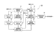
回路図設計装置100は、図1に示すように、回路記号情報記憶部10と、回路記号選択部12と、回路パターン編集部14と、回路表示情報生成部16と、回路図表示制御部18とを含んで構成される。
Hereinafter, embodiments of the present invention will be described with reference to the drawings. 1 to 18 are diagrams showing embodiments of a circuit diagram design apparatus, a circuit diagram design program, and a circuit diagram design method according to the present invention.
First, the functional configuration of the circuit diagram design apparatus according to the present invention will be described with reference to FIG. FIG. 1 is a block diagram showing a functional configuration of a circuit
As shown in FIG. 1, the circuit
回路記号情報記憶部10は、記憶装置(後述)の所定の記憶領域に構成されており、回路図を生成するための各種回路素子に対応した複数種類の回路記号の情報が記憶される。
具体的に、回路記号としては、シンボル回路図を生成するためのJISに準拠する回路記号(以下、回路シンボルと称す)や、マスクパターンを生成するためのセルやブロックなどの回路記号(以下、マスクシンボルと称す)などが記憶される。
The circuit symbol
Specifically, as a circuit symbol, a circuit symbol conforming to JIS for generating a symbol circuit diagram (hereinafter referred to as a circuit symbol), a circuit symbol such as a cell or block for generating a mask pattern (hereinafter referred to as a circuit symbol) Etc.) are stored.
回路記号選択部12は、マウス、キーボード、タブレットなどの入力装置を介した利用者からの操作入力に応じて、回路素子の情報選択画面や、回路記号の選択画面を表示装置の表示画面上に画像表示すると共に、画像表示された複数種類の回路記号の中から操作入力に応じた回路記号を選択する機能を有している。更に、操作入力に応じて、既にレイアウトされた回路記号や配線パターンなどの回路の任意の構成要素を選択する機能も有している。
The circuit
回路パターン編集部14は、入力装置を介した利用者からの操作入力に応じて、シンボル回路図の編集モード(以下、編集モード1と称す)において、回路記号選択部12で選択された回路シンボルや配線パターンを表示画面上に画像表示されたレイアウト領域の指定位置にレイアウトしたり、指定位置にレイアウトされたものを削除したりする機能を有している。
The circuit
更に、回路パターン編集部14は、入力装置を介した利用者からの操作入力に応じて、パターンレイアウト図の編集モード(以下、編集モード2と称す)において、回路記号選択部12で選択されたマスクシンボルや、配線パターンなどを表示画面上に画像表示されたレイアウト領域の指定位置にレイアウトしたり、指定位置にレイアウトされたものを削除したりする機能を有している。
Furthermore, the circuit
回路表示情報生成部16は、回路パターン編集部14によって編集された回路図の表示情報を生成し、該表示情報を表示要求と共に回路図表示制御部18に出力する機能を有している。
更に、回路表示情報生成部16は、接続関係情報生成部26から入力された接続関係情報に基づき、回路シンボルから構成されるシンボル回路図又は、セル、ブロックなどのマスクシンボルから構成されるパターンレイアウト図のいずれか指定された方の表示情報を生成して、該表示情報を表示要求と共に回路図表示制御部18に出力する機能を有している。
The circuit display
Further, the circuit display
更に、回路表示情報生成部16は、入力装置を介した利用者からの操作入力に応じて、指定された接続関係情報を回路図情報記憶部28から読み出し、該読み出した接続関係情報に対応する回路シンボルから構成されたシンボル回路図又は、パターンレイアウト図のいずれか指定された方の表示情報を生成して、該表示情報を表示要求と共に回路図表示制御部18に出力する機能を有している。
Further, the circuit display
更に、回路表示情報生成部16は、接続関係情報生成部26から入力された、マルチ素子回路に対する接続関係情報に基づき、回路シンボルから構成されたマルチ素子回路のシンボル回路図又は、マルチ素子回路のパターンレイアウト図のいずれか指定された方の表示情報を生成して、該表示情報を表示要求と共に回路図表示制御部18に出力する機能を有している。
Further, the circuit display
回路図表示制御部18は、回路表示情報生成部16から入力される表示情報に基づき、表示装置の表示画面上に、回路シンボルから構成されるシンボル回路図を表示したり、マスクパターンのレイアウトを示すパターンレイアウト図を表示したりする機能を有している。
更に、回路図表示制御部18は、表示色や表示形状などの回路記号の表示方法のルールが設定されている場合に、該ルールに基づき、表示装置に、例えば、パラメータの設定された回路記号の色を、パラメータの設定されていない回路記号の色とは異なる色で表示させたり、パラメータの設定された回路記号の形状を、パラメータの設定されていない回路記号の形状とは異なる形状で表示させたりする機能を有している。
The circuit diagram
Further, when a rule for a method of displaying a circuit symbol such as a display color or a display shape is set, the circuit diagram
回路図設計装置100は、更に、パラメータ設定部20と、パラメータ判定部22と、パラメータ修正部24と、接続関係情報生成部26と、回路図情報記憶部28とを含んで構成される。
パラメータ設定部20は、ダイオード、トランジスタなどの能動素子、抵抗、キャパシタンス(コンデンサ)、インダクタンス(コイル)などの受動素子に対応する回路シンボルを選択したときに、選択した回路シンボルがマルチ素子回路を構成可能な場合に、入力装置を介した利用者からの操作入力に応じて、選択した回路シンボルに対して、各種パラメータを設定する機能を有している。
The circuit
When the
具体的なパラメータとしては、マルチ素子回路の本体部分を構成する回路素子の連続形成数と、連続形成したときに生じる動作特性のバラツキを低減するために本体部分に付加接続するダミー素子の形成数とがある。
例えば、回路素子がMOSトランジスタの場合は、Nチャンネル型のMOSトランジスタ(NMOS)又はPチャンネル型のMOSトランジスタ(PMOS)の行方向となる所定の一方向への連続形成数(Multi=<Multi>)、チャンネルサイズ(W(チャンネル幅)/L(チャンネル長)=<W>/<L>)、該NMOS又はPMOSと同じ回路素子のダミーMOSの前記連続形成してなる本体部の端部ドレイン側(以下、ドレイン端部と称す)への形成数(Multi=<DDM(Drain Dummy Multi)>)、ダミーMOSの本体部分の端部ソース側(以下、ソース端部と称す)への形成数(Multi=<SDM(Source Dummy Multi)>)、前記本体部とダミー素子とからなるマルチ素子回路を、前記行方向と垂直な方向である列方向に連続して形成する列数(ROW=<ROW>)などがパラメータとして設定できる。
Specific parameters include the number of circuit elements that form the main part of the multi-element circuit and the number of dummy elements that are additionally connected to the main part in order to reduce variations in the operating characteristics that occur when they are continuously formed. There is.
For example, when the circuit element is a MOS transistor, the number of consecutive N-channel type MOS transistors (NMOS) or P-channel type MOS transistors (PMOS) formed in a predetermined direction that is the row direction (Multi = <Multi> ), Channel size (W (channel width) / L (channel length) = <W> / <L>), end drain of the body portion formed by continuously forming the dummy MOS of the same circuit element as the NMOS or PMOS Number formed on the side (hereinafter referred to as the drain end) (Multi = <DDM (Drain Dummy Multi)>), the number formed on the end source side (hereinafter referred to as the source end) of the body portion of the dummy MOS (Multi = <SDM (Source Dummy Multi)>), the number of columns in which a multi-element circuit composed of the main body and dummy elements is continuously formed in a column direction which is a direction perpendicular to the row direction (ROW = <ROW>) and other parameters It can be set as.
本実施の形態では、更に、上記パラメータを設定することで自動設定されるパラメータとして、パラメータMultiの設定値をパラメータROWの設定値で除算した除算結果の数値が設定されるカラムパラメータ(Column=<Multi/ROW>)がある。
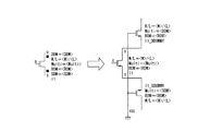
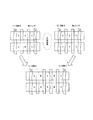
ここで、図2は、パラメータ設定可能なNMOSの回路シンボルの一例と、パラメータ設定後のマルチ素子回路のシンボル回路図の一例とを示す図である。
In the present embodiment, as a parameter automatically set by setting the above parameters, a column parameter (Column = <) in which a numerical value of a division result obtained by dividing the setting value of the parameter Multi by the setting value of the parameter ROW is set. Multi / ROW>).
Here, FIG. 2 is a diagram illustrating an example of an NMOS circuit symbol in which parameters can be set and an example of a symbol circuit diagram of a multi-element circuit after the parameters are set.
本実施の形態において、パラメータ設定が可能なNMOSの回路シンボルは、図2の左図に示すように、JISで標準化されているNMOSの回路シンボルの各端子部の傍に端子名G(Gate)、D(Drain)、S(Source)がそれぞれ表示され、更に、D端子の右側にパラメータ名「DDM(ドレイン端部側形成数)=<DDM>」と、S端子の右側にパラメータ名「SDM(ソース端部側形成数)=<SDM>」と、DDMとSDMの上下間に、パラメータ名「W(チャンネル幅)/L(チャンネル長)=<W>/<L>」と、パラメータ名「Multi(連続形成数)=<Multi>」と、パラメータ名「ROW=<ROW>」とが表示されたものとなる。パラメータ入力画面において、これらパラメータDDM、SDM、Multi、W/L、ROWにそれぞれ任意の数値を設定することで、マルチ素子回路を生成するためのパラメータ設定が行われる。 In this embodiment, as shown in the left diagram of FIG. 2, the NMOS circuit symbol whose parameters can be set is a terminal name G (Gate) beside each terminal portion of the NMOS circuit symbol standardized by JIS. , D (Drain), and S (Source) are displayed, and the parameter name “DDM (number of drain end side formations) = <DDM>” is displayed on the right side of the D terminal, and the parameter name “SDM” is displayed on the right side of the S terminal. (Number of source end side formations) = <SDM> ”, parameter name“ W (channel width) / L (channel length) = <W> / <L> ”and parameter name between the top and bottom of DDM and SDM “Multi (number of consecutive formations) = <Multi>” and the parameter name “ROW = <ROW>” are displayed. On the parameter input screen, by setting arbitrary numerical values for these parameters DDM, SDM, Multi, W / L, and ROW, parameter settings for generating a multi-element circuit are performed.
パラメータ判定部22は、パラメータ設定部20でパラメータ設定可能な回路シンボルに対して設定された設定内容が正しいか誤りかを、予め設定された正誤判定ルールに従って判定する機能を有している。
パラメータ修正部24は、パラメータ判定部22において、設定内容に誤りがあると判定されたときに、誤りのあった設定内容を、予め設定された修正ルールに従って修正する機能を有している。
The
The
更に、編集モード2において、回路パターン編集部14で編集された編集内容に基づき、編集された回路シンボルに対して設定されたパラメータを修正する機能を有している。
接続関係情報生成部26は、回路パターン編集部14でレイアウトされて構成された回路の接続関係情報を生成する機能と、予め設定されたルールに基づきパラメータ設定部20で設定されたパラメータに基づきマルチ素子回路の接続関係情報を生成する機能とを有している。生成された接続関係情報は、回路図情報記憶部28に記憶される。本実施の形態においては、更に、生成された接続関係情報のうちマルチ素子回路の接続関係情報は、回路表示情報生成部16に出力される。ここで、接続関係情報は、各回路素子(セル)の接続関係をテキストなどで表現した情報(ネットリストなど)である。
Further, in the
The connection relation
例えば、MOSトランジスタの回路シンボルに対してパラメータが設定された場合、予め設定されたルールに基づき、設定パラメータに応じた複数のMOSトランジスタとダミーMOSトランジスタとによって構成されるマルチ素子回路の各MOSトランジスタのゲート端子、ソース端子、ドレイン端子と他の回路素子(電源端子、接地端子などを含む)との接続関係が記述された接続関係情報が生成される。 For example, when a parameter is set for a circuit symbol of a MOS transistor, each MOS transistor of a multi-element circuit configured by a plurality of MOS transistors and a dummy MOS transistor according to a set parameter based on a preset rule The connection relationship information describing the connection relationship between the gate terminal, the source terminal, the drain terminal and other circuit elements (including the power supply terminal, the ground terminal, etc.) is generated.
なお、本実施の形態においては、NMOSのマルチ素子回路については、そのダミーNMOSのゲート端子を接地端子に接続すると共に、ダミーNMOSのNMOS本体部に接続されていない端子をフローティングにする接続関係情報を自動的に生成するルールが設定されている。更に、PMOSのマルチ素子回路については、そのダミーPMOSのゲート端子を電源端子に接続すると共に、ダミーPMOSのPMOS本体部に接続されていない端子をフローティングにする接続関係情報を自動的に生成するルールが設定されている。 In the present embodiment, for the NMOS multi-element circuit, connection information for connecting the gate terminal of the dummy NMOS to the ground terminal and floating the terminal not connected to the NMOS main body of the dummy NMOS is provided. A rule that automatically generates is set. Further, for a PMOS multi-element circuit, a rule for automatically generating connection relation information for connecting the gate terminal of the dummy PMOS to the power supply terminal and floating the terminal not connected to the PMOS main body of the dummy PMOS. Is set.
回路図情報記憶部28は、記憶装置(後述)の所定の記憶領域に構成されており、回路パターン編集部14によってレイアウトされた回路の情報や、接続関係情報生成部26で生成された接続関係情報などが記憶される。
以上の構成によって、回路図表示制御部18は、表示情報に基づき表示装置の表示制御を行ない、シンボル回路図又はパターンレイアウト図を表示装置の表示画面上に表示する。
The circuit diagram
With the above configuration, the circuit diagram
例えば、NMOSの回路シンボルに対してパラメータ設定をした場合のマルチ素子回路を示す回路シンボルは、図2の左図に示すように、本体NMOSの回路シンボルに対して、そのドレイン端子にダミーNMOSが接続されていることを示す■記号と、そのソース端子にダミーNMOSが接続されていることを示す■記号とが付加された回路シンボルが表示装置の表示画面上に表示される。 For example, a circuit symbol indicating a multi-element circuit when parameters are set for an NMOS circuit symbol is a dummy NMOS at the drain terminal of the main body NMOS circuit symbol as shown in the left diagram of FIG. A circuit symbol to which a ■ symbol indicating connection and a ■ symbol indicating that a dummy NMOS is connected to its source terminal is displayed on the display screen of the display device.
なお、図2の右図は、左図の回路シンボルに設定されたパラメータに基づき生成された接続関係情報を回路シンボルとパラメータ情報とによってイメージ化した回路図である。NMOSのマルチ素子回路は、本体NMOSの回路シンボルと、そのドレイン端子に接続されたダミーNMOSの回路シンボルと、そのソース端子に接続されたダミーNMOSの回路シンボルと、接地端子の回路シンボルとを含んで構成される回路図となる。 The right diagram in FIG. 2 is a circuit diagram in which connection relation information generated based on the parameters set in the circuit symbol in the left diagram is imaged by the circuit symbol and the parameter information. The NMOS multi-element circuit includes a body NMOS circuit symbol, a dummy NMOS circuit symbol connected to its drain terminal, a dummy NMOS circuit symbol connected to its source terminal, and a ground terminal circuit symbol. Is a circuit diagram composed of
具体的に、本体NMOSのドレイン及びソースにそれぞれダミーNMOSのドレイン及びソースがそれぞれ接続され、ダミーNMOSの本体NMOSに接続されていない端子はフローティング状態となり、ダミーNMOSのゲート端子は接地端子に接続されている。更に、各回路シンボルの右横には、各種パラメータ名と、その設定値とが表示されている。 Specifically, the drain and source of the dummy NMOS are connected to the drain and source of the main NMOS, respectively, the terminal not connected to the main NMOS of the dummy NMOS is in a floating state, and the gate terminal of the dummy NMOS is connected to the ground terminal. ing. Further, on the right side of each circuit symbol, various parameter names and their set values are displayed.
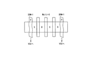
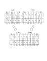
一方、NMOSの回路シンボルに対してパラメータ設定をした場合のマルチ素子回路のパターンレイアウト図は、図3に示すように、マスクシンボルによって形成された、本体NMOS(Multi=3)とダミーNMOS(DDM=1、SDM=1)のパターンレイアウトから構成されるパターンレイアウト図が表示装置の表示画面上に表示される。
ここで、図3は、NMOSで構成されたマルチ素子回路のパターンレイアウト図の一例を示す図である。
On the other hand, the pattern layout diagram of the multi-element circuit when parameters are set for the NMOS circuit symbol, as shown in FIG. 3, is the body NMOS (Multi = 3) and dummy NMOS (DDM) formed by the mask symbol. = 1, SDM = 1), a pattern layout diagram composed of the pattern layout is displayed on the display screen of the display device.
Here, FIG. 3 is a diagram showing an example of a pattern layout diagram of a multi-element circuit composed of NMOS.
具体的に、ダミーも含めたNMOS5つ分のソース領域とドレイン領域が同じ階層に行方向に交互に連続して形成され(隣り合う素子でソース領域とドレイン領域を共有)、更に、この階層よりも1つ上の階層における各ドレイン領域と各ソース領域との間の位置に各NMOSのゲート領域が形成された構成となっている。本体NMOS部は、中央の3つ分のNMOSから構成され、本体NMOS部の両端のNMOSが、それぞれダミーNMOSとなる。本実施の形態では、マルチ素子回路のパターンレイアウト図においてダミーNMOSが目視ですぐ判別できるようにするために、表示形状に関するルールに従って、そのゲート(図3中の「d」の付されたゲート)の形状を本体NMOS部のゲートの形状と異なる形状で表示している。 Specifically, source regions and drain regions for five NMOSs including a dummy are formed alternately and continuously in the row direction in the same hierarchy (the adjacent elements share the source region and the drain region). Also, the gate region of each NMOS is formed at a position between each drain region and each source region in the next higher layer. The main body NMOS unit is composed of three NMOSs in the center, and the NMOSs at both ends of the main body NMOS unit are dummy NMOSs. In the present embodiment, in order to allow the dummy NMOS to be immediately discriminated visually in the pattern layout diagram of the multi-element circuit, its gate (a gate indicated by “d” in FIG. 3) according to the rules regarding the display shape. Is shown in a shape different from the shape of the gate of the main body NMOS portion.
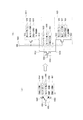
ここで、回路図設計装置100は、半導体集積回路に係る回路図の設計のための各種制御や前記回路記号選択部12、回路パターン編集部14、回路表示情報生成部16、回路図表示制御部18、パラメータ設定部20、パラメータ判定部22、パラメータ修正部24、接続関係情報生成部26などの各機能をソフトウェア上で、すなわち専用のプログラムを実行することで実現するためのコンピュータシステムを備えており、そのハードウェア構成は、図4に示すように、各種制御や演算処理を担う中央演算処理装置であるCPU(Central Processing Unit)60と、主記憶装置(Main Storage)を構成するRAM(Random Access Memory)62と、読み出し専用の記憶装置であるROM(Read Only Memory)64とを含み、これらの間をPCI(Peripheral Component Interconnect)バス等からなる各種内外バス68で接続すると共に、このバス68に入出力インターフェース(I/F)66を介して、HDD(Hard Disk Drive)などの記憶装置(Secondary Storage)70や、LCDモニター等の表示装置72、マウス、キーボード、タブレットなどの入力装置74などを接続した構成となっている。
Here, the circuit
そして、電源を投入すると、ROM64などに記憶されたBIOSなどのシステムプログラムが、ROM64に、予め記憶された各種専用のコンピュータプログラムを、あるいは、CD−ROMやDVD−ROM、フレキシブルディスク(FD)などの記録媒体を介して、またはインターネットなどの通信ネットワークLを介して、記憶装置70にインストールされた各種専用のコンピュータプログラムを、同じくRAM62にロードし、そのRAM62にロードされたプログラムに記述された命令に従ってCPU60が各種リソースを駆使して回路図の設計を実際に行うための各種制御及び演算処理を行うことで前述したような各部の機能をソフトウェア上で実現できるようになっている。
When the power is turned on, a system program such as BIOS stored in the
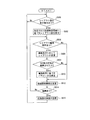
次に、図5に基づき、回路図設計装置100におけるマルチ素子回路の生成処理の流れを説明する。
ここで、図5は、マルチ素子回路の生成処理を示すフローチャートである。
CPU60によって、専用のコンピュータプログラムの実行が開始されると、図5に示すように、まず、ステップS100に移行し、回路記号選択部12において、入力装置74を介した利用者からの操作入力に基づき、回路シンボルの選択画面又はレイアウト領域にレイアウト(表示)されたシンボル回路図から、回路シンボルが選択されたか否かを判定し、選択されたと判定した場合(Yes)は、ステップS102に移行し、そうでない場合(No)は、選択されるまで判定処理を繰り返す。
Next, the flow of the multi-element circuit generation process in the circuit
Here, FIG. 5 is a flowchart showing a multi-element circuit generation process.
When the execution of the dedicated computer program is started by the
ステップS102に移行した場合は、パラメータ設定部20において、選択された回路シンボルがマルチ素子回路対応の回路シンボルか否かを判定し、対応の回路シンボルであると判定した場合(Yes)は、ステップS104に移行し、そうでない場合(No)は、ステップS100に移行する。
ステップS104に移行した場合は、パラメータ設定部20において、入力装置74を介した利用者からの操作入力に基づき、選択された回路シンボルに対してパラメータの入力指示があったか否かを判定し、入力指示があったと判定した場合(Yes)は、ステップS106に移行し、そうでない場合(No)は、ステップS100に移行する。
When the process proceeds to step S102, the
When the process proceeds to step S104, the
ステップS106に移行した場合は、パラメータ設定部20において、表示装置にパラメータの入力画面を表示させて、ステップS108に移行する。
このパラメータの入力画面は、例えば、選択された回路シンボルがMOSトランジスタであれば、本体MOSの連続形成数(Multi)、ダミーMOSの形成数(DDM,SDM)、各MOSのチャンネルサイズ(W/L)、マルチ素子回路の列方向の連続形成数(ROW)などのパラメータ設定項目と、各項目に対する数値入力用のボックスとが表示された画面となる。
When the process proceeds to step S106, the
For example, if the selected circuit symbol is a MOS transistor, the input screen for this parameter is the number of continuous formations of the main body MOS (Multi), the number of formations of the dummy MOSs (DDM, SDM), the channel size of each MOS (W / L), a screen on which parameter setting items such as the number of continuous formations (ROW) in the column direction of the multi-element circuit, and boxes for numerical input for each item are displayed.
ステップS108では、パラメータ判定部22において、パラメータの入力が完了したか否かを判定し、完了したと判定した場合(Yes)は、ステップS110に移行し、そうでない場合(No)は、パラメータの入力が完了するまで判定処理を繰り返す。
ステップS110に移行した場合は、パラメータ判定部22において、パラメータ判定処理を実行して、ステップS112に移行する。
In step S108, the
When the process proceeds to step S110, the
ステップS112では、パラメータ修正部24において、ステップS110の判定結果に基づき、設定値は正しいか否かを判定し、正しいと判定した場合(Yes)は、ステップS114に移行し、そうでない場合(No)は、ステップS122に移行する。
ステップS114に移行した場合は、接続関係情報生成部26において、選択された回路シンボルに対して設定されたパラメータに基づき、該回路シンボルの回路素子によって構成されるマルチ素子回路の接続関係情報を生成し、該生成した接続関係情報を回路表示情報生成部16に出力して、ステップS116に移行する。
In step S112, the
When the process proceeds to step S114, the connection relation
ステップS116では、回路表示情報生成部16において、マルチ素子回路の表示方法の決定処理を実行して、ステップS118に移行する。
ステップS118では、回路表示情報生成部16において、ステップS114で生成された接続関係情報と、ステップS116で決定された表示方法とに基づき、マルチ素子回路を示す回路シンボルの表示情報を生成し、これを表示要求と共に回路図表示制御部18に出力して、ステップS120に移行する。
In step S116, the circuit display
In step S118, the circuit display
ステップS120では、回路図表示制御部18において、表示情報に基づき、表示装置に、選択した回路シンボルに対するマルチ素子回路を示す回路シンボルを表示させて、ステップS100に移行する。
なお、本実施の形態においては、回路表示情報生成部16に対して、選択した回路シンボルに対するマルチ素子回路を示すパターンレイアウト図の表示指示を行うことができる。この表示指示を行うことによって、回路表示情報生成部16は、ステップS114で生成された接続関係情報と、ステップS116で決定された表示方法とに基づき、マルチ素子回路のパターンレイアウト図の表示情報を生成し、回路図表示制御部18は、この表示情報に基づき、レイアウト領域内又は別ウィンドウにマルチ素子回路のパターンレイアウト図を表示する。
In step S120, the circuit diagram
In the present embodiment, it is possible to instruct the circuit display
一方、ステップS112において、パラメータの設定値が正しくない(誤り)と判定され、ステップS122に移行した場合は、パラメータ修正部24において、パラメータ修正処理を実行して誤った設定値を修正し、ステップS114に移行する。
On the other hand, if it is determined in step S112 that the parameter setting value is not correct (error) and the process proceeds to step S122, the
次に、図6に基づき、回路図設計装置100のパラメータ判定部22におけるステップS110のパラメータ判定処理の流れを説明する。
ここで、図6は、パラメータ判定部22におけるMOSトランジスタの回路シンボルに対するパラメータ判定処理の一例を示すフローチャートである。
ステップS110に移行し、パラメータ判定処理が開始されると、図6に示すように、まず、ステップS200に移行し、パラメータ判定部22において、パラメータROWの値は「2」以上か否かを判定し、「2」以上であると判定した場合(Yes)は、ステップS202に移行し、そうでない場合(No)は、ステップS220に移行する。
Next, based on FIG. 6, the flow of the parameter determination process in step S110 in the
FIG. 6 is a flowchart showing an example of parameter determination processing for the circuit symbol of the MOS transistor in the
When the process proceeds to step S110 and the parameter determination process is started, as shown in FIG. 6, first, the process proceeds to step S200, where the
ステップS202に移行した場合は、パラメータ判定部22において、パラメータMultiの設定値をパラメータROWの設定値で除算して、ステップS204に移行する。
ステップS204では、パラメータ判定部22において、ステップS202の除算結果は割り切れた値か否かを判定し、割り切れた値であると判定した場合(Yes)は、ステップS206に移行し、そうでない場合(No)は、ステップS218に移行する。
When the process proceeds to step S202, the
In step S204, the
ステップS206に移行した場合は、パラメータ判定部22において、パラメータColumnに、ステップS202の除算結果を設定して、ステップS208に移行する。
ステップS208では、パラメータ判定部22において、パラメータColumnの設定値は奇数か否かを判定し、奇数であると判定した場合(Yes)は、ステップS210に移行し、そうでない場合(No)は、ステップS216に移行する。
When the process proceeds to step S206, the
In step S208, the
ステップS210に移行した場合は、パラメータDDM又はSDMに、パラメータROWの設定をN倍(Nは1以上の整数)した数値とは異なる値が設定されているか否かを判定し、設定されていると判定した場合(Yes)は、ステップS212に移行し、そうでない場合(No)は、ステップS214に移行する。
ステップS212に移行した場合は、パラメータ判定部22において、第4の設定内容による誤りと判定し、該判定結果をパラメータ修正部24に出力して、一連の処理を終了し元の処理に復帰する。
When the process proceeds to step S210, it is determined whether or not the parameter DDM or SDM is set to a value different from the value obtained by multiplying the parameter ROW by N (N is an integer of 1 or more). If determined (Yes), the process proceeds to step S212. If not (No), the process proceeds to step S214.
When the process proceeds to step S212, the
一方、ステップS214に移行した場合は、パラメータ判定部22において、設定値は正しいと判定し、該判定結果をパラメータ修正部24に出力して、一連の処理を終了し元の処理に復帰する。
また、ステップS208において、パラメータColumnの設定値が偶数で、ステップS216に移行した場合は、パラメータ判定部22において、パラメータDDM又はSDMに、パラメータROWの設定値をM倍(Mは2以上の偶数)した値とは異なる値が設定されているか否かを判定し、設定されていると判定した場合(Yes)は、ステップS218に移行し、そうでない場合(No)は、ステップS214に移行する。
On the other hand, when the process proceeds to step S214, the
In step S208, when the setting value of the parameter Column is an even number and the process proceeds to step S216, the
ステップS218に移行した場合は、パラメータ判定部22において、第5の設定内容による誤りと判定し、該判定結果をパラメータ修正部24に出力して、一連の処理を終了し元の処理に復帰する。
一方、ステップS204において、ステップS202の除算結果が割り切れずにステップS220に移行した場合は、パラメータColumnに除算結果の小数部分を切り捨てた値を設定して、ステップS208に移行する。
When the process proceeds to step S218, the
On the other hand, in step S204, if the division result in step S202 is not divisible and the process proceeds to step S220, the value obtained by rounding off the decimal part of the division result is set in the parameter Column, and the process proceeds to step S208.
また、ステップS200において、パラメータROWの設定値が1で(本実施の形態では1未満の数値は設定禁止とする)、ステップS222に移行した場合は、パラメータ判定部22において、パラメータMultiが偶数で且つ本体MOS部の両端はソース領域か否かを判定し、偶数且つソース領域であると判定した場合(Yes)は、ステップS224に移行し、そうでない場合(No)は、ステップS232に移行する。
In step S200, when the setting value of the parameter ROW is 1 (a numerical value less than 1 is prohibited in this embodiment) and the process proceeds to step S222, the
ステップS224に移行した場合は、パラメータDDM及びSDMの双方に「0」以外の数値が設定されているか否かを判定し、設定されていると判定した場合(Yes)は、ステップS226に移行し、そうでない場合(No)は、ステップS228に移行する。
ステップS226に移行した場合は、パラメータ判定部22において、第1の設定内容による誤りと判定し、該判定結果をパラメータ修正部24に出力して、一連の処理を終了し元の処理に復帰する。
When the process proceeds to step S224, it is determined whether or not a numerical value other than “0” is set in both parameters DDM and SDM. If it is determined that the parameter is set (Yes), the process proceeds to step S226. If not (No), the process proceeds to step S228.
When the process proceeds to step S226, the
一方、ステップS228に移行した場合は、パラメータ判定部22において、パラメータDDMに「0」が設定され、パラメータSDMに所定の偶数値が設定されているか否かを判定し、設定されていると判定した場合(Yes)は、ステップS214に移行し、そうでない場合(No)は、ステップS230に移行する。
ステップS230に移行した場合は、パラメータ判定部22において、第2の設定内容による誤りと判定し、該判定結果をパラメータ修正部24に出力して、一連の処理を終了し元の処理に復帰する。
On the other hand, when the process proceeds to step S228, the
When the process proceeds to step S230, the
また、ステップS222において、パラメータMultiが奇数又は両端部がソース領域じゃなくてステップS232に移行した場合は、パラメータ判定部22において、パラメータMultiが偶数で且つ本体MOS部の両端はドレイン領域か否かを判定し、偶数且つドレイン領域であると判定した場合(Yes)は、ステップS234に移行し、そうでない場合(No)は、ステップS214に移行する。
In step S222, if the parameter Multi is odd or both ends are not the source region and the process proceeds to step S232, the
ステップS234に移行した場合は、パラメータ判定部22において、パラメータDDM及びSDMの双方に「0」以外の数値が設定されているか否かを判定し、設定されていると判定した場合(Yes)は、ステップS226に移行し、そうでない場合(No)は、ステップS236に移行する。
ステップS236に移行した場合は、パラメータ判定部22において、パラメータSDMに「0」が設定され、パラメータDDMに所定の偶数値が設定されているか否かを判定し、設定されていると判定した場合(Yes)は、ステップS214に移行し、そうでない場合(No)は、ステップS238に移行する。
When the process proceeds to step S234, the
When the process proceeds to step S236, the
ステップS238に移行した場合は、パラメータ判定部22において、第3の設定内容による誤りと判定し、該判定結果をパラメータ修正部24に出力して、一連の処理を終了し元の処理に復帰する。
When the process proceeds to step S238, the
次に、図7に基づき、回路図設計装置100のパラメータ修正部24におけるステップS122のパラメータ修正処理の流れを説明する。
ここで、図7は、パラメータ修正部24における、MOSトランジスタに対するパラメータ修正処理を示すフローチャートである。
ステップS122に移行し、パラメータ修正処理が開始されると、図7に示すように、まず、ステップS300に移行し、パラメータ修正部24において、ステップS112の判定結果が第1の設定内容による誤り判定か否かを判定し、そうである場合(Yes)は、ステップS302に移行し、そうでない場合(No)は、ステップS308に移行する。
Next, the flow of the parameter correction process in step S122 in the
FIG. 7 is a flowchart showing parameter correction processing for the MOS transistor in the
When the process proceeds to step S122 and the parameter correction process is started, as shown in FIG. 7, the process first proceeds to step S300. If it is (Yes), the process proceeds to step S302. If not (No), the process proceeds to step S308.
ステップS302に移行した場合は、パラメータ修正部24において、本体MOS部の両端がソース領域か否かを判定し、そうである場合(Yes)は、ステップS304に移行し、そうでない場合(No)は、ステップS306に移行する。
ステップS304に移行した場合は、パラメータ修正部24において、パラメータDDMが「0」に且つパラメータSDMが所定の偶数値となるように修正して、一連の処理を終了し元の処理に復帰する。
When the process proceeds to step S302, the
When the process proceeds to step S304, the
一方、ステップS306に移行した場合は、パラメータ修正部24において、パラメータDDMが所定の偶数値に且つパラメータSDMが「0」となるように修正して、一連の処理を終了し元の処理に復帰する。
また、ステップS300において、第1の設定内容による誤り判定ではなく、ステップS308に移行した場合は、パラメータ修正部24において、ステップS112の判定結果が第2の設定内容による誤り判定か否かを判定し、そうである場合(Yes)は、ステップS310に移行し、そうでない場合(No)は、ステップS312に移行する。
On the other hand, when the process proceeds to step S306, the
Also, in step S300, if the error determination based on the first setting content is not performed but the process proceeds to step S308, the
ステップS310に移行した場合は、パラメータ修正部24において、パラメータSDMの設定値を所定の偶数値に修正して、一連の処理を終了し元の処理に復帰する。
一方、ステップS312に移行した場合は、パラメータ修正部24において、ステップS112の判定結果が第3の設定内容による誤り判定か否かを判定し、そうであると判定した場合(Yes)は、ステップS314に移行し、そうでない場合(No)は、ステップS316に移行する。
When the process proceeds to step S310, the
On the other hand, when the process proceeds to step S312, the
ステップS314に移行した場合は、パラメータ修正部24において、パラメータDDMを所定の偶数値に修正して、一連の処理を終了し元の処理に復帰する。
また、ステップS316に移行した場合は、パラメータ修正部24において、ステップS112の判定結果が第4の設定内容による誤り判定か否かを判定し、そうであると判定した場合(Yes)は、ステップS318に移行し、そうでない場合(No)は、ステップS320に移行する。
When the process proceeds to step S314, the
If the process proceeds to step S316, the
ステップS318に移行した場合は、パラメータ修正部24において、パラメータDDM及びSDMの設定値が双方ともROWの設定値をN倍にした数値となるようにこれら設定値を修正して、一連の処理を終了し元の処理に復帰する。
一方、ステップS320に移行した場合は、パラメータ修正部24において、本体MOS部の両端がソース領域か否かを判定し、そうである場合(Yes)は、ステップS322に移行し、そうでない場合(No)は、ステップS324に移行する。
When the process proceeds to step S318, the
On the other hand, when the process proceeds to step S320, the
ステップS322に移行した場合は,パラメータ修正部24において、パラメータDDMの設定値が「0」に且つパラメータSDMの設定値がパラメータROWの設定値をM倍した数値となるようにこれら設定値を修正して、一連の処理を終了し元の処理に復帰する。
また、ステップS324に移行した場合は、パラメータ修正部24において、パラメータSDMの設定値が「0」に且つパラメータDDMの設定値がパラメータROWの設定値をM倍した数値となるようにこれら設定値を修正して、一連の処理を終了し元の処理に復帰する。
When the process proceeds to step S322, the
When the process proceeds to step S324, the
次に、図8に基づき、回路図設計装置100の接続関係情報生成部26におけるステップS114の接続関係情報生成処理の流れを説明する。
ここで、図8は、接続関係情報生成部26における、MOSトランジスタに対する接続関係情報生成処理の一例を示すフローチャートである。
ステップS114に移行し、接続関係情報生成処理が開始されると、図8に示すように、まず、ステップS400に移行し、接続関係情報生成部26において、パラメータROWの設定値が「2」以上であるか否かを判定し、「2」以上であると判定した場合(Yes)は、ステップS402に移行し、そうでない場合(No)は、ステップS404に移行する。
Next, based on FIG. 8, the flow of the connection relationship information generation process of step S114 in the connection relationship
Here, FIG. 8 is a flowchart showing an example of connection relationship information generation processing for the MOS transistor in the connection relationship
When the process proceeds to step S114 and the connection relation information generation process is started, as shown in FIG. 8, first, the process proceeds to step S400, and the connection relation
ステップS402に移行した場合は、パラメータMulti、DDM、SDMの設定値をパラメータROWの設定値で除算した数値を、以降の接続関係生成処理に用いる各パラメータ値として設定して、ステップS404に移行する。
ステップS404では、接続関係情報生成部26において、パラメータDDMが「0」で且つパラメータSDMが「0」であるか否かを判定し、双方が「0」であると判定した場合(Yes)は、ステップS406に移行し、そうでない場合(No)は、ステップS414に移行する。
When the process proceeds to step S402, a numerical value obtained by dividing the setting values of the parameters Multi, DDM, and SDM by the setting value of the parameter ROW is set as each parameter value used for the subsequent connection relationship generation processing, and the process proceeds to step S404. .
In step S404, the connection relation
ステップS406に移行した場合は、接続関係情報生成部26において、パラメータMultiの値に基づき、ダミーMOS無しの本体MOS部のみのマルチ素子回路の接続関係情報を生成してRAM62に記憶し、ステップS408に移行する。
ステップS408では、接続関係情報生成部26において、パラメータROWの設定値が「2」以上であるか否かを判定し、「2」以上であると判定した場合(Yes)は、ステップS410に移行し、そうでない場合(No)は、ステップS412に移行する。
When the process proceeds to step S406, the connection relation
In step S408, the connection relationship
ステップS410に移行した場合は、接続関係情報生成部26において、パラメータROWの設定値に基づきRAM62に記憶された接続関係情報をマルチ素子回路列を構成する接続関係情報に補正して、ステップS412に移行する。
ステップS412では、接続関係情報生成部26において、生成した接続関係情報を、回路表示情報生成部16に出力すると共に回路図情報記憶部28に保存して、一連の処理を終了し元の処理に復帰する。
When the process proceeds to step S410, the connection relation
In step S412, the connection relation
一方、ステップS404において、パラメータSDM及びDDMの設定値の双方が「0」でなく、ステップS414に移行した場合は、接続関係情報生成部26において、選択された回路シンボルが、PMOSか否かを判定し、PMOSであると判定した場合(Yes)は、ステップS416に移行し、そうでない場合(No)は、ステップS430に移行する。
ステップS416に移行した場合は、接続関係情報生成部26において、パラメータMultiの設定値<Multi>に基づき、ダミーPMOSを付加していない状態の、<Multi>個のPMOSが連続して接続された構成の本体PMOS部だけのマルチ素子回路の接続関係情報を生成してRAM62に記憶し、ステップS418に移行する。
On the other hand, if both the setting values of the parameters SDM and DDM are not “0” in step S404 and the process proceeds to step S414, the connection relation
When the process proceeds to step S416, in the connection relation
ステップS418では、接続関係情報生成部26において、パラメータDDMの設定値は「1」以上か否かを判定し、「1」以上であると判定した場合(Yes)は、ステップS420に移行し、そうでない場合(No)は、ステップS422に移行する。
ステップS420に移行した場合は、接続関係情報生成部26において、パラメータDDMの設定値に基づき、本体PMOS部のドレイン端部にダミーPMOSを接続する情報を、RAM62に記憶された接続関係情報に追加して、ステップS422に移行する。
In step S418, the connection relation
When the process proceeds to step S420, the connection relation
ステップS422では、接続関係情報生成部26において、パラメータSDMの設定値は「1」以上か否かを判定し、「1」以上であると判定した場合(Yes)は、ステップS424に移行し、そうでない場合(No)は、ステップS426に移行する。
ステップS424に移行した場合は、接続関係情報生成部26において、本体PMOS部のソース端部にダミーPMOSを接続する情報を、RAM62に記憶された接続関係情報に追加して、ステップS426に移行する。
In step S422, the connection relation
When the process proceeds to step S424, the connection relation
ステップS426では、接続関係情報生成部26において、ダミーPMOSのゲート端子を電源端子に接続する情報を、RAM62に記憶された接続関係情報に追加して、ステップS428に移行する。
ステップS428では、接続関係情報生成部26において、ダミーPMOS又はダミーNMOSの接続されていない端子をフローティングにする情報を、RAM62に記憶された接続関係情報に追加して、ステップS408に移行する。
In step S426, the connection relation
In step S428, in the connection relation
一方、ステップS414において、選択された回路シンボルがPMOSではなくてNMOSであり、ステップS430に移行した場合は、接続関係情報生成部26において、パラメータMultiの設定値<Multi>に基づき、ダミーNMOSを付加していない状態の、<Multi>個のNMOSが連続して接続された構成の本体NMOS部だけのマルチ素子回路の接続関係情報を生成してRAM62に記憶し、ステップS432に移行する。
On the other hand, if the selected circuit symbol is not PMOS but NMOS in step S414 and the process proceeds to step S430, the connection relation
ステップS432では、接続関係情報生成部26において、パラメータDDMの設定値は「1」以上か否かを判定し、「1」以上であると判定した場合(Yes)は、ステップS434に移行し、そうでない場合(No)は、ステップS436に移行する。
ステップS434に移行した場合は、接続関係情報生成部26において、パラメータDDMの設定値に基づき、本体NMOS部のドレイン端部にダミーNMOSを接続する情報を、RAM62に記憶された接続関係情報に追加して、ステップS436に移行する。
In step S432, the connection relation
When the process proceeds to step S434, the connection relation
ステップS436では、接続関係情報生成部26において、パラメータSDMの設定値は「1」以上か否かを判定し、「1」以上であると判定した場合(Yes)は、ステップS438に移行し、そうでない場合(No)は、ステップS440に移行する。
ステップS438に移行した場合は、接続関係情報生成部26において、本体NMOS部のソース端部にダミーNMOSを接続する情報を、RAM62に記憶された接続関係情報に追加して、ステップS440に移行する。
In step S436, the connection relation
When the process proceeds to step S438, the connection relation
ステップS440では、接続関係情報生成部26において、ダミーNMOSのゲート端子を電源端子に接続する情報を、RAM62に記憶された接続関係情報に追加して、ステップS428に移行する。
なお、上記生成されたマルチ素子回路の接続関係情報は、最終的に、レイアウト領域にレイアウトされた回路全体の接続関係情報における、対応する回路シンボルに対応付けられて回路図情報記憶部28に保存されるか、回路全体の接続関係情報における、対応する回路シンボルの接続関係情報を置き換えて回路図情報記憶部28に保存される。
In step S440, the connection relation
The generated connection relationship information of the multi-element circuit is finally stored in the circuit diagram
次に、図9に基づき、回路図設計装置100の回路表示情報生成部16におけるステップ116の、回路シンボルの表示方法を決定する処理である表示方法決定処理の流れを説明する。
ここで、図9は、回路表示情報生成部16における表示方法決定処理を示すフローチャートである。
Next, based on FIG. 9, the flow of the display method determination process, which is the process of determining the circuit symbol display method, in step 116 in the circuit display
Here, FIG. 9 is a flowchart showing a display method determination process in the circuit display
ステップS116に移行し、表示方法決定処理が開始されると、図9に示すように、まず、ステップS500に移行し、回路表示情報生成部16において、表示形状に関するルールがあるか否かを判定し、表示形状に関するルールがあると判定した場合(Yes)は、ステップS502に移行し、そうでない場合(No)は、ステップS504に移行する。
ステップS502に移行した場合は、回路表示情報生成部16において、表示形状に関するルールに基づきマルチ素子回路の回路シンボルの表示形状を決定して、ステップS504に移行する。
When the process proceeds to step S116 and the display method determination process is started, as shown in FIG. 9, first, the process proceeds to step S500, and the circuit display
When the process proceeds to step S502, the circuit display
ステップS504では、回路表示情報生成部16において、表示色に関するルールがあるか否かを判定し、表示色に関するルールがあると判定した場合(Yes)は、ステップS506に移行し、そうでない場合(No)は、一連の処理を終了し元の処理に復帰する。
ステップS506に移行した場合は、回路表示情報生成部16において、表示色に関するルールに基づき、マルチ素子回路の回路シンボルの表示色を決定して、一連の処理を終了し元の処理に復帰する。
In step S504, the circuit display
When the process proceeds to step S506, the circuit display
次に、図10に基づき、回路図設計装置100におけるパターンレイアウト図の編集処理の流れを説明する。
ここで、図10は、回路図設計装置100におけるパターンレイアウト図の編集処理を示すフローチャートである。
CPU60によって専用のプログラムが実行され、パターンレイアウト図の編集処理が開始されると、図10に示すように、まず、ステップS600に移行し、回路表示情報生成部16において、入力装置74を介した利用者からの指定接続関係情報のパターンレイアウト図の表示指示があったか否かを判定し、あったと判定した場合(Yes)は、回路表示情報生成部16において、指定接続関係情報に基づき、そのパターンレイアウト図の表示情報を生成し、該生成した表示情報を表示要求と共に回路図表示制御部18に出力する。更に、回路図表示制御部18において、入力された表示情報に基づき表示装置72を制御して、表示画面上にパターンレイアウト図を表示して、ステップS604に移行する。
Next, the flow of the pattern layout diagram editing process in the circuit
Here, FIG. 10 is a flowchart showing the editing process of the pattern layout diagram in the circuit
When the dedicated program is executed by the
ステップS604では、回路パターン編集部14において、入力装置74を介した利用者からのレイアウト編集指示があったか否かを判定し、あったと判定した場合(Yes)は、ステップS606に移行し、そうでない場合(No)は、ステップS614に移行する。
本実施の形態において、編集指示内容としては、具体的に、パターンレイアウト図における、マルチ素子回路又は複数のマルチ素子回路列の列数の変更指示、マルチ素子回路又はマルチ素子回路列の各本体MOS部の連続形成数の変更指示、マルチ素子回路を構成するMOSトランジスタのPMOSからNMOSへ又はNMOSからPMOSへのいずれかへの変換指示、複数のマルチ素子回路又は複数のマルチ素子回路列の共有合成指示、複数のマルチ素子回路又は複数のマルチ素子回路列の所定合体構成(例えば、コモン・セントロイドなど)の合体合成指示などが可能である。
In step S604, the circuit
In the present embodiment, the editing instruction content specifically includes an instruction to change the number of columns of a multi-element circuit or a plurality of multi-element circuit columns in the pattern layout diagram, and each main body MOS of the multi-element circuit or multi-element circuit column. Instructions for changing the number of continuous formation of parts, instructions for conversion of MOS transistors constituting a multi-element circuit from either PMOS to NMOS or NMOS to PMOS, shared synthesis of multiple multi-element circuits or multiple multi-element circuit arrays An instruction, an instruction for merging and synthesizing a predetermined merging configuration (for example, a common centroid, etc.) of a plurality of multi-element circuits or a plurality of multi-element circuit arrays can be performed.
ステップS606に移行した場合は、回路パターン編集部14、回路表示情報生成部16、回路図表示制御部18において、編集指示に応じてパターンレイアウト図のレイアウトを変更して、ステップS608に移行する。
ステップS608では、パラメータ修正部24において、ステップS606の編集結果に基づき、マルチ素子回路が編集されたか否かを判定し、編集されたと判定した場合(Yes)は、ステップS610に移行し、そうでない場合(No)は、ステップS612に移行する。
When the process proceeds to step S606, the circuit
In step S608, the
ステップS610に移行した場合は、パラメータ修正部24において、ステップS606の編集結果に基づき、編集された回路シンボルに対するパラメータを修正して、ステップS612に移行する。
ステップS612では、接続関係情報生成部26において、ステップS606の編集結果及びステップS610のパラメータ修正結果に基づき接続関係情報を変更して、ステップS614に移行する。
When the process proceeds to step S610, the
In step S612, the connection relation
ステップS614では、回路図設計装置100において、パターンレイアウト図の編集処理の終了指示があったか否かを判定し、あったと判定した場合(Yes)は、ステップS616に移行し、そうでない場合(No)は、ステップS604に移行する。
ステップS616に移行した場合は、接続関係情報生成部26において、編集内容の反映された接続関係情報、パラメータ設定値などの回路図の情報を回路図情報記憶部28に記憶して、ステップS600に移行する。
In step S614, the circuit
When the process proceeds to step S616, the connection relationship
次に、図11に基づき、パターンレイアウト図の編集処理における、ステップS610のパラメータ修正処理の流れを説明する。
ここで、図11は、パラメータ修正部24の、パターンレイアウト図におけるMOSトランジスタのマルチ素子回路の編集処理に対するパラメータ修正処理の一例を示すフローチャートである。
Next, the flow of parameter correction processing in step S610 in the pattern layout diagram editing processing will be described with reference to FIG.
Here, FIG. 11 is a flowchart showing an example of parameter correction processing for the editing processing of the multi-element circuit of the MOS transistor in the pattern layout diagram of the
ステップS610に移行し、パターンレイアウト図におけるMOSトランジスタのマルチ素子回路の編集処理に対するパラメータ修正処理が開始されると、図11に示すように、まず、ステップS700に移行し、回路パターン編集部14において、MOSトランジスタから構成されたマルチ素子回路の列数が変更されたか否かを判定し、変更されたと判定した場合(Yes)は、その編集内容をパラメータ修正部24に通知して、ステップS706に移行し、そうでない場合(No)は、ステップS726に移行する。
When the process proceeds to step S610 and the parameter correction process for the edit process of the multi-element circuit of the MOS transistor in the pattern layout diagram is started, first, the process proceeds to step S700 as shown in FIG. Then, it is determined whether or not the number of columns of the multi-element circuit composed of MOS transistors has been changed. If it is determined that the number has been changed (Yes), the
ステップS706では、パラメータColumnの設定値は奇数か否かを判定し、奇数であると判定した場合(Yes)は、ステップS708に移行し、そうでない場合(No)は、ステップS710に移行する。
ステップS708に移行した場合は、パラメータ修正部24において、パラメータDDM及びSDMの設定値を、修正後のパラメータROWの設定値をN倍した数値に修正して、一連の処理を終了し元の処理に復帰する。
In step S706, it is determined whether or not the setting value of the parameter Column is an odd number. If it is determined that it is an odd number (Yes), the process proceeds to step S708, and if not (No), the process proceeds to step S710.
When the process proceeds to step S708, the
一方、ステップS710に移行した場合は、パラメータ修正部24において、本体MOS部の両端部はソース領域か否かを判定し、ソース領域であると判定した場合(Yes)は、ステップS712に移行し、そうでない場合(No)は、ステップS720に移行する。
ステップS712に移行した場合は、パラメータ修正部24において、パラメータDDMの設定値は「0」か否かを判定し、「0」であると判定した場合(Yes)は、ステップS714に移行し、そうでない場合(No)は、ステップS716に移行する。
On the other hand, when the process proceeds to step S710, the
When the process proceeds to step S712, the
ステップS714に移行した場合は、パラメータ修正部24において、パラメータSDMの設定値を、修正後のパラメータROWの設定値をM倍した数値に修正して、一連の処理を終了し元の処理に復帰する。
また、ステップS716に移行した場合は、パラメータ修正部24において、パラメータDDMの設定値を「0」に且つパラメータSDMの設定値を、修正後のパラメータROWの設定値をM倍した数値に修正して、一連の処理を終了し元の処理に復帰する。
When the process proceeds to step S714, the
When the process proceeds to step S716, the
また、ステップS710において、本体MOS部の両端がドレイン領域であり、ステップS720に移行した場合は、パラメータ修正部24において、パラメータSDMの設定値は「0」であるか否かを判定し、「0」であると判定した場合(Yes)は、ステップS722に移行し、そうでない場合(No)は、ステップS724に移行する。
ステップS722に移行した場合は、パラメータ修正部24において、パラメータDDMの設定値を、修正後のパラメータROWの設定値をM倍した数値に修正して、一連の処理を終了し元の処理に復帰する。
In step S710, both ends of the main body MOS unit are drain regions. When the process proceeds to step S720, the
When the process proceeds to step S722, the
一方、ステップS724に移行した場合は、パラメータ修正部24において、パラメータSDMの設定値を「0」に且つパラメータDDMの設定値を、修正後のパラメータROWの設定値をM倍した数値に修正して、一連の処理を終了し元の処理に復帰する。
また、ステップS700において、マルチ素子回路の列数が変更されずに、マルチ素子回路の供給合成処理が行われたか否かを判定し、行われたと判定した場合(Yes)は、ステップS728に移行し、そうでない場合(No)は、ステップS730に移行する。
On the other hand, when the process proceeds to step S724, the
In step S700, it is determined whether the multi-element circuit supply / synthesis processing has been performed without changing the number of columns of the multi-element circuit. If it is determined (Yes), the process proceeds to step S728. If not (No), the process proceeds to step S730.
ステップS728に移行した場合は、パラメータ修正部24において、第1〜第nのマルチ素子回路又はマルチ素子回路列のパラメータDDM及びSDMの設定値を、共有数に応じて減らす修正を行い、一連の処理を終了し元の処理に復帰する。
一方、ステップS730に移行した場合は、パラメータ修正部24において、合体合成処理を行われたか否かを判定し、行われたと判定した場合(Yes)は、ステップS732に移行し、そうでない場合(No)は、マルチ素子回路への他の編集内容に基づき、パラメータの設定値を修正して、一連の処理を終了し元の処理に復帰する。
When the process proceeds to step S728, the
On the other hand, when the process proceeds to step S730, the
ステップS732に移行した場合は、パラメータ修正部24において、合体方法に基づき、第1〜第nのマルチ素子回路に対するパラメータSDM及びDDMの値を再計算して、ステップS734に移行する。
ステップS734では、パラメータ修正部24において、ステップS732の再計算結果に基づき、各マルチ素子回路のパラメータSDM及びDDMの設定値を修正して、一連の処理を終了し元の処理に復帰する。
When the process proceeds to step S732, the
In step S734, the
次に、図12〜図18に基づき、本実施の形態の回路図設計装置100のより具体的な動作を説明する。
ここで、図12(a)は、NMOSの回路シンボルの一例を示す図であり、(b)は、(a)の回路シンボルに対するパラメータ入力画面の一例を示す図である。また、図13(a)〜(d)は、パラメータの設定されたNMOSの回路シンボルの表示形状の例を示す図である。また、図14(a)〜(c)は、パラメータMultiの値を「4」にしたときのマルチ素子回路のパターンレイアウト図の例を示す図である。また、図15(a)は、パラメータ設定可能なPMOSの回路シンボルの一例を示す図であり、(b)は、(a)の回路シンボルに対するマルチ素子回路の回路構成の一例を示す図である。また、図16(a)は、パラメータ入力画面の一例を示す図であり、(b)は、パラメータROWの値を「2」にしたときのマルチ素子回路のパターンレイアウト図の一例を示す図である。また、図17は、マルチ素子回路の共有合成の一例を示す図である。また、図18は、マルチ素子回路の合体合成の一例を示す図である。
Next, a more specific operation of the circuit
Here, FIG. 12A is a diagram illustrating an example of an NMOS circuit symbol, and FIG. 12B is a diagram illustrating an example of a parameter input screen for the circuit symbol of FIG. FIGS. 13A to 13D are diagrams showing examples of display shapes of NMOS circuit symbols in which parameters are set. FIGS. 14A to 14C are diagrams showing examples of pattern layout diagrams of the multi-element circuit when the value of the parameter Multi is “4”. FIG. 15A is a diagram illustrating an example of a PMOS circuit symbol whose parameters can be set, and FIG. 15B is a diagram illustrating an example of a circuit configuration of a multi-element circuit with respect to the circuit symbol of FIG. . FIG. 16A is a diagram showing an example of a parameter input screen, and FIG. 16B is a diagram showing an example of a pattern layout diagram of a multi-element circuit when the value of the parameter ROW is “2”. is there. FIG. 17 is a diagram illustrating an example of shared synthesis of multi-element circuits. FIG. 18 is a diagram showing an example of the combined synthesis of multi-element circuits.
回路図設計装置100に電源が投入され、専用のプログラムが実行されると半導体集積回路に係る回路図の設計処理が開始される。これにより、利用者は、入力装置74を介して各種指示を与えることで、半導体集積回路に係る新規回路図の作成処理、既に作成した回路図の変更、修正などの編集処理などを行うことで回路図の設計を行うことができる。
いま、入力装置74を介して利用者からの、既に作成された接続関係情報に対する回路図の表示指示があったとする。回路表示情報生成部16は、表示指示(接続関係情報の指定及び図の表示形式の指定を含む)に応じて、回路図情報記憶部28から、指定された接続関係情報を読み出し、指示に応じた表示形態の回路図(シンボル回路図又はパターンレイアウト図)の表示情報を生成する。
When power is turned on to the circuit
Now, it is assumed that there is a circuit diagram display instruction for the connection relation information already created from the user via the
回路表示情報生成部16は、生成した表示情報を表示要求と共に回路図表示制御部18に出力する。これによって、表示装置72の表示画面上に表示されたレイアウト領域に、指定された接続関係情報に対する指定された表示形態の回路図が表示され、編集モード1又は2へと移行する。
ここでは、MOSトランジスタの回路シンボルを含む複数種類の回路シンボル及び配線パターンによって表されたシンボル回路図が表示され、編集モード1に移行したとする。
The circuit display
Here, it is assumed that a plurality of types of circuit symbols including circuit symbols of MOS transistors and symbol circuit diagrams represented by wiring patterns are displayed, and the mode is shifted to the
そして、入力装置74を介した操作入力に基づき、表示されたシンボル回路図を構成する回路シンボルの中から、図12(a)に示す、NMOSの回路シンボルが選択されると(ステップS100の「Yes」の分岐)、パラメータ設定部20において、該選択されたNMOSの回路シンボルがマルチ素子回路に対応しているか否かを判定する。
ここで、NMOSの回路シンボルは、図12(a)に示すように、NMOS本体部0800と、第1〜第5パラメータ表示領域0804〜0808とを含んで構成されている。
When an NMOS circuit symbol shown in FIG. 12A is selected from the circuit symbols constituting the displayed symbol circuit diagram based on the operation input via the input device 74 (“S” in step S100). In the “Yes” branch), the
Here, the NMOS circuit symbol includes an NMOS
NMOS本体部0800は、ゲート端子0801と、ドレイン端子0802と、ソース端子0803とを含んで構成されている。
第1のパラメータ表示領域0804は、NMOS本体部のドレインに付加するダミーNMOSの数を示すパラメータ情報「DDM=<DDM>」を表示する領域であり、第4パラメータ表示領域0807は、NMOS本体部のソースに付加するダミーNMOSの数を示すパラメータ情報「SDM=<SDM>」を表示する領域である。ここで、<DDM>、<SDM>には入力装置74を介して入力された数値が設定される。
The NMOS
The first
第2のパラメータ表示領域0805は、NMOSのチャンネルサイズ(チャンネル幅W/チャンネル長L)を示すパラメータ情報「W/L=<W>/<L>」を表示する領域であり、第3パラメータ表示領域0806は、NMOS本体部の連続形成数を示すパラメータ情報「Multi=<Multi>」を表示する領域である。また、第5のパラメータ表示領域0808は、マルチ素子回路の列方向の連続形成数を示すパラメータ情報「ROW=<ROW>」を表示する領域である。ここで、<W>、<L>、<Multi>、<ROW>には入力装置74を介して入力された数値が設定される。
The second
このようにNMOSの回路シンボルは、マルチ素子回路に対応しているので(ステップS102の「Yes」の分岐)、パラメータ設定部20は、次に、入力装置74を介した操作入力に基づき、このNMOSの回路シンボルに対してパラメータの入力指示があったか否かを判定する処理に移行する(ステップS104)。そして、選択されたNMOSの回路シンボルに対してパラメータの入力指示があった場合(ステップS104の「Yes」の分岐)に、パラメータ設定部20は、表示装置72の表示画面上に、図12(b)に示すパラメータ入力画面を表示する(ステップS106)。
As described above, since the circuit symbol of NMOS corresponds to the multi-element circuit (“Yes” branch of step S102), the
パラメータ入力画面は、図12(b)に示すように、パラメータ項目0821〜0826と、パラメータ値入力ボックス0831〜0836を含んで構成されている。
NMOSの回路シンボルの場合に、パラメータ項目0821は、チャンネル幅「W」、同0822はチャンネル長「L」、同0823は、NMOS本体部の連続形成数「Multi」、同0824は、ドレイン端部側のダミーNMOSの形成数「DDM」、同0825は、ソース端部側のダミーNMOSの形成数「SDM」、同0826は、マルチ素子回路の連続形成数「ROW」となる。
As shown in FIG. 12B, the parameter input screen is configured to include
In the case of an NMOS circuit symbol, the
更に、パラメータ値入力ボックス0831は、チャンネル幅の入力ボックス、同0832は、チャンネル長の入力ボックス、同0833は、NMOS本体部の連続形成数の入力ボックス、同0834は、ドレイン端部側のダミーNMOSの形成数の入力ボックス、同0835は、ソース端部側のダミーNMOSの形成数の入力ボックス、同0836は、NMOSの段数の入力ボックスとなる。
Further, the parameter
上記パラメータ値入力ボックス0831〜0836に値を入力することで、パラメータW/L,Multi,DDM,SDM,ROW,Columnの値がそれぞれ入力値に設定される。
図12(b)の例では、入力ボックス0831にチャンネル幅「10μ」が、同0832にチャンネル長「1μ」が、同0833に連続形成数「3」が、同0834にドレイン端部側のダミーNMOSの形成数「1」が、同0835にソース端部側のダミーNMOSの形成数「1」が、同0836にマルチ素子回路の連続形成数「1」がそれぞれ入力されている。以下、これを設定内容Aとする。
By inputting values in the parameter
In the example of FIG. 12B, the
このようにして、パラメータ入力画面において、入力装置74を介して、各パラメータに任意の値を入力し、パラメータ入力処理が全て完了すると(ステップS108の「Yes」の分岐)、次に、パラメータ判定部22において、入力されたパラメータ値が正しいか誤りかを判定するパラメータ判定処理を実行する(ステップS110)。
パラメータ判定処理が開始されると、まず、パラメータROWの設定値は「1」であるので(ステップS200の「No」の分岐)、パラメータMultiの設定値が偶数で且つ本体NMOS部の両端部はソース領域か否かを判定する。ここでは、パラメータMultiの設定値は「3」であり奇数となるので(ステップS222,S232の「No」の分岐)、パラメータの設定値は正しいと判定される(ステップS214)。
In this manner, any value is input to each parameter via the
When the parameter determination process is started, first, since the setting value of the parameter ROW is “1” (the branch of “No” in step S200), the setting value of the parameter Multi is an even number, and both ends of the main NMOS section are It is determined whether the source area. Here, the setting value of the parameter Multi is “3”, which is an odd number (the branch of “No” in steps S222 and S232), so that the setting value of the parameter is determined to be correct (step S214).
この判定により、パラメータ修正部24においては、パラメータの設定値が正しいと判定される(ステップS112の「Yes」の分岐)。
一方、入力ボックス0831にチャンネル幅「10μ」が、同0832にチャンネル長「1μ」が、同0833に連続形成数「4」が、同0834にドレイン端部側のダミーNMOSの形成数「1」が、同0835にソース端部側のダミーNMOSの形成数「1」が、同0836にマルチ素子回路の連続形成数「1」がそれぞれ入力されているとする。以下、これを設定内容Bとする。
With this determination, the
On the other hand, the
この場合は、まず、パラメータROWの設定値は「1」となり(ステップS200の「No」の分岐)、パラメータMultiの設定値は「4」となり偶数となる。本実施の形態では、パラメータMultiの設定値が偶数のときに、本体NMOS部の中心がソース領域のときは両端がソース領域に、中心がドレイン領域のときは両端がドレイン領域になるとして、両端がソース領域であるか否かを判定する。ここでは、中心がソース領域であるとして、両端はソース領域となることとする(ステップS220の「Yes」の分岐)。従って、次に、パラメータDDM及びSDMの設定値が「0」以外の数値か否かを判定する。パラメータDDM及びSDMは共に「1」であるため(ステップS228の「Yes」の分岐)、第1の設定内容による誤りと判定される(ステップS226)。 In this case, first, the setting value of the parameter ROW is “1” (the branch of “No” in Step S200), and the setting value of the parameter Multi is “4”, which is an even number. In this embodiment, when the setting value of the parameter Multi is an even number, both ends become the source region when the center of the main body NMOS portion is the source region, and both ends become the drain region when the center is the drain region. Determines whether or not is a source region. Here, it is assumed that the center is the source region, and both ends are the source region (“Yes” branch in step S220). Therefore, it is next determined whether or not the set values of the parameters DDM and SDM are values other than “0”. Since the parameters DDM and SDM are both “1” (“Yes” branch in step S228), it is determined that the error is caused by the first setting content (step S226).
また、設定内容Bにおいて、本体NMOS部の中心がドレイン領域であるとすると、両端はドレイン領域となる(ステップS220の「No」の分岐、且つステップS232の「Yes」の分岐)。この場合も、パラメータDDM及びSDMは共に「1」であるため(ステップS234の「Yes」の分岐)、第1の設定内容による誤りと判定される(ステップS226)。以下、これを設定内容Cとする。 In the setting content B, if the center of the main body NMOS portion is the drain region, both ends are drain regions (the “No” branch in step S220 and the “Yes” branch in step S232). Also in this case, since both the parameters DDM and SDM are “1” (“Yes” branch in step S234), it is determined that the error is caused by the first setting content (step S226). Hereinafter, this is set content C.
また、入力ボックス0831にチャンネル幅「10μ」が、同0832にチャンネル長「1μ」が、同0833に連続形成数「4」が、同0834にドレイン端部側のダミーNMOSの形成数「1」が、同0835にソース端部側のダミーNMOSの形成数「0」が、同0836にマルチ素子回路の連続形成数「1」がそれぞれ入力されているとする。以下、これを設定内容Dとする。
Also, the
この場合は、まず、パラメータROWの設定値は「1」となり(ステップS200の「No」の分岐)、パラメータMultiの設定値は「4」となり偶数となる。ここでは、中心がソース領域であるとして、両端はソース領域となることとする(ステップS220の「Yes」の分岐)。従って、次に、パラメータDDM及びSDMの設定値が「0」以外の数値か否かを判定する。パラメータDDMの設定値は「1」、パラメータSDMの設定値「0」であるため(ステップS228の「No」の分岐)、第2の設定内容による誤りと判定される(ステップS230)。 In this case, first, the setting value of the parameter ROW is “1” (the branch of “No” in Step S200), and the setting value of the parameter Multi is “4”, which is an even number. Here, it is assumed that the center is the source region, and both ends are the source region (“Yes” branch in step S220). Therefore, it is next determined whether or not the set values of the parameters DDM and SDM are values other than “0”. Since the setting value of the parameter DDM is “1” and the setting value of the parameter SDM is “0” (“No” branch in step S228), it is determined that the error is caused by the second setting content (step S230).
このように、設定内容による誤りがあると判定されると、パラメータ修正部24において、パラメータの設定内容に誤りがあると判定され(ステップS112の「No」の分岐)、パラメータ修正処理が実行される(ステップS122)。
パラメータ修正処理が開始されると、パラメータ修正部24は、まず、第1〜第5の設定内容のうち、どの設定内容による誤りかを判定する。設定内容Bは、第1の設定内容による誤りであり(ステップS300の「Yes」の分岐)、更に、本体NMOS部の両端はソース領域であるので(ステップS302の「Yes」の分岐)、パラメータDDMの現在の設定値「1」を「0」に修正し、パラメータSDMの現在の設定値「1」を所定の偶数値に修正する(ステップS304)。ここでは、所定の偶数値を「2」で固定する。従って、パラメータSDMの現在の設定値「1」が「2」に修正される。なお、所定の偶数値は、「2」に限らず、マルチ素子回路の特性に応じて、4、6、8などの別の偶数値としてもよい。
As described above, when it is determined that there is an error due to the setting content, the
When the parameter correction process is started, the
以上の修正処理によって、設定内容Bである、パラメータMulti、DDM、SDM、ROWの設定値「4」、「1」、「1」、「1」が、「4」、「0」、「2」、「1」へと正しい設定内容に自動的に修正される。
同様に、設定内容Cは、第1の設定内容による誤りであり(ステップS300の「Yes」の分岐)、更に、本体NMOS部の両端はドレイン領域であるので(ステップS302の「No」の分岐)、パラメータSDMの現在の設定値「1」を「0」に修正し、パラメータDDMの現在の設定値「1」を「2」に修正する(ステップS306)。
Through the above correction processing, the setting values “4”, “1”, “1”, “1” of the parameters Multi, DDM, SDM, and ROW, which are the setting contents B, become “4”, “0”, “2”. ”And“ 1 ”are automatically corrected to the correct setting contents.
Similarly, the setting content C is an error due to the first setting content (“Yes” branch in step S300), and further, both ends of the main NMOS section are drain regions (“No” branch in step S302). ), The current setting value “1” of the parameter SDM is corrected to “0”, and the current setting value “1” of the parameter DDM is corrected to “2” (step S306).
以上の修正処理によって、設定内容Cである、パラメータMulti、DDM、SDM、ROWの設定値「4」、「1」、「1」、「1」が、「4」、「2」、「0」、「1」へと正しい設定内容に自動的に修正される。
また、設定内容Dは、第2の設定内容による誤りであるので(ステップS308の「Yes」の分岐)、パラメータSDMの現在の設定値「0」を「2」に修正し、パラメータDDMの現在の設定値「1」を「0」に修正する(ステップS310)。
Through the above correction processing, the setting values “4”, “1”, “1”, “1” of the parameters Multi, DDM, SDM, and ROW, which are the setting contents C, become “4”, “2”, “0”. ”And“ 1 ”are automatically corrected to the correct setting contents.
Since the setting content D is an error due to the second setting content (“Yes” branch in step S308), the current setting value “0” of the parameter SDM is corrected to “2”, and the current setting of the parameter DDM Is set to “0” (step S310).
以上の修正処理によって、設定内容Dである、パラメータMulti、DDM、SDM、ROWの設定値「4」、「1」、「0」、「1」が、「4」、「0」、「2」、「1」へと正しい設定内容に自動的に修正される。
このようにして、パラメータの設定内容が正しい内容に設定されると、次に、接続関係情報生成部26において、設定されたパラメータに基づき、選択されたNMOSの回路シンボルに対するマルチ素子回路の接続関係情報の生成処理が実行される(ステップS114)。
As a result of the above correction processing, the setting values “4”, “1”, “0”, “1” of the parameters Multi, DDM, SDM, and ROW, which are the setting contents D, become “4”, “0”, “2”. ”And“ 1 ”are automatically corrected to the correct setting contents.
When the parameter setting contents are set to the correct contents in this way, the connection relation
接続関係情報生成処理が実行されると、まず、パラメータROWの入力ボックス0836の入力値が「2」以上か否かを判定する(ステップS400)。設定内容Aにおいては、入力ボックス0836の入力値は「1」となっているので(ステップS400の「No]の分岐)、次に、パラメータDDMの入力ボックス0834の入力値が「0」で、且つパラメータSDMの入力ボックス0835の入力値が「0」か否かを判定する(ステップS404)。パラメータDDM及びSDMの値は共に「1」となっているので(ステップS404の「No」の分岐)、次に、選択したMOSトランジスタの回路シンボルがPMOSか否かを判定する(ステップS414)。ここでは、選択した回路シンボルはNMOSの回路シンボルであるので(ステップS414の「No」の分岐)、接続関係情報生成部26は、まず、ダミーNMOS無しのマルチ素子回路の接続関係情報を生成し、該生成した接続関係情報をRAM62に記憶する(ステップS430)。更に、パラメータDDMの値が「1」であるので(ステップS432の「Yes」の分岐)、RAM62に記憶された接続関係情報に、本体NMOS部のドレイン端部にダミーNMOSを1つ接続する情報を追加する(ステップS434)。次に、パラメータSDMの値は「1」であるので(ステップS436の「Yes」の分岐)、RAM62に記憶された接続関係情報に、本体NMOS部のソース端部にダミーNMOSを1つ接続する情報を追加する(ステップS438)。更に、RAM62に記憶された接続関係情報に、本体NMOS部のドレイン端部及びソース端部に接続したダミーNMOSのゲート端子を接地端子(VSS)に接続する情報を追加する(ステップS440)。更にまた、RAM62に記憶された接続関係情報に、ダミーNMOSにおけるドレイン端部又はソース端部に接続されていない側のソース端子又はドレイン端子をフローティングにする情報を追加する(ステップS428)。パラメータROWの設定値は「1」であるので(ステップS408の「No」の分岐)、追加後の接続関係情報を、回路表示情報生成部16に出力すると共に、回路図情報記憶部28に、元の接続関係情報に追加する形で保存する(ステップS412)。
When the connection relationship information generation process is executed, first, it is determined whether or not the input value of the parameter
一方、設定内容Bの場合は、入力ボックス0836の入力値は「1」となっており(ステップS400の「No]の分岐)、パラメータDDMの値は「0」且つパラメータSDMの値は「2」となっているので(ステップS404の「No」の分岐)、次に、選択したMOSトランジスタの回路シンボルがPMOSか否かを判定する(ステップS414)。ここでは、選択した回路シンボルはNMOSの回路シンボルであるので(ステップS414の「No」の分岐)、接続関係情報生成部26は、まず、ダミーNMOS無しのマルチ素子回路の接続関係情報を生成し、該生成した接続関係情報をRAM62に記憶する(ステップS430)。更に、パラメータDDMの値が「0」であり(ステップS432の「No」の分岐)、パラメータSDMの値は「2」であるので(ステップS436の「Yes」の分岐)、RAM62に記憶された接続関係情報に、本体NMOS部のソース端部一方及び他方にそれぞれダミーNMOSを1つずつ接続する情報を追加する(ステップS438)。更に、RAM62に記憶された接続関係情報に、本体NMOS部の両ソース端部に接続したダミーNMOSのゲート端子を接地端子(VSS)に接続する情報を追加する(ステップS440)。更にまた、RAM62に記憶された接続関係情報に、ダミーNMOSにおけるドレイン端部又はソース端部に接続されていない側のソース端子又はドレイン端子をフローティングにする情報を追加する(ステップS428)。パラメータROWの設定値は「1」であるので(ステップS408の「No」の分岐)、追加後の接続関係情報を、回路表示情報生成部16に出力すると共に、回路図情報記憶部28に、元の接続関係情報に追加する形で保存する(ステップS412)。
On the other hand, in the case of the setting content B, the input value of the
また、設定内容Cの場合は、上記設定内容Bの接続関係情報において本体NMOS部の両端がドレイン端部になるだけである。つまり、本体NMOS部のドレイン端部の両端にダミーNMOSが1つずつ接続された接続関係情報が生成される。
また、設定内容Dの場合は、設定内容Bと同じ接続関係情報が生成される。
このようにして、NMOSの回路シンボルに対するマルチ素子回路の接続関係情報が入力されると、回路表示情報生成部16は、まず、予め設定された表示方法のルールと、パラメータの設定内容とに基づき、マルチ素子回路の回路シンボルの表示方法を決定する表示方法決定処理を実行する(ステップS116)。
Further, in the case of the setting content C, both ends of the main body NMOS section are only drain end portions in the connection relation information of the setting content B. That is, connection relation information in which one dummy NMOS is connected to both ends of the drain end of the main body NMOS unit is generated.
In the case of the setting content D, the same connection relation information as the setting content B is generated.
When the connection relation information of the multi-element circuit with respect to the NMOS circuit symbol is input in this way, the circuit display
表示方法決定処理が開始されると、まず、回路表示情報生成部16において、表示形状に関するルールがあるか否かを判定する(ステップS500)。ここでは、表示形状に関するルールがあることとし(ステップS500の「Yes」の分岐)、この表示形状のルールとパラメータの設定内容とに基づき、パラメータの設定されたNMOSの回路シンボルの表示形状を決定する(ステップS502)。
When the display method determination process is started, first, the circuit display
表示形状のルールとしては、パラメータSDM及びDDMの入力値が共に「0」である場合は、マルチ素子回路の生成されたNMOSの回路シンボルの表示形状は、例えば、図13(a)に示すように、JISに準拠したNMOSの回路シンボルに、チャンネルサイズ「W/L=10μ/1μ」、本体NMOS部の連続形成数「Multi=6」、マルチ素子回路の連続形成数「ROW=1」といったパラメータ名及びその数値が付加された表示形状とする表示形状ルール1がある。
As a display shape rule, when both the input values of the parameters SDM and DDM are “0”, the display shape of the NMOS circuit symbol generated by the multi-element circuit is, for example, as shown in FIG. In addition, JIS-compliant NMOS circuit symbols include channel size “W / L = 10 μ / 1 μ”, main body NMOS portion continuous formation number “Multi = 6”, multi-element circuit continuous formation number “ROW = 1”, etc. There is a
更に、パラメータSDMの入力値が「0」で、パラメータDDMの入力値が「1」の場合は、マルチ素子回路の生成されたNMOSの回路シンボルの形状は、例えば、図13(b)に示すように、JISに準拠したNMOSの回路シンボルに、チャンネルサイズ「W/L=10μ/1μ」、本体NMOS部の連続形成数「Multi=6」、マルチ素子回路の連続形成数「ROW=1」、及びドレイン端部のダミーNMOSの形成数「DDM=2」といったパラメータ名及びその数値が付加されると共に、NMOSの回路シンボルのドレイン端子の左横に■が付加された表示形状とする表示形状ルール2がある。つまり、パラメータDDMのみに1以上の値が設定されている場合の表示形状を決定するルールとなる。
Further, when the input value of the parameter SDM is “0” and the input value of the parameter DDM is “1”, the shape of the NMOS circuit symbol generated by the multi-element circuit is, for example, as shown in FIG. As described above, the JIS-compliant NMOS circuit symbol includes a channel size “W / L = 10 μ / 1 μ”, a main body NMOS portion continuous formation number “Multi = 6”, and a multi-element circuit continuous formation number “ROW = 1”. And a parameter name such as the number of dummy NMOSs formed at the drain end “DDM = 2” and a numerical value thereof are added, and a display shape in which ■ is added to the left side of the drain terminal of the NMOS circuit symbol There is
更に、パラメータSDMの入力値が「1」で、パラメータDDMの入力値が「0」の場合は、マルチ素子回路の生成されたNMOSの回路シンボルの形状は、例えば、図13(c)に示すように、JISに準拠したNMOSの回路シンボルに、チャンネルサイズ「W/L=10μ/1μ」、本体NMOS部の連続形成数「Multi=6」、マルチ素子回路の連続形成数「ROW=1」、及びソース端部のダミーNMOSの形成数「SDM=2」といったパラメータ名及びその数値が付加されると共に、NMOSの回路シンボルのソース端子の左横に■が付加された表示形状とする表示形状ルール3がある。つまり、パラメータSDMのみに1以上の値が設定されている場合の表示形状を決定するルールとなる。
Further, when the input value of the parameter SDM is “1” and the input value of the parameter DDM is “0”, the shape of the NMOS circuit symbol generated by the multi-element circuit is, for example, shown in FIG. As described above, the JIS-compliant NMOS circuit symbol includes a channel size “W / L = 10 μ / 1 μ”, a main body NMOS portion continuous formation number “Multi = 6”, and a multi-element circuit continuous formation number “ROW = 1”. And a parameter name such as the number of dummy NMOSs formed at the source end “SDM = 2” and a numerical value thereof are added, and a display shape in which ■ is added to the left side of the source terminal of the NMOS circuit symbol There is
更に、パラメータSDM及びパラメータDDMの入力値が共に「2」でパラメータROWの入力値が「2」の場合は、マルチ素子回路の生成されたNMOSの回路シンボルの形状は、例えば、図13(d)に示すように、JISに準拠したNMOSの回路シンボルに、チャンネルサイズ「W/L=10μ/1μ」、本体NMOS部の連続形成数「Multi=6」、マルチ素子回路の連続形成数「ROW=2」、ドレイン端部のダミーNMOSの形成数「DDM=2」、及びソース端部のダミーNMOSの形成数「SDM=2」といったパラメータ名及びその数値が付加されると共に、NMOSの回路シンボルのドレイン端子及びソース端子の左横にそれぞれ■が付加された表示形状とする表示形状ルール4がある。つまり、パラメータDDM及びSDMの双方に1以上の値が設定されている場合の表示形状を決定するルールとなる。
Further, when both the input values of the parameter SDM and the DDM are “2” and the input value of the parameter ROW is “2”, the shape of the NMOS circuit symbol generated by the multi-element circuit is, for example, FIG. ), The NMOS circuit symbol conforming to JIS includes a channel size “W / L = 10 μ / 1 μ”, a continuous formation number “Multi = 6” of the main body NMOS portion, and a continuous formation number “ROW” of the multi-element circuit. = 2 ”, the number of dummy NMOSs formed at the drain end“ DDM = 2 ”, and the number of dummy NMOSs formed at the source end“ SDM = 2 ”and their numerical values are added and the circuit symbol of the NMOS There is a
これらの表示形状ルール1〜4はPMOSについても同様に適用される。但し、上記のJISに準拠したNMOSの回路シンボルがPMOSの回路シンボルとなる。
設定内容Aの場合は、パラメータSDM及びDDMの設定値が共に「1」となっているので、表示形状ルール4に従って、図13(d)に示す表示形状に決定される。
一方、設定内容Bの場合は、パラメータSDMの設定値が「2」に、パラメータDDMの設定値が「0」となっているので、図13(c)に示す表示形状に決定される。
These
In the case of setting content A, since the setting values of the parameters SDM and DDM are both “1”, the display shape shown in FIG.
On the other hand, in the case of the setting content B, since the setting value of the parameter SDM is “2” and the setting value of the parameter DDM is “0”, the display shape shown in FIG.
また、設定内容Cの場合は、パラメータSDMの設定値が「0」に、パラメータDDMの設定値が「2」となっているので、図13(b)に示す表示形状に決定される。
なお、本実施の形態においては、マルチ素子回路のパターンレイアウト図についても表示形状に関する表示形状ルールがあり、図3に示すように、ダミーNMOSのゲートの形状を本体NMOS部のゲートの形状と異なる形状にするルールがある。図3の例は、表示形状ルール4に対応した形状となる。このことは、PMOSについても同様である。
In the case of setting content C, the setting value of the parameter SDM is “0” and the setting value of the parameter DDM is “2”, so the display shape shown in FIG. 13B is determined.
In the present embodiment, there is a display shape rule relating to the display shape also in the pattern layout diagram of the multi-element circuit, and as shown in FIG. There are rules to shape. The example of FIG. 3 has a shape corresponding to the
また、図13(a)〜(d)の表示形状の例においては、パラメータ名及びその数値を表示する例を示したが、上記表示形状ルール1〜4に基づき、パラメータ名及びその数値の表示/非表示を切り替えられるようにしてもよい。
回路表示情報生成部16は、表示形状が決定すると、次に、NMOSの回路シンボルに対する表示色に関するルール、又はマルチ素子回路のパターンレイアウト図の表示色に関するルールがあるか否かを判定する(ステップS504)。
Further, in the display shape examples of FIGS. 13A to 13D, the example of displaying the parameter name and its numerical value is shown. However, based on the
When the display shape is determined, the circuit display
ここでは、回路シンボル及びパターンレイアウト図の双方に表示色に関するルールがあることとし(ステップS504の「Yes」の分岐)、この表示色のルールとパラメータの設定内容とに基づき、パラメータの設定されたNMOSの回路シンボル及びパターンレイアウト図の表示色を決定する(ステップS506)。
具体的に、表示色に関するルールとして、パラメータの設定されたNMOSの回路シンボルを黄色表示し、パラメータの設定されていない回路シンボルを緑色表示する表示色ルール1と、マルチ素子回路のパターンレイアウト図における、本体NMOS部のゲートを黄色表示し、ダミーNMOS部のゲートを紫色表示する表示色ルール2とが設定されているとする。
Here, it is assumed that both the circuit symbol and the pattern layout diagram have a rule relating to the display color (“Yes” branch of step S504), and the parameter is set based on the rule of the display color and the parameter setting content. The display color of the NMOS circuit symbol and the pattern layout diagram is determined (step S506).
Specifically, as a rule relating to the display color, a
ここでは、パラメータが設定されマルチ素子回路が生成されているので、表示色ルール1に従って回路シンボルを黄色表示し、表示色ルール2に従ってマルチ素子回路のパターンレイアウト図における、本体NMOS部のゲートを黄色表示し、ダミーNMOS部のゲートを紫色表示することが決定される。
このようにして、表示方法が決定されると、次に、選択した回路シンボルに対するマルチ素子回路の回路シンボルを、決定された表示方法で表示する表示情報を生成し、この表示情報を表示要求と共に回路図表示制御部18に出力する(ステップS118)。
Here, since the parameter is set and the multi-element circuit is generated, the circuit symbol is displayed in yellow according to the
When the display method is determined in this way, next, display information for displaying the circuit symbol of the multi-element circuit for the selected circuit symbol by the determined display method is generated, and this display information is displayed together with the display request. It outputs to the circuit diagram display control part 18 (step S118).
回路図表示制御部18は、回路表示情報生成部16から入力された表示情報に基づき、選択された回路シンボルに対するマルチ素子回路を示す回路シンボルを、設定内容A〜Cに応じて、図13(b)〜(d)のいずれかに示す形状で且つ黄色で表示する。
更に、この黄色表示された回路シンボルに対するマルチ素子回路のパターンレイアウト図の表示指示があった場合は、回路表示情報生成部16は、該回路シンボルに設定されたパラメータと上記表示形状ルール及び表示色ルール2とに基づき、パターンレイアウト図の表示方法を決定すると共に、該決定された表示方法と接続関係情報とに基づきパターンレイアウト図の表示情報を生成する。そして、該表示情報を表示要求と共に回路図表示制御部18に出力する。
The circuit diagram
Further, when there is an instruction to display the pattern layout diagram of the multi-element circuit for the circuit symbol displayed in yellow, the circuit display
これにより、NMOSのマルチ素子回路のパターンレイアウト図が表示装置の表示画面に表示される。
具体的に、設定内容Aに対するパターンレイアウト図は、図14(a)に示すように、本体NMOS部が、3つのNMOSが行方向に連続形成され、その両端部の一方がソース領域に他方がドレイン領域となっている。そして、両端部には、本体NMOS部とはゲートの表示形状が異なるダミーNMOSがそれぞれ1つずつ付加形成されたものとなる。
Thereby, the pattern layout diagram of the NMOS multi-element circuit is displayed on the display screen of the display device.
Specifically, as shown in FIG. 14A, the pattern layout diagram for the setting content A is such that the main body NMOS unit is formed by three NMOSs continuously formed in the row direction, one of the two end portions being the source region and the other being the other. It is a drain region. Then, one dummy NMOS having a different gate display shape from that of the main body NMOS portion is additionally formed at both ends.
また、設定内容B及びDに対するパターンレイアウト図は、図14(b)に示すように、本体NMOS部が、4つのNMOSが行方向に連続形成され、その両端部がソース領域となっている。そして、両端部には、本体NMOS部とはゲートの表示形状が異なるダミーNMOSがそれぞれ1つずつ付加形成されている。
また、設定内容Cに対するパターンレイアウト図は、図14(c)に示すように、本体NMOS部が、4つのNMOSが行方向に連続形成され、その両端部がドレイン領域となっている。そして、両端部には、本体NMOS部とはゲートの表示形状が異なるダミーNMOSがそれぞれ1つずつ付加形成されている。
なお、本実施の形態では、本体NMOS部は緑色に、ダミーNMOS部は紫色で表示される。
In the pattern layout diagram for the setting contents B and D, as shown in FIG. 14B, the main body NMOS portion is formed by continuously forming four NMOSs in the row direction, and both ends thereof are source regions. At both ends, one dummy NMOS having a different gate display shape from that of the main NMOS is formed.
Further, in the pattern layout diagram for the setting content C, as shown in FIG. 14C, the main body NMOS portion has four NMOSs continuously formed in the row direction, and both ends thereof are drain regions. At both ends, one dummy NMOS having a different gate display shape from that of the main NMOS is formed.
In the present embodiment, the main body NMOS portion is displayed in green and the dummy NMOS portion is displayed in purple.
次に、入力装置74を介した操作入力に基づき、表示された回路図を構成する回路シンボルの中から、PMOSの回路シンボルが選択された場合について動作を説明する。
ここで、PMOSの回路シンボルは、図15(a)に示すように、PMOS本体部1000と、第1〜第5パラメータ表示領域1004〜1008とを含んで構成されている。
Next, the operation will be described when a PMOS circuit symbol is selected from among the circuit symbols constituting the displayed circuit diagram based on an operation input via the
Here, as shown in FIG. 15A, the PMOS circuit symbol includes a PMOS
NMOS本体部1000は、ゲート端子1001と、ドレイン端子1002と、ソース端子1003とを含んで構成されている。
第1のパラメータ表示領域1004は、PMOS本体部のドレインに付加するダミーPMOSの数を示すパラメータ情報「SDM=<SDM>」を表示する領域であり、第4パラメータ表示領域1007は、PMOS本体部のソースに付加するダミーPMOSの数を示すパラメータ情報「DDM=<DDM>」を表示する領域である。ここで、<SDM>、<DDM>には入力装置74を介して入力された数値が設定される。
The NMOS
The first
第2のパラメータ表示領域1005は、PMOSのチャンネルサイズ(チャンネル幅W/チャンネル長L)を示すパラメータ情報「W/L=<W>/<L>」を表示する領域であり、第3パラメータ表示領域1006は、PMOS本体部の連続形成数を示すパラメータ「Multi=<Multi>」情報を表示する領域である。また、第5のパラメータ表示領域1008は、マルチ素子回路の列方向の連続形成数を示すパラメータ情報「ROW=<ROW>」を表示する領域である。ここで、<W>、<L>、<Multi>、<ROW>には入力装置74を介して入力された数値が設定される。
The second
ここでは、図16(a)に示すように、PMOSのパラメータ入力画面における入力ボックス0831にチャンネル幅「10μ」を、同0832にチャンネル長「1μ」を、同0833に連続形成数「6」を、同0834にドレイン端部側のダミーNMOSの形成数「3」を、同0835にソース端部側のダミーNMOSの形成数「2」を、同0836にマルチ素子回路の連続形成数「2」をそれぞれ入力したとする。以下、これを設定内容Eとする。
Here, as shown in FIG. 16A, the channel width “10 μ” is set in the
パラメータ入力処理が完了し(ステップS108の「Yes」の分岐)、パラメータ判定処理が開始されると(ステップS110)、まず、パラメータROWの設定値は「2」となっているので(ステップS200の「Yes」の分岐)、パラメータMultiの設定値「6」を「2」で除算する(ステップS202)。「6」は「2」で割り切れるので(ステップS204の「Yes」の分岐)、次に、パラメータColumn(以下、パラメータColと称す)に、除算結果「6/2=3」を設定する(ステップS206)。パラメータColが設定されると、次に、パラメータColの設定値が奇数か否かを判定する(ステップS208)。パラメータColの設定値は「3」であり奇数となるので(ステップS208の「Yes」の分岐)、次に、パラメータDDM及びSDMにパラメータROWの設定値とは異なる数値が設定されているか否かを判定する(ステップS210)。パラメータDDMの設定値は「3」、パラメータSDMの設定値は「2」、パラメータROWの設定値は「2」となっているので、パラメータDDMの設定値がROWの設定値と異なることなる(ステップS210の「Yes」の判定)。これにより、第4の設定内容による誤りであると判定される(ステップS212)。 When the parameter input process is completed (“Yes” branch of step S108) and the parameter determination process is started (step S110), first, the setting value of the parameter ROW is “2” (in step S200). “Yes” branch), the setting value “6” of the parameter Multi is divided by “2” (step S202). Since “6” is divisible by “2” (the branch of “Yes” in step S204), the division result “6/2 = 3” is set in the parameter Column (hereinafter referred to as parameter Col) (step S204). S206). Once the parameter Col is set, it is next determined whether or not the set value of the parameter Col is an odd number (step S208). Since the setting value of the parameter Col is “3”, which is an odd number (“Yes” branch of step S208), next, whether or not a numerical value different from the setting value of the parameter ROW is set in the parameters DDM and SDM. Is determined (step S210). Since the setting value of the parameter DDM is “3”, the setting value of the parameter SDM is “2”, and the setting value of the parameter ROW is “2”, the setting value of the parameter DDM is different from the setting value of the ROW ( (“Yes” determination in step S210). Thereby, it is determined that the error is caused by the fourth setting content (step S212).
一方、入力ボックス0831にチャンネル幅「10μ」を、同0832にチャンネル長「1μ」を、同0833に連続形成数「7」を、同0834にドレイン端部側のダミーNMOSの形成数「3」を、同0835にソース端部側のダミーNMOSの形成数「2」を、同0836にマルチ素子回路の連続形成数「2」をそれぞれ入力したとする。以下、これを設定内容Fとする。
On the other hand, the channel width is “10 μ” in the
この場合は、パラメータROWの設定値は「2」となっているので(ステップS200の「Yes」の分岐)、パラメータMultiの設定値「7」を「2」で除算する(ステップS202)。「7」は「2」で割り切れないので(ステップS204の「No」の分岐)、パラメータMultiの設定値「7」を割り切れる値に修正する(ステップS220)。具体的に、除算結果である「3.5」の小数部分を切り捨てた「3」を設定する(ステップS220)。このときにエラーメッセージを出力しても良い。修正後の処理は設定内容Dと同様となり、第4の設定内容による誤りであると判定される(ステップS212)。 In this case, since the setting value of the parameter ROW is “2” (“Yes” branch of step S200), the setting value “7” of the parameter Multi is divided by “2” (step S202). Since “7” is not divisible by “2” (“No” branch in step S204), the setting value “7” of the parameter Multi is corrected to a divisible value (step S220). Specifically, “3” is set by discarding the decimal part of “3.5” as the division result (step S220). At this time, an error message may be output. The process after correction is the same as the setting content D, and it is determined that the error is due to the fourth setting content (step S212).
また、入力ボックス0831にチャンネル幅「10μ」を、同0832にチャンネル長「1μ」を、同0833に連続形成数「6」を、同0834にドレイン端部側のダミーNMOSの形成数「3」を、同0835にソース端部側のダミーNMOSの形成数「2」を、同0836にマルチ素子回路の連続形成数「3」をそれぞれ入力したとする。以下、これを設定内容Gとする。
The
この場合は、パラメータROWの設定値は「3」となっているので(ステップS200の「Yes」の分岐)、パラメータMultiの設定値「6」を「3」で除算する(ステップS202)。「6」は「3」で割り切れるので(ステップS204の「Yes」の分岐)、次に、パラメータColumn(以下、パラメータColと称す)に、除算結果「6/3=2」を設定する(ステップS206)。パラメータColが設定されると、次に、パラメータColの設定値が奇数か否かを判定する(ステップS208)。パラメータColの設定値は「2」であり偶数となるので(ステップS208の「No」の分岐)、次に、パラメータDDM及びSDMにパラメータROWの設定値をM倍した数値とは異なる数値が設定されているか否かを判定する(ステップS216)。パラメータDDMの設定値は「3」、パラメータSDMの設定値は「2」、パラメータROWの設定値は「3」となっているので、パラメータDDM及びSDMの設定値が共にROWの設定値をM倍にした数値とは異なることとなる(ステップS216の「Yes」の判定)。これにより、第5の設定内容による誤りであると判定される(ステップS218)。 In this case, since the setting value of the parameter ROW is “3” (“Yes” branch in step S200), the setting value “6” of the parameter Multi is divided by “3” (step S202). Since “6” is divisible by “3” (the branch of “Yes” in step S204), the division result “6/3 = 2” is set in the parameter Column (hereinafter referred to as parameter Col) (step S204). S206). Once the parameter Col is set, it is next determined whether or not the set value of the parameter Col is an odd number (step S208). Since the setting value of the parameter Col is “2”, which is an even number (the branch of “No” in step S208), a value different from the value obtained by multiplying the setting value of the parameter ROW by M is set in the parameters DDM and SDM. It is determined whether it has been performed (step S216). Since the parameter DDM setting value is “3”, the parameter SDM setting value is “2”, and the parameter ROW setting value is “3”, both the parameter DDM and SDM setting values are ROW setting values. This is different from the doubled numerical value (determination of “Yes” in step S216). Thereby, it is determined that the error is caused by the fifth setting content (step S218).
このように、設定内容による誤りがあると判定されると、パラメータ修正部24において、パラメータの設定内容に誤りがあると判定され(ステップS112の「No」の分岐)、パラメータ修正処理が実行される(ステップS122)。
パラメータ修正処理が開始されると、パラメータ修正部24は、まず、第1〜第5の設定内容のうち、どの設定内容による誤りかを判定する。設定内容E及びFは、第4の設定内容による誤りであるので(ステップS316の「Yes」の分岐)、パラメータDDMの設定値「3」をパラメータROWの設定値「2」に修正し、パラメータSDMの設定値「2」はそのままとする(ステップS318)。
As described above, when it is determined that there is an error due to the setting content, the
When the parameter correction process is started, the
以上の修正処理によって、設定内容E及びFである、パラメータMulti、DDM、SDM、ROWの設定値「6」、「3」、「2」、「2」が、「6」、「2」、「2」、「2」へと正しい設定内容に自動的に修正される。
また、設定内容Gは、第5の設定内容による誤りであり(ステップS316の「No」の分岐)、パラメータColが「2」となっているので、次に、本体PMOS部の両端がソース領域か否かを判定する(ステップS320)。NMOSと同様に、中心がソース領域であれば両端がソース領域とし、中心がドレイン領域であれば両端もドレイン領域であるとして、中心の領域の種類に基づきソース領域であるか否かを判定する。
By the above correction processing, the setting values “6”, “3”, “2”, “2” of the parameters Multi, DDM, SDM, and ROW, which are the setting contents E and F, are changed to “6”, “2”, “2” and “2” are automatically corrected to the correct setting contents.
The setting content G is an error due to the fifth setting content (the branch of “No” in step S316), and the parameter Col is “2”. It is determined whether or not (step S320). Similar to NMOS, if the center is a source region, both ends are source regions, and if the center is a drain region, both ends are drain regions, and whether or not the source region is determined based on the type of the center region .
両端がソース領域である場合は(ステップS320の「Yes」の分岐)、パラメータDDMの現在の設定値「3」を「0」に修正し、パラメータSDMの現在の設定値「2」を、パラメータROWの設定値「3」を2倍にした値「2×3=6」に修正する(ステップS322)。
一方、両端がドレイン領域である場合は(ステップS320の「No」の分岐)、パラメータDDMの現在の設定値「3」を、パラメータROWの設定値「3」を2倍にした「6」に修正し、パラメータSDMの現在の設定値「2」を「0」に修正する(ステップS324)。
If both ends are source regions (“Yes” branch of step S320), the current setting value “3” of the parameter DDM is corrected to “0”, and the current setting value “2” of the parameter SDM is changed to the parameter The setting value “3” of the ROW is corrected to a value “2 × 3 = 6” that is doubled (step S322).
On the other hand, if both ends are drain regions (“No” branch in step S320), the current setting value “3” of the parameter DDM is changed to “6” by doubling the setting value “3” of the parameter ROW. The current setting value “2” of the parameter SDM is corrected to “0” (step S324).
以上の修正処理によって、設定内容Gである、パラメータMulti、DDM、SDM、ROWの設定値「6」、「3」、「2」、「3」が、「6」、「0」、「6」、「3」へと正しい設定内容に自動的に修正される。
このようにして、パラメータの設定内容が正しい内容に設定されると、次に、接続関係情報生成部26において、設定されたパラメータに基づき、選択されたNMOSの回路シンボルに対するマルチ素子回路の接続関係情報の生成処理が実行される(ステップS114)。
With the above correction processing, the setting values “6”, “3”, “2”, and “3” of the parameters Multi, DDM, SDM, and ROW, which are the setting contents G, become “6”, “0”, “6” ”And“ 3 ”are automatically corrected to the correct setting contents.
When the parameter setting contents are set to the correct contents in this way, the connection relation
接続関係情報生成処理が実行されると、まず、パラメータROWの入力ボックス0836の入力値が「2」以上か否かを判定する(ステップS400)。設定内容E及びFにおいては、入力ボックス0836の入力値は「2」となっているので(ステップS400の「Yes]の分岐)、次に、パラメータMulti、DDM、SDMの設定値「6」、「2」、「2」をパラメータROWの設定値「2」で除算する(ステップS402)。これにより、以降の生成処理で用いられる、パラメータMulti、DDM、SDMの設定値が、「3」、「1」、「1」となる。
When the connection relationship information generation process is executed, first, it is determined whether or not the input value of the parameter
次に、入力ボックス0834の入力値が「0」で、且つパラメータSDMの入力ボックス0835の入力値が「0」か否かを判定する(ステップS404)。パラメータDDM及びSDMの値は共に「1」となっているので(ステップS404の「No」の分岐)、次に、選択したMOSトランジスタの回路シンボルがPMOSか否かを判定する(ステップS414)。ここでは、選択した回路シンボルはPMOSの回路シンボルであるので(ステップS414の「Yes」の分岐)、接続関係情報生成部26は、ダミーPMOS無しのマルチ素子回路の接続関係情報を生成し、該生成した接続関係情報をRAM62に記憶する(ステップS416)。更に、パラメータDDMの設定値が「1」であるので(ステップS418の「Yes」の分岐)、RAM62に記憶された接続関係情報に、本体PMOS部のドレイン端部にダミーPMOSを1つ接続する情報を追加する(ステップS420)。次に、パラメータSDMの設定値は「1」であるので(ステップS422の「Yes」の分岐)、RAM62に記憶された接続関係情報に、本体PMOS部のソース端部にダミーPMOSを1つ接続する情報を追加する(ステップS424)。更に、RAM62に記憶された接続関係情報に、本体PMOS部のドレイン端部及びソース端部に接続したダミーPMOSのゲート端子を電源端子(VDD)に接続する情報を追加する(ステップS426)。更にまた、RAM62に記憶された接続関係情報に、ダミーPMOSにおけるドレイン端部又はソース端部に接続されていない側のソース端子又はドレイン端子をフローティングにする情報を追加する(ステップS428)。また、パラメータROWの設定値は「2」であるので(ステップS408の「Yes」の分岐)、現在の接続関係情報をマルチ素子回路の連続形成数を2とした情報に補正する(ステップS410)。そして、補正後の接続関係情報を、回路表示情報生成部16に出力すると共に、回路図情報記憶部28に、元の接続関係情報に追加する形で保存する(ステップS412)。
Next, it is determined whether or not the input value of the
また、設定内容Gの場合は、入力ボックス0836の入力値は「3」となっているので(ステップS400の「Yes]の分岐)、次に、パラメータMulti、DDM、SDMの設定値「6」、「0」、「6」をパラメータROWの設定値「3」で除算する(ステップS402)。これにより、以降の生成処理で用いられる、パラメータMulti、DDM、SDMの設定値が、「2」、「0」、「2」となる。
In the case of the setting content G, the input value of the
次に、入力ボックス0834の入力値が「0」で、且つパラメータSDMの入力ボックス0835の入力値が「0」か否かを判定する(ステップS404)。パラメータDDM及びSDMの値は共に「2」となっているので(ステップS404の「No」の分岐)、次に、選択したMOSトランジスタの回路シンボルがPMOSか否かを判定する(ステップS414)。ここでは、選択した回路シンボルはPMOSの回路シンボルであるので(ステップS414の「Yes」の分岐)、接続関係情報生成部26は、ダミーPMOS無しのマルチ素子回路の接続関係情報を生成し、該生成した接続関係情報をRAM62に記憶する(ステップS416)。更に、パラメータDDMの設定値が「0」であり(ステップS418の「No」の分岐)、パラメータSDMの設定値は「2」であるので(ステップS422の「Yes」の分岐)、RAM62に記憶された接続関係情報に、本体PMOS部の両端のソース端部にダミーPMOSを1つずつ接続する情報を追加する(ステップS424)。更に、RAM62に記憶された接続関係情報に、本体PMOS部のソース端部に接続したダミーPMOSのゲート端子を電源端子(VDD)に接続する情報を追加する(ステップS426)。更にまた、RAM62に記憶された接続関係情報に、ダミーPMOSにおけるソース端部に接続されていない側の端子をフローティングにする情報を追加する(ステップS428)。また、パラメータROWの設定値は「3」であるので(ステップS408の「Yes」の分岐)、現在の接続関係情報をマルチ素子回路の連続形成数を3とした情報に補正する(ステップS410)。そして、補正後の接続関係情報を、回路表示情報生成部16に出力すると共に、回路図情報記憶部28に、元の接続関係情報に追加する形で保存する(ステップS412)。
Next, it is determined whether or not the input value of the
このようにして生成された接続関係情報を、回路シンボルによってイメージ化すると、図15(b)に示すような回路図が構成される。図15(b)に示すように、PMOSのマルチ素子回路は、本体PMOSの回路シンボル1030と、そのドレイン端子1033に接続されたダミーPMOSの回路シンボル1021と、そのソース端子1032に接続されたダミーPMOSの回路シンボル1011と、電源端子(VDD)の回路シンボル1040とを含んで構成される回路図となる。より具体的に、本体PMOSのドレイン端子1033にダミーPMOS1021のソース端子1022が接続され、本体PMOSのソース端子1032にダミーPMOSの回路シンボル1011のドレイン端子1013が接続され、ダミーPMOSの回路シンボル1011の本体PMOSに接続されていない側のソース端子1012と、ダミーPMOSの回路シンボル1021の本体PMOSに接続されていない側のドレイン端子1023とはフローティング状態となり、ダミーPMOSの回路シンボル1011及び1021のゲート端子は電源端子の回路シンボル1040にそれぞれ接続されている。
When the connection relation information generated in this way is imaged by circuit symbols, a circuit diagram as shown in FIG. 15B is configured. As shown in FIG. 15B, the PMOS multi-element circuit includes a body
また、本体PMOSの回路シンボル1032の回路部分の右横の1035はチャンネルサイズ(W/L)の情報であり、1036は本体PMOS部の連続形成数(Multi)の情報であり、1037はマルチ素子回路の連続形成数(ROW)の情報である。
同様に、ダミーPMOSの回路シンボル1011、1021の回路部分の右横の1015、1025は、チャンネルサイズ(W/L)の情報であり、1014、1027は、本体PMOS部の連続形成数(Multi)の情報であり、1016、1028は、マルチ素子回路の連続形成数(ROW)の情報である。
Further, 1035 on the right side of the circuit portion of the
Similarly, 1015 and 1025 on the right side of the circuit portions of the dummy
以降の、表示方法の決定処理、及び決定された表示方法に基づく表示処理は、上記NMOSの回路シンボルの処理と同様となるので、説明を省略する。
設定内容E及びFの接続関係情報に基づき、パターンレイアウト図を表示すると、図16(b)に示すように、本体NMOS部が、4つのNMOSが行方向に連続形成され、その両端部がソース領域となっている。そして、両端部には、本体NMOS部とはゲートの表示形状が異なるダミーNMOSがそれぞれ1つずつ付加形成されている。このような構成のマルチ素子回路がゲート領域を共有して列方向に2つ連続して形成されたものとなる。
Subsequent display method determination processing and display processing based on the determined display method are the same as the above-described NMOS circuit symbol processing, and thus description thereof is omitted.
When the pattern layout diagram is displayed based on the connection relation information of the setting contents E and F, as shown in FIG. 16 (b), the main body NMOS unit is continuously formed with four NMOSs in the row direction, and both ends thereof are the source. It is an area. At both ends, one dummy NMOS having a different gate display shape from that of the main NMOS is formed. A multi-element circuit having such a configuration is formed by sharing two gate elements in the column direction sharing the gate region.
次に、回路図設計装置100における、パターンレイアウト図の編集処理について、具体的な動作を説明する。
ここでは、利用者からの入力装置74を介した表示指示に応じて(ステップS600の「Yes」の分岐)、MOSトランジスタのマルチ素子回路を含むマスクパターンによって構成されるパターンレイアウト図が表示され、編集モード2に移行したとする(ステップS602)。
Next, specific operations of the pattern layout diagram editing process in the circuit
Here, in response to a display instruction from the user via the input device 74 ("Yes" branch in step S600), a pattern layout diagram including a mask pattern including a multi-element circuit of a MOS transistor is displayed. Assume that the
いま、利用者から入力装置74を介した編集指示によって(ステップS604の「Yes」の分岐)、MOSトランジスタのマルチ素子回路に対して、変更、削除、合成などの編集が行われたとする(ステップS606)。
この編集処理によって、マルチ素子回路が編集されたことになるので(ステップS608の「Yes」の分岐)、パラメータ修正部24において、この編集結果に基づき、パラメータ修正処理が実行される。
Now, it is assumed that editing such as change, deletion, synthesis, or the like has been performed on the multi-element circuit of the MOS transistor in accordance with an editing instruction from the user via the input device 74 (“Yes” branch in step S604) (step S604). S606).
Since the multi-element circuit has been edited by this editing process (“Yes” branch in step S608), the
パラメータMulti、SDM、DDM、ROWの設定値が、それぞれ「6」、「2」、「0」、「1」のマルチ素子回路に対して、マルチ素子回路の列方向の連続形成数を示すROWの設定値が「1」から「2」に変更されたとする(ステップS700の「Yes」の分岐)。
この場合は、まず、パラメータColの設定値が奇数か否かを判定する(ステップS706)。パラメータColの設定値は「Muti/ROW=6/2=3」であるので(ステップS706の「Yes」の分岐)、ここでは、各マルチ素子回路のダミーMOSの数をソース端部及びダミー端部にそれぞれ1つずつとすることとして、パラメータSDMの現在の設定値「2」をそのままに、パラメータDDMの現在の設定値「0」をパラメータROWの設定値である「2」に修正する。つまり、ROWの設定値を1倍(N=1)にした値を設定する。これにより、編集後のマルチ素子回路のパラメータ設定値が、パラメータMulti、SDM、DDM、ROWが、それぞれ「6」、「2」、「0」、「1」であったものが、「6」、「2」、「2」、「2」へと編集内容に応じた適切な設定値に自動的に修正される。
ROW indicating the number of consecutive multi-element circuits formed in the column direction for multi-element circuits with multi, SDM, DDM, and ROW set values of “6”, “2”, “0”, and “1”, respectively. Is changed from “1” to “2” (“Yes” branch in step S700).
In this case, first, it is determined whether or not the set value of the parameter Col is an odd number (step S706). Since the setting value of the parameter Col is “Muti / ROW = 6/2 = 3” (the branch of “Yes” in step S706), here, the number of dummy MOSs of each multi-element circuit is set as the source end and the dummy end. Assuming that there is one each, the current setting value “2” of the parameter SDM is left as it is, and the current setting value “0” of the parameter DDM is modified to “2” which is the setting value of the parameter ROW. That is, a value obtained by multiplying the set value of ROW by 1 (N = 1) is set. As a result, the parameter setting values of the multi-element circuit after editing were “6”, “2”, “0”, and “1” for the parameters Multi, SDM, DDM, and ROW, respectively. , “2”, “2”, and “2” are automatically corrected to appropriate setting values according to the editing content.
一方、パラメータMulti、SDM、DDM、ROWの設定値が、それぞれ「4」、「1」、「1」、「1」のマルチ素子回路に対して、マルチ素子回路の列方向の連続形成数を示すROWの設定値が「1」から「2」に変更されたとする(ステップS700の「Yes」の分岐)。
この場合は、まず、パラメータColの設定値が奇数か否かを判定する(ステップS706)。パラメータColの設定値は「4/2=2」であるので(ステップS706の「No」の分岐)、次に、本体MOS部の両端がソース領域か否かを判定する(ステップS710)。両端がソース領域の場合は(ステップS710の「Yes」の分岐)、次に、パラメータDDMの設定値が「0」か否かを判定する(ステップS712)。パラメータDDMの設定値は「1」であるので(ステップS712の「No」の分岐)、パラメータSDMの現在の設定値「1」をパラメータROWの設定値を2倍(ここではM=2に設定)にした数値である「4」に修正すると共に、パラメータDDMの現在の設定値「1」を「0」に修正する(ステップS716)。
On the other hand, for the multi-element circuits whose parameters Multi, SDM, DDM and ROW are “4”, “1”, “1” and “1” respectively, It is assumed that the set value of the indicated ROW is changed from “1” to “2” (“Yes” branch in step S700).
In this case, first, it is determined whether or not the set value of the parameter Col is an odd number (step S706). Since the setting value of the parameter Col is “4/2 = 2” (“No” branch in step S706), it is next determined whether or not both ends of the main body MOS portion are source regions (step S710). If both ends are source regions ("Yes" branch in step S710), it is next determined whether or not the setting value of the parameter DDM is "0" (step S712). Since the setting value of the parameter DDM is “1” (“No” branch of step S712), the current setting value “1” of the parameter SDM is doubled the setting value of the parameter ROW (here, M = 2) ) And the current setting value “1” of the parameter DDM is corrected to “0” (step S716).
また、両端がドレイン領域の場合は(ステップS710の「No」の分岐)、次に、パラメータSDMの設定値が「0」か否かを判定する(ステップS720)。パラメータSDMの設定値は「1」であるので(ステップS720の「No」の分岐)、パラメータSDMの現在の設定値「1」を「0」に修正すると共に、パラメータDDMの現在の設定値「1」をパラメータROWの設定値を2倍にした数値である「4」に修正する(ステップS724)。 If both ends are drain regions (“No” branch in step S710), it is next determined whether or not the set value of the parameter SDM is “0” (step S720). Since the setting value of the parameter SDM is “1” (“No” branch of step S720), the current setting value “1” of the parameter SDM is corrected to “0” and the current setting value “ “1” is corrected to “4”, which is a value obtained by doubling the setting value of the parameter ROW (step S724).
これにより、編集後のマルチ素子回路のパラメータ設定値が、パラメータMulti、SDM、DDM、ROWが、それぞれ「4」、「1」、「1」、「1」であったものが、「4」、「2」、「0」、「2」又は「4」、「0」、「2」、「2」へと編集内容に応じた適切な設定値に自動的に修正される。
また、パラメータMulti、SDM、DDM、ROWの設定値が、それぞれ「4」、「4」、「0」、「2」の、第1のマルチ素子回路(以下、パラメータROWの設定値が「2」以上のマルチ素子回路を、マルチ素子回路列と称す)と第2のマルチ素子回路列とを、図17に示すように、それぞれの一端のソース領域を共有して合成した場合の動作を説明する。
As a result, the parameter setting values of the multi-element circuit after editing are “4”, “1”, “1”, and “1” for the parameters Multi, SDM, DDM, and ROW, respectively. , “2”, “0”, “2” or “4”, “0”, “2”, “2” are automatically corrected to appropriate setting values according to the editing content.
In addition, the first multi-element circuit in which the setting values of the parameters Multi, SDM, DDM, and ROW are “4”, “4”, “0”, and “2” (hereinafter, the setting value of the parameter ROW is “2”). The above-described multi-element circuit is referred to as a multi-element circuit array) and the second multi-element circuit array are combined to share the source region at one end as shown in FIG. To do.
この場合は、パラメータ修正部24において、共有合成処理が行われたと判定され(ステップS726の「Yes」の分岐)、この場合は、共有部分のダミーMOSが不要となるので、第1のマルチ素子回路列のパラメータSDMの現在の設定値「4」を「2」に修正すると共に、第2のマルチ素子回路列のパラメータSDMの現在の設定値「4」を「2」に修正する。
In this case, the
具体的に、第1及び第2のマルチ素子回路列は、パラメータColの設定値がいずれも「4/2=2」で偶数となり、本体MOS部の両端がソース領域になることから、パラメータSDMが「4」となる。共有合成処理は、これらのそれぞれ一端側を共有して合成することになるので、共有部分の内側の2つのダミーMOSがそれぞれ不要となる。
これにより、共有合成処理後において、第1及び第2のマルチ素子回路列のパラメータ設定値が、パラメータMulti、SDM、DDM、ROWが、それぞれ「4」、「4」、「0」、「2」であったものが、「4」、「2」、「0」、「2」へと編集内容に応じた適切な設定値に自動的に修正される。
Specifically, in the first and second multi-element circuit arrays, since the setting value of the parameter Col is both “4/2 = 2” and becomes an even number, and both ends of the main body MOS portion become source regions, the parameter SDM Becomes “4”. In the shared synthesis process, these one end sides are shared and synthesized, so that two dummy MOSs inside the shared part are not required.
Thereby, after the shared synthesis process, the parameter setting values of the first and second multi-element circuit arrays are the parameters Multi, SDM, DDM, and ROW respectively “4”, “4”, “0”, “2”. "4", "2", "0", and "2" are automatically corrected to appropriate setting values according to the editing content.
また、パラメータMulti、SDM、DDM、ROWの設定値が、それぞれ「8」、「4」、「0」、「2」の、第1のマルチ素子回路列と第2のマルチ素子回路列とを、図18に示すように、コモンセントロイド(Common Centroid)型の配置で合体して合成した場合の動作を説明する。
図18の例では、コモンセントロイド型の配置で合体したイメージを判り易くするため、第2のマルチ素子回路列のゲート幅を、第1のマルチ素子回路列のゲート幅よりも広くしてある。共有合成処理のケースと同様、パラメータColの設定値が「8/2=4」と偶数となるので、第1及び第2のマルチ素子回路列は、共にパラメータSDMの設定値が「4」でパラメータDDMの設定値が「0」となる。
In addition, the first multi-element circuit row and the second multi-element circuit row whose setting values of the parameters Multi, SDM, DDM, and ROW are “8”, “4”, “0”, and “2”, respectively. As shown in FIG. 18, the operation when combining and synthesizing in a common centroid type arrangement will be described.
In the example of FIG. 18, the gate width of the second multi-element circuit row is made wider than the gate width of the first multi-element circuit row in order to make it easy to understand the combined image due to the common centroid type arrangement. . As in the case of the shared synthesis process, the setting value of the parameter Col is an even number of “8/2 = 4”, so that the setting value of the parameter SDM is “4” for both the first and second multi-element circuit arrays. The set value of the parameter DDM is “0”.
ここで、合体方法を1221と定義する。この1221の定義は、第1のマルチ素子回路列の本体MOS部を、列方向に連続形成される2つのMOSトランジスタの組を単位に4つに分割してなる4つの分割MOS1と、同様に、第2のマルチ素子回路列の本体MOS部を、列方向に連続形成される2つのMOSトランジスタの組を単位に4つに分割してなる4つの分割MOS2とを、12211221のように合体することを意味する。1221と定義したので、第1のマルチ素子回路列は外側、第2のマルチ素子回路列は内側に配置されることになる。
Here, the coalescence method is defined as 1221. The definition of 1221 is the same as the four divided
この場合は、パラメータ修正部24において、合体合成処理が行われたと判定され(ステップS730の「Yes」の分岐)、合体方法に基づき、第1及び第2のマルチ素子回路におけるパラメータSDM及びDDMの設定値の再計算が行われる(ステップS732)。
ここでは、合体方法が1221と定義されているので、内側に配置される第2のマルチ素子回路列のダミーMOSが不要となる。また、第1及び第2のマルチ素子回路列の本体MOS部の両端は、ソース領域となっているので、第2のマルチ素子回路列におけるパラメータSDMの設定値が再計算され、「0」が算出される。これにより、第2のマルチ素子回路列のパラメータSDMの設定値「4」が「0」へと修正される(ステップS734)。
In this case, the
Here, since the coalescence method is defined as 1221, the dummy MOS of the second multi-element circuit row disposed inside is not necessary. In addition, since both ends of the main body MOS portion of the first and second multi-element circuit arrays are source regions, the set value of the parameter SDM in the second multi-element circuit array is recalculated, and “0” is set. Calculated. As a result, the setting value “4” of the parameter SDM of the second multi-element circuit array is corrected to “0” (step S734).
これにより、合体合成処理後において、第2のマルチ素子回路列のパラメータ設定値が、パラメータMulti、SDM、DDM、ROWが、それぞれ「8」、「4」、「0」、「2」であったものが、「8」、「0」、「0」、「2」へと編集内容に応じた適切な設定値に自動的に修正される。
以上、本実施の形態の回路図設計装置100は、マルチ素子回路を構成可能な回路素子に対して、回路素子の連続形成数やダミー素子の形成数などを含むパラメータを設定することで、その設定されたパラメータ値とそれに対応付けて予め設定されたルールとに基づき、付加的な回路素子(ダミー素子、電源端子、接地端子など)および配線パターンを含むマルチ素子回路の接続関係情報(ネットリスト)を生成することができる。
As a result, the parameter setting values of the second multi-element circuit array are “8”, “4”, “0”, and “2”, respectively, after the merge processing. Are automatically corrected to “8”, “0”, “0”, “2” to appropriate setting values according to the editing content.
As described above, the circuit
つまり、回路素子の回路シンボルに対してパラメータを設定することによって、該回路素子によって構成されるマルチ素子回路の回路構成を変更することができる。このため、例えば寄生素子の付加を考慮する場合や、あるいは応力による電気特性劣化対策のためのダミー素子の付加を考慮する場合に、付加する回路素子の回路記号を1つ1つ選択してレイアウトするといった労力を低減することができる。 That is, by setting a parameter for a circuit symbol of a circuit element, the circuit configuration of a multi-element circuit configured by the circuit element can be changed. For this reason, for example, when considering the addition of parasitic elements, or when considering the addition of dummy elements for measures against electrical characteristic deterioration due to stress, the layout is made by selecting the circuit symbols of the circuit elements to be added one by one. It is possible to reduce the labor of doing.
更に、パラメータ設定可能な回路シンボルに対してパラメータが設定されるか、又は設定されているパラメータの一部が変更されたときに、その設定内容が正しいか誤りかを判定し、更に、誤りであると判定したときに、パラメータの設定内容を正しい設定内容に自動的に修正することができる。
例えば、MOSトランジスタの回路シンボルに対してパラメータが設定されたとき、または設定されたパラメータの一部が変更されたきに、例えば、パラメータSDM及びDDMなどの設定内容が正しいか誤りかを判定し、誤りであったときに、正しい設定内容に自動的に修正することができる。これによって、誤りがあった場合の手入力による変更を不要にできると共に、検証(LVS)を確実に行うことができる。
Furthermore, when a parameter is set for a circuit symbol that can be set, or when a part of the set parameter is changed, it is determined whether the setting is correct or incorrect. When it is determined that there is, it is possible to automatically correct the parameter setting contents to the correct setting contents.
For example, when a parameter is set for a circuit symbol of a MOS transistor or when a part of the set parameter is changed, for example, it is determined whether the setting contents such as parameters SDM and DDM are correct or incorrect, When there is an error, the correct setting contents can be automatically corrected. As a result, it is possible to eliminate the need for manual change when there is an error, and to reliably perform verification (LVS).
更に、1つの回路シンボルに対してパラメータを設定することで複数の回路構成の接続関係情報を生成できるため、回路シンボルのライブラリ(回路記号情報記憶部10)に登録する回路シンボルの種類を削減することができる。これにより、ライブラリに必要な記憶容量を低減できると共に、ライブラリから所望の回路シンボルを選択する労力を低減できる。 Further, since connection relation information of a plurality of circuit configurations can be generated by setting parameters for one circuit symbol, the types of circuit symbols registered in the circuit symbol library (circuit symbol information storage unit 10) are reduced. be able to. Thereby, the storage capacity required for the library can be reduced, and the labor for selecting a desired circuit symbol from the library can be reduced.
更に、表示方法のルールに従って、パラメータの設定された回路シンボルの表示形状及び表示色を、パラメータの設定されていない回路シンボルの表示形状及び表示色と異なる表示形状及び表示色で表示することができる。
これにより、似たような構成のマルチ素子回路を1種類の回路シンボルで表すことができるため、レイアウトした回路シンボルを探す手間を軽減できる。
Furthermore, according to the display method rule, the display shape and display color of the circuit symbol for which the parameter is set can be displayed in a display shape and display color different from the display shape and display color of the circuit symbol for which the parameter is not set. .
Thus, a multi-element circuit having a similar configuration can be represented by one type of circuit symbol, so that it is possible to reduce the trouble of searching for a circuit symbol that has been laid out.
更に、回路シンボルのパラメータの変更に伴いシンボル回路図上で表示される回路シンボルの形状および色が変わるため、その回路シンボルの表す回路構成を視覚的に確認でき、回路設計におけるミスを低減することができる。
更に、パラメータの設定内容次第で、回路素子に他の素子および配線を付加しないシンプルな接続関係情報を生成することもできるため、必要な場合にのみ、かつ、必要な回路素子にのみ、付加的な回路素子および配線を接続することができる。
Furthermore, since the shape and color of the circuit symbol displayed on the symbol circuit diagram change as the circuit symbol parameter is changed, the circuit configuration represented by the circuit symbol can be visually confirmed to reduce errors in circuit design. Can do.
Furthermore, depending on the parameter settings, it is also possible to generate simple connection relationship information that does not add other elements and wiring to circuit elements, so that additional information can be added only when necessary and only to necessary circuit elements. Various circuit elements and wiring can be connected.
上記実施の形態において、回路記号選択部12は、発明1、2、3、7及び8のいずれか1に記載の回路記号選択手段に対応し、パラメータ設定部20は、発明1、2、3、7及び8のいずれか1に記載のパラメータ設定手段に対応し、パラメータ判定部22は、発明1、2、3、7及び8のいずれか1に記載のパラメータ判定手段に対応し、パラメータ修正部24は、発明1、2、3、4、5、7及び8のいずれか1に記載のパラメータ修正手段に対応し、接続関係情報生成部26は、発明1、3、4、5、7及び8のいずれか1に記載の接続関係情報生成手段に対応し、回路表示情報生成部16及び回路図表示制御部18は、発明1、4、5、7及び8のいずれか1に記載の回路図表示手段に対応し、回路パターン編集部14は、発明4乃至6のいずれか1に記載のレイアウト編集手段に対応する。
In the above embodiment, the circuit
なお、上記実施の形態においては、パラメータの設定可能な回路素子とし、MOSトランジスタを例に挙げて説明したが、これに限らず、本発明は、他の種類のトランジスタ(CMOSトランジスタなど)や、抵抗、コンデンサなどの、マルチ素子回路を構成可能な他の回路素子にも適用することができる。
また、上記実施の形態においては、パラメータの設定された(マルチ素子回路の生成された)回路シンボルを、表示形状及び表示色に関するルールに従って、パラメータの設定されていない回路シンボルとは異なる表示形状及び表示色で表示する構成としたが、これに限らず、表示形状及び表示色のいずれか一方のみをパラメータの設定されていない回路シンボルとは異なる表示形状及び表示色で表示する構成としてもよい。
In the above-described embodiment, the circuit element in which parameters can be set has been described by taking a MOS transistor as an example. However, the present invention is not limited to this, and other types of transistors (such as CMOS transistors) The present invention can also be applied to other circuit elements that can constitute a multi-element circuit, such as resistors and capacitors.
In the above-described embodiment, the circuit symbol for which the parameter is set (the multi-element circuit is generated) is different from the circuit symbol for which the parameter is not set according to the rules regarding the display shape and the display color. However, the present invention is not limited to this, and only one of the display shape and the display color may be displayed with a display shape and display color different from the circuit symbol for which no parameter is set.
また、上記実施の形態では、説明の便宜上、マルチ素子回路の本体部の両端部に付加するダミー素子の数を片端毎に1つずつとしたが、これに限らず、ダミー素子についても本体部と同様に複数を連続形成したものを付加する構成としてもよい。
また、上記実施の形態においては、マルチ素子回路に対応する回路シンボルの表示形状を、図13(a)〜(d)に示す形状とし、マルチ素子回路のパターンレイアウト図におけるダミーMOSのゲートの表示形状を、図3に示す形状としたが、これらに限らず、他の形状で表現するようにしてもよい。
Further, in the above embodiment, for convenience of explanation, the number of dummy elements added to both ends of the main body of the multi-element circuit is set to one for each end. It is good also as a structure which adds what formed two or more continuously like.
In the above embodiment, the display shape of the circuit symbol corresponding to the multi-element circuit is the shape shown in FIGS. 13A to 13D, and the display of the dummy MOS gate in the pattern layout diagram of the multi-element circuit is shown. Although the shape is the shape shown in FIG. 3, the shape is not limited to these, and other shapes may be used.
また、上記実施の形態においては、マルチ素子回路の回路シンボルの表示色を黄色とし、マルチ素子回路のパターンレイアウト図のダミー素子の表示色を紫色としたが、これに限らず、通常の表示色と異なる色であれば、他の色で表示するようにしてもよい。 In the above embodiment, the display color of the circuit symbol of the multi-element circuit is set to yellow, and the display color of the dummy element in the pattern layout diagram of the multi-element circuit is set to purple. As long as the color is different from the above, it may be displayed in another color.
100 回路図設計装置
10 回路記号情報記憶部
12 回路記号選択部
14 回路パターン編集部
16 回路表示情報生成部
18 回路図表示制御部
20 パラメータ設定部
22 パラメータ判定部
24 パラメータ修正部
26 接続関係情報生成部
28 回路図情報記憶部
60 CPU
62 RAM
64 ROM
66 I/F
68 バス
70 記憶装置
72 表示装置
74 入力装置
DESCRIPTION OF
62 RAM
64 ROM
66 I / F
68
Claims (8)
前記回路図の設計に係る前記回路記号を選択する回路記号選択手段と、
前記回路記号選択手段で選択された前記回路記号のうち特定の回路記号に対して、該特定の回路記号の示す回路素子の連続形成数を示すパラメータと、該連続形成数の回路素子を連続して一繋がりに形成して成るマルチ素子回路の動作特性のバラツキを低減するための付加素子であるダミー素子の形成数を示すパラメータとを含むパラメータを設定するパラメータ設定手段と、
前記パラメータ設定手段で前記特定の回路記号に対して前記パラメータが設定されたときに、該設定されたパラメータの内容が正しいか誤りかを判定するパラメータ判定手段と、
前記パラメータ判定手段の判定結果が誤りであるという判定結果であったときに、前記特定の回路記号に対して設定されたパラメータを予め設定された修正方法に基づき正しい内容に修正するパラメータ修正手段と、
前記レイアウト領域にレイアウトされた回路記号及び配線パターンの情報と、前記パラメータ設定手段で設定されたパラメータとに基づき、前記マルチ素子回路を構成する各回路素子を含む前記レイアウトされた各回路記号の示す回路素子の接続関係を示す接続関係情報を生成する接続関係情報生成手段と、
前記接続関係情報に基づき前記回路記号及び前記配線パターンを含んで構成されるシンボル回路図を表示する回路図表示手段と、を備えることを特徴とする回路図設計装置。 It is possible to design a circuit diagram relating to the semiconductor integrated circuit by laying out circuit symbols and wiring patterns corresponding to various circuit elements constituting the semiconductor integrated circuit in a layout area displayed on the screen of the display device. A possible circuit diagram design device,
Circuit symbol selecting means for selecting the circuit symbol according to the design of the circuit diagram;
For a specific circuit symbol selected by the circuit symbol selection means, a parameter indicating the number of continuous formations of the circuit elements indicated by the specific circuit symbol and the circuit elements of the continuous formation number are continuously provided. Parameter setting means for setting parameters including a parameter indicating the number of dummy elements that are additional elements for reducing variation in operating characteristics of multi-element circuits formed in a single line,
Parameter determination means for determining whether the content of the set parameter is correct or incorrect when the parameter is set for the specific circuit symbol by the parameter setting means;
Parameter correction means for correcting a parameter set for the specific circuit symbol to a correct content based on a preset correction method when the determination result of the parameter determination means is an error result; ,
Based on the information of the circuit symbols and wiring patterns laid out in the layout area, and the parameters set by the parameter setting means, each of the laid out circuit symbols including each circuit element constituting the multi-element circuit is shown. Connection relation information generating means for generating connection relation information indicating a connection relation of circuit elements;
A circuit diagram design device comprising: a circuit diagram display means for displaying a symbol circuit diagram configured to include the circuit symbol and the wiring pattern based on the connection relation information.
前記パラメータ判定手段は、前記パラメータMultiが偶数値に設定され且つ前記行方向の両端部が共にソース領域又はドレイン領域となるときに、前記パラメータDDM及び前記パラメータSDMにそれぞれ0以外の数値が設定される第1の設定内容と、前記パラメータMultiが偶数値に設定され且つ前記行方向の両端部が共にソース領域となるときに、前記パラメータDDMに0が設定され且つ前記パラメータSDMに1以下の数値又は3以上の奇数値が設定される第2の設定内容と、前記パラメータMultiが偶数値に設定され且つ前記行方向の両端部がドレイン領域となるときに、前記パラメータDDMに1以下の数値又は3以上の奇数値が設定され且つ前記パラメータSDMに0が設定される第3の設定内容とのうちいずれか1つの設定内容で、前記MOSトランジスタの回路記号に対してパラメータが設定されたときに、該パラメータの設定内容が誤りであると判定し、
前記パラメータ修正手段は、前記第1の設定内容による誤り判定に対して、前記行方向の両端部が共にソース領域のときは、前記パラメータDDMの設定値が0で且つ前記パラメータSDMの設定値が所定の偶数値となるように設定値を修正し、前記行方向の両端部がドレイン領域のときは、前記パラメータDDMの設定値が所定の偶数値で且つ前記パラメータSDMの設定値が0となるように設定値を修正し、前記第2の設定内容による誤り判定に対して、前記パラメータSDMの設定値を所定の偶数値に修正し、前記第3の設定内容による誤り判定に対して、前記パラメータDDMの設定値を所定の偶数値に修正することを特徴とする請求項1に記載の回路図設計装置。 The parameter setting means includes, when the circuit symbol of the MOS transistor is selected by the circuit symbol selection means, a parameter Multi indicating the number of continuous formation of the MOS transistor with respect to the circuit symbol of the MOS transistor, and the M The number of dummy MOS transistors added to the drain region at the end in the row direction when the MOS transistor is formed in a continuous manner while alternately repeating the drain and source regions in one direction which is the row direction It is possible to set parameters including a parameter DDM shown and a parameter SDM showing the number of dummy MOS transistors added to the source region at the end in the row direction,
When the parameter Multi is set to an even value and both end portions in the row direction are both a source region or a drain region, the parameter determination unit sets numerical values other than 0 to the parameter DDM and the parameter SDM, respectively. And when the parameter Multi is set to an even number and both ends in the row direction are source regions, the parameter DDM is set to 0 and the parameter SDM is a numerical value of 1 or less. Or when the parameter Multi is set to an even value and both ends in the row direction are drain regions, the parameter DDM has a numerical value of 1 or less, or Among the third setting contents in which an odd value of 3 or more is set and 0 is set in the parameter SDM Or a single setting, when the parameter is set for the circuit symbols of the MOS transistor, the settings of the parameters are determined to be erroneous,
The parameter correction means, with respect to an error determination according to the first setting content, when both ends in the row direction are source regions, the setting value of the parameter DDM is 0 and the setting value of the parameter SDM is When the set value is corrected so as to be a predetermined even value, and both ends in the row direction are drain regions, the set value of the parameter DDM is a predetermined even value and the set value of the parameter SDM is 0 The setting value of the parameter SDM is corrected to a predetermined even value for the error determination based on the second setting content, and the error determination based on the third setting content is The circuit diagram design apparatus according to claim 1, wherein the set value of the parameter DDM is corrected to a predetermined even value.
前記接続関係情報生成手段は、前記パラメータROWに2以上の数値が設定されたときに、前記パラメータMultiの設定値を前記パラメータROWの設定値で割った数値をMOSトランジスタの前記連続形成数としたマルチ素子回路を、前記パラメータROWの数だけ前記列方向に連続して接続した構成のマルチ素子回路列の各回路素子の接続関係を示す接続関係情報を生成し、
前記パラメータMultiの設定値(2以上の整数)を前記パラメータROWの設定値(Mの設定値>ROWの設定値≧1の整数)で除算した除算結果の数値をカラムパラメータの数値とし、前記パラメータMultiの設定値が前記パラメータROWの設定値で割り切れるときに、
前記パラメータ判定手段は、前記パラメータROWが2以上の整数値に設定され且つ前記カラムパラメータの数値が奇数値となり、前記パラメータDDM及び前記パラメータSDMの少なくとも一方に前記パラメータROWの設定値をN倍(Nは1以上の整数)した数値とは異なる数値が設定される第4の設定内容と、前記パラメータROWが2以上の整数値に設定され且つ前記カラムパラメータの数値が偶数値となり、前記パラメータDDM及び前記パラメータSDMの少なくとも一方に前記パラメータROWの設定値をM倍(Mは2以上の偶数)にした数値とは異なる数値が設定される第5の設定内容とのうちいずれか1つの設定内容で、前記MOSトランジスタの回路記号に対してパラメータが設定されたときに、該パラメータの設定内容が誤りであると判定し、
前記パラメータ修正手段は、前記第4の設定内容による誤り判定に対して、前記パラメータDDMの設定値及び前記パラメータSDMの設定値のうち前記パラメータROWの設定値をN倍した数値とは異なる数値が設定されているものを、前記パラメータROWの設定値となるように修正し、前記第5の設定内容による誤り判定に対して、前記行方向の両端部が共にソース領域のときは、前記パラメータDDMの設定値が0以外の数値のときは該設定値を0に且つ前記パラメータSDMの設定値を前記パラメータROWの設定値をM倍にした数値に修正し、前記行方向の両端部がドレイン領域のときは、前記パラメータDDMの設定値を前記パラメータROWの設定値をM倍にした数値に且つ前記パラメータSDMの設定値が0以外の数値のときは該設定値を0に修正することを特徴とする請求項1又は請求項2に記載の回路図設計装置。 The parameter setting means is orthogonal to the parameter Multi, the parameter DDM, the parameter SDM, and the row direction of the multi-element circuit when the circuit symbol of the MOS transistor is selected by the circuit symbol selection means. It is possible to set parameters including a parameter ROW indicating the number of formations in the column direction that is the direction,
The connection relation information generating means, when a numerical value of 2 or more is set in the parameter ROW, a numerical value obtained by dividing the setting value of the parameter Multi by the setting value of the parameter ROW is set as the continuous formation number of MOS transistors. Generating connection relation information indicating a connection relation of each circuit element of a multi-element circuit row having a configuration in which multi-element circuits are continuously connected in the column direction by the number of the parameters ROW;
A numerical value of a division result obtained by dividing the setting value of the parameter Multi (integer of 2 or more) by the setting value of the parameter ROW (setting value of M> setting value of ROW ≧ integer of 1) is set as the numerical value of the column parameter. When the Multi setting value is divisible by the parameter ROW setting value,
The parameter determination means is configured such that the parameter ROW is set to an integer value of 2 or more and the numerical value of the column parameter is an odd value, and the set value of the parameter ROW is multiplied by N times (at least one of the parameter DDM and the parameter SDM). N is an integer equal to or greater than 1), and the parameter ROW is set to an integer greater than or equal to 2 and the column parameter is an even value, and the parameter DDM And at least one of the parameter SDM, the setting content of any one of the fifth setting content in which a numerical value different from the numerical value obtained by multiplying the setting value of the parameter ROW by M (M is an even number of 2 or more) is set. When a parameter is set for the circuit symbol of the MOS transistor, the parameter is set. Capacity is determined to be in error,
The parameter correction means, for an error determination according to the fourth setting content, has a numerical value different from a numerical value obtained by multiplying the setting value of the parameter ROW by N times among the setting value of the parameter DDM and the setting value of the parameter SDM. What is set is corrected so as to be the set value of the parameter ROW, and when both ends in the row direction are source regions with respect to the error determination according to the fifth setting content, the parameter DDM When the set value of the row is a value other than 0, the set value is corrected to 0 and the set value of the parameter SDM is corrected to a value obtained by multiplying the set value of the parameter ROW by M times. In this case, the setting value of the parameter DDM is a numerical value obtained by multiplying the setting value of the parameter ROW by M times, and the setting value of the parameter SDM is a numerical value other than 0. Huang schematic design apparatus according to claim 1 or claim 2, characterized in that to modify the set value to zero.
前記回路図表示手段で表示されたパターンレイアウト図を編集するレイアウト編集手段を備え、
前記パラメータ修正手段は、前記レイアウト編集手段で前記パターンレイアウト図の編集が行われたときに、その編集結果に基づき前記特定の回路記号に設定されたパラメータを修正し、
前記接続関係情報生成手段は、前記レイアウト編集手段で前記パターンレイアウト図の編集が行われたときに、その編集結果と前記パラメータ修正手段の修正結果とに基づき前記接続関係情報を修正することを特徴とする請求項1乃至請求項3のいずれか1項に記載の回路図設計装置。 The circuit diagram display means displays a pattern layout diagram showing a mask pattern layout of the semiconductor integrated circuit based on the connection relation information generated by the connection relation information generation means;
Layout editing means for editing the pattern layout diagram displayed by the circuit diagram display means,
The parameter correction means corrects the parameter set to the specific circuit symbol based on the editing result when the pattern layout diagram is edited by the layout editing means,
The connection relation information generating means corrects the connection relation information based on the editing result and the correction result of the parameter correcting means when the layout editing means edits the pattern layout diagram. The circuit diagram design apparatus according to any one of claims 1 to 3.
前記回路図表示手段で表示されたパターンレイアウト図を編集するレイアウト編集手段を備え、
前記パラメータ修正手段は、前記レイアウト編集手段で前記パターンレイアウト図の編集が行われたときに、その編集結果に基づき前記特定の回路記号に設定されたパラメータを修正し、
前記接続関係情報生成手段は、前記レイアウト編集手段で前記パターンレイアウト図の編集が行われたときに、その編集結果と前記パラメータ修正手段の修正結果とに基づき前記接続関係情報を修正し、
前記レイアウト編集手段によって、前記MOSトランジスタを含んで構成されるマルチ素子回路の列方向の形成数が変更されたときに、前記パラメータ修正手段は、前記パラメータMultiの設定値を該設定値を前記形成数倍にした数値に修正すると共に前記パラメータROWの設定値を前記変更した形成数に修正し、前記カラムパラメータの数値が奇数値のときは、前記パラメータDDMの設定値及び前記パラメータSDMの設定値を、それぞれ修正後の前記パラメータROWの設定値に修正し、前記カラムパラメータの数値が偶数値のときに、前記行方向の両端部が共にソース領域のときは、前記パラメータDDMの設定値が0以外の数値のときは該設定値を0に且つ前記パラメータSDMの設定値を前記修正後のパラメータROWの設定値をM倍にした数値に修正し、前記行方向の両端部がドレイン領域のときは、前記パラメータDDMの設定値を前記修正後のパラメータROWの設定値をM倍にした数値に且つ前記パラメータSDMの設定値が0以外の数値のときは該設定値を0に修正することを特徴とする請求項3に記載の回路図設計装置。 The circuit diagram display means displays a pattern layout diagram showing a mask pattern layout of the semiconductor integrated circuit based on the connection relation information generated by the connection relation information generation means;
Layout editing means for editing the pattern layout diagram displayed by the circuit diagram display means,
The parameter correction means corrects the parameter set to the specific circuit symbol based on the editing result when the pattern layout diagram is edited by the layout editing means,
The connection relation information generating means corrects the connection relation information based on the editing result and the correction result of the parameter correcting means when the layout editing means has edited the pattern layout diagram.
When the number of formations in the column direction of the multi-element circuit including the MOS transistor is changed by the layout editing means, the parameter correction means changes the setting value of the parameter Multi to the setting value. When the numerical value of the column parameter is an odd value, the setting value of the parameter DDM and the setting value of the parameter SDM are corrected. Are corrected to the setting values of the parameter ROW after correction, respectively, and when the numerical values of the column parameters are even values and the both end portions in the row direction are both source regions, the setting value of the parameter DDM is 0. When the numerical value is other than 0, the set value is set to 0 and the set value of the parameter SDM is set to the value of the corrected parameter ROW. When the fixed value is corrected to M times and both ends in the row direction are drain regions, the setting value of the parameter DDM is changed to the numerical value obtained by multiplying the setting value of the corrected parameter ROW by M times and the parameter 4. The circuit diagram design apparatus according to claim 3, wherein when the SDM set value is a numerical value other than 0, the set value is corrected to 0.
前記回路図の設計に係る前記回路記号を選択する回路記号選択手段、
前記回路記号選択手段で選択された前記回路記号のうち特定の回路記号に対して、該特定の回路記号の示す回路素子の連続形成数を示すパラメータと、該連続形成数の回路素子を連続して一繋がりに形成して成るマルチ素子回路の動作特性のバラツキを低減するための付加素子であるダミー素子の形成数を示すパラメータとを含むパラメータを設定するパラメータ設定手段、
前記パラメータ設定手段で前記特定の回路記号に対して前記パラメータが設定されたときに、該設定されたパラメータの内容が正しいか誤りかを判定するパラメータ判定手段、
前記パラメータ判定手段の判定結果が誤りであるという判定結果であったときに、前記特定の回路記号に対して設定されたパラメータを予め設定された修正方法に基づき正しい内容に修正するパラメータ修正手段、
前記レイアウト領域にレイアウトされた回路記号及び配線パターンの情報と、前記パラメータ設定手段で設定されたパラメータとに基づき、前記マルチ素子回路を構成する各回路素子を含む前記レイアウトされた各回路記号の示す回路素子の接続関係を示す接続関係情報を生成する接続関係情報生成手段、及び
前記接続関係情報に基づき前記回路記号及び前記配線パターンを含んで構成されるシンボル回路図を表示する回路図表示手段として機能させることを特徴とする回路図設計プログラム。 In order to design a circuit diagram relating to the semiconductor integrated circuit by laying out circuit symbols and wiring patterns corresponding to various circuit elements constituting the semiconductor integrated circuit in a layout region displayed on the screen of the display device, Computer
Circuit symbol selecting means for selecting the circuit symbol according to the design of the circuit diagram;
For a specific circuit symbol selected by the circuit symbol selection means, a parameter indicating the number of continuous formations of the circuit elements indicated by the specific circuit symbol and the circuit elements of the continuous formation number are continuously provided. Parameter setting means for setting a parameter including a parameter indicating the number of dummy elements that are additional elements for reducing variation in operating characteristics of multi-element circuits formed in a chain,
Parameter determination means for determining whether the content of the set parameter is correct or incorrect when the parameter is set for the specific circuit symbol by the parameter setting means;
Parameter correction means for correcting a parameter set for the specific circuit symbol to a correct content based on a preset correction method when the determination result of the parameter determination means is an error;
The circuit symbols and the wiring pattern information laid out in the layout area and the parameters set by the parameter setting means indicate the circuit symbols arranged including the circuit elements constituting the multi-element circuit. Connection relation information generating means for generating connection relation information indicating the connection relation of circuit elements, and circuit diagram display means for displaying a symbol circuit diagram including the circuit symbol and the wiring pattern based on the connection relation information A circuit diagram design program characterized by functioning.
前記回路記号選択手段に、前記回路図の設計に係る前記回路記号を選択させる回路記号選択ステップと、
前記パラメータ設定手段に、前記回路記号選択ステップで選択された前記回路記号のうち特定の回路記号に対して、該特定の回路記号の示す回路素子の連続形成数を示すパラメータと、該連続形成数の回路素子を連続して一繋がりに形成して成るマルチ素子回路の動作特性のバラツキを低減するための付加素子であるダミー素子の形成数を示すパラメータとを含むパラメータを設定させるパラメータ設定ステップと、
前記パラメータ判定手段に、前記パラメータ設定ステップで前記特定の回路記号に対して前記パラメータが設定されたときに、該設定されたパラメータの内容が正しいか誤りかを判定させるパラメータ判定ステップと、
前記パラメータ修正手段に、前記パラメータ判定ステップの判定結果が誤りであるという判定結果であったときに、前記特定の回路記号に対して設定されたパラメータを予め設定された修正方法に基づき正しい内容に修正するパラメータ修正ステップと、
前記接続関係情報生成手段に、前記レイアウト領域にレイアウトされた回路記号及び配線パターンの情報と、前記パラメータ設定ステップで設定されたパラメータとに基づき、前記マルチ素子回路を構成する各回路素子を含む前記レイアウトされた各回路記号の示す回路素子の接続関係を示す接続関係情報を生成させる接続関係情報生成ステップと、
前記回路図表示手段に、前記接続関係情報に基づき前記回路記号及び前記配線パターンを含んで構成されるシンボル回路図を表示させる回路図表示ステップとを含むことを特徴とする回路図設計方法。 Layout area displayed on the screen of a display device using a circuit diagram design device comprising circuit symbol selection means, parameter setting means, parameter determination means, parameter correction means, connection relation information generation means and circuit diagram display means A circuit diagram design method for laying out circuit symbols and wiring patterns corresponding to various circuit elements constituting the semiconductor integrated circuit and designing a circuit diagram related to the semiconductor integrated circuit,
A circuit symbol selection step for causing the circuit symbol selection means to select the circuit symbol related to the design of the circuit diagram;
The parameter setting means includes a parameter indicating a continuous formation number of circuit elements indicated by the specific circuit symbol for the specific circuit symbol among the circuit symbols selected in the circuit symbol selection step, and the continuous formation number. A parameter setting step for setting a parameter including a parameter indicating the number of dummy elements that are additional elements for reducing variation in operating characteristics of a multi-element circuit formed by continuously connecting the circuit elements of ,
A parameter determination step for causing the parameter determination means to determine whether the content of the set parameter is correct or incorrect when the parameter is set for the specific circuit symbol in the parameter setting step;
When the parameter correction means has a determination result that the determination result of the parameter determination step is incorrect, the parameter set for the specific circuit symbol is set to the correct content based on a preset correction method. A parameter correction step to correct;
The connection relation information generating means includes each circuit element constituting the multi-element circuit based on information on circuit symbols and wiring patterns laid out in the layout area and parameters set in the parameter setting step. A connection relationship information generation step for generating connection relationship information indicating a connection relationship of circuit elements indicated by each circuit symbol laid out;
A circuit diagram design method comprising: displaying a symbol circuit diagram including the circuit symbol and the wiring pattern based on the connection relation information on the circuit diagram display means.
Priority Applications (1)
| Application Number | Priority Date | Filing Date | Title |
|---|---|---|---|
| JP2008211734A JP5276379B2 (en) | 2008-08-20 | 2008-08-20 | Circuit diagram design apparatus, circuit diagram design program, and circuit diagram design method |
Applications Claiming Priority (1)
| Application Number | Priority Date | Filing Date | Title |
|---|---|---|---|
| JP2008211734A JP5276379B2 (en) | 2008-08-20 | 2008-08-20 | Circuit diagram design apparatus, circuit diagram design program, and circuit diagram design method |
Publications (2)
| Publication Number | Publication Date |
|---|---|
| JP2010049398A true JP2010049398A (en) | 2010-03-04 |
| JP5276379B2 JP5276379B2 (en) | 2013-08-28 |
Family
ID=42066442
Family Applications (1)
| Application Number | Title | Priority Date | Filing Date |
|---|---|---|---|
| JP2008211734A Expired - Fee Related JP5276379B2 (en) | 2008-08-20 | 2008-08-20 | Circuit diagram design apparatus, circuit diagram design program, and circuit diagram design method |
Country Status (1)
| Country | Link |
|---|---|
| JP (1) | JP5276379B2 (en) |
Citations (5)
| Publication number | Priority date | Publication date | Assignee | Title |
|---|---|---|---|---|
| JPH09128424A (en) * | 1995-10-30 | 1997-05-16 | Toshiba Corp | Circuit diagram input device for cad system |
| JP2000243841A (en) * | 1999-02-19 | 2000-09-08 | Toshiba Corp | Patterned layout of cmos circuit |
| JP2005322827A (en) * | 2004-05-11 | 2005-11-17 | Matsushita Electric Ind Co Ltd | Design assistant method of semiconductor integrated circuit |
| JP2005353905A (en) * | 2004-06-11 | 2005-12-22 | Matsushita Electric Ind Co Ltd | Semiconductor device and layout designing method thereof |
| JP2007188188A (en) * | 2006-01-11 | 2007-07-26 | Fujitsu Ltd | Layout method, cad device, program and storage medium |
-
2008
- 2008-08-20 JP JP2008211734A patent/JP5276379B2/en not_active Expired - Fee Related
Patent Citations (5)
| Publication number | Priority date | Publication date | Assignee | Title |
|---|---|---|---|---|
| JPH09128424A (en) * | 1995-10-30 | 1997-05-16 | Toshiba Corp | Circuit diagram input device for cad system |
| JP2000243841A (en) * | 1999-02-19 | 2000-09-08 | Toshiba Corp | Patterned layout of cmos circuit |
| JP2005322827A (en) * | 2004-05-11 | 2005-11-17 | Matsushita Electric Ind Co Ltd | Design assistant method of semiconductor integrated circuit |
| JP2005353905A (en) * | 2004-06-11 | 2005-12-22 | Matsushita Electric Ind Co Ltd | Semiconductor device and layout designing method thereof |
| JP2007188188A (en) * | 2006-01-11 | 2007-07-26 | Fujitsu Ltd | Layout method, cad device, program and storage medium |
Also Published As
| Publication number | Publication date |
|---|---|
| JP5276379B2 (en) | 2013-08-28 |
Similar Documents
| Publication | Publication Date | Title |
|---|---|---|
| TWI479350B (en) | Method of generating a layout of an integrated circuit, an integrated circuit, and non-transitory computer readable storage medium performing the method | |
| JP4620942B2 (en) | Semiconductor integrated circuit layout method, layout structure thereof, and photomask | |
| US8607019B2 (en) | Circuit and method of a memory compiler based on subtractive approach | |
| JP3231741B2 (en) | Standard cell, standard cell row, standard cell placement and routing device and placement and routing method | |
| US8719754B1 (en) | System and method to generate re-useable layout components from schematic components in an IC design with hierarchical parameters | |
| TWI823003B (en) | Automated circuit generation | |
| US20090138840A1 (en) | Cell, standard cell, standard cell library, a placement method using standard cell, and a semiconductor integrated circuit | |
| US20070130553A1 (en) | Analog layout module generator and method | |
| US20100162193A1 (en) | Method and process for design of integrated circuits using regular geometry patterns to obtain geometrically consistent component features | |
| US20080309374A1 (en) | Semiconductor integrated circuit, layout design method of semiconductor integrated circuit, and layout program product for same | |
| TW201514742A (en) | Method of generating an integrated circuit layout | |
| JP4580006B2 (en) | Method for verifying mask layout design data of semiconductor integrated circuit | |
| JP4674164B2 (en) | Layout method, CAD apparatus, program, and storage medium | |
| JP2008263185A (en) | Semiconductor integrated circuit | |
| US8312405B1 (en) | Method of placing input/output blocks on an integrated circuit device | |
| JP4220932B2 (en) | Semiconductor integrated circuit design support method | |
| JP5276379B2 (en) | Circuit diagram design apparatus, circuit diagram design program, and circuit diagram design method | |
| JP5276380B2 (en) | Circuit diagram design apparatus, circuit diagram design program, and circuit diagram design method | |
| US6516457B1 (en) | Method and system of data processing for designing a semiconductor device | |
| JP4771925B2 (en) | Integrated circuit design apparatus and integrated circuit design program | |
| JP2003281210A (en) | Layout design method and data library providing method | |
| JP3465885B2 (en) | Delay adjustment library and delay adjustment method using the same | |
| TWI578177B (en) | A method of mask generation for integrated circuit fabrication | |
| JP2013084211A (en) | Automatic-laying wiring program for semiconductor device, automatic-laying wiring device, and automatic-laying wiring method | |
| JP4248925B2 (en) | Automatic floor plan determination method |
Legal Events
| Date | Code | Title | Description |
|---|---|---|---|
| A621 | Written request for application examination |
Free format text: JAPANESE INTERMEDIATE CODE: A621 Effective date: 20110810 |
|
| A977 | Report on retrieval |
Free format text: JAPANESE INTERMEDIATE CODE: A971007 Effective date: 20120823 |
|
| A131 | Notification of reasons for refusal |
Free format text: JAPANESE INTERMEDIATE CODE: A131 Effective date: 20120911 |
|
| A521 | Written amendment |
Free format text: JAPANESE INTERMEDIATE CODE: A523 Effective date: 20121101 |
|
| TRDD | Decision of grant or rejection written | ||
| A01 | Written decision to grant a patent or to grant a registration (utility model) |
Free format text: JAPANESE INTERMEDIATE CODE: A01 Effective date: 20130514 |
|
| A61 | First payment of annual fees (during grant procedure) |
Free format text: JAPANESE INTERMEDIATE CODE: A61 Effective date: 20130517 |
|
| R150 | Certificate of patent or registration of utility model |
Free format text: JAPANESE INTERMEDIATE CODE: R150 Ref document number: 5276379 Country of ref document: JP Free format text: JAPANESE INTERMEDIATE CODE: R150 |
|
| LAPS | Cancellation because of no payment of annual fees |