JP4771925B2 - Integrated circuit design apparatus and integrated circuit design program - Google Patents
Integrated circuit design apparatus and integrated circuit design program Download PDFInfo
- Publication number
- JP4771925B2 JP4771925B2 JP2006324227A JP2006324227A JP4771925B2 JP 4771925 B2 JP4771925 B2 JP 4771925B2 JP 2006324227 A JP2006324227 A JP 2006324227A JP 2006324227 A JP2006324227 A JP 2006324227A JP 4771925 B2 JP4771925 B2 JP 4771925B2
- Authority
- JP
- Japan
- Prior art keywords
- information
- layout
- integrated circuit
- evaluation
- regularity
- Prior art date
- Legal status (The legal status is an assumption and is not a legal conclusion. Google has not performed a legal analysis and makes no representation as to the accuracy of the status listed.)
- Expired - Fee Related
Links
Images


Classifications
-
- G—PHYSICS
- G06—COMPUTING OR CALCULATING; COUNTING
- G06F—ELECTRIC DIGITAL DATA PROCESSING
- G06F30/00—Computer-aided design [CAD]
- G06F30/30—Circuit design
- G06F30/39—Circuit design at the physical level
- G06F30/398—Design verification or optimisation, e.g. using design rule check [DRC], layout versus schematics [LVS] or finite element methods [FEM]
-
- G—PHYSICS
- G06—COMPUTING OR CALCULATING; COUNTING
- G06F—ELECTRIC DIGITAL DATA PROCESSING
- G06F30/00—Computer-aided design [CAD]
- G06F30/30—Circuit design
- G06F30/39—Circuit design at the physical level
Landscapes
- Engineering & Computer Science (AREA)
- Computer Hardware Design (AREA)
- Physics & Mathematics (AREA)
- Theoretical Computer Science (AREA)
- Evolutionary Computation (AREA)
- Geometry (AREA)
- General Engineering & Computer Science (AREA)
- General Physics & Mathematics (AREA)
- Design And Manufacture Of Integrated Circuits (AREA)
Description
本発明は、集積回路における回路要素のレイアウト設計等を行う集積回路設計装置、及び、コンピュータに実行させることによって前記集積回路設計装置を構築するのに適したプログラムに関する。 The present invention relates to an integrated circuit design apparatus that performs layout design and the like of circuit elements in an integrated circuit, and a program suitable for constructing the integrated circuit design apparatus by being executed by a computer.
従来から、LSI(Large Scale Integrated Circuit)等の半導体集積回路において、回路要素に相当する図形データのレイアウト設計を行うために、集積回路設計装置が利用されている(例えば、特許文献1〜特許文献3参照)。
従来のレイアウト手法は、集積回路設計装置内部で、半導体集積回路の面積や配線長が各々最小になるようにレイアウトを行うようにしている。
2. Description of the Related Art Conventionally, in a semiconductor integrated circuit such as an LSI (Large Scale Integrated Circuit), an integrated circuit design apparatus has been used to design a layout of graphic data corresponding to a circuit element (for example,
In the conventional layout method, the layout is performed in the integrated circuit design apparatus so that the area and wiring length of the semiconductor integrated circuit are minimized.
さらに、その上で、回路要素のペア性や、シンメトリ性、要素の辺のアライメント性などの制約を付加することで、アナログ設計者が設計した場合と同様のレイアウトを自動生成するように構成されている。
これにより、より規則的に並んだレイアウトを得ることによって、良好な回路特性、配線が容易等の良好な配線性を持つレイアウト結果を得るようにしている。
Furthermore, it is configured to automatically generate a layout similar to that designed by analog designers by adding constraints such as circuit element pairing, symmetry, and element edge alignment. ing.
As a result, by obtaining a more regularly arranged layout, a layout result having good wiring characteristics such as good circuit characteristics and easy wiring can be obtained.
しかしながら前記従来の手法では、付加的な制約がつけられていない回路要素については、かならずしも規則的に並ぶ保証がなく、もし保証するために全ての回路要素に制約をつけようとすると、制約の矛盾が起きたり、あるいは制約を付加する手間が極めて煩雑になるという問題がある。また、全ての回路要素が規則的に並ぶような制約を付加することは困難という問題がある。特にこれらの問題は、回路要素の大きさが不揃いなアナログ集積回路の設計において顕著である。
したがって、半導体集積回路設計装置によって自動で生成されたレイアウトでは、良好な回路特性を得ることができず又、良好な配線を容易に行うことが困難であり、レイアウト設計者に受け入れられないことが多いという問題がある。
However, in the conventional method, there is no guarantee that the circuit elements that are not additionally constrained are regularly arranged. There is a problem that the trouble of adding a restriction or the trouble of adding restrictions becomes extremely complicated. Further, there is a problem that it is difficult to add a constraint that all circuit elements are regularly arranged. In particular, these problems are conspicuous in the design of analog integrated circuits in which the sizes of circuit elements are not uniform.
Therefore, in a layout automatically generated by a semiconductor integrated circuit design apparatus, it is difficult to obtain good circuit characteristics, and it is difficult to easily perform good wiring, which cannot be accepted by a layout designer. There is a problem that there are many.
本発明は、より規則的に並んだレイアウトを得ることによって、回路特性や配線性が優れたレイアウトを得ることができるようにすることを課題としている。
また、本発明は、コンピュータを用いて前記集積回路設計装置を構築するのに好適な集積回路設計用プログラムを提供することを課題としている。
An object of the present invention is to obtain a layout having excellent circuit characteristics and wiring properties by obtaining a more regularly arranged layout.
Another object of the present invention is to provide an integrated circuit design program suitable for constructing the integrated circuit design apparatus using a computer.
本発明によれば、集積回路の設計に必要な設計情報を記憶する記憶手段と、レイアウトにおける規則構造を抽出して、レイアウトの規則性の評価を行う評価手段と、前記設計情報に基づいて集積回路のレイアウトを最適化する最適化手段とを備え、前記最適化手段は、前記評価手段による規則性の評価を考慮して、前記集積回路のレイアウトを最適化することを特徴とする集積回路設計装置が提供される。 According to the present invention, storage means for storing design information necessary for designing an integrated circuit, evaluation means for extracting a regular structure in the layout and evaluating the regularity of the layout, and integration based on the design information And an optimization means for optimizing the layout of the circuit, wherein the optimization means optimizes the layout of the integrated circuit in consideration of regularity evaluation by the evaluation means. An apparatus is provided.
評価手段は、レイアウトにおける規則構造を抽出して前記レイアウトの規則性の評価を行う。最適化手段は、前記設計情報に基づいて集積回路のレイアウトを最適化する最適化手段とを備え、前記最適化手段は、前記評価手段による規則性の評価を考慮して、前記集積回路のレイアウトを最適化する。 The evaluation means extracts the regular structure in the layout and evaluates the regularity of the layout. The optimization means includes optimization means for optimizing the layout of the integrated circuit based on the design information, and the optimization means considers the evaluation of the regularity by the evaluation means, and the layout of the integrated circuit To optimize.
ここで、前記設計情報には、前記規則構造を表す規則性情報、レイアウト図形情報、ネットリスト情報、制約情報及びコスト情報が含まれ、前記評価手段は、前記規則性情報を参照すると共に前記レイアウト図形情報、ネットリスト情報及び制約情報を用いて、前記規則構造を抽出して前記規則性の評価を行い、前記最適化手段は、前記制約情報に含まれる制約を満足させると共に前記評価手段による規則性の評価を考慮して、前記レイアウト図形情報、ネットリスト情報及びコスト情報を用いて、前記集積回路のレイアウトを最適化するように構成してもよい。 Here, the design information includes regularity information representing the regular structure, layout graphic information, netlist information, constraint information, and cost information, and the evaluation means refers to the regularity information and the layout information. Using the graphic information, the net list information and the constraint information, the rule structure is extracted and the regularity is evaluated, and the optimization unit satisfies the constraint included in the constraint information and the rule by the evaluation unit The layout of the integrated circuit may be optimized using the layout graphic information, net list information, and cost information in consideration of the evaluation of performance.
また、前記評価手段は、トポロジ的な規則構造及び物理的な規則構造に基づいて前記規則性の評価を行うように構成してもよい。
また、前記規則構造にはアレイ、ロウ、スライス、ルーム、オブジェクトの中の少なくとも1つが含まれて成り、前記評価手段は、トポロジ的な規則構造に基づく規則性の評価を行う場合、前記規則構造の中の少なくとも1つの規則構造に基づいて評価を行うように構成してもよい。
The evaluation unit may be configured to evaluate the regularity based on a topological regular structure and a physical regular structure.
In addition, the regular structure includes at least one of an array, a row, a slice, a room, and an object, and the evaluation unit performs the regularity evaluation based on a topological regular structure. You may comprise so that evaluation may be performed based on the at least 1 rule structure in these.
また、前記評価手段は、物理的な規則構造に基づく規則性の評価を行う場合、局所詰め込み値及び局所均一値に基づいて評価を行うように構成してもよい。
また、本発明によれば、コンピュータを、レイアウトにおける規則構造を抽出して前記レイアウトの規則性の評価を行う評価手段と、記憶手段に記憶された集積回路の設計に必要な設計情報に基づいて集積回路のレイアウトを最適化する最適化手段とを備え、前記最適化手段は、前記評価手段による規則性の評価を考慮して、前記集積回路のレイアウトを最適化するように機能させることを特徴とする集積回路設計用プログラムが提供される。
The evaluation unit may be configured to perform evaluation based on a local stuffing value and a local uniform value when evaluating regularity based on a physical regular structure.
Further, according to the present invention, the computer extracts the regular structure in the layout and evaluates the regularity of the layout based on the design information necessary for designing the integrated circuit stored in the storage means. Optimizing means for optimizing the layout of the integrated circuit, and the optimizing means functions to optimize the layout of the integrated circuit in consideration of regularity evaluation by the evaluating means. An integrated circuit design program is provided.
コンピュータは、集積回路設計用プログラムを実行することにより、レイアウトにおける規則構造を抽出して前記レイアウトの規則性の評価を行う評価手段と、記憶手段に記憶された集積回路の設計に必要な設計情報に基づいて集積回路のレイアウトを最適化する最適化手段とを備え、前記最適化手段は、前記評価手段による規則性の評価を考慮して、前記集積回路のレイアウトを最適化するように機能する。 The computer executes an integrated circuit design program to extract a regular structure in the layout and evaluate the regularity of the layout, and design information necessary for designing the integrated circuit stored in the storage means And an optimization means for optimizing the layout of the integrated circuit based on the function, and the optimization means functions to optimize the layout of the integrated circuit in consideration of regularity evaluation by the evaluation means. .
ここで、前記設計情報には、前記規則構造を表す規則性情報、レイアウト図形情報、ネットリスト情報、制約情報及びコスト情報が含まれ、前記評価手段は、前記規則性情報を参照すると共に前記レイアウト図形情報、ネットリスト情報及び制約情報を用いて、前記規則構造を抽出して前記規則性の評価を行い、前記最適化手段は、前記制約情報に含まれる制約を満足させると共に前記評価手段による規則性の評価を考慮して、前記レイアウト図形情報、ネットリスト情報及びコスト情報を用いて、前記集積回路のレイアウトを最適化するようにコンピュータを機能させるよう前記集積回路設計用プログラムを構成してもよい。 Here, the design information includes regularity information representing the regular structure, layout graphic information, netlist information, constraint information, and cost information, and the evaluation means refers to the regularity information and the layout information. Using the graphic information, the net list information and the constraint information, the rule structure is extracted and the regularity is evaluated, and the optimization unit satisfies the constraint included in the constraint information and the rule by the evaluation unit The integrated circuit design program may be configured to allow a computer to function so as to optimize the layout of the integrated circuit using the layout graphic information, net list information, and cost information in consideration of the evaluation of the performance. Good.
また、前記評価手段は、トポロジ的な規則構造及び物理的な規則構造に基づいて前記規則性の評価を行うようにコンピュータを機能させるよう前記集積回路設計用プログラムを構成してもよい。
また、前記規則構造にはアレイ、ロウ、スライス、ルーム、オブジェクトの中の少なくとも1つが含まれて成り、前記評価手段は、トポロジ的な規則構造に基づく規則性の評価を行う場合、前記規則構造の中の少なくとも1つの規則構造に基づいて評価を行うようにコンピュータを機能させるよう前記集積回路設計用プログラムを構成してもよい。
The evaluation means may configure the integrated circuit design program to cause a computer to function so as to evaluate the regularity based on a topological regular structure and a physical regular structure.
In addition, the regular structure includes at least one of an array, a row, a slice, a room, and an object, and the evaluation unit performs the regularity evaluation based on a topological regular structure. The integrated circuit design program may be configured to cause a computer to function so as to perform evaluation based on at least one rule structure.
また、前記評価手段は、物理的な規則構造に基づく規則性の評価を行う場合、局所詰め込み値及び局所均一値に基づいて評価を行うようにコンピュータを機能させるよう前記集積回路設計用プログラムを構成してもよい。 The evaluation means configures the integrated circuit design program to cause the computer to function based on the local stuffing value and the local uniform value when evaluating regularity based on a physical regular structure. May be.
本発明に係る集積回路設計装置によれば、より規則的に並んだレイアウトを得ることによって、回路特性や配線性に優れたレイアウトを得ることができる。
また、外部から明示的な制約を指定せずに、内部的にレイアウトの規則性を考慮することで、最小限の付加的な制約で規則的なレイアウトを得ることが可能になり、結果として、歩留まり、マッチング特性、配線性等の向上が可能になる。
また、本発明に係る集積回路設計用プログラムは、コンピュータを用いて前記集積回路設計装置を構築することが可能になる。
According to the integrated circuit design apparatus of the present invention, a layout having excellent circuit characteristics and wiring properties can be obtained by obtaining a more regularly arranged layout.
In addition, by considering the regularity of the layout internally without specifying an explicit constraint from the outside, it becomes possible to obtain a regular layout with a minimum of additional constraints. Yield, matching characteristics, wiring properties, etc. can be improved.
Further, the integrated circuit design program according to the present invention can construct the integrated circuit design apparatus using a computer.
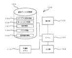
図1は、本発明の実施の形態に係る集積回路設計装置のブロック図である。
図1において、集積回路設計装置100は、中央処理装置(CPU)101、キーボードやマウス等によって構成された入力部102、液晶表示器等によって構成された表示部103、外部記憶装置を構成する磁気ディスク記憶部104、主記憶装置等を構成する半導体メモリ110を備えている。
FIG. 1 is a block diagram of an integrated circuit design apparatus according to an embodiment of the present invention.
In FIG. 1, an integrated
磁気ディスク記憶部104内には、半導体集積回路を構成するデバイス(回路素子)や前記デバイスの集まりであるセル等の回路要素の形状及びその名称を対応付けた情報(レイアウト図形情報)を複数種類記憶したレイアウト図形情報記憶部105、ネットリスト情報(結線情報)を記憶したネットリスト情報記憶部106、複数のデバイスやセルによって構成されるクラスタ等の回路要素の定義や各回路要素の位置関係等の制約を表す情報である制約情報を記憶した制約情報記憶部107、コストとして評価する項目に関する情報(コスト情報)を記憶したコスト情報記憶部108、レイアウトの規則性を評価するために使用する規則性を持つ構造の情報(規則構造情報)を記憶した規則構造情報記憶部109が設けられている。
In the magnetic
前記レイアウト図形情報には、ネットリストを構成するインスタンス(単一又は複数の回路素子(セルやデバイス)によって構成される、1つのまとまった単位の回路要素である。ブロックと称する場合もある。)の形状(枠)の情報が含まれている。
また、前記制約情報は回路要素のレイアウトを行う際に必ず満たす必要のある条件を表す情報(制約)であり、前記制約情報には、複数のデバイスやセルによって構成される回路要素を定義した情報(例えば、クラスタ、ペア、シンメトリ)や、各回路要素の位置関係の制約(例えば、複数の回路要素の水平位置関係の制約や垂直位置関係の制約)を表す情報等のレイアウト時に満たすべき情報が含まれている。
The layout graphic information includes instances constituting a netlist (a single unit of circuit elements composed of a single or a plurality of circuit elements (cells and devices), sometimes referred to as a block). The shape (frame) information is included.
The constraint information is information (constraint) that represents a condition that must be satisfied when the layout of circuit elements is performed, and the constraint information includes information that defines circuit elements composed of a plurality of devices and cells. (For example, a cluster, a pair, a symmetry) and information indicating constraints on the positional relationship of each circuit element (for example, constraints on a horizontal positional relationship and constraints on a vertical positional relationship of a plurality of circuit elements) include.
また、前記コスト情報には、面積や配線長等のコスト評価の対象とする項目の情報が含まれている。
また、前記規則構造情報には、規則性を評価するための基準となる、インスタンスの配置構造の種類が記憶されている。本実施の形態では、後述するようなアレイ、ロウ等の規則的な配置構造を定義した情報が含まれている。
前記レイアウト図形情報、ネットリスト情報、制約情報、コスト情報及び規則構造情報は設計情報を構成している。
The cost information includes information on items to be subjected to cost evaluation such as area and wiring length.
Also, the rule structure information stores the type of instance arrangement structure that serves as a reference for evaluating regularity. In the present embodiment, information defining a regular arrangement structure such as an array and a row as described later is included.
The layout graphic information, net list information, constraint information, cost information, and rule structure information constitute design information.
磁気ディスク記憶部104は、CPU101が実行する集積回路設計用プログラムも記憶しており、CPU101は前記プログラムを実行することにより、後述する処理を行う。
ここで、CPU101は、レイアウトの位相的表現からレイアウトにおける規則構造を抽出しレイアウトの規則構造をレイアウトの最適化指標として評価する評価手段、及び、レイアウトの最適化を行う最適化手段を構成している。前記最適化手段は、レイアウト最適化を行う際に、制約等の必ず満足すべき条件を満たした上で、位相構造の最適化を行い、これを反映して物理構造(例えば、面積や配線長)の最適化を行う。
The magnetic
Here, the
レイアウト図形情報記憶部105は回路要素のレイアウト図形情報を記憶するレイアウト図形情報記憶手段を構成し、ネットリスト情報記憶部106はネットリスト情報を記憶したネットリスト情報記憶手段を構成し、制約情報記憶部107は制約情報記憶手段を構成し、コスト情報記憶部108はコスト情報記憶手段を構成し、規則構造情報記憶部109は規則構造情報記憶手段を構成している。
また、入力部102は入力手段を構成し、表示部103は表示手段を構成し又、磁気ディスク記憶部104及びメモリ110は記憶手段を構成している。
The layout graphic
The
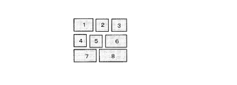
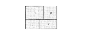
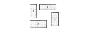
図2〜図7は、本発明の実施の形態において、レイアウトの規則性を評価するために用いる規則構造の例を示す図である。
ここで、レイアウトの規則性とは、個々のインスタンスあるいは複数のインスタンス群が一定の規則でレイアウトされている状態をいう。
例えば、規則性の例として、個々のインスタンスあるいは複数のインスタンス群に対しての、インスタンスのレイアウトの縦及び/又は横方向の整列性(整列性)、インスタンスのレイアウトの回転方向の方向性(方向性)、インスタンスのレイアウトの対称性(X軸対称、Y軸対称、原点対称)(対称性)の3つがある。
2 to 7 are diagrams showing examples of a regular structure used for evaluating the regularity of the layout in the embodiment of the present invention.
Here, the regularity of the layout means a state in which individual instances or a plurality of instances are laid out with a certain rule.
For example, as examples of regularity, the vertical and / or horizontal alignment of the instance layout (alignment) and the rotation direction of the instance layout (direction) with respect to individual instances or a plurality of instances. ) And instance layout symmetry (X axis symmetry, Y axis symmetry, origin symmetry) (symmetry).
LSIの特性上、これらを揃えるあるいは所定配置に指定することが、製造歩留まりの観点から好ましく、特にアナログ要素ではトランジスタのマッチング特性が向上する。また、各回路要素間を配線接続する場合に、配線の容易性等の配線性が向上する。
本実施の形態では、前記3つの規則性の要素(整列性、方向性、対称性)を、レイアウトトポロジとして下記の規則構造に類型化することによって、レイアウトの規則性の評価を可能にしている。
From the viewpoint of manufacturing yield, it is preferable that these are aligned or specified in a predetermined arrangement in terms of the characteristics of the LSI, and in particular, the matching characteristics of the transistor are improved in an analog element. In addition, when the circuit elements are connected by wiring, wiring properties such as wiring ease are improved.
In the present embodiment, the regularity of the layout can be evaluated by classifying the three regularity elements (alignment, directionality, symmetry) into the following regular structure as a layout topology. .
(i)アレイ(Array)
図2に示すように、複数のインスタンスが、マトリクス状にレイアウトされた状態であり、縦及び横が各々同一のピッチ、間隔でレイアウトされている状態である。図2には、9(3×3)個のインスタンス1〜9がアレイ構造にレイアウトされている例を示している。
(I) Array
As shown in FIG. 2, a plurality of instances are laid out in a matrix, and the vertical and horizontal directions are laid out at the same pitch and interval. FIG. 2 shows an example in which 9 (3 × 3)
(ii)ロウ(列並び:Row)
図3に示すように、複数のインスタンスが、縦又は横が同一ピッチ、同一間隔でレイアウトされている状態である。図3には、複数のインスタンス1〜8が、縦方向が同一ピッチ、同一間隔でレイアウトされており、縦方向3段のロウ構造のレイアウト例を示している。
(Ii) Row (row arrangement: Row)
As shown in FIG. 3, a plurality of instances are laid out at the same pitch and the same interval in the vertical or horizontal direction. In FIG. 3, a plurality of
(iii)スライス(Slice)
図4に示すように、任意のインスタンスを直線によって2分割できるようにレイアウトされている状態である。図4には、インスタンス1、2とインスタンス3、4とを横線によって2分割できるように配置されたスライス構造の例を示している。
(Iii) Slice
As shown in FIG. 4, the layout is such that an arbitrary instance can be divided into two by a straight line. FIG. 4 shows an example of a slice structure arranged so that
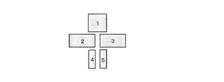
(iv)ルーム(Room)
図5に示すように、破線で示すように所定領域を複数の矩形領域(ルーム)に分割し、前記各矩形領域に空きが生じないように、前記各矩形領域に1つのインスタンスを配置した状態であり、スライスを包含する概念である。図5には、所定領域を5つの矩形領域に分割し、各矩形領域内に1つのインスタンス1〜5を配置したルーム構造の例を示している。
(Iv) Room (Room)
As shown in FIG. 5, a state in which a predetermined area is divided into a plurality of rectangular areas (rooms) as indicated by broken lines, and one instance is arranged in each rectangular area so that there is no space in each rectangular area It is a concept that encompasses slices. FIG. 5 shows an example of a room structure in which a predetermined area is divided into five rectangular areas and one
(v)オブジェクト(Object)
図6に示すように、任意のコンパクションを行った後のレイアウト状態であり、各インスタンス1〜4が任意の座標を持つ状態である。
ここで、前記5種類のレイアウトトポロジ(i)〜(v)は、アレイ、ロウ、スライス、ルーム、オブジェクトの順で、規則性の観点からの優先度が低くなる(アレイ>ロウ>スライス>ルーム>オブジェクト)ように設定している。前記優先度に対応する評価値を予め設定しておくことにより、規則性の評価を数値化することができる。
尚、前記規則構造以外にも、図7に示す規則構造「シンメトリ(Symmetry)」のように、複数のインスタンス1〜5が線対称になるように配置した状態も含めるようにしてもよい。
(V) Object (Object)
As shown in FIG. 6, it is a layout state after performing arbitrary compaction, and each
Here, the five types of layout topologies (i) to (v) have a lower priority from the viewpoint of regularity in the order of array, row, slice, room, and object (array>row>slice> room). > Object). By setting an evaluation value corresponding to the priority in advance, the regularity evaluation can be quantified.
In addition to the regular structure, a state in which a plurality of
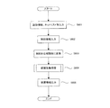
図8及び図9は、本発明の実施の形態に係る集積回路設計装置100の動作を示すフローチャートである。
図10は、物理的な構造評価値の1つである局所詰め込み値(局所への詰め込み具合の指標となる値)を説明するための図である。図10において、局所詰め込み値は、局所配置の詰め込み率を向上させるためのコストである。局所詰め込み値は、「ブロック1〜8の面積の総和/ブロック1〜8を囲む最小矩形1001の面積」である。局所詰め込み値は、値が大きいほど空き領域が多いことを示しており、局所詰め込み値が大きいほど、コストが高くなる。
8 and 9 are flowcharts showing the operation of the integrated
FIG. 10 is a diagram for explaining a local stuffing value (a value serving as an index of the degree of stuffing into the local area), which is one of the physical structure evaluation values. In FIG. 10, the local stuffing value is a cost for improving the stuffing rate of local arrangement. The local stuffing value is “total area of
図11は、物理的な構造評価値の1つである局所均一値(ロウにおける均一性の指標となる値)を説明するための図である。
ロウは複数のブロックがマトリクス的に配置された構造であり、水平方向のロウの場合は、各段のブロックの高さは同じであるが、ブロックの幅は異なる。各段でのブロックの幅の最大幅と最小幅の差を、全ての段で加算したものを評価して数値化し(この値を局所均一値という。)、前記局所均一値が小さい程、均一なロウであると判断する。縦方向のロウの場合も、前記同様にして局所均一値を求めて均一性を評価する。
FIG. 11 is a diagram for explaining a local uniform value (a value serving as an index of uniformity in a row) that is one of physical structure evaluation values.
A row has a structure in which a plurality of blocks are arranged in a matrix. In the case of a row in the horizontal direction, the height of the blocks in each stage is the same, but the width of the blocks is different. The difference between the maximum width and the minimum width of the block width at each stage is evaluated and digitized by adding all the stages (this value is referred to as a local uniform value). The smaller the local uniform value, the more uniform Judged to be a low law. Even in the case of a row in the vertical direction, the uniformity is evaluated by obtaining a local uniform value in the same manner as described above.
例えば図11において、局所均一値は、水平方向ロウのブロックの幅を均一にするためのコストであり、局所均一値は、「(ブロック1〜4の最大幅−最小幅)+(ブロック5〜8の最大幅−最小幅)」である。
また、図12〜図14は、本発明の実施の形態に係る集積回路設計装置100において、最適化処理の例を示す図である。
For example, in FIG. 11, the local uniform value is a cost for making the width of the horizontal row block uniform, and the local uniform value is “(maximum width of
12 to 14 are diagrams showing examples of optimization processing in the integrated
以下、図1〜図14を用いて、本発明の実施の形態に係る集積回路設計装置及び集積回路設計用プログラムについて詳細に説明する。
先ず、ユーザ(例えば、半導体集積回路の設計者)が入力部102を操作して設計処理開始の指示を入力すると、CPU101は、磁気ディスク記憶部104に記憶しておいた前記集積回路設計用プログラム及び設計情報をメモリ110に読み込み、前記集積回路設計用プログラムを実行することにより、入力部102からの入力に応じた処理を行うことができる状態になる。
Hereinafter, an integrated circuit design device and an integrated circuit design program according to an embodiment of the present invention will be described in detail with reference to FIGS.
First, when a user (for example, a semiconductor integrated circuit designer) operates the
即ち、CPU101は、レイアウト図形情報記憶部105からレイアウト図形情報を、ネットリスト情報記憶部106からネットリスト情報を、コスト情報記憶部108からコスト情報を、規則構造情報記憶部109から規則構造情報を読み込んで、メモリ110に入力する(ステップS801)。ここで、ネットリストは階層構造でもよい。
また、CPU101は、制約情報記憶部107から制約情報を読み込んでメモリ110に入力する(ステップS802)。
That is, the
Further, the
本実施の形態では、シーケンスペア法を用いて、規則性構造の評価や配置改善を行うようにしているため、CPU101は、前記制約情報の制約を位相関係に変換した後(ステップS803)、規則性情報を参照すると共に前記レイアウト図形情報、ネットリスト情報及び制約情報を用いて、前記制約を満足するように、レイアウトの最適化を行うために配置改善処理を行う(ステップS804)。
In the present embodiment, since the regularity structure is evaluated and the arrangement is improved by using the sequence pair method, the
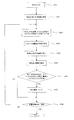
処理ステップS804の配置改善処理では図9に示す処理が行われる。即ち、CPU101は先ず、処理ステップS802で入力した制約を満たす初期解(レイアウトモデル)Xを作成する(図9のステップS901)。前記初期解Xは前記制約を満たす任意の解である。
次にCPU101は、処理ステップS901で得られた解Xに対してトポロジ的な変更やトポロジを保持してのブロック交換を行うことによって、新しい解X’(レイアウトモデル)の作成を行う(ステップS902)。
In the arrangement improving process in process step S804, the process shown in FIG. 9 is performed. That is, the
Next, the
ここで、「トポロジ的」とは、任意のレイアウト対の関係を「上下関係」、もしくは「左右関係」のどちらかの位置関係(位相関係)によって表現することを意味しており、レイアウト全体のブロック位置関係を物理的に表現するのではなく、トポロジによって表現することである。 Here, “topological” means that the relationship between any layout pair is expressed by the positional relationship (topological relationship) of either “vertical relationship” or “left-right relationship”. Instead of physically expressing the block position relationship, it is expressed by topology.
この表現方法には、たとえばBSG法(Bounded-Sliceline Grid)、シーケンスペア法(Sequence-Pair)、オーツリー法(O-Tree)、 ビーツリー法(B*-Tree)、TCG−S法等の既知の方法があるが、本実施の形態では、シーケンスペア法でのアルゴリズムを例に説明する。
次にCPU101は、前記解X’に関して、前記トポロジ的な表現からレイアウトの規則性を抽出することにより、トポロジ的な構造評価値を算出する(ステップS903)。
This representation method includes known methods such as the BSG method (Bounded-Sliceline Grid), sequence pair method (Sequence-Pair), O-tree method (O-Tree), Bee tree method (B * -Tree), TCG-S method, etc. There is a method, but in this embodiment, an algorithm using the sequence pair method will be described as an example.
Next, the
以下に一例として、シーペンスペア法を用いて、アレイ、ロウ及びシンメトリを抽出する手法を示すが、シーケンスペア法では、ブロックレイアウトにおいて、左上方向に、他のブロックに接触せずに取り出す順番を考える場合、これを「左上列」と呼ぶ。同様に、左下方向に取り出す順を「左下列」と呼ぶ。この左上列と左下列の対がシーケンスペアに対応する。また、左上列を1、2、3、・・・と連続昇順の番号でブロック名を置き換えたときに対応する左下列がシングルシーケンス(Single-Sequence)に対応する。 As an example, the method of extracting arrays, rows, and symmetry using the Seapen Spare method is shown below, but in the sequence pair method, when considering the order of extraction without touching other blocks in the upper left direction in the block layout This is called “upper left column”. Similarly, the order of taking out in the lower left direction is referred to as a “lower left column”. The pair of the upper left column and the lower left column corresponds to a sequence pair. The upper left column corresponds to a single sequence (Single-Sequence) when the block name is replaced with 1, 2, 3,...
先ず、アレイ及びロウレイアウトトポロジ構造(位相構造)の抽出を行う場合には、あるブロックレイアウト、もしくは部分レイアウトに着目する。そのレイアウトのシングルシーケンス表記に従い、要素番号が、連続、かつ昇順(以下、連続昇順)になっている場合は、そのレイアウトは水平方向の1列のレイアウトトポロジに対応していると判断できる(以下、水平1列レイアウト)。また、要素番号が、連続、かつ降順(以下、連続降順)になっている場合は、そのレイアウトは垂直方向の1列のレイアウトトポロジに対応していると判断できる(以下、垂直1列レイアウト)。
First, when extracting an array and row layout topology structure (phase structure), attention is paid to a certain block layout or partial layout. According to the single sequence notation of the layout, when the element numbers are continuous and in ascending order (hereinafter, continuous ascending order), it can be determined that the layout corresponds to the layout topology of one column in the horizontal direction (hereinafter, the following)
さらに、これらの水平1列レイアウトをそれぞれ1ブロックに置き換える。そのレイアウトにおいて、上記と同様の手順で、連続降順となる列を抽出したとき、そのレイアウトは、水平列を積み重ねた多段ロウのレイアウトトポロジに対応していると判断できる。
同様に、垂直1列レイアウトをそれぞれ1ブロックに置き換え、そのレイアウトにおいて、連続昇順となる列を抽出したとき、そのレイアウト、垂直列を複数段積み重ねた多段ロウのレイアウトトポロジに対応していると判断できる。
Further, each of these horizontal one-row layouts is replaced with one block. In the layout, when columns in descending order are extracted in the same procedure as described above, it can be determined that the layout corresponds to the layout topology of a multistage row in which horizontal columns are stacked.
Similarly, when each vertical one-column layout is replaced with one block, and columns in the ascending order are extracted from the layout, it is determined that the layout and the vertical column correspond to the multi-row layout topology in which a plurality of stages are stacked. it can.
以上のすべての手順は、ブロック数に応じた数の処理を行うことにより実行可能である。
特殊な場合として、積み重ねられた水平1列レイアウトがすべて同じブロック数をもつとき、アレイレイアウトトポロジに対応していると判断できる。同様に、積み重ねられた垂直1列レイアウトがすべて同じブロック数をもつとき、アレイレイアウトトポロジに対応していると判断できる。
All the above procedures can be executed by performing a number of processes corresponding to the number of blocks.
As a special case, when all the stacked horizontal single-line layouts have the same number of blocks, it can be determined that the layout corresponds to the array layout topology. Similarly, when the stacked vertical one-column layouts all have the same number of blocks, it can be determined that the array layout topology is supported.
また、シンメトリトポロジの抽出を行う場合には、あるブロックレイアウト、もしくは部分レイアウトに着目し、そのレイアウトから抽出したシングルシーケンスと、そのレイアウトを水平方向にY軸反転したレイアウトから抽出したシングルシーケンスが同一であるとき、このレイアウトは、完全水平対称トポロジを持つと判断できる。同様に、そのブロックレイアウトから抽出したシングルシーケンスと、そのレイアウトを垂直方向にX軸反転したレイアウトから抽出したシングルシーケンスが同一であるとき、レイアウトは、完全垂直対称トポロジを持つと判断できる。 When extracting a symmetry topology, paying attention to a certain block layout or partial layout, the single sequence extracted from the layout and the single sequence extracted from the layout obtained by inverting the layout in the Y axis in the horizontal direction are the same. Then it can be determined that this layout has a perfectly horizontal symmetry topology. Similarly, when the single sequence extracted from the block layout and the single sequence extracted from the layout obtained by inverting the layout in the X direction in the vertical direction are the same, it can be determined that the layout has a completely vertical symmetric topology.
次に、CPU101は、規則性の評価を行う場合、例えば次のようにして行う。
先ず、CPU101は、下記のトポロジカル構造評価値及び物理的な構造評価値をコンパクション前(具体的な座標値が確定する前)に算出する。
(1)トポロジ的な構造評価値の算出
(a)アレイトポロジ構造を構成しているブロック数と、各トポロジの行数と列数の比(アスペクト)とから、アスペクトが1に近いアレイの数に比例して大きくなるように算出した値
Next, when evaluating regularity, the
First, the
(1) Calculation of topological structure evaluation value (a) Number of arrays whose aspect is close to 1 from the number of blocks constituting the array topology structure and the ratio (aspect) of the number of rows and columns of each topology Calculated to increase in proportion to
(b)ロウトポロジを構成しているブロック数とアスペクトとから、アスペクトが1に近いロウの数に比例して大きくなるように算出した値
(c)自己シンメトリ(自分自身に対称)以外の対称トポロジを構成しているブロック数に比例するように算出した値
((a)+(b)+(c))の値をトポロジ的な構造評価値とする。
(B) A value calculated from the number of blocks constituting the row topology and the aspect so that the aspect increases in proportion to the number of rows close to 1. (c) A symmetric topology other than self-symmetry (symmetric to itself). The value of ((a) + (b) + (c)) calculated so as to be proportional to the number of blocks constituting is used as the topological structure evaluation value.
(2)物理的な構造評価値の算出(ステップS904)
(d)局所詰め込み値の算出
前記(1)のブロックに対して、「各ブロックの面積の総和/各ブロックを囲む最小矩形の面積」を局所詰め込み値として求める。これにより詰め込み具合を算出する(値が大きいほど空き領域が多く、コストが高い)。
(2) Calculation of physical structure evaluation value (step S904)
(D) Calculation of Local Packing Value For the block (1), “total area of each block / minimum rectangular area surrounding each block” is obtained as a local packing value. Thus, the degree of packing is calculated (the larger the value, the more free space and the higher the cost).
(e)局所均一値の算出
各段でのブロックの幅の最大幅と最小幅の差を、全ての段で加算したものを評価して数値化することにより、局所均一値を算出する。
ここでは、前記(1)の複数列に対して、各列のブロックの最大、最小幅の差を総計したものが大きいほど、均一でなく、コストが高くなる。
((d)+(e))の値を物理的な構造評価値とする。
(E) Calculation of local uniform value The local uniform value is calculated by evaluating and digitizing the difference between the maximum width and the minimum width of the block width in each stage and adding it in all stages.
Here, the larger the sum of the differences between the maximum and minimum widths of the blocks in each column with respect to the plurality of columns of (1), the more uniform and the higher the cost.
The value of ((d) + (e)) is set as a physical structure evaluation value.
次に、CPU101は、コストの要素である配線長及び面積を算出する(ステップS905)。
次に、CPU101は、処理ステップS902で作成した解X’が制約を満たすか否かを判断し、解Xが制約を満足する場合には解X’と解Xとのコスト比較を行い、より適した方の解を選択する(ステップS906)。
Next, the
Next, the
ここで使用するコスト及び制約は次の通りである。
(A)制約
制約は必ず守るべき条件であり、例えばブロックの隣接制約や、具体的なブロック名を指定したシンメトリ制約、あるいは寄生成分(抵抗、容量)などの影響を考慮した制約などがあり、これらは、具体的な座標値を求めるコンパクションの前後で、制約をチェックし、許容解か否かを判断する。
The costs and constraints used here are as follows.
(A) Constraints Constraints are conditions that must be observed, such as block adjacency constraints, symmetry constraints that specify specific block names, or constraints that take into account the effects of parasitic components (resistance, capacitance), etc. These check the constraints before and after compaction for obtaining specific coordinate values, and determine whether or not they are acceptable solutions.
(B)コンパクション前のトポロジカル構造評価値、物理的な構造評価値のコスト
このコストは、処理ステップS903、S904で算出された構造評価値に基づくコストであり、これらは前記(A)の制約で明示的に指定されたブロック以外にも適応される。即ち、このコストは、外部から制約として指定されていない場合でも、自動的に算出される。
(C)コンパクション後の面積、配線長などのコスト
このコストは、一般的なブロックの実座標値が確定した後に評価されるコストであり、面積最小、配線長(総配線、特定配線を含む)最小を目標とする。
(B) Topological structure evaluation value before compaction, cost of physical structure evaluation value This cost is a cost based on the structure evaluation value calculated in processing steps S903 and S904, and these are the constraints of (A). Applies to blocks other than explicitly specified blocks. That is, this cost is automatically calculated even if it is not designated as a constraint from the outside.
(C) Cost after area of compaction, wiring length, etc. This cost is evaluated after the actual coordinate value of a general block is determined, and the minimum area, wiring length (including total wiring and specific wiring) Target the minimum.
CPU101は、前記(A)の制約を守りつつ、前記(B)、(C)のコストを最適化(例えば最小化)するようにして、レイアウトを最適化する。
即ち、CPU101は、処理ステップS906において、新たな解X’が制約を満たし、且つ、新たな解X’と解Xのコスト比較を行うことによって解X’のコストが解Xのコストよりも小さいか否かを判断する。
The
That is, the
CPU101は、新たな解X’が制約を満たし、且つ、解Xよりもコストが小さいと判断すると、解を解Xから解X’に更新した後(ステップS907)、配置改善の終了条件が満たされたか否かを判断する(ステップS908)。
前記配置改善の終了条件としては、例えば、最適化手法がSA(Simulated Anneiling)法の場合には温度が所定温度(例えば、100度から0度まで)、遺伝的アルゴリズム(GA)法の場合には世代数等である。
When the
As an end condition for the layout improvement, for example, when the optimization method is the SA (Simulated Anneiling) method, the temperature is a predetermined temperature (for example, from 100 degrees to 0 degrees), and when the genetic algorithm (GA) method is used. Is the number of generations.
一方、CPU101は、処理ステップS906において、新たな解X’が制約を満たさないと判断した場合や、解X’が解Xよりもコストが小さくないと判断した場合、直ちに処理ステップS908に移行する。
CPU101は、処理ステップS908において、配置改善の終了条件が満たされていないと判断した場合には処理ステップS902に戻って前記処理を繰り返し、配置改善の終了条件が満たされたと判断した場合には、得られた集積回路のレイアウトのデータを磁気ディスク記憶部104に記憶し、表示部103あるいは外部の装置に出力する(ステップS805)。
On the other hand, if the
If the
このようにして、前記項目(A)、(B)、(C)の複合的な制約、コストを最適化アルゴリズムの中で調整することで、従来の集積回路設計装置において用いていた項目(A)、(C)に加えて、(B)の規則性を考慮したレイアウト結果を得ることができる。
前記の如くして行った最適化処理の一例を図12〜図14に沿って説明する。
In this way, the items (A) used in the conventional integrated circuit design apparatus are adjusted by adjusting the complex constraints and costs of the items (A), (B), and (C) in the optimization algorithm. In addition to (C), a layout result considering the regularity of (B) can be obtained.
An example of the optimization process performed as described above will be described with reference to FIGS.
図12は、複数のブロックa〜dの配置を行った最初の状態(初期状態)を示す図である。図12の初期状態は、複数のブロックa〜dが配置された最初の状態であり、アレイ構造の個数(アレイ数)は0であり又、物理的な総配線長は2.5である。双矢印線は物理的な配線であり、これらの配線の合計が総配線長である。本例における最適化処理の目標は、アレイのコストの最小化(即ち、アレイ数の最大化)及び物理的な総配線長であるコストの最小化である。 FIG. 12 is a diagram illustrating an initial state (initial state) in which a plurality of blocks a to d are arranged. The initial state of FIG. 12 is an initial state in which a plurality of blocks a to d are arranged, the number of array structures (number of arrays) is 0, and the total physical wiring length is 2.5. The double arrow line is a physical wiring, and the total of these wirings is the total wiring length. The goals of the optimization process in this example are to minimize the cost of the array (ie, to maximize the number of arrays) and to minimize the cost, which is the total physical wiring length.
図13は、図12の状態から、トポロジ最適化によってアレイ構造が形成された状態を示している。ここで、アレイ数は1であり、総配線長は4である。但し、総配線長は必ずしも最適化されたものではない。
図14は、図13の状態から変化して、トポロジのコストが劣化しないという制約の下で、物理的なコストを最適化した状態を示している。ここで、アレイ数は1、総配線長は2が得られており、アレイ数の最大化及び物理的総配線長のコストの最小化が実現されている。
FIG. 13 shows a state in which an array structure is formed by topology optimization from the state of FIG. Here, the number of arrays is 1, and the total wiring length is 4. However, the total wiring length is not necessarily optimized.
FIG. 14 shows a state in which the physical cost is optimized under the restriction that the cost of the topology does not deteriorate from the state of FIG. Here, the number of arrays is 1 and the total wiring length is 2, and the maximization of the number of arrays and the minimization of the cost of the physical total wiring length are realized.
このようにして、前記(A)、(B)、(C)の複合的な制約、コストを最適化アルゴリズムの中で調整することで、前記(B)の規則性を考慮したレイアウト結果を得ることができる。即ち、コスト計算に際して、規則性の観点からコストを補正するように処理することにより、高い規則性を有するレイアウトの場合、よりコストを小さくすることができる。 In this way, by adjusting the complex constraints and costs of (A), (B), and (C) in the optimization algorithm, a layout result in consideration of the regularity of (B) is obtained. be able to. That is, in the cost calculation, by processing so as to correct the cost from the viewpoint of regularity, the cost can be further reduced in the case of a layout having high regularity.
以上述べたように、本発明の実施の形態に係る集積回路設計装置は、レイアウトの位相的表現からレイアウトにおける規則構造を抽出し、前記抽出したレイアウトの規則構造をレイアウトの最適化指標として評価し、レイアウト最適化を行う際に、位相構造と物理構造(面積や配線長等のコスト)の最適化を行うようにしている。
即ち、CPU101は、磁気ディスク記憶部104の規則構造情報記憶部107に記憶された規則構造情報を参照すると共にレイアウト図形情報、ネットリスト情報及び制約情報を用いてレイアウトにおける規則構造を抽出し、前記規則構造を評価し、前記評価を考慮して、レイアウト図形情報、ネットリスト情報等の設計情報を用いて最適化した集積回路のレイアウトを得るようにしている。
As described above, the integrated circuit design device according to the embodiment of the present invention extracts a rule structure in a layout from a topological expression of the layout, and evaluates the extracted rule structure of the layout as a layout optimization index. When the layout is optimized, the phase structure and the physical structure (costs such as area and wiring length) are optimized.
That is, the
したがって、より規則的に並んだレイアウトを得ることによって、良好な回路特性を持ち又、総配線長の短い良好な配線性を持つレイアウト結果を得ることが可能になる。
また、レイアウト最適化処理において、新たに規則性の指標を組み込みことで、明示的なアライメントなどの制約がなくとも、レイアウト結果が自動的に、アレイ、ロウ、スライス等の規則構造を考慮するようになり、これに従来の面積や配線長のコスト、及び、ペア性、シンメトリ性などの付加的な制約を合わせて自動レイアウトを行うことで、よりアナログ設計者の望む、規則的な、いわばきれいなレイアウトを得ることが可能になる。
Therefore, by obtaining a more regularly arranged layout, it is possible to obtain a layout result having good circuit characteristics and good wiring properties with a short total wiring length.
Also, by incorporating a new regularity index in the layout optimization process, the layout result will automatically take into account the regular structure such as array, row, slice, etc., even if there is no explicit alignment restriction. By combining this with additional constraints such as the cost of conventional area and wiring length, and pairing, symmetry, etc., automatic layout is performed, so the analog designer wants more regular, so-called cleanliness. A layout can be obtained.
また、外部から明示的な制約を指定せずに、内部で規則性を考慮することで、最小限の付加的な制約を用いて、自動レイアウト結果が規則的なレイアウト結果となる。その結果として、歩留まりの向上や良好なマッチング特性を得ることが可能になり、さらには 短く単純な配線によって各回路要素を接続できるため、各回路要素を適切な配線によって容易に接続できる等の配線性が向上し、レイアウト設計効率が向上するという効果を奏する。 Further, by considering regularity internally without specifying an explicit constraint from the outside, an automatic layout result becomes a regular layout result using a minimum additional constraint. As a result, it becomes possible to improve the yield and obtain good matching characteristics, and furthermore, since each circuit element can be connected by short and simple wiring, each circuit element can be easily connected by appropriate wiring. This improves the performance and improves the layout design efficiency.
アナログ半導体集積回路のみならずデジタル半導体集積回路の設計にも良好に適用可能であるが、特にアナログ半導体集積回路において優れたレイアウト結果を得ることができる。
また、本発明の実施の形態に係る集積回路設計用プログラムをコンピュータに実行させることにより、コンピュータを用いて前記集積回路設計装置を構築することが可能になる。
Although the present invention can be satisfactorily applied to the design of not only analog semiconductor integrated circuits but also digital semiconductor integrated circuits, excellent layout results can be obtained particularly in analog semiconductor integrated circuits.
Further, by causing a computer to execute the integrated circuit design program according to the embodiment of the present invention, the integrated circuit design apparatus can be constructed using the computer.
尚、トポロジ的な規則構造の評価を行って評価値を算出する場合、アレイ、ロウ、スライス、ルーム、オブジェクトの中の少なくとも1つを評価して評価値を算出するように構成してもよい。
また、物理的な規則構造の評価を行って評価値を算出する場合、局所詰め込み値及び局所均一値の中の少なくとも1つを評価して評価値を算出するように構成してもよい。
When the evaluation value is calculated by evaluating the topological regular structure, the evaluation value may be calculated by evaluating at least one of the array, the row, the slice, the room, and the object. .
Further, when the evaluation value is calculated by evaluating the physical regular structure, the evaluation value may be calculated by evaluating at least one of the local stuffing value and the local uniform value.
アナログ半導体集積回路やデジタル半導体集積回路の設計を行う集積回路設計装置に適用可能である。また、コンピュータをアナログ半導体集積回路やデジタル半導体集積回路の設計を行う集積回路設計装置として機能させるプログラムに適用可能である。 The present invention can be applied to an integrated circuit design apparatus that designs analog semiconductor integrated circuits and digital semiconductor integrated circuits. Further, the present invention can be applied to a program that causes a computer to function as an integrated circuit design apparatus that designs analog semiconductor integrated circuits and digital semiconductor integrated circuits.
100・・・集積回路設計装置
101・・・評価手段及びレイアウトの最適化を行う最適化手段を構成するCPU
102・・・入力手段を構成する入力部
103・・・表示手段を構成する表示部
104・・・記憶手段を構成する磁気ディスク記憶部
105・・・レイアウト図形情報記憶手段を構成するレイアウト図形情報記憶部
106・・・ネットリスト情報記憶手段を構成するネットリスト情報記憶部
107・・・制約情報記憶手段を構成する制約情報記憶部
108・・・コスト情報記憶手段を構成するコスト情報記憶部
109・・・規則構造情報記憶手段を構成する規則構造情報記憶部
110・・・記憶手段を構成する半導体メモリ
1001・・・最小矩形
DESCRIPTION OF
DESCRIPTION OF
Claims (8)
レイアウトにおける規則構造を抽出して前記レイアウトの規則性の評価を行う評価手段と、
前記設計情報に基づいて集積回路のレイアウトを最適化する最適化手段とを備え、
前記設計情報には、前記規則構造を表す規則構造情報、レイアウト図形情報、ネットリスト情報、制約情報及びコスト情報が含まれ、
前記評価手段は、前記規則構造情報を参照すると共に前記レイアウト図形情報、ネットリスト情報及び制約情報を用いて、前記規則構造を抽出して前記規則性の評価を行い、
前記最適化手段は、前記制約情報に含まれる制約を満足させると共に前記評価手段による規則性の評価を考慮して、前記レイアウト図形情報、ネットリスト情報及びコスト情報を用いて、前記集積回路のレイアウトを最適化することを特徴とする集積回路設計装置。 Storage means for storing design information necessary for designing an integrated circuit;
An evaluation means for extracting a rule structure in the layout and evaluating the regularity of the layout;
Optimizing means for optimizing the layout of the integrated circuit based on the design information,
The design information includes rule structure information representing the rule structure, layout graphic information, net list information, constraint information, and cost information.
The evaluation means refers to the rule structure information and uses the layout graphic information, netlist information and constraint information to extract the rule structure and evaluate the regularity.
The optimization means satisfies the constraints included in the constraint information and takes into account the regularity evaluation by the evaluation means, and uses the layout graphic information, netlist information, and cost information to layout the integrated circuit. An integrated circuit design apparatus characterized by optimizing
前記評価手段は、トポロジ的な規則構造に基づく規則性の評価を行う場合、前記規則構造の中の少なくとも1つの規則構造に基づいて評価を行うことを特徴とする請求項2記載の集積回路設計装置。 Array, waxes, include at least one among the slice become the said regular structure,
3. The integrated circuit design according to claim 2 , wherein when evaluating the regularity based on a topological regular structure, the evaluation means performs the evaluation based on at least one regular structure in the regular structure. apparatus.
レイアウトにおける規則構造を抽出して前記レイアウトの規則性の評価を行う評価手段と、
記憶手段に記憶された集積回路の設計に必要な設計情報に基づいて集積回路のレイアウトを最適化する最適化手段とを備え、
前記設計情報には、前記規則構造を表す規則構造情報、レイアウト図形情報、ネットリスト情報、制約情報及びコスト情報が含まれ、
前記評価手段が、前記規則構造情報を参照すると共に前記レイアウト図形情報、ネットリスト情報及び制約情報を用いて、前記規則構造を抽出して前記規則性の評価を行い、
前記最適化手段が、前記制約情報に含まれる制約を満足させると共に前記評価手段による規則性の評価を考慮して、前記レイアウト図形情報、ネットリスト情報及びコスト情報を用いて、前記集積回路のレイアウトを最適化するように機能させることを特徴とする集積回路設計用プログラム。 Computer
An evaluation means for extracting a rule structure in the layout and evaluating the regularity of the layout;
Optimization means for optimizing the layout of the integrated circuit based on design information necessary for designing the integrated circuit stored in the storage means,
The design information includes rule structure information representing the rule structure, layout graphic information, net list information, constraint information, and cost information.
The evaluation means refers to the rule structure information and uses the layout graphic information, netlist information and constraint information to extract the rule structure and evaluate the regularity.
The optimization means satisfies the constraints included in the constraint information and considers the evaluation of the regularity by the evaluation means, and uses the layout graphic information, netlist information, and cost information to layout the integrated circuit. A program for designing an integrated circuit , which functions to optimize the function .
前記評価手段がトポロジ的な規則構造に基づく規則性の評価を行う場合、前記規則構造の中の少なくとも1つの規則構造に基づいて評価を行うようにコンピュータを機能させることを特徴とする請求項6記載の集積回路設計用プログラム。 Array, waxes, include at least one among the slice become the said regular structure,
If the evaluation means for evaluating the regularity based on topological regular structure, according to claim 6, characterized in that causes a computer to function so as to perform the evaluation based on at least one ordered structure in the ordered structure The integrated circuit design program described.
Priority Applications (2)
| Application Number | Priority Date | Filing Date | Title |
|---|---|---|---|
| JP2006324227A JP4771925B2 (en) | 2006-11-30 | 2006-11-30 | Integrated circuit design apparatus and integrated circuit design program |
| US11/703,700 US7698663B2 (en) | 2006-11-30 | 2007-02-08 | Apparatus, method and program for designing integrated circuit |
Applications Claiming Priority (1)
| Application Number | Priority Date | Filing Date | Title |
|---|---|---|---|
| JP2006324227A JP4771925B2 (en) | 2006-11-30 | 2006-11-30 | Integrated circuit design apparatus and integrated circuit design program |
Publications (2)
| Publication Number | Publication Date |
|---|---|
| JP2008140011A JP2008140011A (en) | 2008-06-19 |
| JP4771925B2 true JP4771925B2 (en) | 2011-09-14 |
Family
ID=39477355
Family Applications (1)
| Application Number | Title | Priority Date | Filing Date |
|---|---|---|---|
| JP2006324227A Expired - Fee Related JP4771925B2 (en) | 2006-11-30 | 2006-11-30 | Integrated circuit design apparatus and integrated circuit design program |
Country Status (2)
| Country | Link |
|---|---|
| US (1) | US7698663B2 (en) |
| JP (1) | JP4771925B2 (en) |
Families Citing this family (5)
| Publication number | Priority date | Publication date | Assignee | Title |
|---|---|---|---|---|
| TW200837588A (en) * | 2007-03-07 | 2008-09-16 | Advanced Analog Technology Inc | Aid design system for analog integrated circuit and the method thereof |
| US9003351B1 (en) | 2014-01-08 | 2015-04-07 | Freescale Semiconductor, Inc. | System and method for reducing power consumption of integrated circuit |
| CN108920746B (en) * | 2018-05-17 | 2022-07-26 | 佛山市顺德区中山大学研究院 | A pre-compression method and system for integrated circuit layout planning |
| US11824009B2 (en) | 2018-12-10 | 2023-11-21 | Preferred Networks, Inc. | Semiconductor device and data transferring method for semiconductor device |
| US20250291990A1 (en) * | 2024-03-13 | 2025-09-18 | Novatek Microelectronics Corp. | Method for learning-based auto placement of analog circuit |
Family Cites Families (9)
| Publication number | Priority date | Publication date | Assignee | Title |
|---|---|---|---|---|
| JP3556260B2 (en) * | 1993-02-12 | 2004-08-18 | 株式会社東芝 | LSI element arrangement method and apparatus |
| JPH0773217A (en) * | 1993-09-03 | 1995-03-17 | Mitsubishi Electric Corp | Automatic element placement device |
| US6557159B1 (en) * | 2000-05-24 | 2003-04-29 | International Business Machines Corporation | Method for preserving regularity during logic synthesis |
| US6598215B2 (en) * | 2001-03-30 | 2003-07-22 | Intel Corporation | Datapath design methodology and routing apparatus |
| JP4597441B2 (en) * | 2001-09-14 | 2010-12-15 | ルネサスエレクトロニクス株式会社 | Analog cell layout design equipment |
| JP2004234450A (en) | 2003-01-31 | 2004-08-19 | Jedat Inc | Semiconductor integrated circuit layout change processing device |
| JP2005062943A (en) | 2003-08-12 | 2005-03-10 | Jedat Innovation:Kk | Integrated circuit design equipment |
| JP2005267291A (en) * | 2004-03-19 | 2005-09-29 | Shigehisa Nakatake | Integrated circuit design equipment |
| JP2006309748A (en) * | 2005-03-30 | 2006-11-09 | Tokyo Univ Of Agriculture & Technology | Rectangular element arrangement method, rectangular element arrangement apparatus, and rectangular element arrangement program |
-
2006
- 2006-11-30 JP JP2006324227A patent/JP4771925B2/en not_active Expired - Fee Related
-
2007
- 2007-02-08 US US11/703,700 patent/US7698663B2/en not_active Expired - Fee Related
Also Published As
| Publication number | Publication date |
|---|---|
| JP2008140011A (en) | 2008-06-19 |
| US7698663B2 (en) | 2010-04-13 |
| US20080134105A1 (en) | 2008-06-05 |
Similar Documents
| Publication | Publication Date | Title |
|---|---|---|
| US11544437B2 (en) | System for designing integrated circuit layout and method of making the integrated circuit layout | |
| CN115315703A (en) | Generating an integrated circuit layout using a neural network | |
| US20210097224A1 (en) | Method and system for generating layout design of integrated circuit | |
| US8631374B2 (en) | Cell architecture for increasing transistor size | |
| US8423941B2 (en) | Structural migration of integrated circuit layout | |
| US20100025859A1 (en) | Method for designing semiconductor device, program therefor, and semiconductor device | |
| US8924913B1 (en) | Schematic display of connectivity in an integrated circuit design | |
| CN119514474B (en) | Automatic design arrangement and path planning method and system for double-panel and multi-layer board printed circuits | |
| CN114764554B (en) | Waveguide bus and methods and systems for automatically generating waveguide bus layouts | |
| TW201923823A (en) | Integrated circuit and its design method and design system thereof | |
| CN120106007B (en) | Clock tree synthesis method and system based on clustering | |
| US7698663B2 (en) | Apparatus, method and program for designing integrated circuit | |
| CN118839664A (en) | Method, device, equipment and storage medium for adding via holes of integrated circuit layout | |
| CN109074412B (en) | Interactive routing of connections in circuits using auto-soldering and auto-cloning | |
| US20140245251A1 (en) | Design Optimization for Circuit Migration | |
| Sadeghi et al. | Automatic and simultaneous floorplanning and placement in field-programmable gate arrays with dynamic partial reconfiguration based on genetic algorithm | |
| Lee et al. | Contango: Integrated optimization of SoC clock networks | |
| US8555232B2 (en) | Wire routing using virtual landing pads | |
| TWI898088B (en) | Poly-bit cells and methods for forming the same | |
| Wang et al. | Effective regularity extraction and placement techniques for datapath‐intensive circuits | |
| JP4668974B2 (en) | Semiconductor device design method, semiconductor device design system, and computer program | |
| US20040163067A1 (en) | Method and apparatus for layout of high speed digital logic for datapath portions of microprocessor integrated circuits | |
| US11836000B1 (en) | Automatic global clock tree synthesis | |
| JP4946703B2 (en) | Simulation method and program | |
| CN117289937B (en) | Method and system for realizing linkage of internal and external data of layout container in low-code platform |
Legal Events
| Date | Code | Title | Description |
|---|---|---|---|
| A621 | Written request for application examination |
Free format text: JAPANESE INTERMEDIATE CODE: A621 Effective date: 20091126 |
|
| A521 | Written amendment |
Free format text: JAPANESE INTERMEDIATE CODE: A821 Effective date: 20091126 |
|
| A131 | Notification of reasons for refusal |
Free format text: JAPANESE INTERMEDIATE CODE: A131 Effective date: 20110208 |
|
| A521 | Written amendment |
Free format text: JAPANESE INTERMEDIATE CODE: A523 Effective date: 20110329 |
|
| TRDD | Decision of grant or rejection written | ||
| A01 | Written decision to grant a patent or to grant a registration (utility model) |
Free format text: JAPANESE INTERMEDIATE CODE: A01 Effective date: 20110614 |
|
| A01 | Written decision to grant a patent or to grant a registration (utility model) |
Free format text: JAPANESE INTERMEDIATE CODE: A01 |
|
| A61 | First payment of annual fees (during grant procedure) |
Free format text: JAPANESE INTERMEDIATE CODE: A61 Effective date: 20110621 |
|
| FPAY | Renewal fee payment (event date is renewal date of database) |
Free format text: PAYMENT UNTIL: 20140701 Year of fee payment: 3 |
|
| R150 | Certificate of patent or registration of utility model |
Ref document number: 4771925 Country of ref document: JP Free format text: JAPANESE INTERMEDIATE CODE: R150 Free format text: JAPANESE INTERMEDIATE CODE: R150 |
|
| S111 | Request for change of ownership or part of ownership |
Free format text: JAPANESE INTERMEDIATE CODE: R313115 |
|
| R350 | Written notification of registration of transfer |
Free format text: JAPANESE INTERMEDIATE CODE: R350 |
|
| R250 | Receipt of annual fees |
Free format text: JAPANESE INTERMEDIATE CODE: R250 |
|
| R250 | Receipt of annual fees |
Free format text: JAPANESE INTERMEDIATE CODE: R250 |
|
| R250 | Receipt of annual fees |
Free format text: JAPANESE INTERMEDIATE CODE: R250 |
|
| R250 | Receipt of annual fees |
Free format text: JAPANESE INTERMEDIATE CODE: R250 |
|
| LAPS | Cancellation because of no payment of annual fees |