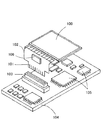
JP2010045463A - Display element, electronic element module, manufacturing method thereof, and electronic information device - Google Patents

Display element, electronic element module, manufacturing method thereof, and electronic information device Download PDF

Info

Publication number
JP2010045463A
JP2010045463A JP2008206440A JP2008206440A JP2010045463A JP 2010045463 A JP2010045463 A JP 2010045463A JP 2008206440 A JP2008206440 A JP 2008206440A JP 2008206440 A JP2008206440 A JP 2008206440A JP 2010045463 A JP2010045463 A JP 2010045463A
Authority
JP
Japan
Prior art keywords
electronic element
display
resin
lens
support substrate
Prior art date
Legal status (The legal status is an assumption and is not a legal conclusion. Google has not performed a legal analysis and makes no representation as to the accuracy of the status listed.)
Granted
Application number
JP2008206440A
Other languages
Japanese (ja)
Other versions
JP5037450B2 (en
Inventor
Yoshitaka Okita
悦崇 沖田
Shigekazu Takada
栄和 高田
Masahito Imanishi
雅人 今西
Kazuya Fujita
和弥 藤田
Current Assignee (The listed assignees may be inaccurate. Google has not performed a legal analysis and makes no representation or warranty as to the accuracy of the list.)
Sharp Corp
Original Assignee
Sharp Corp
Priority date (The priority date is an assumption and is not a legal conclusion. Google has not performed a legal analysis and makes no representation as to the accuracy of the date listed.)
Filing date
Publication date
Application filed by Sharp Corp filed Critical Sharp Corp
Priority to JP2008206440A priority Critical patent/JP5037450B2/en
Priority to US12/462,525 priority patent/US8704961B2/en
Publication of JP2010045463A publication Critical patent/JP2010045463A/en
Application granted granted Critical
Publication of JP5037450B2 publication Critical patent/JP5037450B2/en
Expired - Fee Related legal-status Critical Current
Anticipated expiration legal-status Critical

Links

Images

Classifications

    • HELECTRICITY
    • H01ELECTRIC ELEMENTS
    • H01LSEMICONDUCTOR DEVICES NOT COVERED BY CLASS H10
    • H01L27/00Devices consisting of a plurality of semiconductor or other solid-state components formed in or on a common substrate
    • H01L27/14Devices consisting of a plurality of semiconductor or other solid-state components formed in or on a common substrate including semiconductor components sensitive to infrared radiation, light, electromagnetic radiation of shorter wavelength or corpuscular radiation and specially adapted either for the conversion of the energy of such radiation into electrical energy or for the control of electrical energy by such radiation
    • H01L27/144Devices controlled by radiation
    • H01L27/146Imager structures
    • H01L27/14601Structural or functional details thereof
    • HELECTRICITY
    • H04ELECTRIC COMMUNICATION TECHNIQUE
    • H04NPICTORIAL COMMUNICATION, e.g. TELEVISION
    • H04N23/00Cameras or camera modules comprising electronic image sensors; Control thereof
    • H04N23/50Constructional details
    • H04N23/54Mounting of pick-up tubes, electronic image sensors, deviation or focusing coils
    • HELECTRICITY
    • H01ELECTRIC ELEMENTS
    • H01LSEMICONDUCTOR DEVICES NOT COVERED BY CLASS H10
    • H01L27/00Devices consisting of a plurality of semiconductor or other solid-state components formed in or on a common substrate
    • H01L27/14Devices consisting of a plurality of semiconductor or other solid-state components formed in or on a common substrate including semiconductor components sensitive to infrared radiation, light, electromagnetic radiation of shorter wavelength or corpuscular radiation and specially adapted either for the conversion of the energy of such radiation into electrical energy or for the control of electrical energy by such radiation
    • H01L27/144Devices controlled by radiation
    • H01L27/146Imager structures
    • H01L27/14601Structural or functional details thereof
    • H01L27/14625Optical elements or arrangements associated with the device
    • GPHYSICS
    • G02OPTICS
    • G02FOPTICAL DEVICES OR ARRANGEMENTS FOR THE CONTROL OF LIGHT BY MODIFICATION OF THE OPTICAL PROPERTIES OF THE MEDIA OF THE ELEMENTS INVOLVED THEREIN; NON-LINEAR OPTICS; FREQUENCY-CHANGING OF LIGHT; OPTICAL LOGIC ELEMENTS; OPTICAL ANALOGUE/DIGITAL CONVERTERS
    • G02F1/00Devices or arrangements for the control of the intensity, colour, phase, polarisation or direction of light arriving from an independent light source, e.g. switching, gating or modulating; Non-linear optics
    • G02F1/01Devices or arrangements for the control of the intensity, colour, phase, polarisation or direction of light arriving from an independent light source, e.g. switching, gating or modulating; Non-linear optics for the control of the intensity, phase, polarisation or colour 
    • G02F1/13Devices or arrangements for the control of the intensity, colour, phase, polarisation or direction of light arriving from an independent light source, e.g. switching, gating or modulating; Non-linear optics for the control of the intensity, phase, polarisation or colour  based on liquid crystals, e.g. single liquid crystal display cells
    • G02F1/133Constructional arrangements; Operation of liquid crystal cells; Circuit arrangements
    • G02F1/1333Constructional arrangements; Manufacturing methods
    • G02F1/1335Structural association of cells with optical devices, e.g. polarisers or reflectors
    • G02F1/133526Lenses, e.g. microlenses or Fresnel lenses

Abstract

<P>PROBLEM TO BE SOLVED: To achieve a further reduction of the number of parts, a reduction of the installing area, downsizing and thinning of a terminal by the improvement of the wiring efficiency, and lowering of power consumption by providing a structure in which an imaging element and also a lens are integrated on a glass substrate having a display element disposed thereon. <P>SOLUTION: Since the structure is provided, wherein a light receiving element is integrated on the glass substrate having the display element disposed thereon, and further a lens used for the light receiving element is formed as part of the glass substrate, the structure achieves the further reduction of the number of parts, the reduction of the installing area, downsizing and thinning of the terminal by the improvement of the wiring efficiency, lowering of the power consumption, and further cost reduction. <P>COPYRIGHT: (C)2010,JPO&INPIT

Description

本発明は、表示素子が配置された透明支持基板としてのガラス基板上に、被写体からの画像光を光電変換して撮像する半導体素子で構成された撮像素子を一体化させた受光素子一体型ディスプレイモジュールなどの表示素子・電子素子モジュールおよびその製造方法、この表示素子・電子素子モジュールを表示部および受光部に用いた例えばデジタルビデオカメラおよびデジタルスチルカメラなどのデジタルカメラや、画像入力カメラ、スキャナ、ファクシミリ、カメラ付き携帯電話装置、テレビジョン電話装置、テレビジョン装置や情報を表示する表示ユニットまたは表示装置などに搭載するディスプレイモジュールなどの電子情報機器に関する。   The present invention relates to a light receiving element integrated display in which an image pickup element composed of a semiconductor element that photoelectrically converts image light from a subject is imaged on a glass substrate as a transparent support substrate on which a display element is arranged. Display elements / electronic element modules such as modules and methods of manufacturing the same, digital cameras such as digital video cameras and digital still cameras, image input cameras, scanners, etc. The present invention relates to an electronic information device such as a facsimile, a camera-equipped mobile phone device, a television phone device, a television device, a display unit for displaying information, or a display module mounted on a display device.

従来の液晶表示素子や従来の固体撮像素子と、これを駆動したり信号処理するための複数の電子部品との接続配線の簡略化について、特許文献1、2として、図43〜図46を用いて詳細に説明する。   For simplification of connection wiring between a conventional liquid crystal display element and a conventional solid-state imaging element and a plurality of electronic components for driving and processing signals, Patent Documents 1 and 2 are used with reference to FIGS. Will be described in detail.

図43は、従来の液晶表示装置およびこれを接続する樹脂基板を示す斜視図である。   FIG. 43 is a perspective view showing a conventional liquid crystal display device and a resin substrate connecting the same.

図43において、液晶表示素子100とコネクタ接続部101とはフレキシブル配線基板102により折り曲げられて連結されている。このコネクタ接続部101は、コネクタ103に挿入されてコネクタ103を介して樹脂基板104のプリント配線に接続される。樹脂基板104には、コネクタ103と複数の電子部品105とが実装されてプリント配線に接続されている。また、フレキシブル配線基板102にはTCPボンデンィグ法によりドライブIC106が実装されて液晶表示素子100を駆動制御するようになっている。   In FIG. 43, the liquid crystal display element 100 and the connector connecting portion 101 are bent and connected by the flexible wiring board 102. The connector connecting portion 101 is inserted into the connector 103 and connected to the printed wiring on the resin substrate 104 via the connector 103. A connector 103 and a plurality of electronic components 105 are mounted on the resin substrate 104 and connected to printed wiring. In addition, a drive IC 106 is mounted on the flexible wiring board 102 by a TCP bonding method so as to drive and control the liquid crystal display element 100.

このように、液晶表示素子100と樹脂基板104とを別体に形成し、これらをコネクタ接続部101とコネクタ103により接続していたため、部品点数が増大し、また大型化するという問題があった。このような問題を解決するために、同じガラス基板上に、液晶表示素子103と導電パターンを形成し、導電パターンにドライブ用などの電子部品を実装した事例として図44に示している。   As described above, since the liquid crystal display element 100 and the resin substrate 104 are formed separately and are connected by the connector connecting portion 101 and the connector 103, there is a problem that the number of parts increases and the size increases. . FIG. 44 shows an example in which a liquid crystal display element 103 and a conductive pattern are formed on the same glass substrate in order to solve such a problem, and an electronic component for driving or the like is mounted on the conductive pattern.

図44は、従来の液晶表示素子と複数の電子部品を同じ樹脂基板上に実装した場合の断面図である。   FIG. 44 is a cross-sectional view when a conventional liquid crystal display element and a plurality of electronic components are mounted on the same resin substrate.

図44において、ガラス基板200の上側と下側の両面の導電パターン201をつなぐために、ガラス基板200の側面に導電パターン201aが形成されている。ガラス基板200上に液晶表示素子202が配設されており、ガラス基板200の反対側の面には、液晶表示素子202に光照射するためのバックライトである発光部203が配設されている。   In FIG. 44, a conductive pattern 201 a is formed on the side surface of the glass substrate 200 in order to connect the conductive patterns 201 on both the upper side and the lower side of the glass substrate 200. A liquid crystal display element 202 is disposed on the glass substrate 200, and a light emitting unit 203 that is a backlight for irradiating the liquid crystal display element 202 with light is disposed on the opposite surface of the glass substrate 200. .

このように、同じガラス基板200上に、液晶表示素子202と導電パターン201を形成し、この導電パターン201にドライブ用などの電子部品204を実装したため、図43の従来例の場合と比較して、接続配線手段として用いられる部品点数を削減でき、小型化を図ることができる。特に、導電パターン201と液晶表示素子202の電極とを直接接続することにより、図43のコネクタ103が不要になるので、組立接続配線作業が不要になると共に、部品点数がさらに削減される。   In this manner, the liquid crystal display element 202 and the conductive pattern 201 are formed on the same glass substrate 200, and the electronic component 204 for driving or the like is mounted on the conductive pattern 201. Therefore, compared with the conventional example of FIG. Thus, the number of parts used as connection wiring means can be reduced, and downsizing can be achieved. In particular, by directly connecting the conductive pattern 201 and the electrode of the liquid crystal display element 202, the connector 103 of FIG. 43 is unnecessary, so that assembly connection wiring work is not required and the number of parts is further reduced.

また、液晶表示素子202の代わりにCCD撮像素子を用いた場合も同様である。これを図45に示している。   The same applies when a CCD image sensor is used instead of the liquid crystal display element 202. This is shown in FIG.

図45は、従来のCCD撮像素子と複数の電子部品を同じ樹脂基板上に実装した場合の断面図である。   FIG. 45 is a cross-sectional view of a conventional CCD image sensor and a plurality of electronic components mounted on the same resin substrate.

図45では、スルーホールガラスプレス基板を用いて、ガラス基板300上に積層板300aを積層して多層構造にした例であり、ガラス基板300上にCCD撮像素子301が実装されると共にこれに接続される導体パターン302が設けられ、この積層板300aの導体パターン302上に電子部品303およびIC303aが実装されている。ガラス基板300の表面および裏面の各導体パターン302は、スルーホール304により接続されている。   FIG. 45 shows an example in which a laminated plate 300a is laminated on a glass substrate 300 using a through-hole glass press substrate to form a multilayer structure. The CCD image pickup device 301 is mounted on the glass substrate 300 and connected thereto. Conductor pattern 302 is provided, and electronic component 303 and IC 303a are mounted on conductor pattern 302 of laminated board 300a. The conductive patterns 302 on the front and back surfaces of the glass substrate 300 are connected by through holes 304.

一方、昨今のモバイル端末、例えばカメラ付携帯電話装置では、CMOSセンサまたはCCDセンサといった撮像素子とレンズを内蔵したカメラモジュール、表示装置である液晶パネルモジュール(または有機ELパネル)など、様々な半導体装置が携帯電話装置のCPU(中央演算処理装置)を介して接続されている。特に、折りたたみ式携帯電話装置では、表示面側端末からCPU(中央演算処理装置)が配置された本体側端末へ信号を引き渡すため、折りたたみヒンジ部に、FPC(Flexible Printed Circuit)などを介して信号線を配線する必要がある。表示面側端末にカメラモジュールを配置する場合は、液晶パネルモジュール(または有機ELパネル)などのFPC配線に加え、カメラモジュールのFPC配線も必要になり、配線に必要な面積、コストが高くなる。   On the other hand, in recent mobile terminals such as camera-equipped mobile phone devices, various semiconductor devices such as a camera module incorporating an image pickup element and a lens such as a CMOS sensor or a CCD sensor, a liquid crystal panel module (or an organic EL panel) as a display device, etc. Are connected via a CPU (central processing unit) of the mobile phone device. In particular, in a foldable mobile phone device, a signal is transferred from a display surface side terminal to a main body side terminal in which a CPU (Central Processing Unit) is arranged, so that a signal is sent to the folding hinge part via an FPC (Flexible Printed Circuit). It is necessary to wire. When the camera module is arranged on the display surface side terminal, the FPC wiring of the camera module is required in addition to the FPC wiring of the liquid crystal panel module (or the organic EL panel), and the area and cost required for wiring increase.

さらに、端末製造側では、部品点数の増加に伴う開発期間TATの長期化が懸念され、カメラモジュール製造側でも、端末機種毎にFPC配線のカスタマイズが必要となり、開発期間TATが長期化する。   Further, the terminal manufacturing side is concerned about the lengthening of the development period TAT accompanying an increase in the number of parts, and the camera module manufacturing side also needs to customize the FPC wiring for each terminal model, resulting in a long development period TAT.

これを解決するために、表示素子が配置されたガラス基板上に撮像素子をも一体化させた構造が特許文献2に提案されている。   In order to solve this, Patent Document 2 proposes a structure in which an imaging element is also integrated on a glass substrate on which a display element is arranged.

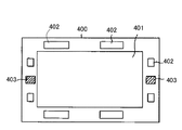
図46は、特許文献2に開示された従来の表示素子および撮像素子一体型構造を示す平面図である。   FIG. 46 is a plan view showing a conventional display element and imaging element integrated structure disclosed in Patent Document 2. As shown in FIG.

図46に示すように、従来のテレビ電話装置において、通話者の視線を一致させるために、透光性支持基板400上の中央部分に画像表示素子401が配設されており、画像表示素子401の周囲に固体撮像素子402と、ドライバーなどの駆動用半導体素子403とが配設されている。
特開平9−244007号公報 特開平5−14880号公報
As shown in FIG. 46, in a conventional videophone device, an image display element 401 is disposed at the central portion on a translucent support substrate 400 in order to match the line of sight of the caller. A solid-state image pickup element 402 and a driving semiconductor element 403 such as a driver are disposed around the periphery of each other.
JP-A-9-244007 JP-A-5-14880

上記特許文献2に開示された従来の表示素子および撮像素子一体型構造においても、更なるいっそうの部品点数の削減、実装面積の削減、配線効率の向上による端末の小型・薄型化および低消費電力化を実現することができない。   Even in the conventional display element and image pickup element integrated structure disclosed in Patent Document 2, the number of parts is further reduced, the mounting area is reduced, the wiring efficiency is improved, the terminal is reduced in size and thickness, and the power consumption is reduced. Cannot be realized.

本発明は、上記従来の問題を解決するもので、表示素子が配置されたガラス基板上に撮像素子、さらにレンズをも一体化させた構造とすることにより、更なるいっそうの部品点数の削減、実装面積の削減、配線効率の向上による端末の小型・薄型化および低消費電力化を実現できる表示素子一体型撮像素子などの表示素子・電子素子モジュールおよびその製造方法、これを表示部および受光部に用いた例えばカメラ付き携帯電話装置などの電子情報機器を提供することを目的とする。   The present invention solves the above-mentioned conventional problems, and further reduces the number of parts by adopting a structure in which an imaging element and a lens are integrated on a glass substrate on which a display element is arranged, Display element / electronic element module such as a display element-integrated image sensor that can reduce the mounting area and improve the wiring efficiency and reduce the size and thickness of the terminal, and its power consumption, and the manufacturing method thereof. An object of the present invention is to provide an electronic information device such as a camera-equipped mobile phone device used in the above.

本発明の表示素子・電子素子モジュールは、ディスプレイが配置された透光性支持基板において、該ディスプレイの配置箇所以外の透光性支持基板の一部にレンズを形成し、該レンズに対して電子素子が配置されているものであり、そのことにより上記目的が達成される。   The display element / electronic element module according to the present invention includes a light-transmitting support substrate on which a display is disposed, and a lens is formed on a part of the light-transmitting support substrate other than the position where the display is disposed. The element is arranged, and thereby the above-mentioned object is achieved.

また、好ましくは、本発明の表示素子・電子素子モジュールにおける透光性支持基板に形成されたレンズの外周側に遮光層が設けられている。   Preferably, a light shielding layer is provided on the outer peripheral side of the lens formed on the translucent support substrate in the display element / electronic element module of the present invention.

さらに、好ましくは、本発明の表示素子・電子素子モジュールにおける遮光層で囲まれた透光性支持基板上で、前記レンズの光入射用中央部以外の透光性支持基板上に金属膜などの遮光膜が設けられている。   Further preferably, on the translucent support substrate surrounded by the light shielding layer in the display element / electronic element module of the present invention, a metal film or the like is formed on the translucent support substrate other than the light incident central portion of the lens. A light shielding film is provided.

さらに、好ましくは、本発明の表示素子・電子素子モジュールにおける遮光層は、前記透光性支持基板上から形成された溝内に遮光材料が埋め込まれている。   Further preferably, in the display element / electronic element module of the present invention, the light shielding layer has a light shielding material embedded in a groove formed on the translucent support substrate.

さらに、好ましくは、本発明の表示素子・電子素子モジュールにおける遮光層は、2重または3重に平面視円形状または楕円形状、四角形状に形成された前記透光性支持基板上から形成された溝内に遮光材料が埋め込まれている。   More preferably, the light shielding layer in the display element / electronic element module of the present invention is formed on the translucent support substrate formed in a double or triple shape in a circular shape, an elliptical shape, or a rectangular shape in plan view. A light shielding material is embedded in the groove.

さらに、好ましくは、本発明の表示素子・電子素子モジュールにおける2重の遮光層の一方は、前記透光性支持基板の一方面側から形成された溝内に遮光材料が埋め込まれ、該2重の遮光層の他方は、該透光性支持基板の他方面側から形成された溝内に遮光材料が埋め込まれている。   Further preferably, in one of the double light shielding layers in the display element / electronic element module of the present invention, a light shielding material is embedded in a groove formed from one surface side of the translucent support substrate, The other light shielding layer has a light shielding material embedded in a groove formed from the other surface side of the translucent support substrate.

さらに、好ましくは、本発明の表示素子・電子素子モジュールにおける遮光用の金属膜上に絶縁膜を介して配線用の金属膜が設けられ、前記電子素子の各端子部は、該配線用の金属膜がパターニングされた配線層に接続されている。   Further preferably, a metal film for wiring is provided on the light-shielding metal film in the display element / electronic element module of the present invention via an insulating film, and each terminal portion of the electronic element is formed of the metal for wiring. The film is connected to the patterned wiring layer.

さらに、好ましくは、本発明の表示素子・電子素子モジュールにおいて、前記電子素子と前記透光性支持基板の間が遮光材料で封止されている。   Further preferably, in the display element / electronic element module of the present invention, a space between the electronic element and the translucent support substrate is sealed with a light shielding material.

さらに、好ましくは、本発明の表示素子・電子素子モジュールにおける電子素子としての撮像素子からの画像データに基づいて前記ディスプレイに直接表示するべく、該ディスプレイが前記透光性支持基板上の金属膜の配線パターンにより該撮像素子と接続される配線経路が設けられている。   Further preferably, in order to directly display on the display based on image data from an image sensor as an electronic element in the display element / electronic element module of the present invention, the display is formed of a metal film on the translucent support substrate. A wiring path connected to the imaging device is provided by a wiring pattern.

さらに、好ましくは、本発明の表示素子・電子素子モジュールにおけるレンズと前記電子素子としての受光素子の受光領域との間にIRカット材料が設けられている。   Further preferably, an IR cut material is provided between the lens in the display element / electronic element module of the present invention and the light receiving region of the light receiving element as the electronic element.

さらに、好ましくは、本発明の表示素子・電子素子モジュールにおけるIRカット材料は、前記レンズ曲面上、該レンズ曲面が形成される側とは反対の透光性支持基板面上および前記受光素子の受光領域の表面上のいずれかに設けられている。   Further preferably, the IR cut material in the display element / electronic element module of the present invention is such that the lens-curved surface, the light-transmitting support substrate surface opposite to the side on which the lens-curved surface is formed, and the light-receiving element receive light. It is provided anywhere on the surface of the region.

さらに、好ましくは、本発明の表示素子・電子素子モジュールにおける透光性支持基板のレンズは、凹型レンズおよび凸型レンズのいずれかである。   Further preferably, the lens of the translucent support substrate in the display element / electronic element module of the present invention is either a concave lens or a convex lens.

さらに、好ましくは、本発明の表示素子・電子素子モジュールにおける電子素子には、素子領域を囲む周辺領域に一または複数の電極部が配設されており、ディスプレイを構成する透光性支持基板の配線部に該電極部上の導電突起を用いて該電子素子を接続する接続構造において、該透光性支持基板と該電子素子との間の該素子領域に対応する領域を避けるように、該透光性支持基板と該電子素子との間の少なくとも該接続構造が樹脂で固められた実装構造を有する。   Further preferably, in the electronic element in the display element / electronic element module of the present invention, one or a plurality of electrode portions are disposed in a peripheral region surrounding the element region, and the translucent support substrate constituting the display is provided. In a connection structure in which the electronic element is connected to the wiring part using the conductive protrusion on the electrode part, the region corresponding to the element region between the translucent support substrate and the electronic element is avoided. It has a mounting structure in which at least the connection structure between the translucent support substrate and the electronic element is solidified with resin.

さらに、好ましくは、本発明の表示素子・電子素子モジュールにおける透光性支持基板の配線部と前記電極部上の導電突起との間に異方性導電樹脂材料の導電粒子を介在させた接続部分を完全に覆うように前記樹脂で固められている。   Further preferably, in the display element / electronic element module of the present invention, a connecting portion in which conductive particles of an anisotropic conductive resin material are interposed between the wiring portion of the translucent support substrate and the conductive protrusion on the electrode portion. Is hardened with the resin so as to completely cover.

さらに、好ましくは、本発明の表示素子・電子素子モジュールにおいて、前記透光性支持基板と前記電子素子との間の接続構造を含む周辺領域が前記樹脂で固められている。   Further preferably, in the display element / electronic element module of the present invention, a peripheral region including a connection structure between the translucent support substrate and the electronic element is hardened with the resin.

さらに、好ましくは、本発明の表示素子・電子素子モジュールにおいて、前記素子領域に対応する領域に前記樹脂が広がるのを食い止めるための突状の段差部が、前記電子素子の周辺領域、および該周辺領域に対向する前記透光性支持基板の領域のうちの少なくともいずれかに設けられている。   Further preferably, in the display element / electronic element module according to the present invention, a projecting stepped portion for preventing the resin from spreading in a region corresponding to the element region includes a peripheral region of the electronic element, and the peripheral region. It is provided in at least one of the regions of the translucent support substrate facing the region.

さらに、好ましくは、本発明の表示素子・電子素子モジュールにおいて、前記樹脂が外側に広がるのを食い止めるための突状の段差部が、前記電子素子の周辺部、および前記透光性支持基板における該電子素子と対向する領域の周辺部のうちの少なくともいずれかに設けられている。   Further preferably, in the display element / electronic element module according to the present invention, a protruding stepped portion for preventing the resin from spreading outward is provided in the peripheral portion of the electronic element and the translucent support substrate. It is provided in at least one of the peripheral portions of the region facing the electronic element.

さらに、好ましくは、本発明の表示素子・電子素子モジュールにおいて、前記素子領域に対応する領域に前記樹脂が広がるのを食い止めるべく、該樹脂をはじく性質を有する材料が、前記電子素子の周辺領域、および該周辺領域に対向する前記透光性支持基板の領域のうちの少なくともいずれかに設けられている。   Further preferably, in the display element / electronic element module of the present invention, in order to prevent the resin from spreading in a region corresponding to the element region, a material having a property of repelling the resin is a peripheral region of the electronic element, And at least one of the regions of the translucent support substrate facing the peripheral region.

さらに、好ましくは、本発明の表示素子・電子素子モジュールにおいて、前記樹脂が外側に広がるのを食い止めるべく、該樹脂をはじく性質を有する材料が、前記電子素子の周辺部、および前記透光性支持基板における該電子素子と対向する領域の周辺部のうちの少なくともいずれかに設けられている。   Further preferably, in the display element / electronic element module according to the present invention, in order to prevent the resin from spreading outward, a material having a property of repelling the resin includes a peripheral portion of the electronic element and the translucent support. It is provided in at least one of the peripheral portions of the region facing the electronic element on the substrate.

さらに、好ましくは、本発明の表示素子・電子素子モジュールにおける電子素子の周辺部は、該電子素子の端部およびその外側近傍である。   Further preferably, the peripheral portion of the electronic element in the display element / electronic element module of the present invention is an end portion of the electronic element and the vicinity thereof.

さらに、好ましくは、本発明の表示素子・電子素子モジュールにおける外側近傍の更に周辺部に封止樹脂が設けられ、該封止樹脂により前記透光性支持基板と該電子素子との間を封止している。   Further preferably, a sealing resin is provided in a further peripheral portion near the outside in the display element / electronic element module of the present invention, and the gap between the translucent support substrate and the electronic element is sealed by the sealing resin. is doing.

さらに、好ましくは、本発明の表示素子・電子素子モジュールにおける封止樹脂は、該電子素子の側面と上面を覆っている。   Further preferably, the sealing resin in the display element / electronic element module of the present invention covers the side surface and the upper surface of the electronic element.

さらに、好ましくは、本発明の表示素子・電子素子モジュールにおける突状の段差部の少なくとも表面部が、前記樹脂をはじく性質を有する材料で構成されている。   Further preferably, at least a surface portion of the projecting step portion in the display element / electronic element module of the present invention is made of a material having a property of repelling the resin.

さらに、好ましくは、本発明の表示素子・電子素子モジュールにおける樹脂は、少なくとも前記接続構造の接続部分に導電粒子を含有する樹脂が設けられている。   Further preferably, the resin in the display element / electronic element module of the present invention is provided with a resin containing conductive particles at least in the connection portion of the connection structure.

さらに、好ましくは、本発明の表示素子・電子素子モジュールにおける導電粒子を含有する樹脂材料は異方性導電樹脂材料である。   Further preferably, the resin material containing conductive particles in the display element / electronic element module of the present invention is an anisotropic conductive resin material.

さらに、好ましくは、本発明の表示素子・電子素子モジュールにおける樹脂は、非導電粒子を含有する樹脂を少なくとも一部に有する。   Further preferably, the resin in the display element / electronic element module of the present invention has at least a part of a resin containing non-conductive particles.

さらに、好ましくは、本発明の表示素子・電子素子モジュールにおける樹脂は、遮光性樹脂を少なくとも一部に有する。上記樹脂には封止樹脂も含まれる。封止樹脂の少なくとも一部に遮光性樹脂を含んでもよい。ただし、紫外線で硬化する場合は遮光性樹脂では硬化することが困難になることが多く、その場合は遮光性にしないほうが良い。   Further preferably, the resin in the display element / electronic element module of the present invention has a light-shielding resin at least in part. The resin includes a sealing resin. A light shielding resin may be included in at least a part of the sealing resin. However, in the case of curing with ultraviolet rays, it is often difficult to cure with a light-shielding resin.

さらに、好ましくは、本発明の表示素子・電子素子モジュールにおける段差部は、前記ディスプレイを構成する材料と共通材料から構成されている。   Further preferably, the step portion in the display element / electronic element module of the present invention is made of a material and a common material constituting the display.

さらに、好ましくは、本発明の表示素子・電子素子モジュールにおいて、前記樹脂をはじく材料は、前記ディスプレイを構成する材料と共通材料から構成されている。   Further preferably, in the display element / electronic element module of the present invention, the material that repels the resin is composed of a material that is common to the material that constitutes the display.

さらに、好ましくは、本発明の表示素子・電子素子モジュールにおける段差部は、前記電子素子上の膜を構成する材料と共通材料から構成されている。   Further preferably, the stepped portion in the display element / electronic element module of the present invention is made of a material common to the material constituting the film on the electronic element.

さらに、好ましくは、本発明の表示素子・電子素子モジュールにおける段差部は、電磁波により硬化する材料から構成されている。   Further, preferably, the step portion in the display element / electronic element module of the present invention is made of a material that is cured by electromagnetic waves.

さらに、好ましくは、本発明の表示素子・電子素子モジュールにおける透光性支持基板は、貫通配線または/および側面配線により接続された両面配線を有している。   Further preferably, the translucent support substrate in the display element / electronic element module of the present invention has double-sided wirings connected by through wirings and / or side wirings.

さらに、好ましくは、本発明の表示素子・電子素子モジュールにおけるディスプレイが配設されている透光性支持基板の面とは反対側の面に前記電子素子が配設され、前記両面配線を用いて該ディスプレイと該電子素子とが電気的に接続されている。   Further preferably, the electronic element is disposed on a surface opposite to the surface of the translucent support substrate on which the display in the display element / electronic element module of the present invention is disposed, and the double-sided wiring is used. The display and the electronic element are electrically connected.

さらに、好ましくは、本発明の表示素子・電子素子モジュールにおける電子素子は受光素子である。   Further preferably, the electronic element in the display element / electronic element module of the present invention is a light receiving element.

さらに、好ましくは、本発明の表示素子・電子素子モジュールにおける電子素子は、入射光を光電変換して撮像する複数の受光部が設けられた撮像素子である。   Further preferably, the electronic element in the display element / electronic element module of the present invention is an imaging element provided with a plurality of light receiving portions that photoelectrically convert incident light to image.

さらに、好ましくは、本発明の表示素子・電子素子モジュールにおける透光性支持基板は、ガラス基板または樹脂基板のいずれかである。   Further preferably, the translucent support substrate in the display element / electronic element module of the present invention is either a glass substrate or a resin substrate.

本発明の表示素子・電子素子モジュールの製造方法は、本発明の上記表示素子・電子素子モジュールの製造方法であって、前記ディスプレイが配置された透光性支持基板において、該ディスプレイの配置箇所以外の透光性支持基板の一部にレンズを形成するレンズ形成工程と、該レンズに対して電子素子を配置する電子素子配置工程とを有するものであり、そのことにより上記目的が達成される。   The method for manufacturing a display element / electronic element module according to the present invention is the method for manufacturing the display element / electronic element module according to the present invention, wherein the display device / electronic element module is a method for manufacturing the display element / electronic element module, except for the place where the display is disposed A lens forming step of forming a lens on a part of the translucent support substrate, and an electronic element arranging step of arranging an electronic element with respect to the lens, thereby achieving the above object.

また、好ましくは、本発明の表示素子・電子素子モジュールの製造方法におけるレンズ形成工程は、パターニングされたレジスト膜を熱処理した後のレジスト膜表面形状を、エッチングにより前記透光性支持基板に転写するかまたは、高温スタンパによる該透光性支持基板への押圧によってレンズ表面を形成する。   Preferably, in the method of manufacturing a display element / electronic element module according to the present invention, in the lens forming step, the resist film surface shape after heat-treating the patterned resist film is transferred to the translucent support substrate by etching. Alternatively, the lens surface is formed by pressing the translucent support substrate with a high temperature stamper.

さらに、好ましくは、本発明の表示素子・電子素子モジュールの製造方法におけるレンズ形成工程は、前記透光性支持基板から形成されたレンズに対応するように一または複数のレンズがホルダに保持された状態で固定されている。   Still preferably, in the method of manufacturing a display element / electronic element module according to the present invention, in the lens forming step, one or a plurality of lenses are held by the holder so as to correspond to the lenses formed from the translucent support substrate. It is fixed in the state.

本発明の電子情報機器は、本発明の上記表示素子・電子素子モジュールを表示部および撮像部に用いたものであり、そのことにより上記目的が達成される。   The electronic information device of the present invention uses the display element / electronic element module of the present invention for a display unit and an imaging unit, and thereby achieves the above object.

本発明の電子情報機器は、本発明の上記表示素子・電子素子モジュールを表示部、発光部および受光部に用いたものであり、そのことにより上記目的が達成される。   The electronic information device of the present invention uses the display element / electronic element module of the present invention for a display unit, a light emitting unit, and a light receiving unit, thereby achieving the above object.

上記構成により、以下、本発明の作用を説明する。   With the above configuration, the operation of the present invention will be described below.

本発明においては、ディスプレイの配置箇所以外の透光性支持基板の一部にレンズを形成し、このレンズに対して電子素子が配置されている。このように、ディスプレイ(表示素子)が配置されたガラス基板などの透光性支持基板上に電子素子(撮像素子)、さらにレンズをも一体化させた構造としている。このため、更なるいっそうの部品点数の削減、実装面積の削減、配線効率の向上による端末の小型・薄型化および低消費電力化が実現可能となる。   In the present invention, a lens is formed on a part of the translucent support substrate other than the place where the display is placed, and an electronic element is placed on this lens. As described above, an electronic element (imaging element) and a lens are integrated on a translucent support substrate such as a glass substrate on which a display (display element) is arranged. For this reason, it is possible to further reduce the number of parts, reduce the mounting area, and reduce the size and thickness of the terminal and reduce the power consumption by improving the wiring efficiency.

以上により、本発明によれば、表示素子が配置されたガラス基板上に受光素子を一体化させ、しかも、受光素子に用いるレンズをもガラス基板の一部から形成した構造とするため、更なるいっそうの部品点数の削減、実装面積の削減、配線効率の向上による端末の小型・薄型化および低消費電力化、さらにはコスト削減を実現することができる。   As described above, according to the present invention, the light receiving element is integrated on the glass substrate on which the display element is arranged, and the lens used for the light receiving element is also formed from a part of the glass substrate. It is possible to further reduce the number of parts, reduce the mounting area, improve the wiring efficiency, reduce the size and thickness of the terminal, reduce power consumption, and reduce the cost.

以下に、本発明の表示素子・電子素子モジュールおよびその製造方法の実施形態1〜3として受光素子一体型液晶ディスプレイモジュールなどの表示素子・撮像素子モジュールおよびその製造方法に適用した場合および、この表示素子・撮像素子モジュールを表示部および、受光部としての撮像部に用いた例えばカメラ付き携帯電話装置などの電子情報機器の実施形態4について図面を参照しながら詳細に説明する。   Hereinafter, the display element / electronic element module of the present invention and the manufacturing method thereof according to Embodiments 1 to 3 applied to a display element / imaging element module such as a light receiving element-integrated liquid crystal display module and the manufacturing method thereof, and this display Embodiment 4 of an electronic information device such as a mobile phone device with a camera using an element / imaging device module as a display unit and an imaging unit as a light receiving unit will be described in detail with reference to the drawings.

(実施形態1)
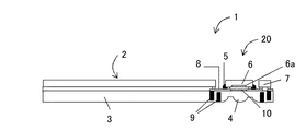
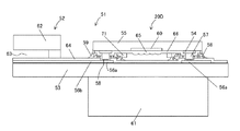
図1は、本発明の実施形態1に係る表示素子・撮像素子モジュールの要部構成例を示す縦断面図である。図2は、図1の撮像素子部分の拡大断面図である。
(Embodiment 1)
FIG. 1 is a longitudinal cross-sectional view illustrating an exemplary configuration of a main part of a display element / imaging element module according to Embodiment 1 of the present invention. FIG. 2 is an enlarged cross-sectional view of the image sensor portion of FIG.

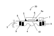
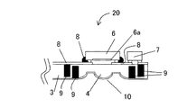
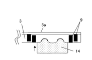
図1および図2において、本実施形態1の表示素子・撮像素子モジュール1は、表示素子一体型撮像素子(受光素子一体型ディスプレイモジュール)であり、ガラス基板3上に配置された表示装置2と、表示装置2が配置された面とは反対側の面にレンズ曲面が形成されたレンズ4と、このレンズ4の平面視外周側を遮光するための平面視2重円形状のレンズ遮光層9、9と、レンズ4に対して、表示装置2の搭載面と同じ面に受光面6aを対向させた状態で、遮光材料5でチップ周囲を封止して配置された撮像素子6と、ドライバーなどの各種電子部品であるその他の素子郡7とを有している。これらの表示装置2以外のレンズ4、遮光材料5、撮像素子6およびレンズ遮光層9、9により撮像素子モジュール20が構成されている。   1 and 2, a display element / imaging element module 1 according to the first embodiment is a display element-integrated image sensor (light-receiving element-integrated display module), and a display device 2 disposed on a glass substrate 3. The lens 4 having a lens curved surface formed on the surface opposite to the surface on which the display device 2 is disposed, and the lens light shielding layer 9 having a double circular shape in plan view for shielding the outer peripheral side in plan view of the lens 4. , 9, and the lens 4, with the light receiving surface 6 a facing the same surface as the mounting surface of the display device 2, the image pickup element 6 that is arranged by sealing the periphery of the chip with a light shielding material 5, and a driver And other element groups 7 which are various electronic components. An image sensor module 20 is configured by the lens 4, the light shielding material 5, the image sensor 6, and the lens light shielding layers 9 and 9 other than the display device 2.

即ち、表示装置2(表示素子として例えば液晶パネルや有機ELパネルなど)がガラス基板3上に配置され、表示装置2の周囲のガラス基板3の一部からレンズ4が形成されている。このレンズ4の形成面とは反対側のガラス基板1の表面に、そのレンズ4の位置と対応して、周囲が遮光材料5により封止された撮像素子6が搭載されている。この撮像素子6は、その他素子群7と共に、アルミニウムなどの遮光性のある後述する金属薄膜8c(金属配線パターン)で配線されている。その他素子群7としては、表示装置2を駆動するためのコントローラやドライバー、画像処理素子などの電子部品が挙げられるが、これらの素子群7は、ガラス基板3の外部に配置されていても構わない。   That is, the display device 2 (for example, a liquid crystal panel or an organic EL panel as a display element) is disposed on the glass substrate 3, and the lens 4 is formed from a part of the glass substrate 3 around the display device 2. On the surface of the glass substrate 1 opposite to the surface on which the lens 4 is formed, an imaging element 6 whose periphery is sealed with a light shielding material 5 is mounted corresponding to the position of the lens 4. The image pickup element 6 is wired together with the other element group 7 by a metal thin film 8c (metal wiring pattern) having a light shielding property such as aluminum described later. The other element group 7 includes electronic components such as a controller, a driver, and an image processing element for driving the display device 2, but these element groups 7 may be arranged outside the glass substrate 3. Absent.

また、これに加えて、撮像素子6の受光面6aの前方に、不要な赤外領域の波長を入射光からカットするためのIRカット材料10を設けることもできる。図1および図2では、ガラス基板3のレンズ4の形成面とは反対側の面にIRカット材料10を薄膜状にコーティングしている。また、これに限らず、図3に示すように、レンズの形成面側をIRカット材料10で薄膜状にコーティングしてもよいし、図4に示すように、撮像素子6(CMOSセンサまたはCCDセンサ)の受光部6a上に直接、IRカット材料10を薄膜状にコーティングしてもよい。   In addition to this, an IR cut material 10 for cutting the wavelength of an unnecessary infrared region from incident light can be provided in front of the light receiving surface 6a of the image sensor 6. 1 and 2, the IR cut material 10 is coated in a thin film on the surface of the glass substrate 3 opposite to the surface on which the lens 4 is formed. In addition to this, as shown in FIG. 3, the lens forming surface side may be coated with an IR cut material 10 in a thin film shape, or as shown in FIG. 4, the image sensor 6 (CMOS sensor or CCD). The IR cut material 10 may be coated in a thin film directly on the light receiving portion 6a of the sensor.

上記構成の電子素子モジュール1の製造方法について以下に説明する。   A method for manufacturing the electronic element module 1 having the above configuration will be described below.

まず、レンズ遮光層9の形成工程について説明する。レンズ遮光層9の形成工程は、図5のようにガラス基板3の一方面(後でレンズが形成されるレンズ形成面)にレジスト材料を成膜し、このレジスト材料に遮光層形成用の円形線分パターン11a(円形線分部分がレジスト剥離されたレジストパターン、楕円形線分パターンでもよい)を形成してレジスト膜11とし、その後、このレジストパターンの円形線分パターン11aが形成されたレジスト膜11をマスクとして、RIE(Reactive Ion Etching)などにより異方性エッチングを行い、図6のようなガラス基板3に遮光用の溝9aを形成する。このレジスト材料は、ノボラック系ポリマーまたはスチレン系ポリマーを用いる。このスチレン系ポリマーは透明性がよく、イメージセンサのマイクロレンズにも用いられている。また、異方性エッチングは、CHF(三フッ化メタン)ガスによるドライエッチングによりガラスエッチングを行う。 First, the formation process of the lens light shielding layer 9 will be described. As shown in FIG. 5, the lens light shielding layer 9 is formed by forming a resist material on one surface of the glass substrate 3 (a lens forming surface on which a lens will be formed later), and forming a light shielding layer on the resist material. A resist pattern 11 is formed by forming a line segment pattern 11a (a resist pattern in which a circular line segment portion is a resist strip or an elliptical line segment pattern) may be formed, and then a resist in which the circular line segment pattern 11a of this resist pattern is formed Using the film 11 as a mask, anisotropic etching is performed by RIE (Reactive Ion Etching) or the like to form a light shielding groove 9a in the glass substrate 3 as shown in FIG. As the resist material, a novolac polymer or a styrene polymer is used. This styrenic polymer has good transparency and is also used for microlenses of image sensors. In the anisotropic etching, glass etching is performed by dry etching with CHF 3 (methane trifluoride) gas.

その後、図7のように遮光材料9bによりガラス基板3の遮光用の溝9a内を埋め込む。ここで、遮光材料9bで遮光用の溝9aを埋める方法としては、例えば蒸着法が挙げられるが、この方法に限定されるものではなく、遮光材料9bにより遮光用の溝9aが埋まるかまたは、コーティングできればどの様な方法であっても構わない。   Thereafter, as shown in FIG. 7, the light shielding groove 9a of the glass substrate 3 is filled with the light shielding material 9b. Here, as a method of filling the light shielding groove 9a with the light shielding material 9b, for example, an evaporation method may be mentioned, but the method is not limited to this, and the light shielding groove 9a is filled with the light shielding material 9b or Any method can be used as long as it can be coated.

さらに、アセトンや硫酸過水などのレジスト剥離液により不要なレジスト材料を溶かしてレジスト膜11を除去し、さらに、例えばCMP(Chemical Mechanical Polishing)などの研磨方法により、不要な遮光材料9bを除去してレンズ遮光層9の形成面を平坦化し、図8のような平面視円形のレンズ遮光層9を得る。   Further, the resist film 11 is removed by dissolving an unnecessary resist material with a resist stripping solution such as acetone or sulfuric acid / hydrogen peroxide, and the unnecessary light shielding material 9b is removed by a polishing method such as CMP (Chemical Mechanical Polishing). Thus, the surface on which the lens light shielding layer 9 is formed is flattened to obtain a lens light shielding layer 9 having a circular shape in plan view as shown in FIG.

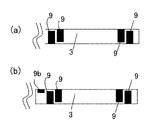
前記した場合と同様の方法で、図9(a)のようにレンズ遮光層9の形成面とは反対側の面(後に撮像素子が配置される面)に、図8で説明したレンズ遮光層9よりも径が一回り大きな平面視円形のレンズ遮光層9を形成する。ここで、内側のレンズ遮光層9と外側の平面視円形状または楕円形状のレンズ遮光層9との間隔は遮光効率、ガラス基板強度などを勘案して最適な条件で形成すればよい。   In the same manner as described above, the lens light-shielding layer described in FIG. 8 is formed on the surface opposite to the surface on which the lens light-shielding layer 9 is formed as shown in FIG. The lens light-shielding layer 9 having a circular shape in plan view that is one diameter larger than 9 is formed. Here, the distance between the inner lens light-shielding layer 9 and the outer planar light-shielding or elliptical lens light-shielding layer 9 may be formed under optimum conditions in consideration of light shielding efficiency, glass substrate strength, and the like.

なお、これらの2重のレンズ遮光層9、9の図9(a)の左下側には、図示しない液晶表示用のバックライトが配設されており、そのバックライトからの光をより確実に遮光する必要がある。このため、図9(b)に示すように、ガラス基板3の強度に影響しない浅い平面視円形状または楕円形状のレンズ遮光層9bが、外側のレンズ遮光層9の隙間を覆うように更に外周側に設けれている。また、図10(a)に示すように内側のレンズ遮光層9を外側に、外側のレンズ遮光層9を内側に入れ替えて配設することもできる。外側のレンズ遮光層9に比べて浅いレンズ遮光層9bを設ける場合には、図10(b)に示すように外側のレンズ遮光層9の隙間を覆うようにするために、レンズ曲面形成面とは反対側の面側から設けられる。   In addition, a backlight for liquid crystal display (not shown) is disposed on the lower left side of FIG. 9A of these double lens light-shielding layers 9 and 9, and the light from the backlight is more reliably transmitted. It is necessary to shield the light. For this reason, as shown in FIG. 9B, the outer periphery of the lens light-shielding layer 9b having a shallow circular shape or elliptical shape that does not affect the strength of the glass substrate 3 covers the gap between the outer lens light-shielding layers 9. On the side. Further, as shown in FIG. 10A, the inner lens light-shielding layer 9 may be disposed outside and the outer lens light-shielding layer 9 may be replaced inside. When the lens light-shielding layer 9b shallower than the outer lens light-shielding layer 9 is provided, in order to cover the gap between the outer lens light-shielding layers 9 as shown in FIG. Are provided from the opposite surface side.

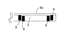
さらに、外側のレンズ遮光層9の形成面側のガラス基板3上に、図示しない金属薄膜8aを、遮光用として、図11に示すように少なくとも外側の円形または楕円形のレンズ遮光層9の内側上を覆うように形成し、内側および外側の2重のレンズ遮光層9、9および金属薄膜8aが形成されたガラス基板3を得る。なお、2重のレンズ遮光層9、9の形成方法および形状は、上記記載の平面視円形のものに限定するものではなく、レンズ外周からの光の入射、特に左下側のバックライトからの光を防止できれば、どの様な方法および形状(例えば平面視矩形状または正方形状)であっても構わない。また、以降の説明で、内側のレンズ遮光層9と外側のレンズ遮光層9とを区別する場合以外は、まとめてレンズ遮光層9として説明する。
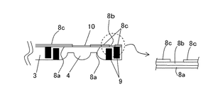
   Further, on the glass substrate 3 on the side where the outer lens light-shielding layer 9 is formed, a metal thin film 8a (not shown) is used for light shielding, and at least the inner side of the outer circular or elliptical lens light-shielding layer 9 as shown in FIG. A glass substrate 3 is obtained which is formed so as to cover the top and on which the inner and outer double lens light-shielding layers 9 and 9 and the metal thin film 8a are formed. The formation method and shape of the double lens light-shielding layers 9 and 9 are not limited to the circular shape in plan view described above, but light incident from the outer periphery of the lens, particularly light from the lower left backlight. Any method and shape (for example, a rectangular shape or a square shape in plan view) may be used. Further, in the following description, the lens light shielding layer 9 will be collectively described unless the inner lens light shielding layer 9 and the outer lens light shielding layer 9 are distinguished.

また、ガラス基板3上への遮光用の金属薄膜8aの形成は、図12に示すように、その上の絶縁膜8bを介した配線用の金属薄膜8cのパターニングが必要となる工程の直前に形成しても構わない。むしろ、最初に金属薄膜8aを形成する場合、それ以降の工程で金属薄膜8aを熱や薬液から保護しなければならない工程が発生するため、金属薄膜8aの形成はその上の金属薄膜8cのパターニングが必要となる工程の直前に行う方が望ましいが、ここでは説明の便宜上、金属薄膜8aだけを最初に形成した場合について説明している。なお、金属薄膜8aの保護が必要な工程においても、ここでは、その説明を割愛するが、実際の工程では必要に応じて金属薄膜8aの保護を行えばよい。これらの金属薄膜8a、絶縁膜8bおよび金属薄膜8cからなる3層の金属多層膜8の膜厚は、図12では、説明を簡略化するために厚く図示しているが、実際は、図11の金属薄膜8aと図12の金属多層膜8の各膜厚が互いに同程度である。   In addition, as shown in FIG. 12, the light-shielding metal thin film 8a is formed on the glass substrate 3 immediately before the process that requires the patterning of the metal thin film 8c for wiring through the insulating film 8b thereon. It may be formed. Rather, when the metal thin film 8a is formed first, there is a process in which the metal thin film 8a must be protected from heat and chemicals in subsequent processes. Therefore, the metal thin film 8a is formed by patterning the metal thin film 8c thereon. However, for convenience of explanation, the case where only the metal thin film 8a is formed first is described here. In addition, in the process which needs protection of the metal thin film 8a, the description is omitted here, but in the actual process, the metal thin film 8a may be protected as necessary. The thickness of the three-layered metal multilayer film 8 composed of the metal thin film 8a, the insulating film 8b, and the metal thin film 8c is shown thick in FIG. 12 to simplify the description. Each film thickness of the metal thin film 8a and the metal multilayer film 8 of FIG. 12 is comparable.

次に、ガラス基板3の一方面にレンズ曲面形状を形成するレンズ形成工程について説明する。このレンズ形成工程は、レンズ4、ここでは凸型レンズの場合について説明する。図13(a)および図13(b)のように、金属薄膜8aの形成面(ガラス基板3の他方面)とは反対側の面に、レジスト材料を成膜し、これにレンズ形成用の円形線分パターン12a(楕円形線分パターンでもよい)を形成してレジスト膜12とする。このレジスト膜12には、円形線分パターン12aの円形線分部分がレジスト剥離されたレジストパターンが形成されており、内側のレンズ遮光層9よりも更に内側に円形線分パターン12aがパターニングされている。このレジスト材料は、ノボラック系ポリマーまたはスチレン系ポリマーを用いる。このスチレン系ポリマーは透明性がよく、イメージセンサのマイクロレンズにも用いられている。   Next, a lens forming process for forming a lens curved surface shape on one surface of the glass substrate 3 will be described. This lens forming step will be described for the case of the lens 4, here a convex lens. As shown in FIGS. 13A and 13B, a resist material is formed on the surface opposite to the surface on which the metal thin film 8a is formed (the other surface of the glass substrate 3), and this is used for lens formation. A circular line segment pattern 12 a (which may be an elliptical line segment pattern) is formed to form a resist film 12. The resist film 12 is formed with a resist pattern in which the circular line segment portion of the circular line segment pattern 12a is peeled off. The circular line segment pattern 12a is patterned further inside than the inner lens light-shielding layer 9. Yes. As the resist material, a novolac polymer or a styrene polymer is used. This styrenic polymer has good transparency and is also used for microlenses of image sensors.

その後の熱処理により、図14のように、円形線分パターン12aが形成されたレジスト膜12の端縁部分(角部分)に丸みを与えて、中央部分の平面視円形状のレジスト材料をその表面が球面状のレンズ形状4aに硬化させる。このレジスト材料の熱硬化条件は、例えば摂氏175度程度で数分間行う。   By subsequent heat treatment, the edge portion (corner portion) of the resist film 12 on which the circular line segment pattern 12a is formed is rounded as shown in FIG. Is cured into a spherical lens shape 4a. The resist material is thermally cured at, for example, about 175 degrees Celsius for several minutes.

これに対して、レジスト材料とガラス基板3のエッチングレートが等しくなるエッチング条件でRIE(Reactive Ion Etching)による異方性エッチングを行う。異方性エッチングは、CHF(三フッ化メタン)ガスによるドライエッチングにより行う。 On the other hand, anisotropic etching by RIE (Reactive Ion Etching) is performed under an etching condition in which the etching rates of the resist material and the glass substrate 3 are equal. The anisotropic etching is performed by dry etching with CHF 3 (methane trifluoride) gas.

これによって、図15のように、ガラス基板3の一方面上にレジストパターンの表面形状が転写された凸型のレンズ4が形成されている。この熱硬化によるレジスト材料の球面形状加工(凸型レンズ面加工)は、レジスト材料の組成や熱処理温度(摂氏175度程度)・時間(数分間)を制御して最適な形状が得られるように調整する。   As a result, as shown in FIG. 15, a convex lens 4 having the surface shape of the resist pattern transferred onto one surface of the glass substrate 3 is formed. The spherical shape processing (convex lens surface processing) of the resist material by thermosetting is such that the optimal shape can be obtained by controlling the composition of the resist material, the heat treatment temperature (about 175 degrees Celsius), and the time (several minutes). adjust.

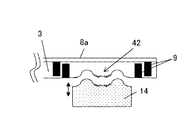
一方、レンズ4として、例えば図18に示すような凹型レンズ41を形成する場合には、図16(a)および図16(b)のようにガラス基板3上に積層された金属薄膜8a側の面とは反対側の面(下面)に、凹型レンズ41の中心光軸がレジスト材料によるレンズ形成用の円形パターン13a(円形部分がレジスト剥離液より剥離されたパターン、楕円形部分がレジスト剥離液より剥離されたパターンでもよい)の中心に位置するように円形パターン13aを形成してレジストパターン13とする。この円形パターン13aの中心は円形状のレンズ遮光層9の中心とも一致している。その後、図17のように、RIE(Reactive Ion Etching)またはウェットエッチングによりガラス基板3を等方性エッチングする。ウェットエッチングによる等方性エッチングは、BHF(バッファードフッ酸)により行う。   On the other hand, when the concave lens 41 as shown in FIG. 18 is formed as the lens 4, for example, the metal thin film 8a side laminated on the glass substrate 3 as shown in FIGS. 16 (a) and 16 (b). On the surface (lower surface) opposite to the surface, the central optical axis of the concave lens 41 is a circular pattern 13a for forming a lens made of a resist material (a pattern in which a circular portion is peeled from a resist stripping solution, and an elliptical portion is a resist stripping solution. A circular pattern 13a is formed so as to be positioned at the center of the pattern (which may be a more peeled pattern). The center of the circular pattern 13a also coincides with the center of the circular lens light-shielding layer 9. Thereafter, as shown in FIG. 17, the glass substrate 3 is isotropically etched by RIE (Reactive Ion Etching) or wet etching. Isotropic etching by wet etching is performed with BHF (buffered hydrofluoric acid).

そのエッチング後に、図18に示すようにレジスト剥離液によりレジストパターン13を除去し、凹型レンズ41の形成が完了する。この凹型レンズ41の大きさは、レジストパターン13における円形パターン13aの直径、エッチング時間に比例するため、配置する撮像素子(CCDセンサまたはCMOSセンサ)の光学サイズに合せて、レジストパターン13における円形パターン13aの直径とエッチング時間を最適なエッチング条件に制御すればよい。   After the etching, the resist pattern 13 is removed with a resist stripping solution as shown in FIG. 18, and the formation of the concave lens 41 is completed. Since the size of the concave lens 41 is proportional to the diameter of the circular pattern 13a in the resist pattern 13 and the etching time, the circular pattern in the resist pattern 13 is matched to the optical size of the image pickup device (CCD sensor or CMOS sensor) to be arranged. What is necessary is just to control the diameter and etching time of 13a to optimal etching conditions.

また、図19〜図21のように、高温スタンパ14を使用して、ガラス基板3の下面を押圧しても、高温スタンパ14のレンズ形状をガラス基板3の下面に転写することができる。この場合、高温スタンパ14の形状を任意に変えることにより、例えば図20のようなフレネルレンズのレンズ形状42を自由度高く形成することも可能となる。レンズ形成方法は、上記のエッチングや高温スタンパ14による方法に限定するものではなく、ガラス基板3を凹型または凸型、更にはフレネル形状などの所定のレンズ形状に形成できれば、どのようなレンズ形成方法であっても構わない。この場合の高温スタンパ14の温度はガラス屈伏点温度かまたはその付近の温度である。このガラス屈伏点温度は、ガラス材料の種類により異なっている。   Further, as shown in FIGS. 19 to 21, the lens shape of the high temperature stamper 14 can be transferred to the lower surface of the glass substrate 3 even if the high temperature stamper 14 is used to press the lower surface of the glass substrate 3. In this case, by arbitrarily changing the shape of the high temperature stamper 14, for example, the lens shape 42 of the Fresnel lens as shown in FIG. 20 can be formed with a high degree of freedom. The lens forming method is not limited to the method using the etching or the high temperature stamper 14 described above, and any lens forming method can be used as long as the glass substrate 3 can be formed into a predetermined lens shape such as a concave shape or a convex shape, or a Fresnel shape. It does not matter. In this case, the temperature of the high temperature stamper 14 is the glass yield point temperature or a temperature in the vicinity thereof. This glass yield point temperature varies depending on the type of glass material.

さらに、レンズ遮光層9の形成工程と、レンズ4の形成工程とはその順序を限定するものではなく、順序の入れ替えや、工程の統合を行っても構わない。以降、本文において、レンズ形状を明確に区別するとき以外は単にレンズ4と記載する。また、説明図では、凸型のレンズ4で記載するが、これに限定するものではなく、凹型のレンズ形状41、さらには、フレネル形状のレンズ形状42であっても構わない。   Furthermore, the order of the formation process of the lens light shielding layer 9 and the formation process of the lens 4 are not limited, and the order may be changed or the processes may be integrated. Hereinafter, the term “lens 4” is used in the text except when the lens shape is clearly distinguished. In the explanatory diagram, the convex lens 4 is described, but the present invention is not limited to this, and a concave lens shape 41 or a Fresnel-shaped lens shape 42 may be used.

次に、IRカット材料10をレンズ形成面側のガラス基板3にコーティングする場合は、図22のようにレンズ形成面側のガラス基板全体にIRカット材料10を薄膜状にコーティングし、必要に応じて、不要なIRカット材料10を除去する場合は、図23のようなレジストパターン15(IRカット材料10を除去する部分15aがレジスト剥離されたパターン)をレンズ4の形成面にパターニングし、レジストパターン15をマスクとして、IRカット材料10をガラス基板3から除去し、その後、レジスト剥離液によりレジスト材料を除去して、図24のようなIRカット材料10の形状を得る。   Next, when the IR cut material 10 is coated on the glass substrate 3 on the lens forming surface side, the IR cut material 10 is coated in a thin film on the entire glass substrate on the lens forming surface side as shown in FIG. When the unnecessary IR cut material 10 is removed, a resist pattern 15 (a pattern in which the portion 15a from which the IR cut material 10 is removed is removed) as shown in FIG. Using the pattern 15 as a mask, the IR cut material 10 is removed from the glass substrate 3, and then the resist material is removed with a resist stripping solution to obtain the shape of the IR cut material 10 as shown in FIG.

ここでは、便宜上、図24のようにIRカット材料10のパターニングを行ったが、IRカット材料10が不要な部分が無ければ、パターニングする必要はない。   Here, for convenience, the IR cut material 10 is patterned as shown in FIG. 24. However, if there is no portion where the IR cut material 10 is unnecessary, the patterning is not necessary.

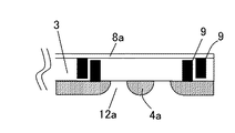
また、レンズ形成面とは反対側の面(金属薄膜8aが積層されている面)にIRカット材料10をコーティングする場合は、図25(a)に示すように、撮像素子6の受光面6aよりも一回り大きなレジスト矩形パターン16aを形成し、レジスト矩形パターン16aが形成されたレジストパターン16をマスクとして、先ず、ガラス基板3上に積層された金属薄膜8aをエッチングし、次いで、図25(b)に示すようにIRカット材料10をコーティングする。その後、レジストパターン16を除去して、図26のようなIRカット材料10の形状を得る。撮像素子6の受光面6aとIRカット材料10のコーティング面の配置関係、形状の例は図28に示している。   When the IR cut material 10 is coated on the surface opposite to the lens forming surface (the surface on which the metal thin film 8a is laminated), as shown in FIG. 25A, the light receiving surface 6a of the image sensor 6 is used. First, the metal thin film 8a laminated on the glass substrate 3 is etched using the resist pattern 16 on which the resist rectangular pattern 16a is formed as a mask. The IR cut material 10 is coated as shown in b). Thereafter, the resist pattern 16 is removed to obtain the shape of the IR cut material 10 as shown in FIG. FIG. 28 shows an example of the arrangement relationship and shape between the light receiving surface 6a of the image sensor 6 and the coating surface of the IR cut material 10.

このように、金属薄膜8aが積層されている面にIRカット材料10を薄膜状にコーティングする場合は、金属薄膜8a自体が赤外を含む入射光全体を遮光する役割を果たすため、レンズ4による集光後の光に対して、撮像素子6の受光面6aに入射する経路のみ、IRカット材料10を薄膜状にコーティングすればよいのに対して、レンズ4の形成面側にIRカット材料10を薄膜状にコーティングする場合は、レンズ集光後の光に赤外成分が混入しないように、レンズ遮光層9より内側に入射する光全体に対して赤外成分のカットを行うように、IRカット材料10をコーティングする必要があり、それぞれIRカット材料10を薄膜状にコーティングするガラス基板面に対して、最適なコーティングパターンを形成する。IRカット材料10をコーティングする方法は例えば蒸着法が挙げられるが、この方法に限定するものではなく、均一膜厚でIRカット材料10がコーティングできれば、どの様な方法であっても構わない。また、IRカット材料10のパターニングは前記方法および形状に限定するものではなく、撮像面に入射する赤外成分をカットできれば、どのような方法であっても構わない。なお、撮像素子6に直接、IRカット材料10をコーティングする場合はこの工程は省略される。   Thus, when the IR cut material 10 is coated in a thin film on the surface on which the metal thin film 8a is laminated, the metal thin film 8a itself plays a role of shielding the entire incident light including infrared rays. The IR cut material 10 may be coated in a thin film only on the path incident on the light receiving surface 6a of the image sensor 6 with respect to the condensed light, whereas the IR cut material 10 is formed on the lens 4 forming surface side. Is coated in a thin film shape, the IR component is cut so that the entire light incident on the inner side of the lens light-shielding layer 9 is cut so that the infrared component is not mixed into the light after the lens is condensed. The cutting material 10 needs to be coated, and an optimum coating pattern is formed on the glass substrate surface on which the IR cutting material 10 is coated in a thin film. The method for coating the IR cut material 10 includes, for example, a vapor deposition method, but is not limited to this method, and any method may be used as long as the IR cut material 10 can be coated with a uniform film thickness. The patterning of the IR cut material 10 is not limited to the above method and shape, and any method may be used as long as the infrared component incident on the imaging surface can be cut. Note that this step is omitted when the IR cut material 10 is directly coated on the image sensor 6.

次に、図27に示すように、遮光用の金属薄膜8a上に絶縁膜8bを形成し、その上に配線用の金属薄膜8cを形成する。さらに、表示装置2と撮像素子6およびその他素子群7を配線するための金属薄膜8cの配線パターンを形成する。この配線パターン形成工程は、前記のレンズ形成またはIRカット材料コーティング工程と同じく、レジストパターニングとRIEまたはウェットエッチングなどにより金属薄膜8cを所定の配線パターンにパターニングする。エッチング方法は、これらに限定されるものではなく、金属薄膜8cの配線のパターニングができればどのような方法であっても構わない。   Next, as shown in FIG. 27, an insulating film 8b is formed on the light shielding metal thin film 8a, and a wiring metal thin film 8c is formed thereon. Further, a wiring pattern of a metal thin film 8 c for wiring the display device 2, the image sensor 6 and the other element group 7 is formed. In this wiring pattern forming step, the metal thin film 8c is patterned into a predetermined wiring pattern by resist patterning and RIE or wet etching, as in the lens forming or IR cut material coating step. The etching method is not limited to these, and any method may be used as long as the wiring of the metal thin film 8c can be patterned.

なお、前記のIRカット材料コーティング工程と金属配線パターニング工程はその順序を限定するものではなく、順序の入れ替えや、工程の統合を行っても構わない。   The order of the IR cut material coating process and the metal wiring patterning process is not limited, and the order may be changed or the processes may be integrated.

最後に、金属薄膜8cの配線パターンに合せて、各素子を接続し図1に示す撮像装置が完成する。   Finally, each element is connected in accordance with the wiring pattern of the metal thin film 8c to complete the imaging device shown in FIG.

各素子の接続方法は例えば、FCB(Flip Chip Bond)などが挙げられるが、これに限定するものではなく、電気的に各素子と金属薄膜8cの配線パターンとを接続できればどの様な方法であっても構わない。ただし、撮像素子6(CMOSセンサまたはCCDセンサ)を接続する際には、図28のように、ガラス基板3と撮像素子6との間のギャップを遮光材料5で封止し、接続部側から光が入らないように遮光する。このギャップを封止する方法は、異方性導電接着材であるACP(AnisotropicConductive Paste)などの熱硬化樹脂による封止方法が考えられるが、これに限定されるものではなく、接続面の電気的接続を保持したまま、遮光できれば、どの様な方法であっても構わない。なお、レンズ遮光層9に使用する遮光材料と撮像素子6の封止に使用する遮光材料5とは、異なる素材を使用してもよいし、同じ素材を使用してもよく、本発明による撮像装置を形成する工程に合せて、それぞれ最適な材料を使用すればよい。   The connection method of each element includes, for example, FCB (Flip Chip Bond), but is not limited to this, and any method can be used as long as each element can be electrically connected to the wiring pattern of the metal thin film 8c. It doesn't matter. However, when connecting the image sensor 6 (CMOS sensor or CCD sensor), the gap between the glass substrate 3 and the image sensor 6 is sealed with a light shielding material 5 as shown in FIG. Shield from light. A method for sealing the gap may be a sealing method using a thermosetting resin such as ACP (Anisotropic Conductive Paste) which is an anisotropic conductive adhesive, but is not limited to this, and the electrical connection surface is electrically connected. Any method may be used as long as the light can be shielded while maintaining the connection. Note that the light shielding material used for the lens light shielding layer 9 and the light shielding material 5 used for sealing the imaging element 6 may be made of different materials or the same material. An optimum material may be used in accordance with the process of forming the device.

なお、上記実施形態1では、1枚のレンズ4を用いる場合について説明したが、これに限らず、光学性能に合せて、ガラス基板3のレンズ4に加えて、図29のように、別の一または複数のレンズ群、例えば2枚のレンズ群17Aをレンズ4に対向配置して組み合わせた構成とすることもできる。この場合、撮像素子モジュール20Aとして、一または複数のレンズ群、ここでは2枚のレンズ群17Aを円筒状で遮光性のあるレンズホルダー17B内に保持し、2枚のレンズ群17Aと共にレンズホルダー17Bをガラス基板3のレンズ4に対向させて配置する。この場合、レンズホルダー17Bの位置と、内側のレンズ遮光層9の位置とを一致させて遮光性を確保させる必要がある。また、レンズホルダー17B内に保持された2枚のレンズ群17Aに限らず、図30のように、撮像素子モジュール20Bとして、一または複数のレンズ群として、ここでは、他の種類の2枚のレンズ群18Aがそれぞれ、レンズ部の周囲のこば部を2枚重ね合わせ、レンズ4に対応させて各こば部を順次重ねて接着し、その上から遮光部材18B(遮光ホルダ)を被せて接着している。   In addition, although the case where the one lens 4 was used was demonstrated in the said Embodiment 1, in addition to this, in addition to the lens 4 of the glass substrate 3 according to optical performance, as shown in FIG. One or a plurality of lens groups, for example, two lens groups 17 </ b> A may be arranged so as to face the lens 4 and combined. In this case, as the image sensor module 20A, one or a plurality of lens groups, here two lens groups 17A, are held in a cylindrical light-shielding lens holder 17B, and the lens holder 17B together with the two lens groups 17A. Is disposed so as to face the lens 4 of the glass substrate 3. In this case, it is necessary to ensure the light shielding property by matching the position of the lens holder 17B with the position of the inner lens light shielding layer 9. In addition to the two lens groups 17A held in the lens holder 17B, as shown in FIG. 30, as the image sensor module 20B, as one or a plurality of lens groups, here, two other types of two lenses are used. Each of the lens groups 18 </ b> A overlaps two optical fiber parts around the lens part, and sequentially attaches the optical fiber parts corresponding to the lens 4, and covers the light-shielding member 18 </ b> B (light-shielding holder) from above. Glued.

(実施形態2)
上記実施形態1では、表示装置2の表示画面の向きと撮像素子モジュール20が撮像する向きとが逆の場合について説明したが、本実施形態2では、表示装置2の表示画面の向きと、後述する撮像素子モジュール20Cが入射光を取り込んで撮像する向きとが同じ場合について説明する。
(Embodiment 2)
In the first embodiment, the case where the orientation of the display screen of the display device 2 is opposite to the orientation in which the imaging element module 20 captures an image has been described. However, in the present embodiment 2, the orientation of the display screen of the display device 2 is described later. A case will be described in which the imaging element module 20 </ b> C that captures incident light has the same direction for capturing an image.

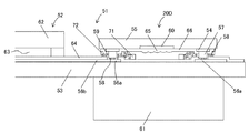
図31は、本発明の実施形態2に係る表示素子・撮像素子モジュールの要部構成例を示す縦断面図である。   FIG. 31 is a longitudinal cross-sectional view illustrating an exemplary main configuration of a display element / imaging element module according to Embodiment 2 of the present invention.

図31において、本実施形態2の表示素子・撮像素子モジュール1Aは、表示素子一体型撮像素子であり、ガラス基板3上に配置された表示装置2と、表示装置2が配置された面と同じ面にレンズ曲面が形成されたレンズ4と、このレンズ4の平面視外周側を遮光するための平面視2重円形状のレンズ遮光層9、9と、レンズ4に対して、表示装置2の搭載面とは反対側の面(下面)に受光面6aを対向させた状態で、遮光材料5でチップ周囲を封止して配置された撮像素子6と、撮像素子6が配置される側の面に搭載されたドライバーなどの各種電子部品であるその他の素子郡7とを有している。これらの表示装置2以外のレンズ4、遮光材料5、撮像素子6およびレンズ遮光層9、9により撮像素子モジュール20Cが構成されている。   In FIG. 31, the display element / imaging element module 1 </ b> A of the second embodiment is a display element-integrated image sensor, and is the same as the display device 2 disposed on the glass substrate 3 and the surface on which the display device 2 is disposed. The lens 4 having a curved surface on the surface, the planar light shielding layers 9 and 9 for shielding the outer periphery of the lens 4 in plan view, and the lens 4, In a state where the light receiving surface 6a is opposed to the surface (lower surface) opposite to the mounting surface, the image pickup device 6 arranged by sealing the periphery of the chip with the light shielding material 5, and the side on which the image pickup device 6 is arranged It has other element groups 7 which are various electronic parts such as a driver mounted on the surface. An image sensor module 20 </ b> C is configured by the lens 4, the light shielding material 5, the image sensor 6, and the lens light shielding layers 9 and 9 other than the display device 2.

即ち、表示装置2(表示素子として例えば液晶パネルや有機ELパネルなど)がガラス基板3上に配置され、表示装置2の周囲のガラス基板3の一部からレンズ4が形成されている。このレンズ4の形成面(上面)とは反対側のガラス基板1の下面に、そのレンズ4の位置と対応して、周囲が遮光材料5により封止された撮像素子6が搭載されている。この撮像素子6は、その他素子群7と共に、アルミニウムなどの遮光性のある後述する金属薄膜8aを含む多層配線パターン8で配線されている。その他素子群7としては、表示装置2を駆動するためのコントローラやドライバー、画像処理素子などの電子部品が挙げられるが、これらの素子群7は、ガラス基板3の外部に配置されていても構わない。   That is, the display device 2 (for example, a liquid crystal panel or an organic EL panel as a display element) is disposed on the glass substrate 3, and the lens 4 is formed from a part of the glass substrate 3 around the display device 2. An imaging element 6 whose periphery is sealed with a light shielding material 5 is mounted on the lower surface of the glass substrate 1 opposite to the surface (upper surface) of the lens 4 corresponding to the position of the lens 4. The imaging element 6 is wired together with the other element group 7 by a multilayer wiring pattern 8 including a metal thin film 8a having a light shielding property such as aluminum described later. The other element group 7 includes electronic components such as a controller, a driver, and an image processing element for driving the display device 2, but these element groups 7 may be arranged outside the glass substrate 3. Absent.

上記実施形態1,2によれば、表示装置2が配置されるガラス基板3上にレンズ4を形成し、このレンズ4のレンズ形成部に撮像素子6を配置することで、カメラモジュールである撮像素子モジュール20および20A〜20Cのいずれかの構成素子であるレンズ4、撮像素子6を表示装置2が配置されるガラス基板3上に一体化している。レンズ4は表示装置2のガラス基板3を兼用しているため、レンズ4の1枚分の材料費および高さ(嵩)を削減できる。また、撮像素子6をガラス基板3上の金属薄膜8の配線で接続して、表示装置2からの金属薄膜配線と、金属薄膜8cの配線とをまとめてガラス基板3上で一つの信号配線群にすることで、入出力用のFPCを1本化し、配線効率を高め、端末の小型化とコスト削減を実現できる。さらに、撮像素子6と表示装置2を一体化することにより、本体CPU(中央演算処理装置;制御部)を介さずに撮像素子6から表示装置2に直接表示させることも可能となり、表示装置2の表示画面上への高速描画と低消費電力化を実現できる。さらに、端末製造側では、カメラモジュールである撮像素子モジュール20および20A〜20Cのいずれかの実装工程が削減でき、TAT短縮が可能となる。また、カメラモジュール製造側では、ガラス基板3上のレンズ4のサイズ、配線パターンを変更するだけで様々な光学サイズの撮像素子6に対応でき、端末機種毎のFPC配線のカスタマイズから開放される。さらに、撮像素子6の端子位置を規格化することで、配線パターンの変更からも開放され、レンズ4のサイズの変更のみで済むようになる。   According to the first and second embodiments, the lens 4 is formed on the glass substrate 3 on which the display device 2 is disposed, and the imaging element 6 is disposed on the lens forming portion of the lens 4, thereby imaging the camera module. The element 4 and the lens 4 and the imaging element 6 which are constituent elements of the element modules 20A to 20C are integrated on the glass substrate 3 on which the display device 2 is arranged. Since the lens 4 also serves as the glass substrate 3 of the display device 2, the material cost and height (bulk) of one lens 4 can be reduced. In addition, the imaging element 6 is connected by the wiring of the metal thin film 8 on the glass substrate 3, and the metal thin film wiring from the display device 2 and the wiring of the metal thin film 8 c are combined into one signal wiring group on the glass substrate 3. By doing so, the number of FPCs for input / output can be unified, the wiring efficiency can be improved, and the terminal can be downsized and the cost can be reduced. Further, by integrating the image pickup device 6 and the display device 2, it is possible to directly display the image on the display device 2 from the image pickup device 6 without using the main body CPU (central processing unit; control unit). High-speed drawing on the display screen and low power consumption can be realized. Furthermore, on the terminal manufacturing side, the mounting process of any of the image sensor modules 20 and 20A to 20C, which are camera modules, can be reduced, and TAT can be shortened. Further, on the camera module manufacturing side, it is possible to cope with the image pickup device 6 of various optical sizes only by changing the size of the lens 4 on the glass substrate 3 and the wiring pattern, and it is free from customization of FPC wiring for each terminal model. Furthermore, by standardizing the terminal position of the image sensor 6, it is freed from changing the wiring pattern, and only the size of the lens 4 needs to be changed.

なお、遮光層9で囲まれた透光性支持基板上で、レンズの光入射用中央部以外の透光性支持基板上に遮光用の金属層として金属薄膜8aを設けたが、これに限らず、カーボンを含有した遮光用の導電薄膜であってもよいし、遮光性を有する絶縁膜であってもよく、遮光膜であればよい。   In addition, on the translucent support substrate surrounded by the light shielding layer 9, the metal thin film 8a is provided as the light shielding metal layer on the translucent support substrate other than the light incident central portion of the lens. Alternatively, it may be a light-shielding conductive thin film containing carbon, a light-shielding insulating film, or any light-shielding film.

(実施形態3)
図32は、本発明の実施形態3に係る受光素子一体型液晶ディスプレイモジュールの構成例を示す要部断面図である。
(Embodiment 3)
FIG. 32 is a cross-sectional view of a main part showing a configuration example of a light receiving element-integrated liquid crystal display module according to Embodiment 3 of the present invention.

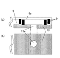
図32において、表示素子・撮像素子モジュールとしての受光素子一体型液晶ディスプレイモジュール51は、ディスプレイ(表示装置)としての液晶ディスプレイ52の一部を構成する透光性支持基板53に、外部配線用の電極部としての電極パッド54を有する電子素子としての受光素子チップ55が搭載されている。この受光素子チップ55の各電極パッド54と、ガラス基板などの透光性支持基板53のランド部56aとを導電突起57を用いて電気的に接続している。透光性支持基板53と受光素子チップ55との接続部は、樹脂粒子の表面を導電膜、例えば金でコーティングした導電粒子58を介在させた状態で接着用の樹脂59で固め、この受光領域60の配置範囲を避けるようにして樹脂59が配設されている。受光素子チップ55の反対側の透光性支持基板53(裏面)には、受光素子チップ55の素子領域としての受光領域60(撮像領域)に入射光を集光させるためのレンズユニット61が設けられている。このレンズユニット61は、一または複数のレンズが遮光ホルダで保持された状態で光入射口以外の周りが遮光されている。   In FIG. 32, a light receiving element integrated liquid crystal display module 51 as a display element / imaging element module is provided on a translucent support substrate 53 constituting a part of a liquid crystal display 52 as a display (display device). A light receiving element chip 55 as an electronic element having an electrode pad 54 as an electrode portion is mounted. The electrode pads 54 of the light receiving element chip 55 are electrically connected to the land portions 56 a of the translucent support substrate 53 such as a glass substrate using conductive protrusions 57. The connection part between the translucent support substrate 53 and the light receiving element chip 55 is solidified with an adhesive resin 59 with conductive particles 58 coated with a conductive film, for example, gold, on the surface of the resin particles. The resin 59 is arranged so as to avoid the arrangement range of 60. A lens unit 61 for condensing incident light on a light receiving region 60 (imaging region) as an element region of the light receiving element chip 55 is provided on the translucent support substrate 53 (back surface) opposite to the light receiving element chip 55. It has been. The lens unit 61 is shielded from light other than the light entrance with one or more lenses held by the light-shielding holder.

これらの透光性支持基板53の表面側に受光素子チップ55が樹脂59などの接着材で固定され、透光性支持基板53の裏面側に、受光素子チップ55の受光領域60に入射光を集光させるようにレンズユニット61が固定されて撮像モジュール20Dが構成されている。   The light receiving element chip 55 is fixed to the front surface side of the translucent support substrate 53 with an adhesive such as a resin 59, and incident light is incident on the light receiving region 60 of the light receiving element chip 55 on the back surface side of the translucent support substrate 53. The lens unit 61 is fixed so as to collect light, and the imaging module 20D is configured.

一方、液晶ディスプレイ52は、2枚の透光性支持基板53および62を上下に重ね合わせ、これらの間に液晶材料63を封入して構成されている。透光性支持基板53および62としては、透明な種々のガラス材料や樹脂材料が用いられる。透光性支持基板53の一方面(上面)には基板配線が設けられ、この基板配線のランド部56aを除く配線部56bと少なくともその近傍位置が、保護膜としての絶縁膜64により覆われている。この絶縁膜64は、外部環境から基板配線のランド部56a周辺やそれ以外の配線部56bを化学的、物理的ダメージから保護している。   On the other hand, the liquid crystal display 52 is configured by superimposing two translucent support substrates 53 and 62 on top and bottom and enclosing a liquid crystal material 63 therebetween. As the translucent support substrates 53 and 62, various transparent glass materials and resin materials are used. A substrate wiring is provided on one surface (upper surface) of the translucent support substrate 53, and the wiring portion 56b excluding the land portion 56a of this substrate wiring and at least the vicinity thereof are covered with an insulating film 64 as a protective film. Yes. The insulating film 64 protects the periphery of the land portion 56a of the substrate wiring and other wiring portions 56b from chemical and physical damage from the external environment.

液晶ディスプレイ52の基板配線材料としては、アルミニュウム、タンタル、タンタルナイトライド、ニッケル、モリブデン、銅、金、白金、タングステン、チタンおよびITOなどの各種の材料膜が用いられる。この基板配線は、これらの材料の中から単層または複数層で用いられる。この基板配線材料は、必要に応じて、これらの中から選ばれ、使用箇所によって使い分けされる。本実施形態3では、液晶ディスプレイ52において、アルミニュウム、タンタルナイトライド、チタンおよびITOのいずれかを用い、受光素子チップ55の搭載領域に引き回す基板配線も、この中の全てまたはその一部の材料を用いることにより、液晶ディスプレイ52の場合と同様のプロセスで、受光素子チップ55の搭載領域への基板配線も製造可能となり、製造工程を複雑化しないで済む。   As a substrate wiring material of the liquid crystal display 52, various material films such as aluminum, tantalum, tantalum nitride, nickel, molybdenum, copper, gold, platinum, tungsten, titanium, and ITO are used. The substrate wiring is used in a single layer or a plurality of layers from these materials. This substrate wiring material is selected from these as required, and is properly used depending on the place of use. In the third embodiment, the liquid crystal display 52 uses any one of aluminum, tantalum nitride, titanium, and ITO, and the substrate wiring routed to the mounting region of the light receiving element chip 55 is made of all or part of the material. By using it, it is possible to manufacture substrate wiring to the mounting region of the light receiving element chip 55 in the same process as the case of the liquid crystal display 52, and the manufacturing process does not have to be complicated.

なお、一般的な液晶ディスプレイモジュールとしては、受光素子チップの搭載基板として、液晶ディスプレイの一部を構成する透光性支持基板とは別に基板を設け、液晶ディスプレイ用の透光性支持基板と受光素子チップの搭載基板とを互いに接続して用いられる。これに対して、本実施形態3では、液晶ディスプレイ52の一部を構成する透光性支持基板53に直接、受光素子チップ55が搭載されるため、別途、受光素子チップ55の搭載基板を準備する必要がなく、基板間を接続する手間も省かれる。また、透光性支持基板53に直接、受光素子チップ55を搭載するため、受光素子一体型液晶ディスプレイモジュール51を小型化することも可能となる。   In addition, as a general liquid crystal display module, a substrate is provided as a substrate for mounting a light receiving element chip, in addition to a light transmissive support substrate that constitutes a part of the liquid crystal display. The element chip mounting substrate is connected to each other. On the other hand, in the third embodiment, since the light receiving element chip 55 is directly mounted on the translucent support substrate 53 constituting a part of the liquid crystal display 52, a mounting substrate for the light receiving element chip 55 is separately prepared. This eliminates the need to connect the substrates. Since the light receiving element chip 55 is directly mounted on the translucent support substrate 53, the light receiving element integrated liquid crystal display module 51 can be downsized.

受光素子チップ55の中央部分には、入射光を光電変換して撮像する複数の受光部が設けられた受光領域60が形成されており、この受光領域60の光入射面側には、集光能力を高める目的で微小レンズ65(マイクロレンズ)が設けられている。これは画素数の多いタイプの固体撮像素子(受光素子チップ55)においては、一つの画素が小さいため、画素当たりの集光能力が低くなるためである。微小レンズ65は、スチレン系またはアクリル系樹脂、シリコン窒化膜、シリコン酸化膜などの材料かまたは、これらが複数層で設けられる。受光領域60を取り囲む受光領域60の周辺領域(以降、受光周辺領域という)に電極部としての電極パッド54を有する。この電極パッド54は、例えば平面視4角形の形状である受光素子チップ55の4辺または4辺のうちの少なくとも1辺に存在する。1辺に存在する場合は、対向する辺などにスペーサを形成するとよい。このスペーサとしては、導電突起でもよいし非導電突起でもよい。電極パッド54は一般的にはアルミニュウム系または銅系の金属材料が用いられる。
受光素子チップ55の場合は表面の汚染を避けるために、電極パッド54上に設けられる導電突起57として、金属細線から形成するワイヤバンプを用いるとよい。金属細線としては金が一般的に用いられるが、他にアルミニュウムや銅などでもよい。本実施形態3では、この中で酸化の影響を受けにくく、形状が安定する金からなるワイヤバンプを用いている。電極パッド54が銅系の金属の場合は、最表面にアルミニュウム系の金属を設けることで対応できる。導電突起57はチップ個片状態で設けても良いし、チップ状態に個片化する前のウエハ状態で設けてもよい。製造上は後者の方が量産性に優れている。
電極パッド54に導電突起57を設けた受光素子チップ55は、基板配線(ランド部56aおよびそれ以外の配線部56b)が施された透光性支持基板53のランド部56aに、上記導電突起57が各々位置合わせされて搭載される。これらの電気的接続は、導電突起57とランド56aを直接接続してもよいし、導電突起57とランド56a間において、導電粒子58を介在させてもよい。このとき、上記接続方法によらず、受光素子チップ55の接続部は、樹脂59で固めることにより、受光素子チップ55と透光性支持基板53との接続部を保護することができる。導電粒子58を介して電気的に接合する場合は、ワイヤバンプの頂部をあらかじめ平坦化しておくと、導電粒子58の介在数が多くできるのでよい。その頂部のサイズは40μmから80μm程度とすると導電粒子58の介在数を確保できる。導電粒子58を含有する樹脂材料には、その例として異方性導電樹脂材料(導電させたい例えば加圧した縦方向のみ導電し、加圧しない横方向には導電しない導電接着材)であるACF(フィルム)やACP(ペイスト)がある。一方、導電粒子58を含まない樹脂材料には、その例としてNCP、アンダーフィル材などがある。これらACF、ACP、NCP、アンダーフィル材などの樹脂材料は非導電粒子を含有することができる。非導電粒子には、シリカやアルミナなどがある。これらの非導電粒子は、樹脂材料が一般的に、熱膨張係数が高いため、導電突起、ガラスやICチップなどに熱膨張係数を近づけるのに有効である。NCPやアンダーフィル材で受光素子チップ55の接続部を固める場合においては、導電突起57の頂部が尖った形状としておく方がよい。受光素子チップ55の接続の前に予め樹脂を塗布するNCPを用いる方法では、接続面へのNCP材料の巻き込みを防止できる。また、受光素子チップ55が導電突起57を介して接続された後に、樹脂59を注入して接続部を固める方法においても、頂部が尖った先端形状としておく方が、ボンディング圧力を小さく設定できるため、受光素子チップ55へのダメージを低減できる。特に、受光素子チップ55の厚さが0.3mm以下の場合に、受光素子チップ55の強度が弱くなるので有効である。いずれの樹脂59を用いる場合においても、受光素子チップ55の少なくとも接続部を固め、受光領域60の位置を避けるようにして形成することが重要である。このためには、樹脂59の量を調節して塗布(ACP(導電粒子があるタイプ)、NCP(導電粒子がないタイプ))、貼り付け(ACF)、注入(アンダーフィル材)などの作業を行う。
In the central portion of the light receiving element chip 55, a light receiving region 60 provided with a plurality of light receiving portions for photoelectrically converting incident light to form an image is formed. A micro lens 65 (micro lens) is provided for the purpose of enhancing the capability. This is because in a solid-state imaging device (light-receiving element chip 55) of a type having a large number of pixels, since one pixel is small, the light condensing capability per pixel is low. The micro lens 65 is made of a material such as a styrene resin or an acrylic resin, a silicon nitride film, a silicon oxide film, or a plurality of layers. An electrode pad 54 as an electrode portion is provided in a peripheral region of the light receiving region 60 surrounding the light receiving region 60 (hereinafter referred to as a light receiving peripheral region). The electrode pad 54 is present on at least one side of four sides or four sides of the light receiving element chip 55 having, for example, a quadrangular shape in plan view. In the case of being on one side, a spacer may be formed on the opposite side or the like. The spacer may be a conductive protrusion or a nonconductive protrusion. The electrode pad 54 is generally made of an aluminum-based or copper-based metal material.
In the case of the light receiving element chip 55, in order to avoid contamination of the surface, it is preferable to use wire bumps formed from fine metal wires as the conductive protrusions 57 provided on the electrode pads 54. Gold is generally used as the thin metal wire, but aluminum or copper may also be used. In the third embodiment, wire bumps made of gold that are not easily affected by oxidation and have a stable shape are used. When the electrode pad 54 is made of a copper-based metal, it can be dealt with by providing an aluminum-based metal on the outermost surface. The conductive protrusions 57 may be provided in a chip individual state or may be provided in a wafer state before being separated into chip states. In terms of production, the latter is superior in mass productivity.
The light receiving element chip 55 provided with the conductive protrusions 57 on the electrode pads 54 has the conductive protrusions 57 on the land portions 56a of the translucent support substrate 53 on which the substrate wiring (land portions 56a and other wiring portions 56b) is applied. Are aligned and mounted. For these electrical connections, the conductive protrusions 57 and the lands 56a may be directly connected, or the conductive particles 58 may be interposed between the conductive protrusions 57 and the lands 56a. At this time, regardless of the connection method, the connection portion between the light receiving element chip 55 and the translucent support substrate 53 can be protected by hardening the connection portion of the light receiving element chip 55 with the resin 59. When electrical bonding is performed through the conductive particles 58, the number of intervening conductive particles 58 can be increased by planarizing the top of the wire bumps in advance. If the size of the top portion is about 40 μm to 80 μm, the number of interposed conductive particles 58 can be secured. For example, the resin material containing the conductive particles 58 is an ACF which is an anisotropic conductive resin material (for example, a conductive adhesive that is conductive only in the pressurized vertical direction and is not conductive in the horizontal direction that is not pressurized). (Film) and ACP (paste). On the other hand, examples of the resin material that does not include the conductive particles 58 include NCP and an underfill material. These resin materials such as ACF, ACP, NCP, and underfill material can contain non-conductive particles. Non-conductive particles include silica and alumina. Since these non-conductive particles generally have a high thermal expansion coefficient, they are effective in bringing the thermal expansion coefficient closer to conductive protrusions, glass, IC chips, and the like. In the case where the connection portion of the light receiving element chip 55 is hardened with NCP or an underfill material, it is preferable that the top portion of the conductive protrusion 57 has a sharp shape. In the method using NCP in which a resin is applied in advance before connection of the light receiving element chip 55, it is possible to prevent the NCP material from being caught on the connection surface. Also, in the method of injecting the resin 59 after the light receiving element chip 55 is connected via the conductive protrusion 57 and solidifying the connecting portion, the tip shape with a sharp top can set the bonding pressure smaller. The damage to the light receiving element chip 55 can be reduced. In particular, when the thickness of the light receiving element chip 55 is 0.3 mm or less, the strength of the light receiving element chip 55 becomes weak, which is effective. In the case of using any of the resins 59, it is important that at least the connection portion of the light receiving element chip 55 is hardened so as to avoid the position of the light receiving region 60. For this purpose, operations such as coating (ACP (type with conductive particles), NCP (type without conductive particles)), pasting (ACF), injection (underfill material), etc., by adjusting the amount of resin 59 are performed. Do.

図32では、導電粒子58を含有する透明樹脂材料であるACPまたはACFを用いた例である。ACPの場合、導電粒子58は、その直径が2μm〜7μmを平均値とするとよい。さらには、2μm〜4μm程度とした方が含有比率をそのままで導電粒子58の数を増やすことができるので、一端子当たりの導電粒子58の介在数を増やすことができる。そのため、より確実に電気的接続ができる。これが極端に小さいと、技術的、コスト的に困難になってくる。含有比率は7〜18wtパーセント程度が良い。このことで、一端子当たりの導電粒子58が介在しない確率を減らし、隣り合う端子間でのショートを減らすことができる。非導電粒子を含有させると、熱膨張係数の差による、透光性支持基板53と樹脂59の接合面、または受光素子チップ55と樹脂59の接合面の剥離を抑制することができる。非導電粒子は、導電粒子58よりも小さな径のものを含有させて、導電粒子58による電気的接続を阻害しないようにする必要がある。例えば、非導電粒子径は、導電粒子径の30〜80パーセント程度とするとよい。即ち、導電粒子58の径が5μmのとき、非導電粒子の径は1.5μm〜4μm程度、導電粒子58の径が3μmのとき、非導電粒子の平均径は1μm〜2.4μm程度とするとよい。非導電粒子の含有比率は作業性を考慮した上で、できるだけ含有させた方が熱膨張係数を下げることができるためよい。これらのACP、NCP、アンダーフィル材においては20〜70wtパーセント程度がよい。   FIG. 32 shows an example using ACP or ACF, which is a transparent resin material containing conductive particles 58. In the case of ACP, the conductive particles 58 may have an average value of 2 μm to 7 μm in diameter. Furthermore, since it is possible to increase the number of conductive particles 58 while keeping the content ratio as it is, the number of conductive particles 58 per terminal can be increased when the content ratio is about 2 μm to 4 μm. Therefore, electrical connection can be made more reliably. If this is extremely small, it becomes difficult in terms of technology and cost. The content ratio is preferably about 7 to 18 wt percent. As a result, the probability that the conductive particles 58 per terminal do not intervene can be reduced, and a short circuit between adjacent terminals can be reduced. When non-conductive particles are contained, peeling of the bonding surface between the translucent support substrate 53 and the resin 59 or the bonding surface between the light receiving element chip 55 and the resin 59 due to a difference in thermal expansion coefficient can be suppressed. The non-conductive particles need to contain particles having a diameter smaller than that of the conductive particles 58 so that the electrical connection by the conductive particles 58 is not hindered. For example, the non-conductive particle diameter may be about 30 to 80 percent of the conductive particle diameter. That is, when the diameter of the conductive particles 58 is 5 μm, the diameter of the nonconductive particles is about 1.5 μm to 4 μm, and when the diameter of the conductive particles 58 is 3 μm, the average diameter of the nonconductive particles is about 1 μm to 2.4 μm. Good. The content ratio of the non-conductive particles is good because the thermal expansion coefficient can be lowered when it is contained as much as possible in consideration of workability. In these ACPs, NCPs, and underfill materials, about 20 to 70 wt percent is preferable.

図33は、本発明の実施形態3に係る受光素子一体型液晶ディスプレイモジュールの他の構成例を示す要部断面図である。   FIG. 33 is a cross-sectional view of a main part showing another configuration example of the light receiving element-integrated liquid crystal display module according to Embodiment 3 of the present invention.

図33では、受光素子一体型液晶ディスプレイモジュール51として、透光性支持基板3における受光素子チップ4の受光周辺領域に重なる領域に段差部71を設けている点が図33の場合と異なっている。   33 is different from the case of FIG. 33 in that the light receiving element integrated liquid crystal display module 51 is provided with a stepped portion 71 in a region overlapping the light receiving peripheral region of the light receiving element chip 4 in the translucent support substrate 3. .

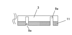
この段差部71は、少なくとも受光素子チップ55の接続部の少なくとも内側の領域に設けると、樹脂59の受光領域60への形成(広がり)を防ぐのでよい。例えば、受光素子チップ55における接続部が受光素子チップ55の平面視矩形または正方形の1辺に沿ってある場合は、その1辺と受光領域60との間に段差部71を設けるとよい。これと同様に、その接続部が受光素子チップ55の平面視矩形または正方形の2辺に存在する場合には、その2辺と受光領域60との間に段差部71を設け、接続部が3辺にある場合は、その3辺と受光領域60との間に段差部71(堰止め部;ダム部)を設け、接続部が4辺にある場合には、その4辺と受光領域60との間に段差部71を設けるとよい。ただし、各接続部の辺の数に関わらず、受光領域60を囲むように、4角形などの多角形や円形などのように全体的に略繋るように形成すると、より確実に樹脂59の受光領域60側への流れ込みを防止することができる。   If the stepped portion 71 is provided at least in the region inside the connection portion of the light receiving element chip 55, the formation (spreading) of the resin 59 in the light receiving region 60 may be prevented. For example, when the connection portion in the light receiving element chip 55 is along one side of the light receiving element chip 55 in a rectangular or square shape in plan view, a stepped portion 71 may be provided between the one side and the light receiving region 60. Similarly, when the connection portion exists on two sides of the rectangular or square in plan view of the light receiving element chip 55, a step portion 71 is provided between the two sides and the light receiving region 60, and the connection portion is 3 In the case of being on the side, a stepped portion 71 (damming portion; dam portion) is provided between the three sides and the light receiving region 60, and when the connecting portion is on the four sides, the four sides and the light receiving region 60 A stepped portion 71 may be provided between the two. However, regardless of the number of sides of each connecting portion, if the resin 59 is formed so as to be generally connected like a polygon such as a quadrangle or a circle so as to surround the light receiving region 60, the resin 59 can be more reliably connected. Inflow to the light receiving region 60 side can be prevented.

この段差部71を設けるには、紫外線などの電磁波を照射することによって硬化する材料や、低温速硬化が可能な樹脂を描画法、印刷法、インクジェット法などを用いて設けるとよい。電磁波またはホットプレートによる硬化では、局部的な照射、加熱を行うことができるので、液晶ディスプレイ52のダメージを防ぐことができる。この段差部71の代わりに、受光領域60に対向する透光性支持基板53上の所定領域に、樹脂59をはじく性質を有する材料膜を設けてもよい。さらに、この段差部71の少なくとも側面または表面、もしくは側面と表面に樹脂59をはじく性質を持たせてもよく、これを実現するために、フッ素系ガスを用いたプラズマ処理を施すか、樹脂59をはじく性質の材料膜で覆ってもよい。プラズマ処理を行う場合には段差がなくてもよい。また、段差部71そのものが樹脂59をはじく材料であってもよい。テフロン(登録商標)樹脂やITO材料は、エポキシ系樹脂などの樹脂59をはじく性質を持つ。特にITO材料は、液晶ディスプレイ52の透明電極としても用いるため、透光性支持基板53に形成する場合には、液晶ディスプレイ52の製造プロセスと共通であるため、製造上の複雑化を避けることができるため更によい。   In order to provide the stepped portion 71, a material that can be cured by irradiating electromagnetic waves such as ultraviolet rays or a resin that can be cured at low temperature and high speed may be provided using a drawing method, a printing method, an inkjet method, or the like. In the curing by the electromagnetic wave or the hot plate, since the local irradiation and heating can be performed, the liquid crystal display 52 can be prevented from being damaged. Instead of the stepped portion 71, a material film having a property of repelling the resin 59 may be provided in a predetermined region on the translucent support substrate 53 facing the light receiving region 60. Furthermore, at least the side surface or the surface of the stepped portion 71 or the side surface and the surface may have a property of repelling the resin 59. In order to realize this, plasma treatment using a fluorine-based gas is performed, or the resin 59 is repelled. It may be covered with a material film having a property of repelling. In the case of performing plasma treatment, there is no need for a step. Further, the stepped portion 71 itself may be a material that repels the resin 59. Teflon (registered trademark) resin and ITO material have a property of repelling resin 59 such as epoxy resin. In particular, since the ITO material is also used as a transparent electrode of the liquid crystal display 52, when it is formed on the translucent support substrate 53, it is common with the manufacturing process of the liquid crystal display 52, so that the manufacturing complexity is avoided. It is even better because it can.

これらの段差部71または樹脂59をはじく材料、もしくは樹脂59をはじく表面処理の他に、図35のように、樹脂59をはじく段差部72を、透光性支持基板53における受光素子チップ55と重なる領域の外周部(外側)に設けてもよく、このことにより、受光素子チップ55の外周部における樹脂59の更に外周部への広がりを抑制することができる。このため、液晶ディスプレイ52などの他の部品にまで樹脂59が流れ込むことを防ぐことができる。この樹脂59をはじく段差部72は、少なくとも樹脂59の流れ込みを避けるべき部品との間に設けるとよい。受光素子チップ55の周辺全体に囲むように、受光素子チップ55の矩形または正方形状と略相似形状で全体が略繋がった形状にすると、受光素子チップ55の外周への樹脂59の広がりをより確実に制限することができるのでさらによい。   In addition to the material that repels the stepped portion 71 or the resin 59, or the surface treatment that repels the resin 59, the stepped portion 72 that repels the resin 59 is connected to the light receiving element chip 55 on the translucent support substrate 53 as shown in FIG. You may provide in the outer peripheral part (outer side) of the overlapping area | region, and, thereby, the spreading | diffusion to the outer peripheral part of the resin 59 in the outer peripheral part of the light receiving element chip | tip 55 can be suppressed. For this reason, the resin 59 can be prevented from flowing into other parts such as the liquid crystal display 52. The stepped portion 72 that repels the resin 59 is preferably provided at least between the parts where the flow of the resin 59 should be avoided. If the shape is substantially similar to the rectangular or square shape of the light receiving element chip 55 so as to surround the entire periphery of the light receiving element chip 55, the resin 59 spreads more reliably to the outer periphery of the light receiving element chip 55. This is even better.

次に、これらの段差部71および/または段差部72、これらの代わりにまたはこれらと共に、樹脂59をはじく材料または樹脂59をはじく表面処理は、図34、図36および図37のように、透光性樹脂基板53側に限らず、受光素子チップ55側にあってもよく、透光性樹脂基板53と受光素子チップ55の両方であると更によい。   Next, the stepped portion 71 and / or the stepped portion 72, instead of or in combination with these, the material that repels the resin 59 or the surface treatment that repels the resin 59 is transparent as shown in FIGS. 34, 36, and 37. Not only the light-sensitive resin substrate 53 side but also the light-receiving element chip 55 side, or both the light-transmitting resin substrate 53 and the light-receiving element chip 55 are better.

このように、段差部71、72が受光素子チップ55側にある場合については、以下のような効果がある。   As described above, when the stepped portions 71 and 72 are on the light receiving element chip 55 side, the following effects are obtained.

受光領域60の周囲の受光周辺領域の段差部71、この代わりにまたはこれと共に、樹脂59をはじく材料または樹脂59をはじく表面処理は、受光領域60への直接的に樹脂59の流入を防ぐことができる。また、受光素子チップ55の周辺の段差部72、この代わりにまたはこれと共に、樹脂59をはじく材料または樹脂59をはじく表面処理は、ACP、NCPやACF材料のボンディング時のボンディングツールへの樹脂59の付着を防止することが可能である。特に、ペースト状であり塗布形状や塗布量にバラツキが生じやすいACP、NCPについては有効である。受光素子チップ55側への段差部71、72、これらの代わりにまたはこれらと共に、樹脂59をはじく材料または樹脂59をはじく表面処理は、紫外線などの電磁波を照射することによって硬化する樹脂材料や、低温速硬化が可能な樹脂材料を、描画法、印刷法、インクジェット法などを用いて塗布するとよい。また、フッ素系ガスによるプラズマ処理でもよい。透光性支持基板53または受光素子チップ55へのプラズマ処理を行う場合は、感光性レジストなどでパターニングしてマスクにすると、所望の領域において、樹脂59をはじく領域を容易かつ確実に形成することができる。   The step portion 71 of the light receiving peripheral region around the light receiving region 60, or instead of or together with this, the material that repels the resin 59 or the surface treatment that repels the resin 59 prevents the inflow of the resin 59 directly into the light receiving region 60. Can do. Further, the stepped portion 72 around the light receiving element chip 55, or instead of or together with this, the material that repels the resin 59 or the surface treatment that repels the resin 59 is a resin 59 to the bonding tool when bonding ACP, NCP, or ACF material. Can be prevented. In particular, it is effective for ACP and NCP that are paste-like and tend to vary in the application shape and application amount. Step portions 71 and 72 toward the light receiving element chip 55, instead of or together with these, a material that repels the resin 59 or a surface treatment that repels the resin 59 is a resin material that is cured by irradiating electromagnetic waves such as ultraviolet rays, A resin material that can be cured at low temperature and high speed may be applied using a drawing method, a printing method, an inkjet method, or the like. Further, plasma treatment with a fluorine-based gas may be used. When plasma processing is performed on the translucent support substrate 53 or the light receiving element chip 55, if a mask is formed by patterning with a photosensitive resist or the like, a region that repels the resin 59 can be easily and reliably formed in a desired region. Can do.

アクリル系などの樹脂を用いた微小レンズ65を有する受光素子チップ55では、微小レンズ65の熱による劣化、または反射防止膜を更に設ける場合は、反射防止膜のクラックを防ぐために、できるだけ高温とならないような摂氏220度以下での熱処理が必要である。また、受光素子チップ55の製造プロセスと共通にすると製造上の複雑化を防ぐことができる。例えばアクリル系の樹脂、シリコン酸化膜、シリコン窒化膜などのカバー膜66などを用いるとよい。特に、アクリル系樹脂からなる微小レンズ65の形成と同時に受光周辺領域および/または受光素子チップ55の周辺領域に段差部71を設けると、厚さを厚くできるのでよい。また、その段差部71、72の表面にシリコン酸化膜、シリコン窒化膜からなる表面保護膜などを追加で形成してもよい。   In the light receiving element chip 55 having the microlens 65 using an acrylic resin or the like, when the microlens 65 is deteriorated by heat or an antireflection film is further provided, the temperature is not as high as possible in order to prevent the antireflection film from cracking. Such heat treatment at 220 degrees centigrade or lower is necessary. Further, if the manufacturing process of the light receiving element chip 55 is made common, the manufacturing complexity can be prevented. For example, a cover film 66 such as an acrylic resin, a silicon oxide film, or a silicon nitride film may be used. In particular, if the stepped portion 71 is provided in the light receiving peripheral region and / or the peripheral region of the light receiving element chip 55 simultaneously with the formation of the microlens 65 made of acrylic resin, the thickness may be increased. Further, a surface protective film made of a silicon oxide film or a silicon nitride film may be additionally formed on the surface of the stepped portions 71 and 72.

図38は、本発明の実施形態3に係る受光素子一体型液晶ディスプレイモジュールの更に他の構成例を示す要部断面図である。   FIG. 38 is a cross-sectional view of the main part showing still another configuration example of the light receiving element-integrated liquid crystal display module according to Embodiment 3 of the present invention.

図38では、受光素子チップ55の少なくとも接続部をACP樹脂である樹脂59で固めており、さらにその樹脂59の周辺を別の樹脂59Aで固めている。この別の樹脂59Aにより、受光素子チップ55を固定することができるため、携帯電話装置などで求められる落下衝撃などに対して、さらに強くなる。また、確実に、透光性支持基板53と受光素子チップ55の中央部分との間を気密にすることができるので、外部からの異物の浸入や水分の浸入を防ぐことができる。この別の樹脂59Aは、樹脂59と同様に導電性粒子58を含有する同じ樹脂材料であると、熱膨張率が同じであるため、樹脂59A、59の界面での剥離を防止できる。ただし、この場合には、コスト高になるので、シリカなどの非導電粒子のみを含有させるとよい。別の樹脂59Aにおける非導電粒子の含有量を、樹脂59における非導電粒子の含有量と同じ程度含有させるとよい。さらには、導電粒子58を含有する樹脂59と、別の樹脂59Aが略同じ熱膨張係数となるように、別の樹脂59Aの非導電粒子の含有率を調節するとよい。樹脂59別の樹脂59Aまたは、別の樹脂59Aと樹脂59は遮光性の物質を含有していると、受光素子チップ55の側面からの光の浸入を防ぐことができる。   In FIG. 38, at least the connection portion of the light receiving element chip 55 is solidified with a resin 59 which is an ACP resin, and the periphery of the resin 59 is solidified with another resin 59A. Since the light receiving element chip 55 can be fixed by the other resin 59A, the resin 59A is more resistant to a drop impact required for a mobile phone device or the like. Further, since the space between the translucent support substrate 53 and the center portion of the light receiving element chip 55 can be surely sealed, it is possible to prevent the entry of foreign matter and moisture from the outside. If the other resin 59A is the same resin material containing the conductive particles 58 as the resin 59, the thermal expansion coefficient is the same, and therefore, peeling at the interface between the resins 59A and 59 can be prevented. However, in this case, since the cost is high, it is preferable to include only non-conductive particles such as silica. The content of non-conductive particles in another resin 59A may be included to the same extent as the content of non-conductive particles in resin 59. Furthermore, the content ratio of the non-conductive particles of the other resin 59A may be adjusted so that the resin 59 containing the conductive particles 58 and the other resin 59A have substantially the same thermal expansion coefficient. When the resin 59A or the resin 59A and the resin 59 contain a light-shielding substance, it is possible to prevent light from entering from the side surface of the light receiving element chip 55.

図39は、本発明の実施形態3に係る受光素子一体型液晶ディスプレイモジュールの更に他の構成例を示す要部断面図である。   FIG. 39 is a cross-sectional view of the main part showing still another configuration example of the light receiving element-integrated liquid crystal display module according to Embodiment 3 of the present invention.

図39では、受光素子チップ55の裏面上を封止樹脂59Bで覆っており、この例では、受光素子チップ55の側面と裏面上に一体的に同じ樹脂材料で封止している点が他の構成例のものと異なっている。この封止樹脂59Bにおいても、樹脂59Aの場合と同様に、非導電粒子の含有量を、樹脂59における非導電粒子の含有量と同じ程度含有させるとよい。さらには、導電粒子58を含有する樹脂59と、封止樹脂59Bが略同じ熱膨張係数となるように樹脂59Aの非導電粒子の含有率を調節するとよい。樹脂59、封止樹脂59Bまたは、樹脂59と樹脂59Bが遮光性の物質を含有していると、さらに受光領域60に光が入らないのでよい。このことで、図38の構成における効果に加えて、外部からの物理的、化学的ダメージからの保護効果が向上し、受光素子チップ55の裏面からの光の浸入をより確実に防ぐことができる。特にチップ厚が薄い場合に有効である。   In FIG. 39, the back surface of the light receiving element chip 55 is covered with a sealing resin 59B. In this example, the other side is that the side surface and the back surface of the light receiving element chip 55 are integrally sealed with the same resin material. This is different from the configuration example. Also in the sealing resin 59B, the content of the non-conductive particles may be included to the same extent as the content of the non-conductive particles in the resin 59, as in the case of the resin 59A. Furthermore, the content ratio of the non-conductive particles of the resin 59A may be adjusted so that the resin 59 containing the conductive particles 58 and the sealing resin 59B have substantially the same thermal expansion coefficient. If the resin 59, the sealing resin 59B, or the resin 59 and the resin 59B contain a light-shielding substance, light may not enter the light receiving region 60. Thus, in addition to the effects in the configuration of FIG. 38, the protection effect from physical and chemical damage from the outside is improved, and the intrusion of light from the back surface of the light receiving element chip 55 can be more reliably prevented. . This is particularly effective when the chip thickness is thin.

図40は、本発明の実施形態3に係る受光素子一体型液晶ディスプレイモジュールの更に他の構成例を示す要部断面図である。   FIG. 40 is a cross-sectional view of relevant parts showing still another configuration example of the light receiving element-integrated liquid crystal display module according to Embodiment 3 of the present invention.

図40では、図35において樹脂59が導電粒子58を用いた異方性導電樹脂材料のACFまたはACPを用いたことに対して、樹脂59Cは、導電粒子58を用いないNCPまたはアンダーフィル材料を用いた点が他の例のものと異なっている。   In FIG. 40, in FIG. 35, the resin 59 uses the anisotropic conductive resin material ACF or ACP using the conductive particles 58, whereas the resin 59C uses an NCP or underfill material that does not use the conductive particles 58. The point used is different from the other examples.

アンダーフィル材料を用いる場合は、導電突起57と、基板配線のランド部56a上の導電突起57Aとを直接接合する。導電突起57としては例えば金からなるワイヤバンプを形成し、ランド部56a上の導電突起57Aとしては例えばインジウム合金を形成しこれらを接続する。この接続後、アンダーフィル材料を注入するのである。この場合においても、透光性支持基板53上において、受光素子チップ55の受光周辺領域と重なる領域と、受光素子チップ55の周辺に、段差部71,72(堰止め部;ダム部)および/または、樹脂59Cをはじく材料または樹脂59Cをはじく表面処理を行っている。   When an underfill material is used, the conductive protrusion 57 and the conductive protrusion 57A on the land portion 56a of the substrate wiring are directly bonded. For example, a wire bump made of gold is formed as the conductive protrusion 57, and an indium alloy is formed as the conductive protrusion 57A on the land portion 56a, and these are connected. After this connection, an underfill material is injected. Also in this case, on the translucent support substrate 53, the stepped portions 71 and 72 (damping portion; dam portion) and / or the region overlapping the light receiving peripheral region of the light receiving element chip 55 and the periphery of the light receiving element chip 55 are provided. Alternatively, a material that repels the resin 59C or a surface treatment that repels the resin 59C is performed.

したがって、この段差部71,72および/または、樹脂59Cをはじく材料または樹脂59Cをはじく表面処理によって、アンダーフィル材料は受光領域60への流入を防ぎ、受光素子チップ55の外周部において流れ出しを防いでいる。NCPを用いる場合は、予め透光性支持基板53に、NCPを描画、印刷などで施しておき、受光素子チップ55に導電突起57,57Aを介して熱圧着し、それを加圧したまま接続部を樹脂59Cで固める。この場合も、段差部71,72および/または、樹脂59Cをはじく材料または樹脂59Cをはじく表面処理によって、樹脂59Cは受光領域60への流入が防がれ、受光素子チップ55の外周部において樹脂59Cの流れ出しを防いでいる。NCPを用いる場合、導電突起57Aはなくてもよい。   Therefore, the stepped portions 71 and 72 and / or the material that repels the resin 59C or the surface treatment that repels the resin 59C prevents the underfill material from flowing into the light receiving region 60, and prevents the underfill material from flowing out at the outer peripheral portion of the light receiving element chip 55. It is out. When NCP is used, the NCP is drawn on the translucent support substrate 53 in advance by drawing, printing, etc., and thermally bonded to the light receiving element chip 55 via the conductive protrusions 57 and 57A, and connected while being pressurized. The part is hardened with resin 59C. Also in this case, the stepped portions 71 and 72 and / or the material that repels the resin 59C or the surface treatment that repels the resin 59C prevents the resin 59C from flowing into the light receiving region 60, and the resin is formed at the outer peripheral portion of the light receiving element chip 55. 59C is prevented from flowing out. When NCP is used, the conductive protrusion 57A may not be provided.

図41は、本発明の実施形態3に係る受光素子一体型液晶ディスプレイモジュールの更に他の構成例を示す要部断面図である。   FIG. 41 is a cross-sectional view of a main part showing still another configuration example of the light receiving element-integrated liquid crystal display module according to Embodiment 3 of the present invention.

図41では、透光性支持基板53Aとして両面配線が施されている点が他の例と異なっている。両面配線間には透光性支持基板53Aを貫通孔を介して貫通する配線が施されるかまたは、透光性支持基板53の側面に配線を設けて両面の配線間を電気的に接続してもよい。両面配線が施された透光性支持基板53Aを用いることによって、図32〜図40の場合とは異なり、透光性支持基盤53の反対面側に受光素子チップ55を導電突起57を介して接続できる。なお、段差部71および/または、樹脂59をはじく材料または樹脂59をはじく表面処理は、種々の組み合わせの位置、材料、処理を組み合わせることができる。例えば図40の例において、受光素子チップ55上に設けてもよい。また、図32〜図41には、レンズユニット61が設けられている。さらに、透光性支持基板53上には、駆動用半導体素子などが設けられているとさらにコンパクトになる。受光素子チップ55は複数個搭載されていてもよく、透光性支持基板53の反対面同士に搭載されているとアウトカメラ、インカメラとして使えることも想定される。また、反対面同士に受光素子チップ55を設けなくても、一方の面に2個設けても、受光素子チップ55の向きによってアウトカメラ、インカメラとして使うことができる。   41 is different from the other examples in that double-sided wiring is provided as the translucent support substrate 53A. Between the double-sided wirings, wiring that penetrates the translucent support substrate 53A through a through hole is provided, or wiring is provided on the side surface of the translucent support substrate 53 to electrically connect the wirings on both sides. May be. By using the translucent support substrate 53A provided with the double-sided wiring, unlike the case of FIGS. 32 to 40, the light receiving element chip 55 is disposed on the opposite surface side of the translucent support base 53 via the conductive protrusions 57. Can connect. The stepped portion 71 and / or the material that repels the resin 59 or the surface treatment that repels the resin 59 can be combined with various combinations of positions, materials, and treatments. For example, in the example of FIG. 40, it may be provided on the light receiving element chip 55. 32 to 41, a lens unit 61 is provided. Further, if a driving semiconductor element or the like is provided on the translucent support substrate 53, the size is further reduced. A plurality of light receiving element chips 55 may be mounted, and when mounted on opposite surfaces of the translucent support substrate 53, it can be assumed that they can be used as an out camera and an in camera. Further, even if two light receiving element chips 55 are not provided on opposite surfaces, or two light receiving element chips 55 are provided on one surface, they can be used as an out camera or an in camera depending on the direction of the light receiving element chip 55.

以上により、本実施形態3によれば、液晶ディスプレイ52の一部を構成する透光性支持基板53に、受光素子チップ55を搭載することにより、液晶ディスプレイ52と受光素子チップ55との距離を近づけることができる。このため、受光素子一体型液晶ディスプレイモジュール51の部品点数を削減でき、受光素子一体型液晶ディスプレイモジュール51がコンパクトになる。また、配線経路が短くすることができるため、処理速度を高めることができ、消費電力を抑えることができる。さらには、画像信号を双方向に通信するテレビジョン電話装置やテレビジョン電話機能を有する電子機器などにおいて、通話者同士の視線を合わせることを可能とする。このような受光素子一体型ディスプレイモジュール51において、集光能力に優れ、クリアに受光、撮像できる構造を提供することができる。   As described above, according to the third embodiment, the distance between the liquid crystal display 52 and the light receiving element chip 55 is increased by mounting the light receiving element chip 55 on the translucent support substrate 53 constituting a part of the liquid crystal display 52. You can get closer. For this reason, the number of parts of the light receiving element integrated liquid crystal display module 51 can be reduced, and the light receiving element integrated liquid crystal display module 51 becomes compact. Further, since the wiring path can be shortened, the processing speed can be increased and power consumption can be suppressed. Furthermore, it is possible to match the line of sight between callers in a television telephone device that communicates image signals bidirectionally or an electronic device having a television telephone function. In such a light receiving element-integrated display module 51, it is possible to provide a structure that is excellent in light collecting ability and can receive and image clearly.

これによって、導電突起57を用いて受光素子チップ55の電極パッド54と透光性支持基板53であるガラス基板の配線部のランド部56aとを接続する接続部分を、受光領域60に対応する領域を避けるようにした状態で樹脂59で固めているため、画素の微細化に際しても、樹脂59と共に異物や気泡などが内部に入って起こる光学不良や、受光素子チップ55と透光性支持基板53間に封入され樹脂59との屈折率との関係で微小レンズ65の受光効率が低下することを防止することができる。   As a result, a connection portion that connects the electrode pad 54 of the light receiving element chip 55 and the land portion 56 a of the wiring portion of the glass substrate that is the translucent support substrate 53 using the conductive protrusion 57 is an area corresponding to the light receiving area 60. Since the resin 59 is solidified so as to avoid this, even when the pixels are miniaturized, optical defects caused by foreign matters or bubbles entering the resin 59 together with the resin 59, or the light receiving element chip 55 and the translucent support substrate 53 are obtained. It is possible to prevent the light receiving efficiency of the micro lens 65 from being lowered due to the relationship between the refractive index of the resin 59 and the resin 59 interposed therebetween.

なお、本実施形態3における透光性支持基板53に対する受光素子チップ55の接続構成を、前述した実施形態1,2に組み合わせることができるが、上記実施形態1,2では、透光性支持基板53としてのガラス基板(または透明樹脂基板)に光学素子としてのレンズを作り込んだ場合について主に説明するので、上記実施形態1,2では、受光素子チップ55の接続構成については簡単に説明している。また、上記実施形態1,2の遮光構造も、本実施形態3に適用することができる。   In addition, although the connection structure of the light receiving element chip 55 with respect to the translucent support substrate 53 in the third embodiment can be combined with the above-described first and second embodiments, in the first and second embodiments, the translucent support substrate is used. Since a case where a lens as an optical element is formed on a glass substrate (or transparent resin substrate) as 53 will be mainly described, in the first and second embodiments, the connection configuration of the light receiving element chip 55 will be briefly described. ing. Further, the light shielding structures of the first and second embodiments can also be applied to the third embodiment.

また、本実施形態3において、例えば図32および図33などの保護膜Aのうち、受光領域60に対向した領域の保護膜Aはない方が光の利用効率がよくなる。   In the third embodiment, for example, in the protective film A shown in FIGS. 32 and 33, the light use efficiency is improved when the protective film A in the region facing the light receiving region 60 is not provided.

さらに、透光性支持基板53の基板配線におけるランド部56aと電極パッド54上の導電突起57との間に異方性導電樹脂材料の導電粒子58を介在させた接続部分をその周りから完全に覆うように樹脂59で固められているため、本実施形態3では特に説明しなかったが、樹脂59が硬化するときにちじんで寸法が縮小するため、電突起57とランド部56aとが導電粒子58を押圧する方向に作用するので接触安定性がよい。   Further, a connection portion in which conductive particles 58 of an anisotropic conductive resin material are interposed between the land portion 56a in the substrate wiring of the translucent support substrate 53 and the conductive protrusions 57 on the electrode pad 54 is completely formed from the periphery. Since it is hardened by the resin 59 so as to cover it, it was not particularly described in the third embodiment, but when the resin 59 is cured, the size is reduced and the electric projections 57 and the land portions 56a are electrically conductive. Since it acts in the direction in which the particles 58 are pressed, the contact stability is good.

(実施形態4)
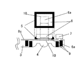
図42は、本発明の実施形態3として、本発明の実施形態1〜3の表示素子・撮像素子モジュールを表示部および撮像部に用いた電子情報機器の概略構成例を示すブロック図である。
(Embodiment 4)
FIG. 42 is a block diagram illustrating a schematic configuration example of an electronic information device using the display element / imaging device module according to Embodiments 1 to 3 of the present invention as a display unit and an imaging unit as Embodiment 3 of the present invention.

図42において、本実施形態4の電子情報機器90は、上記実施形態1〜3の表示素子・撮像素子モジュールの撮像素子モジュール20A〜20Dのいずれかからの撮像信号を各種信号処理してカラー画像信号を得る固体撮像装置91と、この固体撮像装置91からのカラー画像信号を記録用に所定の信号処理した後にデータ記録可能とする記録メディアなどのメモリ部92と、この固体撮像装置91からのカラー画像信号を表示用に所定の信号処理した後に表示素子2の液晶表示画面上に表示可能とする液晶表示装置などの表示手段93と、この固体撮像装置91からのカラー画像信号を通信用に所定の信号処理をした後に通信処理可能とする送受信装置などの通信手段94と、この固体撮像装置91からのカラー画像信号を印刷用に所定の信号処理をした後に印刷処理可能とするプリンタなどの画像出力手段95とを有している。なお、この電子情報機器90として、これに限らず、固体撮像装置91の他に、メモリ部92と、表示手段93と、通信手段94と、プリンタなどの画像出力手段95とのうちの少なくともいずれかを有していてもよい。当然のことながら、通信手段94で受信したカラー画像信号を表示用に所定の信号処理した後に液晶表示装置などの表示素子2の表示画面上に表示可能とする
この電子情報機器90としては、前述したように例えばデジタルビデオカメラ、デジタルスチルカメラなどのデジタルカメラや、監視カメラ、ドアホンカメラ、車載用前方監視カメラ(ドライブレコーダ)などの車載用カメラおよびテレビジョン電話用カメラなどの画像入力カメラ、スキャナ装置、ファクシミリ装置、カメラ付き携帯電話装置および携帯端末装置(PDA)などの画像入力デバイスを有した電子機器が考えられる。
In FIG. 42, the electronic information device 90 according to the fourth embodiment performs color signal processing on the imaging signals from any of the imaging element modules 20A to 20D of the display element / imaging element module according to the first to third embodiments. A solid-state imaging device 91 that obtains a signal, a memory unit 92 such as a recording medium that enables data recording after a predetermined signal processing is performed on the color image signal from the solid-state imaging device 91, and the solid-state imaging device 91 Display means 93 such as a liquid crystal display device that can display the color image signal on the liquid crystal display screen of the display element 2 after predetermined signal processing for display, and the color image signal from the solid-state imaging device 91 for communication. A communication means 94 such as a transmission / reception device capable of performing communication processing after predetermined signal processing and a color image signal from the solid-state imaging device 91 are predetermined for printing. And an image output means 95 such as a printer which allows printing process after the signal processing. The electronic information device 90 is not limited to this, but in addition to the solid-state imaging device 91, at least one of a memory unit 92, a display unit 93, a communication unit 94, and an image output unit 95 such as a printer. You may have. As a matter of course, the electronic information device 90 that can display the color image signal received by the communication means 94 on the display screen of the display element 2 such as a liquid crystal display device after predetermined signal processing for display is used. Thus, for example, digital cameras such as digital video cameras and digital still cameras, image input cameras and scanners such as surveillance cameras, door phone cameras, in-vehicle cameras such as in-vehicle front surveillance cameras (drive recorders), and television telephone cameras. An electronic device having an image input device such as a device, a facsimile machine, a mobile phone with camera, and a portable terminal (PDA) is conceivable.

したがって、本実施形態4によれば、この固体撮像装置91からのカラー画像信号に基づいて、これを表示画面上に良好に表示したり、これを紙面にて画像出力装置95により良好にプリントアウト(印刷)したり、これを通信データとして有線または無線にて良好に通信したり、これをメモリ部92に所定のデータ圧縮処理を行って良好に記憶したり、各種データ処理を良好に行うことができる。   Therefore, according to the fourth embodiment, on the basis of the color image signal from the solid-state imaging device 91, it is displayed on the display screen, or is printed out on the paper by the image output device 95. (Printing), communicating this as communication data in a wired or wireless manner, performing a predetermined data compression process in the memory unit 92 and storing it in a good manner, or performing various data processings satisfactorily Can do.

なお、上記実施形態4の電子情報機器90に限らず、本発明の表示素子・受光素子モジュールを情報記録再生部に用いた電子情報機器であってもよい。この場合の電子情報機器の光学素子としては、出射光を直進させて出射させると共に、入射光を曲げて所定方向に入射させる光学機能素子(例えばホログラム光学素子)である。また、電子情報機器の電子素子としては、出射光を発生させるための発光素子(例えば半導体レーザ素子またはレーザチップ)および入射光を受光するための受光素子(例えばフォトIC)を有している。   The electronic information device 90 according to the fourth embodiment is not limited to the electronic information device 90, and may be an electronic information device using the display element / light receiving element module of the present invention as an information recording / reproducing unit. The optical element of the electronic information device in this case is an optical function element (for example, a hologram optical element) that causes the emitted light to go straight and be emitted, and bends the incident light to be incident in a predetermined direction. Further, the electronic elements of the electronic information device have a light emitting element (for example, a semiconductor laser element or a laser chip) for generating emitted light and a light receiving element (for example, a photo IC) for receiving incident light.

以上のように、本発明の好ましい実施形態1〜4を用いて本発明を例示してきたが、本発明は、この実施形態1〜4に限定して解釈されるべきものではない。本発明は、特許請求の範囲によってのみその範囲が解釈されるべきであることが理解される。当業者は、本発明の具体的な好ましい実施形態1〜4の記載から、本発明の記載および技術常識に基づいて等価な範囲を実施することができることが理解される。本明細書において引用した特許、特許出願および文献は、その内容自体が具体的に本明細書に記載されているのと同様にその内容が本明細書に対する参考として援用されるべきであることが理解される。   As mentioned above, although this invention has been illustrated using preferable Embodiment 1-4 of this invention, this invention should not be limited and limited to this Embodiment 1-4. It is understood that the scope of the present invention should be construed only by the claims. It is understood that those skilled in the art can implement an equivalent range from the description of specific preferred embodiments 1 to 4 of the present invention based on the description of the present invention and the common general technical knowledge. Patents, patent applications, and documents cited herein should be incorporated by reference in their entirety, as if the contents themselves were specifically described herein. Understood.

本発明は、表示素子が配置された透明支持基板としてのガラス基板上に、被写体からの画像光を光電変換して撮像する半導体素子で構成された撮像素子を一体化させた受光素子一体型ディスプレイモジュールなどの表示素子・電子素子モジュールおよびその製造方法、この表示素子・電子素子モジュールを表示部および受光部に用いた例えばデジタルビデオカメラおよびデジタルスチルカメラなどのデジタルカメラや、画像入力カメラ、スキャナ、ファクシミリ、カメラ付き携帯電話装置、テレビジョン電話装置、テレビジョン装置や情報を表示する表示ユニットまたは表示装置などに搭載するディスプレイモジュールなどの電子情報機器の分野において、表示素子が配置されたガラス基板上に撮像素子、さらにレンズをも一体化させた構造とすることにより、更なるいっそうの部品点数の削減、実装面積の削減、配線効率の向上による端末の小型・薄型化および低消費電力化を実現することができる。   The present invention relates to a light receiving element integrated display in which an image pickup element composed of a semiconductor element that photoelectrically converts image light from a subject is imaged on a glass substrate as a transparent support substrate on which a display element is arranged. Display elements / electronic element modules such as modules and methods of manufacturing the same, digital cameras such as digital video cameras and digital still cameras, image input cameras, scanners, etc. In the field of electronic information equipment such as a facsimile, a camera-equipped mobile phone device, a television phone device, a television device, a display unit for displaying information or a display module mounted on a display device, etc. on a glass substrate on which a display element is arranged With an image sensor and lens By, it is possible to realize reduction of further parts further reduction of mounting area, a small, thin size and low power consumption of the terminal by improving the wiring efficiency.

本発明の実施形態1に係る表示素子・撮像素子モジュールの要部構成例を示す縦断面図である。It is a longitudinal cross-sectional view which shows the principal part structural example of the display element and image pick-up element module which concerns on Embodiment 1 of this invention. 図1の撮像素子部分を拡大した要部断面図である。It is principal part sectional drawing to which the image pick-up element part of FIG. 1 was expanded. 不要な赤外領域の波長をカットするためのIRカット材料をレンズ表面に形成する場合の構成例を示す撮像素子部分の要部断面図である。It is principal part sectional drawing of the image pick-up element part which shows the structural example in the case of forming IR cut material for cutting the wavelength of an unnecessary infrared region on the lens surface. 不要な赤外領域の波長をカットするためのIRカット材料を撮像素子表面に直接形成した場合の構成例を示す撮像素子部分の要部断面図である。It is principal part sectional drawing of the image pick-up element part which shows the structural example at the time of forming IR cut material for cutting the wavelength of an unnecessary infrared region directly on the image pick-up element surface. (a)は、図1のレンズ遮光層をガラス基板に形成するためのレジスト材料のパターニング例を示す要部断面図、(b)はその裏面図である。(A) is principal part sectional drawing which shows the example of patterning of the resist material for forming the lens light shielding layer of FIG. 1 in a glass substrate, (b) is the back view. 図5のレジスト材料をマスクとして、ガラス基板を異方性エッチングしてガラス基板に溝を形成する工程を示す要部断面図である。It is principal part sectional drawing which shows the process of forming a groove | channel in a glass substrate by anisotropically etching a glass substrate using the resist material of FIG. 5 as a mask. 図6のガラス基板の溝を遮光材料で埋め込む工程を示す要部断面図である。It is principal part sectional drawing which shows the process of embedding the groove | channel of the glass substrate of FIG. 6 with a light shielding material. 不要となったレジスト材料および余分な遮光材料を除去して形成された内側のレンズ遮光層を示す要部断面図である。It is principal part sectional drawing which shows the inner lens light-shielding layer formed by removing the resist material and unnecessary light-shielding material which became unnecessary. (a)は、図8のレンズ遮光層よりも一回り大きな外側のレンズ遮光層をレンズ遮光層形成面とは反対側の面から形成した場合の要部断面図、(b)は、(a)の変形例を示す要部断面図である。8A is a cross-sectional view of the main part when an outer lens light shielding layer that is slightly larger than the lens light shielding layer in FIG. 8 is formed from the surface opposite to the lens light shielding layer forming surface, and FIG. It is principal part sectional drawing which shows the modification of (). (a)は、図9の内側のレンズ遮光層と外側のレンズ遮光層とを入れ替えた場合の要部断面図、(b)は、(a)の変形例を示す要部断面図である。(A) is principal part sectional drawing at the time of replacing the inner lens light shielding layer and outer lens light shielding layer of FIG. 9, (b) is principal part sectional drawing which shows the modification of (a). 図1のレンズ形成面とは反対側の面に金属薄膜を形成した場合の要部断面図である。It is principal part sectional drawing at the time of forming a metal thin film in the surface on the opposite side to the lens formation surface of FIG. 図11の金属薄膜が多層金属膜で構成されていることを示す要部断面図である。It is principal part sectional drawing which shows that the metal thin film of FIG. 11 is comprised by the multilayer metal film. (a)は、図1のガラス基板に凸型のレンズを形成するためのレジスト材料のパタンーニング例を示す要部断面図、(b)は、(a)の裏面図である。(A) is principal part sectional drawing which shows the example of a patterning of the resist material for forming a convex lens in the glass substrate of FIG. 1, (b) is a back view of (a). 図1の凸型のレンズを形成するためのレジスト材料の熱硬化処理後の形状を示す要部断面図である。It is principal part sectional drawing which shows the shape after the thermosetting process of the resist material for forming the convex lens of FIG. 図1の凸型のレンズを異方性エッチングによりレジスト材料の形状をガラス基板に転写した場合を示す要部断面図である。FIG. 2 is a cross-sectional view of a main part showing a case where the shape of a resist material is transferred to a glass substrate by anisotropic etching of the convex lens of FIG. 1. (a)は、図1のガラス基板に凹型レンズを形成するためのレジスト材料のパターニング例を示す要部断面図、(b)は、(a)の裏面図である。(A) is principal part sectional drawing which shows the example of patterning of the resist material for forming a concave lens in the glass substrate of FIG. 1, (b) is a back view of (a). 図16のレジスト材料をマスクとしてガラス基板の等方性エッチングを行った場合の要部断面図である。It is principal part sectional drawing at the time of performing isotropic etching of a glass substrate using the resist material of FIG. 16 as a mask. 図17で不要となったレジスト材料を除去した場合の要部断面図である。It is principal part sectional drawing at the time of removing the resist material which became unnecessary in FIG. 図1の凸型のレンズを、別の方法として高温スタンパによるガラス基板への押圧により形成する場合の要部断面図である。It is principal part sectional drawing in the case of forming the convex lens of FIG. 1 by the press to the glass substrate by a high temperature stamper as another method. 図1の凸型のレンズを、更に別の方法として高温スタンパでフレネルレンズ形状を形成する場合の要部断面図である。FIG. 6 is a cross-sectional view of a main part when the convex lens of FIG. 1 is formed as a Fresnel lens shape with a high temperature stamper as still another method. 図16の凹型レンズを、更に別の方法として高温スタンパによるガラス基板への押圧により形成する場合の要部断面図である。FIG. 17 is a cross-sectional view of an essential part when the concave lens of FIG. 16 is formed by pressing the glass substrate with a high temperature stamper as still another method. IRカット材料をレンズ表面にコーティングするための工程を図示した要部断面図である。It is principal part sectional drawing which illustrated the process for coating IR cut material on the lens surface. (a)は、コーティングされたIRカット材料をパターニングするためのパターニング工程を図示した要部断面図であり、(b)は、その裏面図である。(A) is principal part sectional drawing which illustrated the patterning process for patterning the coated IR cut material, (b) is the back view. 図23のパターニング工程により、形成されたレンズ表面上のIRカット材料の形状を図示した要部断面図である。It is principal part sectional drawing which illustrated the shape of IR cut material on the lens surface formed by the patterning process of FIG. (a)は、レジスト膜をマスクとして撮像素子の配置面側のガラス基板の表面にIRカット材料を形成するIRカット材料形成工程を図示した平面図であり、(b)はその要部断面図である。(A) is the top view which illustrated the IR cut material formation process which forms IR cut material on the surface of the glass substrate of the arrangement surface side of an image pick-up element using a resist film as a mask, (b) is the principal part sectional drawing. It is. 図25のIRカット材料形成工程を経て形成されたIRカット材料の形状を図示した要部断面図である。It is principal part sectional drawing which illustrated the shape of IR cut material formed through the IR cut material formation process of FIG. 図1のガラス基板上に、表示装置、撮像素子およびその他素子群を接続するために金属薄膜の配線パターニングを行った状態を示す要部断面図である。It is principal part sectional drawing which shows the state which performed the wiring patterning of the metal thin film in order to connect a display apparatus, an image pick-up element, and another element group on the glass substrate of FIG. 遮光材料によって封止してガラス基板に配置された撮像素子およびその他素子群が金属薄膜で形成された配線パターンで接続された配置例を示した要部平面図および断面図である。It is the principal part top view and sectional drawing which showed the example of arrangement | positioning with which the image pick-up element sealed with the light shielding material and the other element group were connected with the wiring pattern formed with the metal thin film. 図1のガラス基板上のレンズに加えて、他のレンズ群を追加した場合の一構成例を示した要部断面図である。It is principal part sectional drawing which showed the example of 1 structure at the time of adding another lens group in addition to the lens on the glass substrate of FIG. 図1のガラス基板上のレンズに加えて、他のレンズ群を追加した場合の他の一構成例を示した要部断面図である。It is principal part sectional drawing which showed another structural example at the time of adding another lens group in addition to the lens on the glass substrate of FIG. 本発明の実施形態2に係る表示素子・撮像素子モジュールの要部構成例を示す縦断面図である。It is a longitudinal cross-sectional view which shows the principal part structural example of the display element and image pick-up element module which concerns on Embodiment 2 of this invention. 本発明の実施形態3に係る受光素子一体型液晶ディスプレイモジュールの構成例を示す要部断面図である。It is principal part sectional drawing which shows the structural example of the light receiving element integrated liquid crystal display module which concerns on Embodiment 3 of this invention. 本発明の実施形態3に係る受光素子一体型液晶ディスプレイモジュールの他の構成例を示す要部断面図である。It is principal part sectional drawing which shows the other structural example of the light receiving element integrated liquid crystal display module which concerns on Embodiment 3 of this invention. 本発明の実施形態3に係る受光素子一体型液晶ディスプレイモジュールの更に他の構成例を示す要部断面図である。It is principal part sectional drawing which shows the further another structural example of the light receiving element integrated liquid crystal display module which concerns on Embodiment 3 of this invention. 本発明の実施形態3に係る受光素子一体型液晶ディスプレイモジュールの更に他の構成例を示す要部断面図である。It is principal part sectional drawing which shows the further another structural example of the light receiving element integrated liquid crystal display module which concerns on Embodiment 3 of this invention. 本発明の実施形態3に係る受光素子一体型液晶ディスプレイモジュールの更に他の構成例を示す要部断面図である。It is principal part sectional drawing which shows the further another structural example of the light receiving element integrated liquid crystal display module which concerns on Embodiment 3 of this invention. 本発明の実施形態3に係る受光素子一体型液晶ディスプレイモジュールの更に他の構成例を示す要部断面図である。It is principal part sectional drawing which shows the further another structural example of the light receiving element integrated liquid crystal display module which concerns on Embodiment 3 of this invention. 本発明の実施形態3に係る受光素子一体型液晶ディスプレイモジュールの更に他の構成例を示す要部断面図である。It is principal part sectional drawing which shows the further another structural example of the light receiving element integrated liquid crystal display module which concerns on Embodiment 3 of this invention. 本発明の実施形態3に係る受光素子一体型液晶ディスプレイモジュールの更に他の構成例を示す要部断面図である。It is principal part sectional drawing which shows the further another structural example of the light receiving element integrated liquid crystal display module which concerns on Embodiment 3 of this invention. 本発明の実施形態3に係る受光素子一体型液晶ディスプレイモジュールの更に他の構成例を示す要部断面図である。It is principal part sectional drawing which shows the further another structural example of the light receiving element integrated liquid crystal display module which concerns on Embodiment 3 of this invention. 本発明の実施形態3に係る受光素子一体型液晶ディスプレイモジュールの更に他の構成例を示す要部断面図である。It is principal part sectional drawing which shows the further another structural example of the light receiving element integrated liquid crystal display module which concerns on Embodiment 3 of this invention. 本発明の実施形態4として、本発明の実施形態1〜3の表示素子・撮像素子モジュールを表示部および撮像部に用いた電子情報機器の概略構成例を示すブロック図である。It is a block diagram which shows the schematic structural example of the electronic information apparatus which used the display element and the image pick-up element module of Embodiment 1-3 of this invention for the display part and the imaging part as Embodiment 4 of this invention. 従来の液晶表示装置およびこれを接続する樹脂基板を示す斜視図である。It is a perspective view which shows the conventional liquid crystal display device and the resin substrate which connects this. 従来の液晶表示素子と複数の電子部品を同じ樹脂基板上に実装した場合の断面図である。It is sectional drawing at the time of mounting the conventional liquid crystal display element and several electronic components on the same resin substrate. 従来のCCD撮像素子と複数の電子部品を同じ樹脂基板上に実装した場合の断面図である。It is sectional drawing at the time of mounting the conventional CCD image pick-up element and several electronic components on the same resin substrate. 特許文献2に開示された従来の表示素子および撮像素子一体型構造を示す平面図である。FIG. 10 is a plan view showing a conventional display element and imaging element integrated structure disclosed in Patent Document 2.

符号の説明Explanation of symbols

1、1A 表示素子・撮像素子モジュール
2 表示装置
3 ガラス基板
4 レンズ
4a 凸レンズのレンズ形状
41 凹型レンズ
42 フレネルレンズのレンズ形状
5 遮光材料
6 撮像素子
6a 受光面
7 その他素子郡
8 3層の金属多層膜
8a 遮光用の金属薄膜
8b 絶縁膜
8c 配線用の金属薄膜
9 レンズ遮光層
9a 溝
9b 浅いレンズ遮光層
10 IRカット材料
11、12、13 レジスト膜
11a 遮光層形成用の円形線分パターン
12a、13a レンズ形成用の円形線分パターン
14 高温スタンパ
15,16 レジストパターン
15a IRカット材料を除去する部分
16a レジスト矩形パターン
17A、18A 2枚のレンズ群
18B 遮光部材(遮光ホルダ)
20、20A〜20C 撮像素子モジュール
51 受光素子一体型液晶ディスプレイモジュール(表示素子・撮像素子モジュール)
52 液晶ディスプレイ
53 透光性支持基板
54 電極パッド
55 受光素子チップ
56a ランド部
56b 配線部
57,57A 導電突起
58 導電粒子
59、59A〜59C 樹脂(接着樹脂)
60 受光領域
61 レンズユニット
64 絶縁膜
65 微小レンズ
66 カバー膜
71〜74 段差部
DESCRIPTION OF SYMBOLS 1, 1A Display element and image pick-up element module 2 Display apparatus 3 Glass substrate 4 Lens 4a Lens shape of convex lens 41 Concave lens 42 Lens shape of Fresnel lens 5 Light-shielding material 6 Image pick-up element 6a Light-receiving surface 7 Other element group 8 Three-layer metal multilayer Film 8a Metal thin film for light shielding 8b Insulating film 8c Metal thin film for wiring 9 Lens light shielding layer 9a Groove 9b Shallow lens light shielding layer 10 IR cut material 11, 12, 13 Resist film 11a Circular line segment pattern 12a for light shielding layer formation 13a Circular line segment pattern for lens formation 14 High temperature stamper 15, 16 Resist pattern 15a Part for removing IR cut material 16a Resist rectangular pattern 17A, 18A Two lens groups 18B Light shielding member (light shielding holder)
20, 20A-20C Image sensor module 51 Light receiving element integrated liquid crystal display module (display element / image sensor module)
52 Liquid crystal display 53 Translucent support substrate 54 Electrode pad 55 Light receiving element chip 56a Land part 56b Wiring part 57, 57A Conductive protrusion 58 Conductive particle 59, 59A-59C Resin (adhesive resin)
60 Light receiving area 61 Lens unit 64 Insulating film 65 Micro lens 66 Cover film 71-74 Stepped portion

Claims (41)

ディスプレイが配置された透光性支持基板において、該ディスプレイの配置箇所以外の透光性支持基板の一部にレンズを形成し、該レンズに対して電子素子が配置されている表示素子・電子素子モジュール。   A display element / electronic element in which a lens is formed on a part of the translucent support substrate other than the place where the display is arranged, and an electronic element is arranged with respect to the lens. module. 前記透光性支持基板に形成されたレンズの外周側に遮光層が設けられている請求項1に記載の表示素子・電子素子モジュール。   The display element / electronic element module according to claim 1, wherein a light shielding layer is provided on an outer peripheral side of a lens formed on the translucent support substrate. 前記遮光層で囲まれた透光性支持基板上で、前記レンズの光入射用中央部以外の透光性支持基板上に遮光膜が設けられている請求項2に記載の表示素子・電子素子モジュール。   3. The display element / electronic element according to claim 2, wherein a light-shielding film is provided on the translucent support substrate surrounded by the light-shielding layer, on the translucent support substrate other than the light incident central portion of the lens. module. 前記遮光層は、前記透光性支持基板上から形成された溝内に遮光材料が埋め込まれている請求項2または3に記載の表示素子・電子素子モジュール。   4. The display element / electronic element module according to claim 2, wherein the light shielding layer has a light shielding material embedded in a groove formed on the translucent support substrate. 5. 前記遮光層は、2重または3重に平面視円形状または楕円形状、四角形状に形成された前記透光性支持基板上から形成された溝内に遮光材料が埋め込まれている請求項2または3に記載の表示素子・電子素子モジュール。   The light-shielding material has a light-shielding material embedded in a groove formed on the translucent support substrate that is formed in a circular shape, an elliptical shape, or a quadrangular shape in a plan view in a double or triple manner. 4. The display element / electronic element module according to 3. 前記2重の遮光層の一方は、前記透光性支持基板の一方面側から形成された溝内に遮光材料が埋め込まれ、該2重の遮光層の他方は、該透光性支持基板の他方面側から形成された溝内に遮光材料が埋め込まれている請求項5に記載の表示素子・電子素子モジュール。   One of the double light shielding layers is embedded with a light shielding material in a groove formed from one side of the translucent support substrate, and the other of the double light shielding layers is formed on the translucent support substrate. The display element / electronic element module according to claim 5, wherein a light shielding material is embedded in a groove formed from the other surface side. 前記遮光用の金属膜上に絶縁膜を介して配線用の金属膜が設けられ、前記電子素子の各端子部は、該配線用の金属膜がパターニングされた配線層に接続されている請求項3に記載の表示素子・電子素子モジュール。   A metal film for wiring is provided on the light-shielding metal film via an insulating film, and each terminal portion of the electronic element is connected to a wiring layer in which the metal film for wiring is patterned. 4. The display element / electronic element module according to 3. 前記電子素子と前記透光性支持基板の間が遮光材料で封止されている請求項1に記載の表示素子・電子素子モジュール。   The display element / electronic element module according to claim 1, wherein a space between the electronic element and the translucent support substrate is sealed with a light shielding material. 前記電子素子としての撮像素子からの画像データに基づいて前記ディスプレイに直接表示するべく、該ディスプレイが前記透光性支持基板上の金属膜の配線パターンにより該撮像素子と接続される配線経路が設けられている請求項1に記載の表示素子・電子素子モジュール。   In order to display directly on the display based on image data from the image sensor as the electronic element, a wiring path is provided in which the display is connected to the image sensor by a wiring pattern of a metal film on the translucent support substrate. The display element / electronic element module according to claim 1. 前記レンズと前記電子素子としての受光素子の受光領域との間にIRカット材料が設けられている請求項1に記載の表示素子・電子素子モジュール。   The display element / electronic element module according to claim 1, wherein an IR cut material is provided between the lens and a light receiving region of a light receiving element as the electronic element. 前記IRカット材料は、前記レンズ曲面上、該レンズ曲面が形成される側とは反対の透光性支持基板面上および前記受光素子の受光領域の表面上のいずれかに設けられている請求項10に記載の表示素子・電子素子モジュール。   The IR cut material is provided either on the curved surface of the lens, on the surface of the light-transmitting support substrate opposite to the side on which the curved surface of the lens is formed, or on the surface of the light receiving region of the light receiving element. 10. The display element / electronic element module according to 10. 前記透光性支持基板のレンズは、凹型レンズおよび凸型レンズのいずれかである請求項1に記載の表示素子・電子素子モジュール。   The display element / electronic element module according to claim 1, wherein the lens of the translucent support substrate is one of a concave lens and a convex lens. 前記電子素子には、素子領域を囲む周辺領域に一または複数の電極部が配設されており、ディスプレイを構成する透光性支持基板の配線部に該電極部上の導電突起を用いて該電子素子を接続する接続構造において、該透光性支持基板と該電子素子との間の該素子領域に対応する領域を避けるように、該透光性支持基板と該電子素子との間の少なくとも該接続構造が樹脂で固められた実装構造を有する請求項1に記載の表示素子・電子素子モジュール。   In the electronic device, one or a plurality of electrode portions are disposed in a peripheral region surrounding the device region, and a conductive protrusion on the electrode portion is used for the wiring portion of the translucent support substrate constituting the display. In a connection structure for connecting an electronic element, at least between the translucent support substrate and the electronic element so as to avoid a region corresponding to the element region between the translucent support substrate and the electronic element. The display element / electronic element module according to claim 1, wherein the connection structure has a mounting structure solidified with a resin. 前記透光性支持基板の配線部と前記電極部上の導電突起との間に異方性導電樹脂材料の導電粒子を介在させた接続部分を完全に覆うように前記樹脂で固められている請求項13に記載の表示素子・電子素子モジュール。   Claims: The resin is solidified so as to completely cover a connection portion in which conductive particles of an anisotropic conductive resin material are interposed between a wiring portion of the translucent support substrate and a conductive protrusion on the electrode portion. Item 14. The display element / electronic element module according to Item 13. 前記透光性支持基板と前記電子素子との間の接続構造を含む周辺領域が前記樹脂で固められている請求項13に記載の表示素子・電子素子モジュール。   The display element / electronic element module according to claim 13, wherein a peripheral region including a connection structure between the translucent support substrate and the electronic element is fixed with the resin. 前記素子領域に対応する領域に前記樹脂が広がるのを食い止めるための突状の段差部が、前記電子素子の周辺領域、および該周辺領域に対向する前記透光性支持基板の領域のうちの少なくともいずれかに設けられている請求項13〜15のいずれかに記載の表示素子・電子素子モジュール。   A projecting stepped portion for preventing the resin from spreading in a region corresponding to the device region includes at least one of a peripheral region of the electronic device and a region of the translucent support substrate facing the peripheral region. The display element / electronic element module according to claim 13, which is provided in any one of the above. 前記樹脂が外側に広がるのを食い止めるための突状の段差部が、前記電子素子の周辺部、および前記透光性支持基板における該電子素子と対向する領域の周辺部のうちの少なくともいずれかに設けられている請求項13〜16のいずれかに記載の表示素子・電子素子モジュール。   The protruding stepped portion for preventing the resin from spreading outward is at least one of a peripheral portion of the electronic element and a peripheral portion of the region facing the electronic element in the translucent support substrate. The display element / electronic element module according to claim 13, which is provided. 前記素子領域に対応する領域に前記樹脂が広がるのを食い止めるべく、該樹脂をはじく性質を有する材料が、前記電子素子の周辺領域、および該周辺領域に対向する前記透光性支持基板の領域のうちの少なくともいずれかに設けられている請求項13〜15のいずれかに記載の表示素子・電子素子モジュール。   In order to prevent the resin from spreading in a region corresponding to the device region, a material having a property of repelling the resin is formed in a peripheral region of the electronic device and a region of the translucent support substrate facing the peripheral region. The display element / electronic element module according to claim 13, wherein the display element / electronic element module is provided in at least one of them. 前記樹脂が外側に広がるのを食い止めるべく、該樹脂をはじく性質を有する材料が、前記電子素子の周辺部、および前記透光性支持基板における該電子素子と対向する領域の周辺部のうちの少なくともいずれかに設けられている請求項13〜15および18のいずれかに記載の表示素子・電子素子モジュール。   In order to prevent the resin from spreading outward, a material having a property of repelling the resin is at least one of a peripheral part of the electronic element and a peripheral part of the region facing the electronic element in the translucent support substrate. The display element / electronic element module according to claim 13, which is provided in any one of the above. 前記電子素子の周辺部は、該電子素子の端部およびその外側近傍である請求項17または19に記載の表示素子・電子素子モジュール。   20. The display element / electronic element module according to claim 17 or 19, wherein a peripheral part of the electronic element is an end part of the electronic element and the vicinity thereof. 前記外側近傍の更に周辺部に封止樹脂が設けられ、該封止樹脂により前記透光性支持基板と該電子素子との間を封止している請求項20に記載の表示素子・電子素子モジュール。   21. The display element / electronic element according to claim 20, wherein a sealing resin is further provided in a peripheral portion near the outside, and the space between the translucent support substrate and the electronic element is sealed by the sealing resin. module. 前記封止樹脂は、該電子素子の側面と上面を覆っている請求項21に記載の表示素子・電子素子モジュール。   The display element / electronic element module according to claim 21, wherein the sealing resin covers a side surface and an upper surface of the electronic element. 前記突状の段差部の少なくとも表面部が、前記樹脂をはじく性質を有する材料で構成されている請求項16または17に記載の表示素子・電子素子モジュール。   The display element / electronic element module according to claim 16 or 17, wherein at least a surface portion of the protruding stepped portion is made of a material having a property of repelling the resin. 前記樹脂は、少なくとも前記接続構造の接続部分に導電粒子を含有する樹脂が設けられている請求項13または15に記載の表示素子・電子素子モジュール。   The display element / electronic element module according to claim 13, wherein the resin is provided with a resin containing conductive particles at least in a connection portion of the connection structure. 前記導電粒子を含有する樹脂材料は異方性導電樹脂材料である請求項13または15に記載の表示素子・電子素子モジュール。   The display element / electronic element module according to claim 13 or 15, wherein the resin material containing the conductive particles is an anisotropic conductive resin material. 前記樹脂は、非導電粒子を含有する樹脂を少なくとも一部に有する請求項13〜15、24および25のいずれかに記載の表示素子・電子素子モジュール。   The display element / electronic element module according to claim 13, wherein the resin has a resin containing non-conductive particles in at least a part thereof. 前記樹脂は、遮光性樹脂を少なくとも一部に有する請求項13〜15、20〜22、24および26のいずれかに記載の表示素子・電子素子モジュール。   The display element / electronic element module according to any one of claims 13 to 15, 20 to 22, 24, and 26, wherein the resin has a light-shielding resin in at least a part thereof. 前記段差部は、前記ディスプレイを構成する材料と共通材料から構成されている請求項16、17および23のいずれかに記載の表示素子・電子素子モジュール。   The display element / electronic element module according to any one of claims 16, 17 and 23, wherein the step portion is made of a material and a common material constituting the display. 前記樹脂をはじく材料は、前記ディスプレイを構成する材料と共通材料から構成されている請求項18、19および23のいずれかに記載の表示素子・電子素子モジュール。   The display element / electronic element module according to any one of claims 18, 19 and 23, wherein the material that repels the resin is composed of a material common to the material constituting the display. 前記段差部は、前記電子素子上の膜を構成する材料と共通材料から構成されている請求項16、17および23のいずれかに記載の表示素子・電子素子モジュール。   The display element / electronic element module according to any one of claims 16, 17 and 23, wherein the stepped portion is made of a material and a common material constituting a film on the electronic element. 前記段差部は、電磁波により硬化する材料から構成されている請求項16、17および23のいずれかに記載の表示素子・電子素子モジュール。   24. The display element / electronic element module according to claim 16, wherein the step portion is made of a material that is cured by electromagnetic waves. 前記透光性支持基板は、貫通配線または/および側面配線により接続された両面配線を有している請求項13〜15のいずれかに記載の表示素子・電子素子モジュール。   The display element / electronic element module according to claim 13, wherein the translucent support substrate has a double-sided wiring connected by through wiring or / and side wiring. 前記ディスプレイが配設されている透光性支持基板の面とは反対側の面に前記電子素子が配設され、前記両面配線を用いて該ディスプレイと該電子素子とが電気的に接続されている請求項32に記載の表示素子・電子素子モジュール。   The electronic element is disposed on a surface opposite to the surface of the translucent support substrate on which the display is disposed, and the display and the electronic element are electrically connected using the double-sided wiring. The display element / electronic element module according to claim 32. 前記電子素子は受光素子である請求項1または13に記載の表示素子・電子素子モジュール。   The display element / electronic element module according to claim 1, wherein the electronic element is a light receiving element. 前記電子素子は、入射光を光電変換して撮像する複数の受光部が設けられた撮像素子である請求項1または13に記載の表示素子・電子素子モジュール。   14. The display element / electronic element module according to claim 1, wherein the electronic element is an imaging element provided with a plurality of light receiving units that photoelectrically convert incident light to image. 前記透光性支持基板は、ガラス基板または樹脂基板のいずれかである請求項1または13に記載の表示素子・電子素子モジュール。   The display element / electronic element module according to claim 1, wherein the translucent support substrate is a glass substrate or a resin substrate. 請求項1に記載の表示素子・電子素子モジュールの製造方法であって、前記ディスプレイが配置された透光性支持基板において、該ディスプレイの配置箇所以外の透光性支持基板の一部にレンズを形成するレンズ形成工程と、該レンズに対して電子素子を配置する電子素子配置工程とを有する表示素子・電子素子モジュールの製造方法。   The method of manufacturing a display element / electronic element module according to claim 1, wherein a lens is provided on a part of the light-transmitting support substrate other than the display location in the light-transmitting support substrate on which the display is disposed. A manufacturing method of a display element / electronic element module, comprising: a lens forming step to be formed; and an electronic element arranging step of arranging an electronic element with respect to the lens. 前記レンズ形成工程は、パターニングされたレジスト膜を熱処理した後のレジスト膜表面形状を、エッチングにより前記透光性支持基板に転写するかまたは、高温スタンパによる該透光性支持基板への押圧によってレンズ表面を形成する請求項37に記載の表示素子・電子素子モジュールの製造方法。   In the lens forming step, the resist film surface shape after heat-treating the patterned resist film is transferred to the translucent support substrate by etching, or the lens is formed by pressing the translucent support substrate with a high temperature stamper. The method for manufacturing a display element / electronic element module according to claim 37, wherein the surface is formed. 前記レンズ形成工程は、前記透光性支持基板から形成されたレンズに対応するように一または複数のレンズがホルダに保持された状態で固定されている請求項37または38に記載の表示素子・電子素子モジュールの製造方法。   39. The display element according to claim 37 or 38, wherein in the lens forming step, one or a plurality of lenses are fixed in a state of being held by a holder so as to correspond to a lens formed from the translucent support substrate. Manufacturing method of electronic element module. 請求項1〜36のいずれかに記載の表示素子・電子素子モジュールを表示部および撮像部に用いた電子情報機器。   An electronic information device using the display element / electronic element module according to any one of claims 1 to 36 for a display unit and an imaging unit. 請求項1〜33および36のいずれかに記載の表示素子・電子素子モジュールを表示部、発光部および受光部に用いた電子情報機器。   The electronic information device which used the display element and electronic element module in any one of Claims 1-33 and 36 for the display part, the light emission part, and the light-receiving part.
JP2008206440A 2008-08-08 2008-08-08 Display element / electronic element module and electronic information device Expired - Fee Related JP5037450B2 (en)

Priority Applications (2)

Application Number Priority Date Filing Date Title
JP2008206440A JP5037450B2 (en) 2008-08-08 2008-08-08 Display element / electronic element module and electronic information device
US12/462,525 US8704961B2 (en) 2008-08-08 2009-08-05 Display element having a lens being formed as part of a translucent support substrate having a display disposed thereon

Applications Claiming Priority (1)

Application Number Priority Date Filing Date Title
JP2008206440A JP5037450B2 (en) 2008-08-08 2008-08-08 Display element / electronic element module and electronic information device

Publications (2)

Publication Number Publication Date
JP2010045463A true JP2010045463A (en) 2010-02-25
JP5037450B2 JP5037450B2 (en) 2012-09-26

Family

ID=41652584

Family Applications (1)

Application Number Title Priority Date Filing Date
JP2008206440A Expired - Fee Related JP5037450B2 (en) 2008-08-08 2008-08-08 Display element / electronic element module and electronic information device

Country Status (2)

Country Link
US (1) US8704961B2 (en)
JP (1) JP5037450B2 (en)

Cited By (6)

* Cited by examiner, † Cited by third party
Publication number Priority date Publication date Assignee Title
JP2012098726A (en) * 2010-10-29 2012-05-24 Apple Inc Camera lens structures and display structures for electronic devices
JP2014057271A (en) * 2012-09-13 2014-03-27 Sharp Corp Camera module and display device
JP2017142497A (en) * 2012-01-10 2017-08-17 アップル インコーポレイテッド Integrated type camera window
WO2017203592A1 (en) * 2016-05-24 2017-11-30 オリンパス株式会社 Endoscope optical unit, endoscope, and method for manufacturing endoscope optical unit
JP2019197886A (en) * 2018-05-07 2019-11-14 キヤノン株式会社 Printed circuit board, manufacturing method of printed circuit board and electronic apparatus
WO2020080154A1 (en) * 2018-10-15 2020-04-23 ソニーセミコンダクタソリューションズ株式会社 Sensor module and electronic apparatus

Families Citing this family (22)

* Cited by examiner, † Cited by third party
Publication number Priority date Publication date Assignee Title
US8743309B2 (en) 2009-11-10 2014-06-03 Apple Inc. Methods for fabricating display structures
TWI452550B (en) * 2010-07-23 2014-09-11 Pixart Imaging Inc Display panel and an assembly method thereof
US8779452B2 (en) * 2010-09-02 2014-07-15 Tzu-Hsiang HUNG Chip package
US8467177B2 (en) 2010-10-29 2013-06-18 Apple Inc. Displays with polarizer windows and opaque masking layers for electronic devices
KR101285393B1 (en) * 2011-12-01 2013-07-10 주식회사 팬택 Mobile communication terminal including camera module
CN103021278B (en) * 2012-12-07 2015-08-19 京东方科技集团股份有限公司 A kind of display panel and display device
GB2509764B (en) * 2013-01-14 2018-09-12 Kaleido Tech Aps A lens array and a method of making a lens array
US9488891B2 (en) * 2013-04-22 2016-11-08 National University Of Singapore Thin-surface liquid crystal based voltage sensor
CN105793979B (en) * 2013-12-27 2019-05-28 英特尔公司 Optoelectronic packaging component
KR101534992B1 (en) * 2013-12-31 2015-07-07 현대자동차주식회사 Method for forming nanopattern of lens surface and lens having nanopattern of lens surface
CN105812632A (en) * 2016-03-25 2016-07-27 信利光电股份有限公司 Circuit board and camera module thereof
JP6904338B2 (en) * 2016-04-27 2021-07-14 Agc株式会社 Window members and vehicle window glass
EP3471391B1 (en) * 2017-10-10 2020-08-12 Axis AB A camera
CN108196388B (en) * 2018-02-12 2022-04-19 京东方科技集团股份有限公司 Display device and manufacturing method thereof
US11282717B2 (en) * 2018-03-30 2022-03-22 Intel Corporation Micro-electronic package with substrate protrusion to facilitate dispense of underfill between a narrow die-to-die gap
CN110418032A (en) * 2018-04-28 2019-11-05 南昌欧菲光电技术有限公司 Camera module and electronic device
US11382209B2 (en) * 2018-05-07 2022-07-05 Canon Kabushiki Kaisha Method for manufacturing printed circuit board, printed circuit board, and electronic device
JP2020013928A (en) * 2018-07-19 2020-01-23 ソニーセミコンダクタソリューションズ株式会社 Imaging element and electronic apparatus
CN112313568B (en) * 2019-04-30 2022-06-17 京东方科技集团股份有限公司 Display device
US11637919B2 (en) 2019-12-03 2023-04-25 Apple Inc. Handheld electronic device
US11522983B2 (en) 2019-12-03 2022-12-06 Apple Inc. Handheld electronic device
CN112969010A (en) * 2021-02-02 2021-06-15 维沃移动通信有限公司 Electronic device

Citations (1)

* Cited by examiner, † Cited by third party
Publication number Priority date Publication date Assignee Title
JPH11317894A (en) * 1998-03-05 1999-11-16 Olympus Optical Co Ltd Optical device

Family Cites Families (3)

* Cited by examiner, † Cited by third party
Publication number Priority date Publication date Assignee Title
JPH0514880A (en) 1991-06-28 1993-01-22 Toshiba Corp Visual telephone
JPH09244007A (en) 1996-03-11 1997-09-19 Matsushita Electric Ind Co Ltd Liquid crystal display device, ccd image pickup device and their production
KR20080035601A (en) * 2005-08-08 2008-04-23 코니카 미놀타 옵토 인코포레이티드 Imaging device and assembling method for imaging device

Patent Citations (1)

* Cited by examiner, † Cited by third party
Publication number Priority date Publication date Assignee Title
JPH11317894A (en) * 1998-03-05 1999-11-16 Olympus Optical Co Ltd Optical device

Cited By (10)

* Cited by examiner, † Cited by third party
Publication number Priority date Publication date Assignee Title
JP2012098726A (en) * 2010-10-29 2012-05-24 Apple Inc Camera lens structures and display structures for electronic devices
US9143668B2 (en) 2010-10-29 2015-09-22 Apple Inc. Camera lens structures and display structures for electronic devices
US10009525B2 (en) 2010-10-29 2018-06-26 Apple Inc. Camera lens structures and display structures for electronic devices
JP2017142497A (en) * 2012-01-10 2017-08-17 アップル インコーポレイテッド Integrated type camera window
JP2014057271A (en) * 2012-09-13 2014-03-27 Sharp Corp Camera module and display device
WO2017203592A1 (en) * 2016-05-24 2017-11-30 オリンパス株式会社 Endoscope optical unit, endoscope, and method for manufacturing endoscope optical unit
US10742856B2 (en) 2016-05-24 2020-08-11 Olympus Corporation Optical unit for endoscope, endoscope and method for manufacturing optical unit for endoscope
JP2019197886A (en) * 2018-05-07 2019-11-14 キヤノン株式会社 Printed circuit board, manufacturing method of printed circuit board and electronic apparatus
JP7362286B2 (en) 2018-05-07 2023-10-17 キヤノン株式会社 Printed circuit board manufacturing method, printed circuit board, and electronic equipment
WO2020080154A1 (en) * 2018-10-15 2020-04-23 ソニーセミコンダクタソリューションズ株式会社 Sensor module and electronic apparatus

Also Published As

Publication number Publication date
JP5037450B2 (en) 2012-09-26
US20100033647A1 (en) 2010-02-11
US8704961B2 (en) 2014-04-22

Similar Documents

Publication Publication Date Title
JP5037450B2 (en) Display element / electronic element module and electronic information device
JP2010045082A (en) Display element/electronic element module and its manufacturing method, and electronic information equipment
US11043436B2 (en) Semiconductor device, manufacturing method, imaging device, and electronic apparatus for enabling component mounting with high flatness
US6784409B2 (en) Electronic device with encapsulant of photo-set resin and production process of same
JP5375219B2 (en) Imaging device
JP2005352314A (en) Imaging device and electronic apparatus
JP2007073958A (en) Wafer level chip size package for image sensor module and method of manufacturing same
JP2008305972A (en) Optical device, its manufacturing method, camera module using optical device and electronic apparatus loading camera module
JP2007012995A (en) Microminiature camera module and method of manufacturing same
JP6787378B2 (en) Interposer board
JP5392458B2 (en) Semiconductor image sensor
US20060138579A1 (en) Image sensor package, solid state imaging device, and fabrication methods thereof
KR20200063102A (en) Filming assembly and its packaging method, lens module, electronic device
JP2008277593A (en) Circuit board, optical device employing the same, camera module, and manufacturing method for the circuit board
JP2010219948A (en) Display panel and method of manufacturing same
US7888157B2 (en) Image sensor chip package method
US20220084923A1 (en) Chip package structure and method for manufacturing the same, and module
JPWO2018047635A1 (en) Solid-state imaging device, manufacturing method, and electronic device
JP2006261380A (en) Optical communication module
KR20080005733A (en) Image sensor module and camera module
JP4923967B2 (en) Solid-state imaging device and electronic apparatus
KR20090073656A (en) Camera module and manufacturing method thereof
JP4292383B2 (en) Optical device manufacturing method
JP5599294B2 (en) Imaging module, manufacturing method thereof, and electronic information device
JP2009070876A (en) Solid-state imaging device and its manufacturing process

Legal Events

Date Code Title Description
A621 Written request for application examination

Free format text: JAPANESE INTERMEDIATE CODE: A621

Effective date: 20100826

A977 Report on retrieval

Free format text: JAPANESE INTERMEDIATE CODE: A971007

Effective date: 20111213

A131 Notification of reasons for refusal

Free format text: JAPANESE INTERMEDIATE CODE: A131

Effective date: 20120105

A521 Request for written amendment filed

Free format text: JAPANESE INTERMEDIATE CODE: A523

Effective date: 20120126

TRDD Decision of grant or rejection written
A01 Written decision to grant a patent or to grant a registration (utility model)

Free format text: JAPANESE INTERMEDIATE CODE: A01

Effective date: 20120613

A01 Written decision to grant a patent or to grant a registration (utility model)

Free format text: JAPANESE INTERMEDIATE CODE: A01

A61 First payment of annual fees (during grant procedure)

Free format text: JAPANESE INTERMEDIATE CODE: A61

Effective date: 20120704

FPAY Renewal fee payment (event date is renewal date of database)

Free format text: PAYMENT UNTIL: 20150713

Year of fee payment: 3

R150 Certificate of patent or registration of utility model

Free format text: JAPANESE INTERMEDIATE CODE: R150

RD04 Notification of resignation of power of attorney

Free format text: JAPANESE INTERMEDIATE CODE: R3D04

LAPS Cancellation because of no payment of annual fees