JP2010041020A - Transient noise detection circuit - Google Patents
Transient noise detection circuit Download PDFInfo
- Publication number
- JP2010041020A JP2010041020A JP2008262741A JP2008262741A JP2010041020A JP 2010041020 A JP2010041020 A JP 2010041020A JP 2008262741 A JP2008262741 A JP 2008262741A JP 2008262741 A JP2008262741 A JP 2008262741A JP 2010041020 A JP2010041020 A JP 2010041020A
- Authority
- JP
- Japan
- Prior art keywords
- unit
- circuit
- transient noise
- rectifier
- detection circuit
- Prior art date
- Legal status (The legal status is an assumption and is not a legal conclusion. Google has not performed a legal analysis and makes no representation as to the accuracy of the status listed.)
- Granted
Links
Images


Classifications
-
- G—PHYSICS
- G01—MEASURING; TESTING
- G01R—MEASURING ELECTRIC VARIABLES; MEASURING MAGNETIC VARIABLES
- G01R19/00—Arrangements for measuring currents or voltages or for indicating presence or sign thereof
- G01R19/0046—Arrangements for measuring currents or voltages or for indicating presence or sign thereof characterised by a specific application or detail not covered by any other subgroup of G01R19/00
- G01R19/0053—Noise discrimination; Analog sampling; Measuring transients
-
- G—PHYSICS
- G01—MEASURING; TESTING
- G01R—MEASURING ELECTRIC VARIABLES; MEASURING MAGNETIC VARIABLES
- G01R19/00—Arrangements for measuring currents or voltages or for indicating presence or sign thereof
- G01R19/04—Measuring peak values or amplitude or envelope of ac or of pulses
-
- G—PHYSICS
- G01—MEASURING; TESTING
- G01R—MEASURING ELECTRIC VARIABLES; MEASURING MAGNETIC VARIABLES
- G01R29/00—Arrangements for measuring or indicating electric quantities not covered by groups G01R19/00 - G01R27/00
- G01R29/26—Measuring noise figure; Measuring signal-to-noise ratio
-
- G—PHYSICS
- G01—MEASURING; TESTING
- G01R—MEASURING ELECTRIC VARIABLES; MEASURING MAGNETIC VARIABLES
- G01R31/00—Arrangements for testing electric properties; Arrangements for locating electric faults; Arrangements for electrical testing characterised by what is being tested not provided for elsewhere
- G01R31/001—Measuring interference from external sources to, or emission from, the device under test, e.g. EMC, EMI, EMP or ESD testing
- G01R31/002—Measuring interference from external sources to, or emission from, the device under test, e.g. EMC, EMI, EMP or ESD testing where the device under test is an electronic circuit
Abstract
Description
本発明はトランジェントノイズ検出に関する。特に、本発明はトランジェントノイズ検出回路に関する。 The present invention relates to transient noise detection. In particular, the present invention relates to a transient noise detection circuit.
ICにおけるデバイス規模が小さくなると、デバイスは例えば静電放電(ESD)又は電気的な速いトランジェント(EFT)のような速いノイズトランジェント事象に、より脆弱になってきた。従って、ESDはIC製品にとって最重要な信頼性問題の1つとなり、全てのICの設計段階で考慮しなければならない。 As device scale in ICs has decreased, devices have become more vulnerable to fast noise transient events such as electrostatic discharge (ESD) or electrical fast transients (EFT). Therefore, ESD is one of the most important reliability issues for IC products and must be considered at the design stage of all ICs.
ユニットレベルのESD問題の他に、システムレベルのESD問題もCMOS IC製品における高まる重要な信頼性問題である。あるCMOS ICは、それらが±2KVの人体モデル(HBM)、±200Vの機械モデル(MM)、及び±1KVの荷電装置モデル(CDM)のようなユニットレベルESD仕様をパスしたとしても、システムレベルESD圧力には非常に影響を受け易い。 In addition to unit level ESD issues, system level ESD issues are also an increasingly important reliability issue in CMOS IC products. Some CMOS ICs are system level even if they pass unit level ESD specifications such as ± 2KV human body model (HBM), ± 200V mechanical model (MM), and ± 1KV charged device model (CDM). Very sensitive to ESD pressure.
システムレベルESD試験で、通常電力がICの内部回路に提供され、そして内部回路はそれらの初期機能を実施するように作動する。システムレベルESD試験の目的は内部回路がESDノイズにさえ干渉される通常動作を保持することができるかどうか、又は回路がそれらを回復するように自動的にリセットできるかどうかを決定することである。システムレベルのESD試験標準IEC61000‐4‐2で、電子製品は、“レベル4”の耐性要求を満足するため、接触放電試験で+8KV、及び空中放電試験で+15kVのESDレベルを維持しなければならない。高エネルギーESD誘導ノイズは、しばしば試験(EUT)下の装置内でCMOSICの故障又は誤動作を起こす。 In system level ESD testing, normal power is provided to the internal circuitry of the IC, and the internal circuitry operates to perform their initial functions. The purpose of system level ESD testing is to determine whether internal circuits can maintain normal operation that is even disturbed by ESD noise, or whether the circuit can automatically reset to recover them. . Under the system level ESD test standard IEC61000-4-2, electronic products must maintain ESD levels of + 8KV in contact discharge tests and + 15kV in air discharge tests to meet "level 4" durability requirements. . High energy ESD induced noise often causes CMOS IC failures or malfunctions in devices under test (EUT).
図1は、ICチップ内のシステムレベルESD検出回路16と内部回路14の接続関係を示す。通常の電源オン状態下で、電源オン/リセット回路12は内部回路14を起動させ、そしてESD検出回路16をリセットする。その後、内部回路14はその初期動作を開始し、そしてESD検出回路16はESD事象の検出を開始する。一旦突然の電圧オーバシュート又はアンダシュートが電源レール(VDD又はVSS)に発生すると、ESD検出回路16は内部回路14に対し保護処理を実施するため電源オン/リセット回路12へ知らせる。
FIG. 1 shows a connection relationship between the system level ESD detection circuit 16 and the
実際の適用では、異なる保護処理が様々なファームウェア又は回路設計を有する、異なるICで使用される。例えば、電源オン/リセット回路12は内部回路14の全体又は一部のみをリセットする。そうすることにより、チップ全体のより重大な誤動作を防止することができる。
In practical applications, different protection processes are used in different ICs with different firmware or circuit designs. For example, the power-on /
システムレベルESD検出回路は、IEEE Trans電磁互換性、50巻、No1、1〜9ページ、2008年2月のM.-D.Ker、C.-C.Yen、とP.-C.Shihにより報告された“電磁互換性規定を満足させるためのCMOS集積回路のシステムレベルESD保護のためのオンチップトランジェント検出回路”で提案されている。図2を参照されたい。図2に上述の論文のESD検出回路を示す。 System level ESD detection circuit is based on IEEE Trans electromagnetic compatibility, 50, No. 1, 1-9, February 2008 by M.-D.Ker, C.-C.Yen, and P.-C. Shih It has been proposed in the reported "On-chip transient detection circuit for system level ESD protection of CMOS integrated circuits to meet electromagnetic compatibility regulations". Please refer to FIG. FIG. 2 shows the ESD detection circuit of the above paper.
図2に示すように、キャパシタCp1とCp2は夫々システムがESD事象を受ける場合に、VDDとVSS上に発生する速いトランジェントを検出するために使用される。その結果、図2の回路はシステムレベルのESDノイズを検出することができ、ESDトランジェント事象を伝達するため、出力信号を電源オン/リセット内部回路へ伝送する。内部回路がESDとトランジェントノイズを処理した後、検出回路を再度リセットすることができる。 As shown in FIG. 2, capacitors C p1 and C p2 are used to detect fast transients that occur on V DD and V SS when the system receives an ESD event, respectively. As a result, the circuit of FIG. 2 can detect system level ESD noise and transmits the output signal to the power on / reset internal circuit to convey the ESD transient event. After the internal circuit processes ESD and transient noise, the detection circuit can be reset again.
従来技術で、検出回路はシステムレベルESDトランジェントノイズを結合するため、受動装置(キャパシタCp1とCp2)を使用する。しかし受動装置によりESDトランジェントノイズを結合するためのこの技術は、例えば内臓コネクタの寄生キャパシタのようなシステム上の寄生負荷により激しく影響される。 In the prior art, the detection circuit uses passive devices (capacitors C p1 and C p2 ) to couple system level ESD transient noise. However, this technique for coupling ESD transient noise with passive devices is severely affected by parasitic loads on the system, such as the parasitic capacitors of built-in connectors.
上記問題を解決するため、本発明の範囲は、トランジェントノイズ電圧レベルを判定できるトランジェントノイズ検出回路を提供することである。 In order to solve the above problem, the scope of the present invention is to provide a transient noise detection circuit capable of determining a transient noise voltage level.
本発明による一実施例はESD検出回路である。ESD検出回路はESD電圧レベルを検出するために使用される。ESD検出回路はトリガ回路、整流回路、及び制御装置を備える。 One embodiment according to the present invention is an ESD detection circuit. The ESD detection circuit is used to detect the ESD voltage level. The ESD detection circuit includes a trigger circuit, a rectifier circuit, and a control device.
トリガ回路は電源レールとアースノード間に接続される。トリガ回路がトランジェントノイズを受信すると、トリガ回路はトリガ信号を発生させる。整流回路はトリガ回路、電源レール、及びアースノードへ接続される。整流回路は直列接続される整流回路、及び電流制御ユニットを備える。 The trigger circuit is connected between the power rail and the ground node. When the trigger circuit receives the transient noise, the trigger circuit generates a trigger signal. The rectifier circuit is connected to the trigger circuit, the power rail, and the ground node. The rectifier circuit includes a rectifier circuit connected in series and a current control unit.
実際の適用では、整流ユニットはシリコン制御整流器(SCR)装置を備え、電流制限ユニットは少なくとも1つのMOSFET(金属酸化物半導体電界効果トランジスタ)装置を備える。 In practical applications, the rectifying unit comprises a silicon controlled rectifier (SCR) device and the current limiting unit comprises at least one MOSFET (metal oxide semiconductor field effect transistor) device.
整流ユニットがトリガ回路からトリガ信号を受信すると、整流ユニットはトリガ信号により起動される。制御装置は整流ユニットと電流制限ユニット間の検出ノードへ接続される。制御装置は検出ノード電圧に基づきESD電圧レベルを決定するために使用される。 When the rectification unit receives a trigger signal from the trigger circuit, the rectification unit is activated by the trigger signal. The control device is connected to a detection node between the rectifying unit and the current limiting unit. The controller is used to determine the ESD voltage level based on the detected node voltage.
従来技術に比較して、本発明によるトランジェントノイズ検出回路は、速いノイズトランジェント事象を検出するため、従来技術の受動装置に代わり、SCR装置と電流制限MOSFET装置を組み合わせる。従って、本発明によるトランジェントノイズ検出回路はシステム上の寄生負荷による影響を防止することができる。 Compared to the prior art, the transient noise detection circuit according to the present invention combines an SCR device and a current limiting MOSFET device instead of a prior art passive device to detect fast noise transient events. Therefore, the transient noise detection circuit according to the present invention can prevent the influence of the parasitic load on the system.
また、トランジェントノイズ検出回路はESD電圧レベルを検出できるので、続く回路はESD保護方針を提供するため、対応する測定を実施することができる。更に、構造と構成単位が極めて簡易なので、本発明によるトランジェントノイズ検出回路は容易に実施することができる。 Also, since the transient noise detection circuit can detect the ESD voltage level, the subsequent circuit provides an ESD protection policy so that a corresponding measurement can be performed. Furthermore, since the structure and the structural unit are very simple, the transient noise detection circuit according to the present invention can be easily implemented.
本発明の利点と精神は付属図面と共に以下の説明により理解されるだろう。 The advantages and spirit of the invention will be understood from the following description in conjunction with the accompanying drawings.
本発明はトランジェントノイズ電圧レベルを測定できるトランジェントノイズ検出回路を提供する。事実、トランジェントノイズ電圧源はESD電圧又はEFT電圧に類似する。 The present invention provides a transient noise detection circuit capable of measuring a transient noise voltage level. In fact, the transient noise voltage source is similar to an ESD voltage or an EFT voltage.
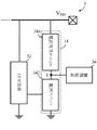
本発明による第1実施例はESD検出回路である。図3(A)を参照されたい。図3(A)は本発明の第1実施例におけるESD検出回路の基本構造を示す。図3(A)に示すように、ESD検出回路2はトリガ回路22、整流回路24、及び制御装置26を備える。整流回路24は整流ユニット242と電流制限ユニット244を備える。そして整流ユニット242と電流制限ユニット244は直列に接続される。
The first embodiment according to the present invention is an ESD detection circuit. Please refer to FIG. FIG. 3A shows the basic structure of the ESD detection circuit in the first embodiment of the present invention. As shown in FIG. 3A, the
実際の適用で、整流ユニット242はシリコン制御整流(SCR)装置を備え、電流制限ユニット244は少なくとも1つのMOSFET(金属酸化物半導体電界効果トランジスタ)装置を備える。例えば、電流制限ユニット244は、直列に接続される3つのNMOSを備えるNMOSスタックである。
In practical application, the rectifying
トリガ回路22は電源レール(VDD)とアースノード間に接続される。トリガ回路22がトランジェントノイズを受信すると、トリガ回路22はトリガ信号を発生させる。事実、トリガ回路22を使用してSCR装置のような整流ユニット242を起動することができる。そして、トリガ回路22は抵抗、キャパシタ、及びインバータを備える。更に、トリガ回路22は、抵抗、キャパシタ、及び直列に接続される複数のインバータを備えるインバータチェーンも備える。
The
図3(A)に示すように、整流回路24の整流ユニット242はトリガ回路22と電源レールへ接続される。整流ユニット242がトリガ回路22からトリガ信号を受信すると、整流ユニット242はトリガ信号により起動される。更に、整流回路24の電流制限ユニット244は整流ユニット242とアースノードへ接続される。電流制限ユニット244は提案された検出回路の全電力消費を制御することができる。
As shown in FIG. 3A, the rectifying
図3(A)に示すように、制御装置26は検出ノードDへ接続される。検出ノードDは整流ユニット242と電流制限ユニット244の間のノードである。制御装置26は検出ノードDの電圧を検出し、次に検出ノードDの電圧に基づきESD電圧レベルを決定する。
As shown in FIG. 3A, the
実際の適用で、もし制御装置26が決定するESD電圧レベルが異常に高いならば、制御装置26は、システム装置のより高い電磁互換(EMC)ロバスト性に対する内部回路を直ちに再起動又は再始動させることができる。従って、本発明によるESD検出回路2はシステム装置に対してノイズ検出機能を提供することができる。
In practical applications, if the ESD voltage level determined by the
図4(A)を参照されたい。図4(A)は図3(A)に示すESD検出回路の詳細図を示す。図4(A)に示すように、トリガ回路22はインバータINVと、直列に接続される抵抗Rと、キャパシタCを備えるRCユニットを備える。RCユニットは電源レールとアースノードへ接続される。インバータINVは電源レール、アースノード、整流ユニット242、及び抵抗RとキャパシタCの間のノードへ接続される。もしRCユニットが電源レールからトランジェントノイズを受信すると、RCユニットはRC遅延信号を発生させる。次に、インバータINVはRCユニットからRC遅延信号を受信し、そしてRC遅延信号に応じたトリガ信号を発生させる。
Please refer to FIG. FIG. 4A is a detailed diagram of the ESD detection circuit shown in FIG. As shown in FIG. 4A, the
実際の適用では、トリガ信号22はインバータユニットとRCユニットを備える。例えば、インバータチェーンは直列に接続される4つのインバータを備え、そしてRCユニットは直列に接続される抵抗Rと、キャパシタCを備える。事実、トリガ回路22の構造はこの実施例によって限定されない。それはトリガ回路22に対しなお他の可能な構造を有する。
In actual application, the
図4(A)に示すように、整流回路24の整流ユニット242はSCR装置であり、そして電流制限ユニット244はNMOS装置Mn1である。SCR装置242はトリガ回路22のインバータINVと電源レールへ接続される。NMOS装置Mn1と整流ユニット242は直列に接続され、そしてNMOS装置Mn1もアースノードへ接続される。トリガ信号がインバータINVにより発生された後、SCR装置242はインバータINVからトリガ信号を受信する。次に、SCR装置242はトリガ信号により起動される。
As shown in FIG. 4A, the rectifying
次に、図4(A)に示す制御装置26について論ずる。図4(A)に示すように、制御装置26は検出ノードDとNMOS装置Mn1のゲート端子へ接続される。検出ノードDはSCR装置242とNMOS装置Mn1の間のノードである。制御装置26は、検出ノードDの電圧を検出し、次に検出ノードDの電圧に基づき、ESD電圧レベルを決定するために使用される。
Next, the
更に、ESD検出回路2をリセットするため、制御装置26はリセット信号を発生させ、そしてリセットノードFを介してNMOS装置Mn1のゲート端子へリセット信号を伝送する。次に、NMOS装置Mn1はオフになり、SCR装置242を流れる電流はその保持電流(Ih)以下に低下する。そのため、SCR装置242は不充分な保持電流(Ih)のため、オフになる。その結果、ESD検出回路2はリセットされ、そして別のトランジェントノイズ事象の検出に備える。
Further, in order to reset the
実際の適用では、制御装置26は、更に続く回路に接続され、そして続く回路は制御装置26からESD電圧レベルを受信する。ESD電圧レベルに基づき、続く回路は対応する測定を実施し、そして柔軟なESD保護方針を提供することができる。
In actual application, the
本発明による第2実施例もESD検出回路である。図3(B)を参照されたい。図3(B)は本発明による第2実施例のESD検出回路の基本構造を示す。図3(B)に示すように、ESD検出回路3はトリガ回路32、整流回路34、及び制御装置36を備える。整流回路34は整流ユニット342と電流制限ユニット344を備える。そして、整流ユニット342と電流制限ユニット344は直列に接続される。
The second embodiment according to the present invention is also an ESD detection circuit. Please refer to FIG. FIG. 3B shows the basic structure of the ESD detection circuit according to the second embodiment of the present invention. As shown in FIG. 3B, the ESD detection circuit 3 includes a
実際の適用で、整流ユニット342はSCR装置を備え、そして電流制限ユニット344は少なくとも1つのMOSFET装置を備える。例えば、電流制限ユニット344は直列に接続される4つのPMOSを備えるPMOSスタックである。
In practical applications, the rectifying unit 342 comprises an SCR device and the current limiting
整流ユニット342はトリガ回路32とアースノードへ接続され、そして電流制限ユニット344は電源レール(VDD)と整流ユニット342へ接続されることは注目すべきである。制御装置36は検出ノードEへ接続される。検出ノードEは整流ユニット342と電流制限ユニット344の間のノードである。制御装置36は検出ノードEの電圧を検出し、次に検出ノードEの電圧に基づき、ESD電圧レベルを決定する。
It should be noted that the rectifying unit 342 is connected to the
図4(B)を参照されたい。図4(B)は図3(B)のESD検出回路の詳細図を示す。図4(B)に示すように、トリガ回路32はインバータINVと直列に接続される抵抗RとキャパシタCを備えるRCユニットを備える。RCユニットは電源レールとアースノードへ接続される。インバータINVは電源レール、アースノード、整流ユニット242、及び抵抗RとキャパシタCの間のノードへ接続される。もしRCユニットが電源レールからトランジェットノイズを受信すると、RCユニットはRC遅延信号を発生させる。次に、インバータINVはRCユニットからRC遅延信号を受信し、そしてRC遅延信号に応じてトリガ信号を発生させる。
Please refer to FIG. FIG. 4B is a detailed diagram of the ESD detection circuit of FIG. As shown in FIG. 4B, the
実際の適用で、トリガ回路32はインバータチェーンとRCユニットを備える。例えば、インバータチェーンは直列に接続される5つのインバータを備え、RCユニットは直列に接続される抵抗RとキャパシタCを備える。
In actual application, the
図4(B)に示すように、整流回路34の整流ユニット342はSCR装置であり、そして電流制限ユニット344はPMOS装置Mp1である。SCR装置342はトリガ回路32のインバータINVとアースノードへ接続される。PMOS装置MP1と整流ユニット342は直列に接続され、そしてPMOS装置Mp1も電源レールへ接続される。トリガ信号がインバータINVにより発生された後、SCR装置342はインバータINVからトリガ信号を受信する。次に、SCR装置342はトリガ信号により起動される。
As shown in FIG. 4B, the rectifying unit 342 of the rectifying
図4(B)に示すように、制御装置36は検出ノードEとPMOS装置Mp1のゲート端子へ接続される。検出ノードEはSCR装置342とPMOS装置Mp1の間のノードである。この実施例で、制御装置36は検出ノードEの電圧を検出し、次に検出ノードEの電圧に基づき、ESD電圧レベルを決定するために使用される。
As shown in FIG. 4B, the
実際の適用で、もし制御装置36が決定するESD電圧が異常であれば、制御装置36はシステム装置のより高いEMCロバスト性のため、内部回路を直ちに再起動又は再始動させることができる。従って、本発明によるESD検出回路3はシステム装置に対しノイズ検出機能を提供することができる。
In actual application, if the ESD voltage determined by the
要約すると、本発明によるトランジェントノイズ検出回路は、速いノイズトランジェント事象を検出するため、従来技術における受動装置に代わり、SCR装置と電流制限MOSFET装置を組み合わせることができる。従って、トランジェントノイズ検出回路はシステムへの寄生負荷による影響を防止することができる。 In summary, the transient noise detection circuit according to the present invention can combine an SCR device and a current limiting MOSFET device instead of a passive device in the prior art to detect fast noise transient events. Therefore, the transient noise detection circuit can prevent the influence of the parasitic load on the system.
更に、本発明によるトランジェントノイズ検出回路は、ESD事象の発生のみならず、ESD電圧レベルも検出することができる。ESD電圧レベルに基づき、続く回路は対応する測定を行うことができ、柔軟なESD保護方針を提供できる。更に、構造とその中のユニットは全く簡単であるので、本発明によるトランジェントノイズ検出回路を容易に実施することができる。 Furthermore, the transient noise detection circuit according to the present invention can detect not only the occurrence of an ESD event but also the ESD voltage level. Based on the ESD voltage level, subsequent circuitry can make corresponding measurements and provide a flexible ESD protection policy. Furthermore, since the structure and the units therein are quite simple, the transient noise detection circuit according to the present invention can be easily implemented.
上記例と説明で、本発明の特徴と精神を希望的によく記述する。当業者は、装置の多くの修正と変更は本発明の教示を維持しながら行われることが直ちに理解されるだろう。従って上記開示は付属の特許請求の範囲によってのみ限定されると解釈されるべきである。 In the above examples and description, the features and spirit of the invention are hopefully well described. Those skilled in the art will readily appreciate that many modifications and changes to the apparatus may be made while maintaining the teachings of the present invention. Accordingly, the above disclosure should be construed as limited only by the following claims.
2、16:ESD検出回路
3:検出回路
12:電源オン/リセット回路
14:内部回路
22、32:トリガ回路
24、34:整流回路
26、36:制御装置
242、342:整流ユニット
244、344:電流制限ユニット
2, 16: ESD detection circuit
3: Detection circuit
12: Power on / reset circuit
14: Internal circuit
22, 32: Trigger circuit
24, 34: Rectifier circuit
26, 36: Control device
242 and 342: Rectifier unit
244, 344: Current limiting unit
Claims (8)
前記トリガ回路から前記トリガ信号を受信すると、前記トリガ信号により起動され、直列に接続される整流ユニットと、電流制限ユニットを備え、前記トリガ回路、前記電源レール、および前記アースノードへ接続される整流回路;
前記検出ノードの電圧に基づき前記トランジェントノイズ電圧レベルを決定する、前記整流ユニットと前記電流制限ユニット間の検出ノードへ接続される制御装置;
を備えるトランジェントノイズ電圧レベルを検出するためのトランジェントノイズ検出回路。 A trigger circuit connected between the power rail and the ground node that generates a trigger signal when receiving transient noise;
Upon receiving the trigger signal from the trigger circuit, the rectifier is activated by the trigger signal and includes a rectification unit connected in series and a current limiting unit, and rectification connected to the trigger circuit, the power supply rail, and the ground node circuit;
A control device connected to a detection node between the rectifying unit and the current limiting unit for determining the transient noise voltage level based on the voltage of the detection node;
A transient noise detection circuit for detecting a transient noise voltage level.
前記電源レールと前記アースノードへ接続され、直列に接続される抵抗とキャパシタを備えるRCユニット;及び
前記電源レール、前記アースノード、前記整流ユニット、および前記RCユニットへ接続されるインバータ;を備え、
前記RCユニットが前記トランジェントノイズを受信すると、前記RCユニットはRC遅延信号を発生させ、次に前記インバータは前記RC遅延信号に応じて前記トリガ信号を発生させることを特徴とする、請求項1に記載のトランジェントノイズ検出回路。 The trigger circuit is:
An RC unit comprising a resistor and a capacitor connected in series and connected to the power rail and the earth node; and an inverter connected to the power rail, the earth node, the rectifier unit, and the RC unit;
The RC unit according to claim 1, wherein when the RC unit receives the transient noise, the RC unit generates an RC delay signal, and then the inverter generates the trigger signal in response to the RC delay signal. The transient noise detection circuit described.
前記電源レールと前記アースノードへ接続され、直列に接続される抵抗とキャパシタを備えるRCユニット;及び
前記電源レール、前記アースノード、前記整流ユニット、および前記RCユニットへ接続されるインバータチェーン;を備え、
前記RCユニットが前記トランジェントノイズを受信すると、前記RCユニットはRC遅延信号を発生させ、次に前記インバータはRC遅延信号に応じて前記トリガ信号を発生させることを特徴とする、請求項1に記載のトランジェントノイズ検出回路。 The trigger circuit is:
An RC unit connected to the power rail and the ground node and including a resistor and a capacitor connected in series; and an inverter chain connected to the power rail, the ground node, the rectifier unit, and the RC unit; ,
The RC unit according to claim 1, wherein when the RC unit receives the transient noise, the RC unit generates an RC delay signal, and then the inverter generates the trigger signal according to the RC delay signal. Transient noise detection circuit.
Applications Claiming Priority (2)
| Application Number | Priority Date | Filing Date | Title |
|---|---|---|---|
| US12/188,000 | 2008-08-07 | ||
| US12/188,000 US20100033164A1 (en) | 2008-08-07 | 2008-08-07 | Transient noise detection circuit |
Publications (2)
| Publication Number | Publication Date |
|---|---|
| JP2010041020A true JP2010041020A (en) | 2010-02-18 |
| JP5096282B2 JP5096282B2 (en) | 2012-12-12 |
Family
ID=41652308
Family Applications (1)
| Application Number | Title | Priority Date | Filing Date |
|---|---|---|---|
| JP2008262741A Active JP5096282B2 (en) | 2008-08-07 | 2008-10-09 | Transient noise detection circuit |
Country Status (3)
| Country | Link |
|---|---|
| US (1) | US20100033164A1 (en) |
| JP (1) | JP5096282B2 (en) |
| TW (1) | TW201012070A (en) |
Cited By (1)
| Publication number | Priority date | Publication date | Assignee | Title |
|---|---|---|---|---|
| JP2015537423A (en) * | 2012-10-04 | 2015-12-24 | クゥアルコム・インコーポレイテッドQualcomm Incorporated | ESD protection for class d power amplifiers |
Families Citing this family (2)
| Publication number | Priority date | Publication date | Assignee | Title |
|---|---|---|---|---|
| US8737028B2 (en) | 2011-12-06 | 2014-05-27 | International Business Machines Corporation | RC-triggered ESD clamp device with feedback for time constant adjustment |
| CN112067926B (en) * | 2020-09-08 | 2021-07-06 | 西安电子科技大学 | Circuit and method for detecting EFT interference resistance of MCU chip |
Citations (2)
| Publication number | Priority date | Publication date | Assignee | Title |
|---|---|---|---|---|
| JPH09297626A (en) * | 1996-03-07 | 1997-11-18 | Matsushita Electric Ind Co Ltd | Reference voltage source circuit and voltage feedback circuit |
| US20020122280A1 (en) * | 2001-03-05 | 2002-09-05 | Taiwan Semiconductor Manufacturing Co., Ltd. | SCR devices with deep-N-well structure for on-chip ESD protection circuits |
Family Cites Families (5)
| Publication number | Priority date | Publication date | Assignee | Title |
|---|---|---|---|---|
| KR100400383B1 (en) * | 1996-03-07 | 2003-12-31 | 마츠시타 덴끼 산교 가부시키가이샤 | Reference voltage source circuit and voltage feedback circuit |
| EP1368874B2 (en) * | 2001-03-16 | 2015-02-18 | Sofics BVBA | Electrostatic discharge protection structures for high speed technologies with mixed and ultra-low voltage supplies |
| US6573566B2 (en) * | 2001-07-09 | 2003-06-03 | United Microelectronics Corp. | Low-voltage-triggered SOI-SCR device and associated ESD protection circuit |
| US6521952B1 (en) * | 2001-10-22 | 2003-02-18 | United Microelectronics Corp. | Method of forming a silicon controlled rectifier devices in SOI CMOS process for on-chip ESD protection |
| US7102864B2 (en) * | 2004-06-14 | 2006-09-05 | King Billion Electronics Co., Ltd. | Latch-up-free ESD protection circuit using SCR |
-
2008
- 2008-08-07 US US12/188,000 patent/US20100033164A1/en not_active Abandoned
- 2008-09-12 TW TW097135226A patent/TW201012070A/en unknown
- 2008-10-09 JP JP2008262741A patent/JP5096282B2/en active Active
Patent Citations (2)
| Publication number | Priority date | Publication date | Assignee | Title |
|---|---|---|---|---|
| JPH09297626A (en) * | 1996-03-07 | 1997-11-18 | Matsushita Electric Ind Co Ltd | Reference voltage source circuit and voltage feedback circuit |
| US20020122280A1 (en) * | 2001-03-05 | 2002-09-05 | Taiwan Semiconductor Manufacturing Co., Ltd. | SCR devices with deep-N-well structure for on-chip ESD protection circuits |
Cited By (1)
| Publication number | Priority date | Publication date | Assignee | Title |
|---|---|---|---|---|
| JP2015537423A (en) * | 2012-10-04 | 2015-12-24 | クゥアルコム・インコーポレイテッドQualcomm Incorporated | ESD protection for class d power amplifiers |
Also Published As
| Publication number | Publication date |
|---|---|
| TW201012070A (en) | 2010-03-16 |
| US20100033164A1 (en) | 2010-02-11 |
| JP5096282B2 (en) | 2012-12-12 |
Similar Documents
| Publication | Publication Date | Title |
|---|---|---|
| US8116047B2 (en) | Electrostatic discharge protective circuit having rise time detector and discharge sustaining circuitry | |
| US8830640B2 (en) | Electrostatic discharge protection circuit | |
| US9843183B2 (en) | ESD protection circuit | |
| US8067952B2 (en) | System-level ESD detection circuit | |
| US20150245546A1 (en) | Electrostatic discharge protection circuit | |
| US6819539B1 (en) | Method for circuit recovery from overstress conditions | |
| US20150249334A1 (en) | Electrostatic discharge circuit with reduced standby current | |
| US20140092507A1 (en) | Mitigating cross-domain transmission of electrostatic discharge (esd) events | |
| TWI524495B (en) | Gate dielectric protection | |
| US20150049403A1 (en) | Bias-insensitive trigger circuit for bigfet esd supply protection | |
| US8570694B2 (en) | Low voltage electrostatic discharge protection | |
| US20070236842A1 (en) | Electrostatic discharge protection circuit | |
| US10158225B2 (en) | ESD protection system utilizing gate-floating scheme and control circuit thereof | |
| EP2919347B1 (en) | Surge-protection circuit and surge-protection method | |
| JP5096282B2 (en) | Transient noise detection circuit | |
| US20070242400A1 (en) | Device to protect semiconductor device from electrostatic discharge | |
| TWI495217B (en) | Esd protection circuit and electronic apparatus | |
| US20100118457A1 (en) | Electrostatic discharge protection circuit | |
| TWI487087B (en) | Electrostatic discharge protection apparatus | |
| JP2010183721A (en) | Ac power supply detecting circuit and dc power supply unit | |
| US20080074813A1 (en) | Discharge protection circuit | |
| US10079487B2 (en) | Clamp circuit for electrical overstress and electrostatic discharge | |
| TWI653797B (en) | Esd protected integrated circuit and esd detection circuit | |
| US20070252615A1 (en) | Logic-keeping apparatus for improving system-level electrostatic discharge robustness | |
| JP2010183724A (en) | Ac power supply detecting circuit and dc power supply unit |
Legal Events
| Date | Code | Title | Description |
|---|---|---|---|
| A977 | Report on retrieval |
Free format text: JAPANESE INTERMEDIATE CODE: A971007 Effective date: 20120309 |
|
| A131 | Notification of reasons for refusal |
Free format text: JAPANESE INTERMEDIATE CODE: A131 Effective date: 20120327 |
|
| A601 | Written request for extension of time |
Free format text: JAPANESE INTERMEDIATE CODE: A601 Effective date: 20120626 |
|
| A602 | Written permission of extension of time |
Free format text: JAPANESE INTERMEDIATE CODE: A602 Effective date: 20120629 |
|
| A521 | Request for written amendment filed |
Free format text: JAPANESE INTERMEDIATE CODE: A523 Effective date: 20120717 |
|
| TRDD | Decision of grant or rejection written | ||
| A01 | Written decision to grant a patent or to grant a registration (utility model) |
Free format text: JAPANESE INTERMEDIATE CODE: A01 Effective date: 20120821 |
|
| A01 | Written decision to grant a patent or to grant a registration (utility model) |
Free format text: JAPANESE INTERMEDIATE CODE: A01 |
|
| A61 | First payment of annual fees (during grant procedure) |
Free format text: JAPANESE INTERMEDIATE CODE: A61 Effective date: 20120920 |
|
| R150 | Certificate of patent or registration of utility model |
Ref document number: 5096282 Country of ref document: JP Free format text: JAPANESE INTERMEDIATE CODE: R150 Free format text: JAPANESE INTERMEDIATE CODE: R150 |
|
| FPAY | Renewal fee payment (event date is renewal date of database) |
Free format text: PAYMENT UNTIL: 20150928 Year of fee payment: 3 |
|
| R250 | Receipt of annual fees |
Free format text: JAPANESE INTERMEDIATE CODE: R250 |
|
| R250 | Receipt of annual fees |
Free format text: JAPANESE INTERMEDIATE CODE: R250 |
|
| R250 | Receipt of annual fees |
Free format text: JAPANESE INTERMEDIATE CODE: R250 |