JP2010037165A - Anodic joinable ceramic and composition for ceramic - Google Patents
Anodic joinable ceramic and composition for ceramic Download PDFInfo
- Publication number
- JP2010037165A JP2010037165A JP2008203425A JP2008203425A JP2010037165A JP 2010037165 A JP2010037165 A JP 2010037165A JP 2008203425 A JP2008203425 A JP 2008203425A JP 2008203425 A JP2008203425 A JP 2008203425A JP 2010037165 A JP2010037165 A JP 2010037165A
- Authority
- JP
- Japan
- Prior art keywords
- low
- temperature
- composition
- strength
- formula
- Prior art date
- Legal status (The legal status is an assumption and is not a legal conclusion. Google has not performed a legal analysis and makes no representation as to the accuracy of the status listed.)
- Granted
Links
- 239000000203 mixture Substances 0.000 title claims abstract description 62
- 239000000919 ceramic Substances 0.000 title claims abstract description 33
- 239000002131 composite material Substances 0.000 claims abstract description 19
- 229910001416 lithium ion Inorganic materials 0.000 claims abstract description 5
- 239000000758 substrate Substances 0.000 claims description 45
- 229910052710 silicon Inorganic materials 0.000 claims description 42
- 239000010703 silicon Substances 0.000 claims description 39
- XUIMIQQOPSSXEZ-UHFFFAOYSA-N Silicon Chemical compound [Si] XUIMIQQOPSSXEZ-UHFFFAOYSA-N 0.000 claims description 38
- 229910052573 porcelain Inorganic materials 0.000 claims description 35
- 229910004298 SiO 2 Inorganic materials 0.000 claims description 29
- 229910015902 Bi 2 O 3 Inorganic materials 0.000 claims description 17
- 229910018068 Li 2 O Inorganic materials 0.000 claims description 16
- 150000002500 ions Chemical class 0.000 claims description 14
- 229910018072 Al 2 O 3 Inorganic materials 0.000 claims description 12
- 239000011230 binding agent Substances 0.000 claims description 12
- 238000010304 firing Methods 0.000 claims description 11
- 150000002642 lithium compounds Chemical class 0.000 claims description 11
- 238000005452 bending Methods 0.000 claims description 10
- CNLWCVNCHLKFHK-UHFFFAOYSA-N aluminum;lithium;dioxido(oxo)silane Chemical compound [Li+].[Al+3].[O-][Si]([O-])=O.[O-][Si]([O-])=O CNLWCVNCHLKFHK-UHFFFAOYSA-N 0.000 claims description 9
- 150000002681 magnesium compounds Chemical class 0.000 claims description 8
- 229910052644 β-spodumene Inorganic materials 0.000 claims description 8
- 238000000465 moulding Methods 0.000 claims description 7
- XGZVUEUWXADBQD-UHFFFAOYSA-L lithium carbonate Chemical compound [Li+].[Li+].[O-]C([O-])=O XGZVUEUWXADBQD-UHFFFAOYSA-L 0.000 claims description 4
- 229910052808 lithium carbonate Inorganic materials 0.000 claims description 4
- ZLNQQNXFFQJAID-UHFFFAOYSA-L magnesium carbonate Chemical compound [Mg+2].[O-]C([O-])=O ZLNQQNXFFQJAID-UHFFFAOYSA-L 0.000 claims description 4
- 239000001095 magnesium carbonate Substances 0.000 claims description 4
- 229910000021 magnesium carbonate Inorganic materials 0.000 claims description 4
- 230000035515 penetration Effects 0.000 claims description 4
- VTHJTEIRLNZDEV-UHFFFAOYSA-L magnesium dihydroxide Chemical compound [OH-].[OH-].[Mg+2] VTHJTEIRLNZDEV-UHFFFAOYSA-L 0.000 claims description 3
- 239000000347 magnesium hydroxide Substances 0.000 claims description 3
- 229910001862 magnesium hydroxide Inorganic materials 0.000 claims description 3
- 238000005304 joining Methods 0.000 abstract description 3
- 239000013078 crystal Substances 0.000 description 43
- 239000012071 phase Substances 0.000 description 31
- 239000000463 material Substances 0.000 description 30
- 238000000034 method Methods 0.000 description 24
- 239000011521 glass Substances 0.000 description 22
- CPLXHLVBOLITMK-UHFFFAOYSA-N Magnesium oxide Chemical compound [Mg]=O CPLXHLVBOLITMK-UHFFFAOYSA-N 0.000 description 16
- 239000000843 powder Substances 0.000 description 15
- YXFVVABEGXRONW-UHFFFAOYSA-N Toluene Chemical compound CC1=CC=CC=C1 YXFVVABEGXRONW-UHFFFAOYSA-N 0.000 description 12
- 239000011734 sodium Substances 0.000 description 11
- DOIRQSBPFJWKBE-UHFFFAOYSA-N dibutyl phthalate Chemical compound CCCCOC(=O)C1=CC=CC=C1C(=O)OCCCC DOIRQSBPFJWKBE-UHFFFAOYSA-N 0.000 description 10
- 238000004519 manufacturing process Methods 0.000 description 9
- 238000012545 processing Methods 0.000 description 7
- 239000002994 raw material Substances 0.000 description 7
- 238000005245 sintering Methods 0.000 description 7
- ZWEHNKRNPOVVGH-UHFFFAOYSA-N 2-Butanone Chemical compound CCC(C)=O ZWEHNKRNPOVVGH-UHFFFAOYSA-N 0.000 description 6
- KFZMGEQAYNKOFK-UHFFFAOYSA-N Isopropanol Chemical compound CC(C)O KFZMGEQAYNKOFK-UHFFFAOYSA-N 0.000 description 6
- -1 borosilicate glass Chemical class 0.000 description 6
- 230000003746 surface roughness Effects 0.000 description 6
- 229910008556 Li2O—Al2O3—SiO2 Inorganic materials 0.000 description 5
- 239000004020 conductor Substances 0.000 description 5
- 238000007606 doctor blade method Methods 0.000 description 4
- 238000005553 drilling Methods 0.000 description 4
- 239000011777 magnesium Substances 0.000 description 4
- 229910052751 metal Inorganic materials 0.000 description 4
- 239000002184 metal Substances 0.000 description 4
- 239000002245 particle Substances 0.000 description 4
- 239000004014 plasticizer Substances 0.000 description 4
- 239000002002 slurry Substances 0.000 description 4
- 229910052782 aluminium Inorganic materials 0.000 description 3
- PNEYBMLMFCGWSK-UHFFFAOYSA-N aluminium oxide Inorganic materials [O-2].[O-2].[O-2].[Al+3].[Al+3] PNEYBMLMFCGWSK-UHFFFAOYSA-N 0.000 description 3
- 239000005388 borosilicate glass Substances 0.000 description 3
- 238000001354 calcination Methods 0.000 description 3
- 229910052878 cordierite Inorganic materials 0.000 description 3
- 238000013461 design Methods 0.000 description 3
- JSKIRARMQDRGJZ-UHFFFAOYSA-N dimagnesium dioxido-bis[(1-oxido-3-oxo-2,4,6,8,9-pentaoxa-1,3-disila-5,7-dialuminabicyclo[3.3.1]nonan-7-yl)oxy]silane Chemical compound [Mg++].[Mg++].[O-][Si]([O-])(O[Al]1O[Al]2O[Si](=O)O[Si]([O-])(O1)O2)O[Al]1O[Al]2O[Si](=O)O[Si]([O-])(O1)O2 JSKIRARMQDRGJZ-UHFFFAOYSA-N 0.000 description 3
- 238000010438 heat treatment Methods 0.000 description 3
- 239000007791 liquid phase Substances 0.000 description 3
- 229910052744 lithium Inorganic materials 0.000 description 3
- 229910052749 magnesium Inorganic materials 0.000 description 3
- 238000005498 polishing Methods 0.000 description 3
- 229910001218 Gallium arsenide Inorganic materials 0.000 description 2
- DGAQECJNVWCQMB-PUAWFVPOSA-M Ilexoside XXIX Chemical compound C[C@@H]1CC[C@@]2(CC[C@@]3(C(=CC[C@H]4[C@]3(CC[C@@H]5[C@@]4(CC[C@@H](C5(C)C)OS(=O)(=O)[O-])C)C)[C@@H]2[C@]1(C)O)C)C(=O)O[C@H]6[C@@H]([C@H]([C@@H]([C@H](O6)CO)O)O)O.[Na+] DGAQECJNVWCQMB-PUAWFVPOSA-M 0.000 description 2
- 239000004372 Polyvinyl alcohol Substances 0.000 description 2
- VYPSYNLAJGMNEJ-UHFFFAOYSA-N Silicium dioxide Chemical compound O=[Si]=O VYPSYNLAJGMNEJ-UHFFFAOYSA-N 0.000 description 2
- 229910052783 alkali metal Inorganic materials 0.000 description 2
- 229910001413 alkali metal ion Inorganic materials 0.000 description 2
- 150000001340 alkali metals Chemical class 0.000 description 2
- 238000005219 brazing Methods 0.000 description 2
- 239000003990 capacitor Substances 0.000 description 2
- 238000006243 chemical reaction Methods 0.000 description 2
- 230000000052 comparative effect Effects 0.000 description 2
- 239000000470 constituent Substances 0.000 description 2
- 238000007796 conventional method Methods 0.000 description 2
- 238000009713 electroplating Methods 0.000 description 2
- 238000011049 filling Methods 0.000 description 2
- XLYOFNOQVPJJNP-UHFFFAOYSA-M hydroxide Chemical compound [OH-] XLYOFNOQVPJJNP-UHFFFAOYSA-M 0.000 description 2
- 239000011812 mixed powder Substances 0.000 description 2
- 230000001590 oxidative effect Effects 0.000 description 2
- 229910052760 oxygen Inorganic materials 0.000 description 2
- 238000004806 packaging method and process Methods 0.000 description 2
- 229920002451 polyvinyl alcohol Polymers 0.000 description 2
- 238000010298 pulverizing process Methods 0.000 description 2
- 238000012827 research and development Methods 0.000 description 2
- 229910052708 sodium Inorganic materials 0.000 description 2
- 229910000679 solder Inorganic materials 0.000 description 2
- 239000002904 solvent Substances 0.000 description 2
- 229910052719 titanium Inorganic materials 0.000 description 2
- RZVAJINKPMORJF-UHFFFAOYSA-N Acetaminophen Chemical compound CC(=O)NC1=CC=C(O)C=C1 RZVAJINKPMORJF-UHFFFAOYSA-N 0.000 description 1
- QTBSBXVTEAMEQO-UHFFFAOYSA-M Acetate Chemical compound CC([O-])=O QTBSBXVTEAMEQO-UHFFFAOYSA-M 0.000 description 1
- 239000004925 Acrylic resin Substances 0.000 description 1
- 229920000178 Acrylic resin Polymers 0.000 description 1
- 238000007088 Archimedes method Methods 0.000 description 1
- BVKZGUZCCUSVTD-UHFFFAOYSA-L Carbonate Chemical compound [O-]C([O-])=O BVKZGUZCCUSVTD-UHFFFAOYSA-L 0.000 description 1
- FYYHWMGAXLPEAU-UHFFFAOYSA-N Magnesium Chemical compound [Mg] FYYHWMGAXLPEAU-UHFFFAOYSA-N 0.000 description 1
- 229910002651 NO3 Inorganic materials 0.000 description 1
- NHNBFGGVMKEFGY-UHFFFAOYSA-N Nitrate Chemical compound [O-][N+]([O-])=O NHNBFGGVMKEFGY-UHFFFAOYSA-N 0.000 description 1
- 238000010521 absorption reaction Methods 0.000 description 1
- 230000001133 acceleration Effects 0.000 description 1
- 230000004913 activation Effects 0.000 description 1
- 239000000654 additive Substances 0.000 description 1
- 230000000996 additive effect Effects 0.000 description 1
- 239000000853 adhesive Substances 0.000 description 1
- 230000001070 adhesive effect Effects 0.000 description 1
- 230000015572 biosynthetic process Effects 0.000 description 1
- 229910010293 ceramic material Inorganic materials 0.000 description 1
- 238000004891 communication Methods 0.000 description 1
- 238000012790 confirmation Methods 0.000 description 1
- 229910052802 copper Inorganic materials 0.000 description 1
- 239000011162 core material Substances 0.000 description 1
- 230000007812 deficiency Effects 0.000 description 1
- 230000032798 delamination Effects 0.000 description 1
- 238000000280 densification Methods 0.000 description 1
- 238000001514 detection method Methods 0.000 description 1
- 238000009792 diffusion process Methods 0.000 description 1
- 239000002270 dispersing agent Substances 0.000 description 1
- 230000000694 effects Effects 0.000 description 1
- 238000004070 electrodeposition Methods 0.000 description 1
- 238000005516 engineering process Methods 0.000 description 1
- 230000005496 eutectics Effects 0.000 description 1
- 238000001125 extrusion Methods 0.000 description 1
- 239000002241 glass-ceramic Substances 0.000 description 1
- 229910052737 gold Inorganic materials 0.000 description 1
- 238000003780 insertion Methods 0.000 description 1
- 230000037431 insertion Effects 0.000 description 1
- 238000007689 inspection Methods 0.000 description 1
- 238000009413 insulation Methods 0.000 description 1
- 238000011835 investigation Methods 0.000 description 1
- 229910052742 iron Inorganic materials 0.000 description 1
- 239000007788 liquid Substances 0.000 description 1
- 238000005259 measurement Methods 0.000 description 1
- 238000002844 melting Methods 0.000 description 1
- 230000008018 melting Effects 0.000 description 1
- 229910044991 metal oxide Inorganic materials 0.000 description 1
- 150000004706 metal oxides Chemical class 0.000 description 1
- 238000001465 metallisation Methods 0.000 description 1
- 150000002739 metals Chemical class 0.000 description 1
- 238000002156 mixing Methods 0.000 description 1
- 239000003960 organic solvent Substances 0.000 description 1
- 230000003647 oxidation Effects 0.000 description 1
- 238000007254 oxidation reaction Methods 0.000 description 1
- 239000001301 oxygen Substances 0.000 description 1
- 230000000704 physical effect Effects 0.000 description 1
- 238000013001 point bending Methods 0.000 description 1
- 229920001225 polyester resin Polymers 0.000 description 1
- 239000004645 polyester resin Substances 0.000 description 1
- 230000001376 precipitating effect Effects 0.000 description 1
- 238000004080 punching Methods 0.000 description 1
- 239000005297 pyrex Substances 0.000 description 1
- 238000001953 recrystallisation Methods 0.000 description 1
- 238000005096 rolling process Methods 0.000 description 1
- 150000003839 salts Chemical class 0.000 description 1
- 238000005488 sandblasting Methods 0.000 description 1
- 238000007650 screen-printing Methods 0.000 description 1
- 229910052709 silver Inorganic materials 0.000 description 1
- 229910001415 sodium ion Inorganic materials 0.000 description 1
- 239000007790 solid phase Substances 0.000 description 1
- 229910052642 spodumene Inorganic materials 0.000 description 1
- 239000007858 starting material Substances 0.000 description 1
- 239000000126 substance Substances 0.000 description 1
- 230000008646 thermal stress Effects 0.000 description 1
- XLYOFNOQVPJJNP-UHFFFAOYSA-N water Substances O XLYOFNOQVPJJNP-UHFFFAOYSA-N 0.000 description 1
Images
Classifications
-
- H—ELECTRICITY
- H05—ELECTRIC TECHNIQUES NOT OTHERWISE PROVIDED FOR
- H05K—PRINTED CIRCUITS; CASINGS OR CONSTRUCTIONAL DETAILS OF ELECTRIC APPARATUS; MANUFACTURE OF ASSEMBLAGES OF ELECTRICAL COMPONENTS
- H05K1/00—Printed circuits
- H05K1/02—Details
- H05K1/03—Use of materials for the substrate
- H05K1/0306—Inorganic insulating substrates, e.g. ceramic, glass
-
- B—PERFORMING OPERATIONS; TRANSPORTING
- B81—MICROSTRUCTURAL TECHNOLOGY
- B81C—PROCESSES OR APPARATUS SPECIALLY ADAPTED FOR THE MANUFACTURE OR TREATMENT OF MICROSTRUCTURAL DEVICES OR SYSTEMS
- B81C1/00—Manufacture or treatment of devices or systems in or on a substrate
- B81C1/00015—Manufacture or treatment of devices or systems in or on a substrate for manufacturing microsystems
- B81C1/00261—Processes for packaging MEMS devices
- B81C1/00269—Bonding of solid lids or wafers to the substrate
-
- C—CHEMISTRY; METALLURGY
- C04—CEMENTS; CONCRETE; ARTIFICIAL STONE; CERAMICS; REFRACTORIES
- C04B—LIME, MAGNESIA; SLAG; CEMENTS; COMPOSITIONS THEREOF, e.g. MORTARS, CONCRETE OR LIKE BUILDING MATERIALS; ARTIFICIAL STONE; CERAMICS; REFRACTORIES; TREATMENT OF NATURAL STONE
- C04B35/00—Shaped ceramic products characterised by their composition; Ceramics compositions; Processing powders of inorganic compounds preparatory to the manufacturing of ceramic products
- C04B35/01—Shaped ceramic products characterised by their composition; Ceramics compositions; Processing powders of inorganic compounds preparatory to the manufacturing of ceramic products based on oxide ceramics
- C04B35/16—Shaped ceramic products characterised by their composition; Ceramics compositions; Processing powders of inorganic compounds preparatory to the manufacturing of ceramic products based on oxide ceramics based on silicates other than clay
- C04B35/18—Shaped ceramic products characterised by their composition; Ceramics compositions; Processing powders of inorganic compounds preparatory to the manufacturing of ceramic products based on oxide ceramics based on silicates other than clay rich in aluminium oxide
- C04B35/19—Alkali metal aluminosilicates, e.g. spodumene
-
- B—PERFORMING OPERATIONS; TRANSPORTING
- B81—MICROSTRUCTURAL TECHNOLOGY
- B81C—PROCESSES OR APPARATUS SPECIALLY ADAPTED FOR THE MANUFACTURE OR TREATMENT OF MICROSTRUCTURAL DEVICES OR SYSTEMS
- B81C2203/00—Forming microstructural systems
- B81C2203/01—Packaging MEMS
- B81C2203/0118—Bonding a wafer on the substrate, i.e. where the cap consists of another wafer
-
- H—ELECTRICITY
- H01—ELECTRIC ELEMENTS
- H01L—SEMICONDUCTOR DEVICES NOT COVERED BY CLASS H10
- H01L23/00—Details of semiconductor or other solid state devices
- H01L23/12—Mountings, e.g. non-detachable insulating substrates
- H01L23/14—Mountings, e.g. non-detachable insulating substrates characterised by the material or its electrical properties
- H01L23/15—Ceramic or glass substrates
-
- H—ELECTRICITY
- H01—ELECTRIC ELEMENTS
- H01L—SEMICONDUCTOR DEVICES NOT COVERED BY CLASS H10
- H01L2924/00—Indexing scheme for arrangements or methods for connecting or disconnecting semiconductor or solid-state bodies as covered by H01L24/00
- H01L2924/0001—Technical content checked by a classifier
- H01L2924/0002—Not covered by any one of groups H01L24/00, H01L24/00 and H01L2224/00
-
- Y—GENERAL TAGGING OF NEW TECHNOLOGICAL DEVELOPMENTS; GENERAL TAGGING OF CROSS-SECTIONAL TECHNOLOGIES SPANNING OVER SEVERAL SECTIONS OF THE IPC; TECHNICAL SUBJECTS COVERED BY FORMER USPC CROSS-REFERENCE ART COLLECTIONS [XRACs] AND DIGESTS
- Y10—TECHNICAL SUBJECTS COVERED BY FORMER USPC
- Y10T—TECHNICAL SUBJECTS COVERED BY FORMER US CLASSIFICATION
- Y10T428/00—Stock material or miscellaneous articles
- Y10T428/24—Structurally defined web or sheet [e.g., overall dimension, etc.]
- Y10T428/24802—Discontinuous or differential coating, impregnation or bond [e.g., artwork, printing, retouched photograph, etc.]
- Y10T428/24926—Discontinuous or differential coating, impregnation or bond [e.g., artwork, printing, retouched photograph, etc.] including ceramic, glass, porcelain or quartz layer
Landscapes
- Engineering & Computer Science (AREA)
- Chemical & Material Sciences (AREA)
- Microelectronics & Electronic Packaging (AREA)
- Manufacturing & Machinery (AREA)
- Ceramic Engineering (AREA)
- Materials Engineering (AREA)
- Structural Engineering (AREA)
- Organic Chemistry (AREA)
- Inorganic Chemistry (AREA)
- Compositions Of Oxide Ceramics (AREA)
Abstract
Description
本発明は、陽極接合可能な、低温焼成高強度低熱膨張性磁器及び前記磁器用組成物に関する。さらに詳しく言えば、前記組成物を成形及び焼結してなる配線基板、好ましくは、MEMS(Micro Electro Mechanical Systems)の気密封止貫通配線基板として適している焼結基板、及びこの気密封止貫通配線基板を用いウエハレベルパッケージングしてなるMEMS(Micro Electro Mechanical Systems)素子に関する。 The present invention relates to a low-temperature fired high-strength low-temperature-expandable porcelain capable of anodic bonding and the porcelain composition. More specifically, a wiring board formed by molding and sintering the composition, preferably a sintered board suitable as a hermetically sealed through wiring board for MEMS (Micro Electro Mechanical Systems), and the hermetically sealed penetration. The present invention relates to a MEMS (Micro Electro Mechanical Systems) element formed by wafer level packaging using a wiring board.
陽極接合は、ホウケイ酸ガラスに代表されるようなアルカリ金属を含むガラスとシリコンを接触させた状態で、ガラス中のナトリウムなどのアルカリ金属イオンが動き易い温度まで加熱し、シリコン側を正、ガラス側を負の電極に接続して数百〜千ボルト程度の直流電圧を印加することにより、ガラスとシリコンを接合する方法である。アルカリ金属イオンが負極側に移動した際に生じる非架橋酸素イオンとシリコンが静電的に引き合い、ガラス−シリコン界面で化学結合を生じることにより、強固で信頼性の高い接合が得られ、圧力センサや加速度センサなどの実装技術として多用されている。 In anodic bonding, glass containing alkali metal, such as borosilicate glass, is in contact with silicon and heated to a temperature at which alkali metal ions such as sodium in the glass can easily move. This is a method of joining glass and silicon by connecting a side to a negative electrode and applying a DC voltage of about several hundred to 1,000 volts. Non-bridging oxygen ions generated when alkali metal ions move to the negative electrode side and silicon are electrostatically attracted to form a chemical bond at the glass-silicon interface, resulting in a strong and reliable bond, and a pressure sensor It is often used as a mounting technology for sensors and acceleration sensors.
MEMSは、研究開発段階を過ぎ、自動車、ゲーム機器などのセンサに使用され、実用化、普及化の段階に入ってきている。携帯電話などの通信機器に搭載されるようにするためには、低コスト化とともに、小型・低背・高機能化が重要と言われている。現状、MEMSのコストにおいて、約80%がパッケージを用いた実装と検査コストの費用と言われており、小型・低背・高機能化においても、このパッケージ実装が大きなネックとなっている。 MEMS has passed the research and development stage, has been used in sensors for automobiles, game machines, etc., and has entered the stage of practical use and diffusion. In order to be installed in communication devices such as mobile phones, it is said that not only cost reduction but also small size, low profile and high functionality are important. At present, about 80% of the cost of MEMS is said to be the cost of mounting and inspection cost using a package, and this package mounting is a major bottleneck in miniaturization, low profile and high functionality.
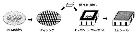
現在、使用されているMEMSは、図1のようなパッケージに実装されており製造プロセスは以下のとおりである。
1)ウエハ状態で製造されたMEMS素子をダイシングしチップ(個片)化させる。
2)ウエハからチップを取り出し、パッケージ基板に結合材を介して取り付け、MEMSチップの電極とパッケージの電極を金属ワイヤーで接続させる。
3)MEMSチップは可動部をもつためパッケージに蓋をして気密封止する。
パッケージ実装による製造方法は、このように多くの工程があるだけでなく、可動部のあるMEMSチップを工程中に保護なしで取り扱うため壊れやすく歩留まり低下の原因にもなっている。また、チップに比べパッケージは大きく、これが小型・低背化の大きな阻害要因ともなっている。
Currently used MEMS is mounted in a package as shown in FIG. 1, and the manufacturing process is as follows.
1) A MEMS element manufactured in a wafer state is diced into chips.
2) The chip is taken out from the wafer and attached to the package substrate via a bonding material, and the electrode of the MEMS chip and the electrode of the package are connected by a metal wire.
3) Since the MEMS chip has a movable part, the package is covered and hermetically sealed.
The manufacturing method by package mounting not only has many processes as described above, but also handles a MEMS chip having a movable part without protection during the process, which is fragile and causes a decrease in yield. In addition, the package is larger than the chip, and this is a major impediment to downsizing and low profile.
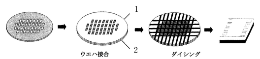
この解決策としてウエハレベル実装が開発されており、この実装方法は図2のようなプロセスで構成されている。MEMS素子が形成されたシリコンウエハと実装基板を直接貼り合わせ気密封止出来れば、組立プロセスが大幅に簡略化され、歩留まり低下の大きな要因であった可動部をもつチップでのハンドリングがなくなるだけでなく、MEMSの小型および低背化が可能となる。また1ウエハでとれるチップ数が増大しコスト低減に大きな効果をもたらす。このウエハレベル実装を実現するためには、気密封止されたMEMSチップから外部へ信号を取り出すための貫通配線実装基板が必要である。MEMSデバイスの電極と接合した実装基板側の電極を裏面に取り出す必要があるからである。この貫通配線基板材料としてガラスやシリコンに貫通孔をあけ導体材料を埋めたものが使われている。 Wafer level mounting has been developed as a solution to this problem, and this mounting method includes a process as shown in FIG. If the silicon wafer on which the MEMS element is formed and the mounting substrate can be directly bonded and hermetically sealed, the assembly process can be greatly simplified and handling with a chip having a movable part, which has been a major factor in yield reduction, can be eliminated. In addition, the MEMS can be reduced in size and height. In addition, the number of chips that can be taken with one wafer increases, which brings about a significant effect on cost reduction. In order to realize this wafer level mounting, a through wiring mounting substrate for taking out a signal from the hermetically sealed MEMS chip to the outside is necessary. This is because it is necessary to take out the electrode on the mounting substrate side bonded to the electrode of the MEMS device to the back surface. As the through wiring board material, a glass or silicon having a through hole and filled with a conductive material is used.
ガラスへの孔加工として用いられているドリル加工は孔形状はよいものの孔サイズとピッチの微細化に限界があり、またウエハ中の穴数が増えると削れなくなるために孔数に限界がある。またサンドブラスト加工は一度に多くの孔加工が同時にできるものの孔形状が悪く孔サイズやピッチにも限界がある。孔加工後貫通配線処理を行うことになるが、複雑な工程が必要である。実用化されている例では孔側面の金属化処理、導電用金属芯材の挿入、ロウ材の流し込み、鏡面研磨の順で仕上げられる。コストが高く微細化・大口径化に限界がある。 Although the drilling used for drilling glass has a good hole shape, there is a limit to the refinement of the hole size and pitch, and there is a limit to the number of holes because the number of holes in the wafer cannot be reduced. In addition, although sand blasting can simultaneously process many holes at the same time, the hole shape is poor and the hole size and pitch are limited. Although through wiring processing is performed after drilling, a complicated process is required. In an example that is put into practical use, finishing is performed in the order of metallization treatment of the hole side surface, insertion of a conductive metal core material, pouring of a brazing material, and mirror polishing. Cost is high and there is a limit to miniaturization and large diameter.
シリコンはDeep RIE装置を用いて微細な孔加工が可能であるが、Deep RIE装置は非常に高価で処理時間もかかる。孔加工後ガラスと同様複雑な工程で貫通配線基板が作られている。絶縁のための酸化処理、電気めっき用のシード層形成、電気めっきによる穴埋め、鏡面研磨の順で仕上げられる。また陽極接合できないのでプラズマ金属活性化法や常温接合などでシリコンMEMSウエハと接合されるが、接合装置がかなり高価で接合処理時間もかかる。微細な基板が作れるが、設備投資が相当必要でコストも高い点が課題である。 Silicon can be drilled with a deep RIE apparatus, but the Deep RIE apparatus is very expensive and takes a long processing time. Through-hole wiring boards are made in the same complicated process as glass after hole processing. It is finished in the order of oxidation treatment for insulation, seed layer formation for electroplating, hole filling by electroplating, and mirror polishing. In addition, since anodic bonding cannot be performed, the silicon MEMS wafer is bonded to the silicon MEMS wafer by plasma metal activation or room temperature bonding. However, the bonding apparatus is quite expensive and takes a long time for bonding. Although a fine substrate can be made, the problem is that it requires considerable capital investment and the cost is high.
このように、これまでウエハレベル実装基板材料としてはガラスやシリコンを用いた材料が検討されてきているが、これらの材料では貫通配線を形成する工程が複雑でそのコストも高く、また多層配線できないため設計に自由度がないことが課題となっている。 As described above, materials using glass or silicon have been studied as wafer level mounting substrate materials so far, but these materials require a complicated process for forming through wiring, and the cost thereof is high, and multilayer wiring cannot be performed. Therefore, the problem is that there is no freedom in design.
多層配線基板として、低温同時焼成セラミックス(LTCC)基板が広く知られている。LTCC(Low Temperature Co-fired Ceramics)は、携帯電話や車載用途の高周波部品やモジュール基板などで数多く使用されているセラミック多層基板である。貫通配線や多層配線を低コストで量産性よく製造できる基板であり、また基板内にコンデンサやコイルなどの受動部品も内蔵することが可能である。 As a multilayer wiring board, a low temperature co-fired ceramic (LTCC) substrate is widely known. LTCC (Low Temperature Co-fired Ceramics) is a ceramic multilayer substrate that is widely used in high-frequency components and module substrates for mobile phones and in-vehicle use. It is a substrate that can manufacture through wiring and multilayer wiring at low cost with high productivity, and can also incorporate passive components such as capacitors and coils in the substrate.
LTCC基板は、一般には、セラミックス材料にガラス等を加えた混合材料に有機バインダーを加えてシート化したグリーンシートを用い、そのシートに上下に接続するための貫通孔を開け、導体を含んだペーストを貫通孔の中およびグリーンシート表面に印刷し、ついでこれらのグリーンシートを正確に積み重ね、加熱加圧により積層して一体化した後、焼成することにより製造される。 The LTCC substrate is generally a paste containing a conductor using a green sheet made by adding an organic binder to a mixed material in which glass or the like is added to a ceramic material, and through-holes are formed in the sheet to connect up and down. Are printed in the through holes and on the surface of the green sheet, and then these green sheets are accurately stacked, laminated by heating and pressurizing, and then fired.
LTCC基板への孔あけはグリーンシートにパンチピンもしくはレーザー加工により行なうことができるため容易で量産性も高い。また孔あけされたグリーンシートへの導体充填も汎用技術であるスクリーン印刷で容易に行うことができる。
ガラスやシリコンでは多層配線が困難であるが、LTCC基板はグリーンシートを何枚も積み重ねて製造するので容易に多層基板とすることができる。内層で再配線設計が可能なのでMEMSチップ側の電極パッド位置と2次実装側の電極パッドの位置を気にする必要がなく配線設計の自由度が上がる。必要があればLTCC基板でよく用いられているようにコンデンサやコイルなどの受動部品を内蔵させて高機能化させることも可能である。
このようにLTCC基板は現在使われているMEMS貫通配線電極基板材料であるガラスやシリコンと比べると製造が容易でコストも低減できると考えられる。
しかし、熱膨張係数がシリコンと整合していなかったり、シリコンとの接合方法が半田、ロウ材、ガラス、有機系接着剤など介在物を用いる方法しかないためウエハと接合させる際の信頼性の観点で採用が難しかった。
Since drilling in the LTCC substrate can be performed on the green sheet by punch pins or laser processing, it is easy and has high mass productivity. Also, conductor filling into the perforated green sheet can be easily performed by screen printing, which is a general-purpose technique.
Although multilayer wiring is difficult with glass or silicon, the LTCC substrate is manufactured by stacking a number of green sheets, so that it can be easily formed into a multilayer substrate. Since rewiring design is possible in the inner layer, there is no need to worry about the position of the electrode pad on the MEMS chip side and the position of the electrode pad on the secondary mounting side, and the degree of freedom in wiring design is increased. If necessary, it is possible to increase the functionality by incorporating passive components such as capacitors and coils, as is often used in LTCC substrates.
Thus, it is considered that the LTCC substrate is easy to manufacture and can be reduced in cost as compared with glass and silicon, which are currently used MEMS through wiring electrode substrate materials.
However, the thermal expansion coefficient does not match that of silicon, or the only bonding method with silicon is the use of inclusions such as solder, brazing material, glass, organic adhesive, etc. It was difficult to adopt.
LTCCをMEMSウエハレベル実装用基板として用いるためには、これまでのLTCCでは出来なかった接合技術が適用できる材料を開発する必要があり、それが陽極接合である。陽極接合はシリコンとガラス基板で作られた実装基板との接合方法として用いられている方法で、この方法は製造設備が簡便であり、接合歩留まりも良く、また信頼性も高い。LTCCと他の材料との接合はAu/Sn共晶半田などの接着能力をもつ材料を利用した方法がほとんどで、陽極接合に関しては近年ドイツでナトリウムを伝導イオンとして陽極接合できる材料の発表があっただけである(特許文献1)。 In order to use LTCC as a substrate for MEMS wafer level mounting, it is necessary to develop a material to which a bonding technique that has not been possible with conventional LTCC can be applied, which is anodic bonding. Anodic bonding is a method used as a bonding method between a mounting substrate made of silicon and a glass substrate. This method has simple manufacturing equipment, good bonding yield, and high reliability. In most cases, LTCC and other materials are bonded using a material having bonding ability, such as Au / Sn eutectic solder, and anodic bonding has recently been announced in Germany regarding materials that can be anodic bonded using sodium as a conductive ion. (Patent Document 1).
特許文献1にはシリコンと陽極接合可能なガラスセラミック(LTCC)、具体的には、アルカリ金属を含むガラス粉末とアルミナとコージェライト及び/またはシリカガラスとからなるセラミック粉末を用いた低温焼結セラミックスが記載されている。ガラス粉末としては2.6wt%程度のNa成分を含む硼珪酸ガラスを用いており、熱膨張係数はシリコンとほぼ同等な3.4ppm/℃であるとしている。組成は硼珪酸ガラス:60〜70wt%、アルミナ:10〜20wt%、コーディエライトもしくはシリカガラス:8〜25wt%でありNa成分の含有量は1.5wt%以上である。 Patent Document 1 discloses a glass ceramic (LTCC) capable of anodic bonding with silicon, specifically, a low-temperature sintered ceramic using a glass powder containing an alkali metal and a ceramic powder made of alumina, cordierite and / or silica glass. Is described. As the glass powder, borosilicate glass containing Na component of about 2.6 wt% is used, and the thermal expansion coefficient is 3.4 ppm / ° C., which is almost the same as that of silicon. The composition is borosilicate glass: 60 to 70 wt%, alumina: 10 to 20 wt%, cordierite or silica glass: 8 to 25 wt%, and the content of Na component is 1.5 wt% or more.
シリコンと接合させる際には加熱処理が必要であるため、シリコンと近似した熱膨張係数の材料でないと熱ストレスによってMEMSウエハと実装基板の電極位置がずれる可能性があるが、これまでLTCCでは、シリコンの熱膨張係数に近い材料は特殊用途のみでしか開発されていない。本発明者らが従来提供したLTCC材料は、熱膨張係数が5.5ppm/℃で、HTCC ( High Temperature Co-fired Ceramics)の7ppm/℃よりは小さいが、MEMS用ウエハレベル実装基板に用いるには十分な値ではなかった。本発明者らは、さらに研究開発を進め、2007年に陽極接合可能でシリコンと熱膨張係数が近いLTCCを新たに提供した。 Since heat treatment is required when bonding to silicon, the electrode position of the MEMS wafer and the mounting substrate may shift due to thermal stress unless the material has a thermal expansion coefficient approximate to that of silicon. Materials close to the thermal expansion coefficient of silicon have been developed only for special applications. The LTCC material conventionally provided by the present inventors has a thermal expansion coefficient of 5.5 ppm / ° C., which is smaller than 7 ppm / ° C. of HTCC (High Temperature Co-fired Ceramics), but is used for a wafer level mounting substrate for MEMS. Was not enough. The present inventors further advanced research and development, and in 2007 newly provided LTCC that can be anodically bonded and has a thermal expansion coefficient close to that of silicon.
この材料は、Na2O−Al2O3−B2O3−SiO2系のガラスとセラミック粉末から組成されたもので、熱膨張係数はシリコンとほとんど同じ3.3ppm/℃に調整されている。また、Naを陽極接合時の伝導イオンとしており、設定温度400℃、600VDC印加の条件で接合できていることも確認した。この基板で試作や調査を行う中で以下の知見(a)〜(b)を得た。
(a)MEMSに与える影響が少ないため、低い陽極接合温度が要望されている。この低温化は、陽極接合時の伝導イオンを、Naから、よりイオン半径の小さいLiに変えることで実現出来ることが判った。
(b)試作の中で、薄い大口径基板は割れ易くハンドリング性に不安があり、高強度の材料が必要であることが判った。
This material is composed of Na 2 O—Al 2 O 3 —B 2 O 3 —SiO 2 glass and ceramic powder, and its thermal expansion coefficient is adjusted to 3.3 ppm / ° C., which is almost the same as that of silicon. Yes. It was also confirmed that Na was used as a conductive ion at the time of anodic bonding, and that bonding was possible under the conditions of a preset temperature of 400 ° C. and 600 VDC. The following findings (a) to (b) were obtained during trial manufacture and investigation on this substrate.
(A) Since there is little influence on MEMS, a low anodic bonding temperature is desired. It has been found that this low temperature can be realized by changing the conductive ions at the time of anodic bonding from Na to Li having a smaller ion radius.
(B) In the trial production, it was found that a thin large-diameter substrate is easily broken and has an uneasy handling property and requires a high-strength material.
従って、本発明は以上の知見(a)〜(b)に基づくものであり、その目的は、低温で陽極接合でき、従来の低熱膨張性LTCCよりも高い抗折強度を有するLTCCを提供することにある。 Accordingly, the present invention is based on the above findings (a) to (b), and an object thereof is to provide an LTCC that can be anodically bonded at a low temperature and has a bending strength higher than that of a conventional low thermal expansion LTCC. It is in.
すなわち、本発明は、低温で陽極接合可能な、低温焼成高強度低熱膨張性磁器及び前記磁器用組成物を提供する。
1.陽極接合時の伝導イオンをLiイオンとし、陽極接合可能な、式(1)
![]()
で示される組成を有する複合酸化物を含む低温焼成高強度低熱膨張性磁器。
2.シリコンと陽極接合可能な、前記式(1)
![]()
で示される組成を有する複合酸化物を含む前記1に記載の低温焼成高強度低熱膨張性磁器。
3.抗折強度が150MPa以上である前記1または2に記載の低温焼成高強度低熱膨張性磁器。
That is, the present invention provides a low-temperature fired high-strength low-temperature-expandable porcelain that can be anodically bonded at a low temperature and the porcelain composition.
1. Formula (1) that enables anodic bonding by using Li ions as conductive ions during anodic bonding
![]()
A low-temperature fired high-strength low-thermal-expansion ceramic containing a composite oxide having a composition represented by
2. The above formula (1) capable of anodic bonding with silicon
![]()
2. The low-temperature fired high-strength low-thermal-expandable porcelain according to 1 above, comprising a composite oxide having a composition represented by
3. 3. The low-temperature fired high-strength low-thermal-expansion porcelain according to 1 or 2 above, wherein the bending strength is 150 MPa or more.
4.(A)Li2Oまたは焼成したときにLi2Oとなるリチウム化合物(a1)とMgOまたは焼成したときにMgOとなるマグネシウム化合物(a2)とAl2O3(a3)とSiO2(a4)との混合物であって、a1とa2とa3とa4のモル比α:β:γ:δが2〜5:1〜2:1〜2:7〜17の範囲にある混合物90〜99質量%と
(B)Bi2O31〜10質量%を含有し、
850〜900℃の温度で焼成して式(1)
![]()
で示される組成を有する複合酸化物を含む陽極接合可能な磁器を生成する低温焼成高強度低熱膨張性磁器用組成物。
5.焼成したときにLi2Oとなるリチウム化合物が、炭酸リチウムである前記4に記載の低温焼成高強度低熱膨張性磁器用組成物。
6.焼成したときにMgOとなるマグネシウム化合物が、水酸化マグネシウムまたは炭酸マグネシウムである前記4に記載の低温焼成高強度低熱膨張性磁器用組成物。
7.前記混合物の一部として、Li2OとAl2O3とSiO2との複合酸化物であるβ−スポジュメンを含む前記4に記載の低温焼成高強度低熱膨張性磁器用組成物。
8.前記4〜7のいずれかに記載の磁器用組成物を850〜900℃の温度で焼成して生成する式(1)
![]()
で示される組成を有する複合酸化物を含むことを特徴とする陽極接合可能な磁器。
9.前記4〜7のいずれかに記載の磁器用組成物及び有機バインダーを含むことを特徴とするグリーンシート。
10.前記4〜7のいずれかに記載の磁器用組成物を成形及び焼成してなり、熱膨張係数が0〜5.0ppm/℃であることを特徴とする焼結基板。
11.前記9に記載のグリーンシートを1枚または複数枚用いてなる貫通配線基板
12.前記11に記載の貫通配線基板とMEMS素子が形成されたシリコンウエハとを陽極接合した後ダイシングしてなるMEMS素子。
4). (A) Li 2 O or lithium compound (a1) that becomes Li 2 O when fired, MgO or magnesium compound (a2), Al 2 O 3 (a3), and SiO 2 (a4) that becomes MgO when fired 90 to 99 mass% of a mixture in which the molar ratio α: β: γ: δ of a1, a2, a3, and a4 is in the range of 2-5: 1 to 2: 1 to 2: 7 to 17 And (B) 1 to 10% by mass of Bi 2 O 3 ,
Baked at a temperature of 850 to 900 ° C. to formula (1)
![]()
A low-temperature fired high-strength low-thermal-expansion ceramic composition for producing a anodic bondable ceramic containing a composite oxide having a composition represented by:
5). 5. The composition for low-temperature fired high-strength and low-thermal-expansion ceramics as described in 4 above, wherein the lithium compound that becomes Li 2 O when fired is lithium carbonate.
6). 5. The composition for low-temperature fired high-strength low-thermal-expansion ceramics as described in 4 above, wherein the magnesium compound that becomes MgO when fired is magnesium hydroxide or magnesium carbonate.
7). 5. The composition for low-temperature fired high-strength and low-thermal-expansion ceramics as described in 4 above, which contains β-spodumene, which is a composite oxide of Li 2 O, Al 2 O 3 and SiO 2 as a part of the mixture.
8). Formula (1) which produces | generates by baking the composition for porcelains in any one of said 4-7 at the temperature of 850-900 degreeC.
![]()
A porcelain capable of anodic bonding, comprising a composite oxide having a composition represented by:
9. A green sheet comprising the porcelain composition according to any one of 4 to 7 and an organic binder.
10. A sintered substrate, wherein the composition for porcelain according to any one of 4 to 7 is molded and fired, and has a thermal expansion coefficient of 0 to 5.0 ppm / ° C.
11. 11. Penetration wiring board using one or a plurality of the green sheets according to 9 above. 12. A MEMS element obtained by anodically bonding the through wiring board according to 11 and a silicon wafer on which a MEMS element is formed and then dicing.
本発明によれば、
(1)350℃以下の低温でも陽極接合でき、
(2)従来の低熱膨張LTCCよりも高い抗折強度を有するので、
(3)MEMSに与える影響が少ない、
(4)薄い大口径基板でも割れにくくハンドリング性がよい、
LTCCを提供することができる。
According to the present invention,
(1) Anodic bonding is possible even at a low temperature of 350 ° C. or lower,
(2) Since it has a higher bending strength than the conventional low thermal expansion LTCC,
(3) Little impact on MEMS,
(4) Even a thin large-diameter substrate is hard to break and has good handling properties.
LTCC can be provided.
本発明は、陽極接合時の伝導イオンをLiイオンとし、陽極接合可能な、前記式(1)で示される組成を有する複合酸化物を含む低温焼成高強度低熱膨張性磁器の発明である。 The present invention is an invention of a low-temperature fired high-strength low-thermal-expansion ceramic containing a composite oxide having a composition represented by the above formula (1), which is capable of being anodic-bonded by using conductive ions during anodic bonding.
陽極接合はシリコンだけでなく、GaAsやコバール、Al、Tiなどとも接合可能な技術であり、本発明においても、特に制限されるものではない。 The anodic bonding is a technique capable of bonding not only to silicon but also GaAs, Kovar, Al, Ti, and the like, and is not particularly limited in the present invention.
陽極接合させる温度は、MEMSに与える影響が少ないため、350℃以下の低温が好適であり、例えば、温度範囲300〜330℃またはそれ以下の低い接合温度が特に好適である。この低温化は、陽極接合時の伝導イオンを、Naから、よりイオン半径の小さいLiに変えることで実現した。 The temperature at which the anodic bonding is performed has little influence on the MEMS, and therefore, a low temperature of 350 ° C. or lower is suitable. For example, a low bonding temperature of 300 to 330 ° C. or lower is particularly suitable. This low temperature was realized by changing the conductive ions at the time of anodic bonding from Na to Li having a smaller ion radius.
抗折強度は、薄い大口径基板でも割れにくくハンドリング性がよい、高強度の材料が特に好適である。本発明によれば、これまで開発された低熱膨張LTCCと比較して高い抗折強度を有する低温焼成高強度低熱膨張性磁器を提供することができる。すなわち、抗折強度は、150〜200MPaが好ましく、200〜300MPaがより好ましく、300〜350MPaまたはそれ以上が特に好ましい。 As the bending strength, a high-strength material that is difficult to break even with a thin large-diameter substrate and has good handling properties is particularly suitable. ADVANTAGE OF THE INVENTION According to this invention, the low temperature baking high intensity | strength low thermal expansibility ceramic which has high bending strength compared with the low thermal expansion LTCC developed so far can be provided. That is, the bending strength is preferably 150 to 200 MPa, more preferably 200 to 300 MPa, and particularly preferably 300 to 350 MPa or more.
本発明の、陽極接合可能な、低温焼成高強度低熱膨張性磁器用組成物は、前記(A)の混合物90〜99質量%と前記(B)Bi2O31〜10質量%を含有し、850〜900℃の温度で焼成して前記式(1)で示される組成を有する複合酸化物を含む磁器を生成する低温焼成高強度低熱膨張性磁器用組成物である。 The composition for low temperature firing high strength low thermal expansion porcelain capable of anodic bonding of the present invention contains 90 to 99% by mass of the mixture of (A) and 1 to 10% by mass of (B) Bi 2 O 3. , A low-temperature fired high-strength and low-thermal-expansion porcelain composition that is fired at a temperature of 850 to 900 ° C. to produce a porcelain containing a composite oxide having the composition represented by the formula (1).
焼成したときにLi2Oとなるリチウム化合物としては、炭酸リチウムが好適である。
焼成したときにMgOとなるマグネシウム化合物としては、水酸化マグネシウムまたは炭酸マグネシウムが好適である。
前記混合物の一部として、Li2OとAl2O3とSiO2との複合酸化物であるβ−スポジュメンを含むことができる。
As the lithium compound that becomes Li 2 O when baked, lithium carbonate is suitable.
As the magnesium compound that becomes MgO when fired, magnesium hydroxide or magnesium carbonate is preferred.
As a part of the mixture, β-spodumene which is a composite oxide of Li 2 O, Al 2 O 3 and SiO 2 can be included.
また、陽極接合において、相手材との熱膨張による位置ずれ等の問題から、本発明の焼結基板用の磁器用組成物の熱膨張挙動は、相手材の熱膨張挙動と近似することが求められる。その観点から、本発明の組成物は、成形焼成後の材料の熱膨張率が相手材の熱膨張率の0.5%以内であることが好ましい。陽極接合の相手材としては、シリコンのほか、GaAs、コバール、Al、Tiなどとも接合できる磁器用組成物とすることができる。相手材がシリコンの場合には、本発明組成物の熱膨張係数は、0〜5.0ppm/℃、好ましくは3.0〜4.0ppm/℃、さらに好ましくは3.2〜3.8ppm/℃、特に好ましくは3.2〜3.5ppm/℃である。 Also, in anodic bonding, due to problems such as misalignment due to thermal expansion with the counterpart material, the thermal expansion behavior of the ceramic composition for a sintered substrate of the present invention is required to approximate the thermal expansion behavior of the counterpart material. It is done. From this point of view, the composition of the present invention preferably has a coefficient of thermal expansion after molding and firing within 0.5% of the coefficient of thermal expansion of the counterpart material. As a counterpart material for anodic bonding, a composition for porcelain that can be bonded to GaAs, Kovar, Al, Ti, etc. in addition to silicon can be used. When the counterpart material is silicon, the thermal expansion coefficient of the composition of the present invention is 0 to 5.0 ppm / ° C, preferably 3.0 to 4.0 ppm / ° C, more preferably 3.2 to 3.8 ppm / ° C. ° C, particularly preferably 3.2 to 3.5 ppm / ° C.
以上説明した磁器用組成物は、有機バインダーと複合することでグリーンシートとすることができる。
本発明のグリーンシートの製造は常法により行うことができ、例えば、前記組成物からなる原料粉を仮焼後粉砕した混合粉末にトルエン、イソプロピルアルコールなどの溶剤を加えてボールミル中で分散した後、無機粉末の合計100質量部に対してポリビニルアルコール等の有機バインダーを、例えば、1〜20質量部および可塑剤(例えばジブチルフタレート)1〜10質量部を加え、さらに必要に応じて分散剤等を加えて分散させスラリーを製造する。得られたスラリーをドクターブレード法等の成形法にてシート状に成形し、乾燥することによりグリーンシートを得る。グリーンシートの厚みは用途等に応じて設計すればよいが、通常は80〜150μm程度である。
The porcelain composition described above can be made into a green sheet by combining with an organic binder.
The green sheet of the present invention can be produced by a conventional method, for example, after adding a solvent such as toluene or isopropyl alcohol to a mixed powder obtained by calcining and pulverizing the raw material powder comprising the above composition and dispersing in a ball mill. In addition, an organic binder such as polyvinyl alcohol is added to 100 parts by mass of the inorganic powder, for example, 1 to 20 parts by mass and 1 to 10 parts by mass of a plasticizer (for example, dibutyl phthalate), and a dispersant or the like as necessary. Is added and dispersed to produce a slurry. The obtained slurry is formed into a sheet by a forming method such as a doctor blade method and dried to obtain a green sheet. The thickness of the green sheet may be designed according to the application and the like, but is usually about 80 to 150 μm.
得られたグリーンシートは、パンチング加工等により孔あけ加工された後、回路の印刷および孔あけされたビアホール内への導電性ペースト充填が行われ、必要に応じて複数枚の積層の後、脱バインダー処理及び焼成処理などの常法処理がなされて貫通配線基板とすることができる。焼成は、グリーンシートと導体とが同時焼成され、その温度は850〜900℃の低温で行われる。 The obtained green sheet is punched by punching or the like, and then printed with a circuit and filled with a conductive paste in the drilled via hole. Conventional processing such as binder processing and baking processing is performed to obtain a through wiring substrate. Firing is performed at the same time that the green sheet and the conductor are fired at a low temperature of 850 to 900 ° C.
得られた貫通配線基板は、各種のMEMS素子が形成されたシリコンウェハと陽極接合した後ダイシング等し、MEMSデバイスとすることができる。MEMS素子が形成されたシリコンウェハの製造および陽極接合は常法により行うことができる。
基板の熱膨張係数は、前記の通り、成形焼成後の材料の熱膨張率が相手材の熱膨張率の0.5%以内であることが好まく、陽極接合の相手材がシリコンである場合は、0〜5.0ppm/℃、好ましくは3.0〜4.0ppm/℃である。
The obtained through wiring board can be dicing or the like after anodic bonding with a silicon wafer on which various MEMS elements are formed, to obtain a MEMS device. Manufacture and anodic bonding of a silicon wafer on which a MEMS element is formed can be performed by conventional methods.
As described above, the thermal expansion coefficient of the substrate is preferably such that the thermal expansion coefficient of the material after molding and firing is within 0.5% of the thermal expansion coefficient of the counterpart material, and the counterpart material for anodic bonding is silicon Is 0 to 5.0 ppm / ° C, preferably 3.0 to 4.0 ppm / ° C.
[本発明磁器用組成物及び磁器]
本発明の陽極接合可能な低温焼成高強度低熱膨張性磁器用組成物は、
(A)Li2Oまたは焼成したときにLi2Oとなるリチウム化合物(a1)とMgOまたは焼成したときにMgOとなるマグネシウム化合物(a2)とAl2O3(a3)とSiO2(a4)との混合物であって、a1とa2とa3とa4のモル比α:β:γ:δが2〜5:1〜2:1〜2:7〜17の範囲にある混合物90〜99質量%と
(B)Bi2O31〜10質量%を含有し、
850〜900℃の温度で焼成して式(1)
![]()
The composition for low-temperature firing high-strength low-thermal-expansion porcelain capable of anodic bonding of the present invention is
(A) Li 2 O or lithium compound (a1) that becomes Li 2 O when fired, MgO or magnesium compound (a2), Al 2 O 3 (a3), and SiO 2 (a4) that becomes MgO when fired 90 to 99 mass% of a mixture in which the molar ratio α: β: γ: δ of a1, a2, a3, and a4 is in the range of 2-5: 1 to 2: 1 to 2: 7 to 17 And (B) 1 to 10% by mass of Bi 2 O 3 ,
Baked at a temperature of 850 to 900 ° C. to formula (1)
![]()
前記組成範囲において、質量比xの範囲は、
x:0.01〜0.1
である。xは、0.01より不足すると焼結しない。xは、0.1より過剰だと溶融してしまう。
In the composition range, the range of the mass ratio x is:
x: 0.01 to 0.1
It is. If x is less than 0.01, it will not sinter. If x exceeds 0.1, it will melt.
モル比でα〜δは以下の範囲である。
α:2〜5、
β:1〜2、
γ:1〜2、
δ:7〜17。
The molar ratio α to δ is in the following range.
α: 2 to 5,
β: 1-2
γ: 1-2
δ: 7-17.
αは、2より不足すると焼結せず、5より過剰だと溶融する。βは、1より不足だと焼結せず、2より過剰になると熱膨張性が大きくなる。γは、1より不足だと熱膨張性が大きくなり、2より過剰だと焼結しない。δは、7〜17の範囲に対し過不足で焼結しない。 If α is less than 2, it will not sinter, and if it is more than 5, it will melt. When β is less than 1, sintering does not occur, and when it exceeds 2, β becomes larger in thermal expansion. If γ is less than 1, the thermal expansibility is large, and if γ is more than 2, γ does not sinter. δ does not sinter due to excess or deficiency in the range of 7-17.
前記組成物からなる原料粉を低温焼成して複合酸化物を形成することにより、本発明の陽極接合可能な低温焼成高強度低熱膨張性磁器を得ることができる。 By forming the composite oxide by low-temperature firing the raw material powder made of the composition, the low-temperature fired high-strength low-thermal-expansion ceramic capable of anodic bonding of the present invention can be obtained.
本発明の陽極接合可能な低温焼成高強度低熱膨張性磁器は、以下の式(1)
![]()
![]()
Li、Mg、Al、及びSiを含有する前記混合物に対してBi2O3を含有させることにより、加熱時、Bi2O3-SiO2系液相乃至はガラス相が形成され、この液相反応を介して850〜900℃程度の低温で焼成できる。 By adding Bi 2 O 3 to the mixture containing Li, Mg, Al, and Si, a Bi 2 O 3 —SiO 2 liquid phase or a glass phase is formed during heating, and this liquid phase It can be fired at a low temperature of about 850 to 900 ° C. through the reaction.
従って、本発明の陽極接合可能な低温焼成高強度低熱膨張性磁器は、β-スポジュメン系結晶相及び/またはLi2O-Al2O3-SiO2系結晶相、Li2O-SiO2系結晶相、及びMgO-SiO2系結晶相を主体とし、さらにBi2O3-SiO2系結晶相乃至/及びガラス相から主として構成されるものである。 Therefore, the low-temperature fired high-strength low-temperature-expandable porcelain capable of anodic bonding according to the present invention has a β-spodumene crystal phase and / or a Li 2 O—Al 2 O 3 —SiO 2 crystal phase, a Li 2 O—SiO 2 crystal phase. The main component is a crystal phase and a MgO—SiO 2 crystal phase, and it is mainly composed of a Bi 2 O 3 —SiO 2 crystal phase or / and a glass phase.
ここで、「β-スポジュメン系結晶相」とは、β-スポジュメン結晶及びこれに類する組成及び結晶構造の結晶相、「Li2O-Al2O3-SiO2系結晶相」とは、Li2O-Al2O3-SiO2結晶及びこれに類する組成及び結晶構造の結晶相、「Li2O-SiO2系結晶相」とは、Li2O-SiO2結晶及びこれに類する組成及び結晶構造の結晶相であり、その各々の結晶相には、前記各結晶を構成する主構成元素以外の他の元素を含む同型の結晶構造の結晶を含んでもよい。 Here, “β-spodumene-based crystal phase” means a β-spodumene crystal and a crystal phase having a similar composition and crystal structure, and “Li 2 O—Al 2 O 3 —SiO 2 -based crystal phase” means Li 2 O—Al 2 O 3 —SiO 2 crystal and a crystal phase of a composition and crystal structure similar to this, “Li 2 O—SiO 2 crystal phase” means a Li 2 O—SiO 2 crystal and a similar composition and Each of the crystal phases may include a crystal having the same type of crystal structure including elements other than the main constituent elements constituting each of the crystals.
MgO-SiO2系結晶相、及びBi2O3-SiO2系結晶相についても同様であり、「MgO-SiO2系結晶相」とは、MgO-SiO2結晶及びこれに類する組成及び結晶構造の結晶相、「Bi2O3-SiO2系結晶相」とは、Bi2O3-SiO2結晶及びこれに類する組成及び結晶構造の結晶相であり、その各々の結晶相には、前記各結晶を構成する主構成元素以外の他の元素を含む同型の結晶構造の結晶を含んでもよい。 The same applies to the MgO—SiO 2 crystal phase and the Bi 2 O 3 —SiO 2 crystal phase. The “MgO—SiO 2 crystal phase” refers to an MgO—SiO 2 crystal and a similar composition and crystal structure. The “Bi 2 O 3 —SiO 2 based crystal phase” is a Bi 2 O 3 —SiO 2 crystal and a crystal phase having a similar composition and crystal structure, and each of the crystal phases includes A crystal having the same type of crystal structure including other elements than the main constituent elements constituting each crystal may be included.
各結晶相の具体的な含有比は、目標とする物性値を実現するものであれば特に限定されないが、通常は、β-スポジュメン系結晶相及び/またはLi2O-Al2O3-SiO2系結晶相、Li2O-SiO2系結晶相、及びMgO-SiO2系結晶相を磁器の全体積の90%以上含み、好ましくは95%以上含む。 The specific content ratio of each crystal phase is not particularly limited as long as it achieves a target physical property value. Usually, the β-spodumene crystal phase and / or Li 2 O—Al 2 O 3 —SiO 2 is used. 90% or more, preferably 95% or more of the total volume of the porcelain is contained in the 2 system crystal phase, the Li 2 O—SiO 2 system crystal phase, and the MgO—SiO 2 system crystal phase.
本発明の陽極接合可能な低温焼成高強度低熱膨張性磁器は、線熱膨張係数が0〜5×ppm/℃、抗折強度が150MPa以上、好ましくは300MPa以上であり、850〜900℃の温度範囲での低温焼成によって相対密度95%以上まで緻密化されたものである。 The low-temperature fired high-strength low-thermal-expansion ceramic capable of anodic bonding of the present invention has a linear thermal expansion coefficient of 0 to 5 × ppm / ° C., a bending strength of 150 MPa or more, preferably 300 MPa or more, and a temperature of 850 to 900 ° C. It has been densified to a relative density of 95% or more by low-temperature firing in the range.
[本発明磁器の製造方法]
本発明の陽極接合可能な低温焼成高強度低熱膨張性磁器は、前記組成物からなる原料粉を750〜850℃で仮焼後粉砕して粉末とし、これにバインダーを含む成形助剤を加え所定形状に成形後、850〜900℃で低温焼成して複合酸化物を形成することにより製造できる。
[Production Method of Porcelain of the Present Invention]
The low-temperature fired high-strength low-temperature-expandable porcelain capable of anodic bonding according to the present invention is obtained by calcining the raw material powder made of the composition at 750 to 850 ° C. and then pulverizing it, and adding a molding aid containing a binder to the powder. After forming into a shape, it can be manufactured by firing at a low temperature of 850 to 900 ° C. to form a composite oxide.
主原料である、Li2Oまたは焼成したときにLi2Oとなるリチウム化合物と、MgOまたは焼成したときにMgOとなるマグネシウム化合物と、Al2O3と、SiO2とは、各金属酸化物の混合物でもよいが、β-スポジュメン等の複合酸化物にMgOとBi2O3を必要量混合したものでもよい。出発原料として用い得る、Li2Oまたは焼成したときにLi2Oとなるリチウム化合物と、MgOまたは焼成したときにMgOとなるマグネシウム化合物と、Al2O3と、SiO2とは、前記各金属の酸化物粉末のほかに、焼結過程で酸化物を形成し得る塩例えば炭酸塩、酢酸塩、硝酸塩や水酸化物等の形態、例えば炭酸リチウムLi2CO3、炭酸マグネシウムMgCO3や水酸化マグネシウムMg(OH)2等の形態で添加できる。 The main raw materials, Li 2 O or a lithium compound that becomes Li 2 O when fired, MgO or a magnesium compound that becomes MgO when fired, Al 2 O 3 , and SiO 2 are metal oxides. A mixture of MgO and Bi 2 O 3 in a necessary amount may be mixed with a composite oxide such as β-spodumene. Li 2 O that can be used as a starting material or a lithium compound that becomes Li 2 O when fired, MgO or a magnesium compound that becomes MgO when fired, Al 2 O 3 , and SiO 2 are each of the above metals In addition to the oxide powder, a salt such as carbonate, acetate, nitrate or hydroxide that can form an oxide during the sintering process, such as lithium carbonate Li 2 CO 3 , magnesium carbonate MgCO 3 or hydroxide It can be added in the form of magnesium Mg (OH) 2 or the like.
前記主原料に対して、焼結助剤としてBi2O3粉末を、好ましくは前記主原料が90〜99質量%、Bi2O3が1〜10質量%の範囲となるように添加混合する。 Bi 2 O 3 powder as a sintering aid is added to and mixed with the main raw material, preferably so that the main raw material is in the range of 90 to 99 mass% and Bi 2 O 3 is in the range of 1 to 10 mass%. .
Li2CO3、MgO、Al2O3、SiO2、Bi2O3等の原料粉末は、分散性を高め、望ましい強度や低熱膨張性を得るために、2.0μm以下、特に1.0μm以下の微粉末とすることが望ましい。 Raw material powders such as Li 2 CO 3 , MgO, Al 2 O 3 , SiO 2 , Bi 2 O 3 are 2.0 μm or less, particularly 1.0 μm, in order to increase dispersibility and obtain desirable strength and low thermal expansion. The following fine powder is desirable.
上記の割合で添加混合、750〜850℃で仮焼後粉砕した混合粉末に適宜バインダー、好ましくは有機バインダー、例えば、アクリル樹脂バインダー等や、可塑剤、例えば、ジブチルフタレート(DBP)等のポリエステル樹脂など、必要に応じて、トルエン、メチルエチルケトン(MEK)等の有機溶剤を添加した後、例えば、金型プレス、押し出し成形、ドクターブレード法、圧延法等により任意の形状に成形後、酸化雰囲気中、または、N2、Ar等の非酸化性雰囲気中において、850〜900℃の温度で、1〜3時間焼成することにより、相対密度95%以上に緻密化することができる。 Additive mixing in the above proportion, mixed powder appropriately calcined after calcination at 750-850 ° C., binder, preferably organic binder, for example, acrylic resin binder, etc., plasticizer, for example, polyester resin such as dibutyl phthalate (DBP) After adding an organic solvent such as toluene and methyl ethyl ketone (MEK) as necessary, for example, after molding into an arbitrary shape by a die press, extrusion molding, doctor blade method, rolling method, etc., in an oxidizing atmosphere, Alternatively, it can be densified to a relative density of 95% or more by baking at a temperature of 850 to 900 ° C. for 1 to 3 hours in a non-oxidizing atmosphere such as N 2 or Ar.
この時の焼成温度が850℃より低いと、磁器が十分に緻密化せず、900℃を越えると緻密化は可能であるが、Ag、Au、Cu等の低融点な導体を配線材料として用いることが難しくなる。 If the firing temperature at this time is lower than 850 ° C., the porcelain is not sufficiently densified, and if it exceeds 900 ° C., densification is possible, but a low melting point conductor such as Ag, Au, Cu or the like is used as the wiring material. It becomes difficult.
本発明では、Li、Mg、Al、及びSiの複合酸化物である固相とBi2O3-SiO2系液相の活性な固液反応が生じる結果、少ない焼結助剤量で磁器を緻密化することができる。そのため非晶質相の量を最小限に抑えることができる。 In the present invention, as a result of an active solid-liquid reaction between a solid phase that is a composite oxide of Li, Mg, Al, and Si and a Bi 2 O 3 —SiO 2 liquid phase, the porcelain is reduced with a small amount of sintering aid. It can be densified. Therefore, the amount of amorphous phase can be minimized.
このように本発明では、低温焼成した磁器中に、少なくともLi、Al、及びSiを含むスポジュメン系結晶相及び/またはLi2O−Al2O3−SiO2系結晶相、Li2O−SiO2系結晶相、MgO-SiO2系結晶相、及びBi2O3-SiO2系結晶相を析出させることにより、強度が高い低熱膨張性磁器を得ることができる。 As described above, in the present invention, in the porcelain fired at a low temperature, a spodumene crystal phase containing at least Li, Al, and Si and / or a Li 2 O—Al 2 O 3 —SiO 2 crystal phase, Li 2 O—SiO By precipitating the 2- based crystal phase, the MgO—SiO 2 -based crystal phase, and the Bi 2 O 3 —SiO 2 -based crystal phase, it is possible to obtain a low thermal expansion ceramic having high strength.
以下に実施例及び比較例を挙げ、本発明を更に詳細に説明するが、これらは本発明を限定するものではない。 EXAMPLES The present invention will be described in more detail below with reference to examples and comparative examples, but these do not limit the present invention.
実施例1〜9
平均粒径が1μm以下の、Li2CO3、MgO、Al2O3、SiO2、Bi2O3を酸化物換算の含有比が表1の割合となるように混合し、750〜850℃で仮焼後粉砕して粉末とした。これらの仮焼物に有機バインダー、可塑剤、トルエンを添加し、ドクターブレード法により厚さ150μmのグリーンシートを作成した。そして、このグリーンシートを5枚積層し、70℃の温度で150kg/cm2の圧力を加えて熱圧着した。得られた積層体を大気中で、500℃で脱バインダーした後、大気中で表1の条件下に焼成した磁器からなる多層基板を得た。
Examples 1-9
Li 2 CO 3 , MgO, Al 2 O 3 , SiO 2 and Bi 2 O 3 having an average particle diameter of 1 μm or less are mixed so that the content ratio in terms of oxide is the ratio shown in Table 1, and 750 to 850 ° C. And then pulverized and powdered. An organic binder, a plasticizer, and toluene were added to these calcined materials, and a green sheet having a thickness of 150 μm was prepared by a doctor blade method. Then, five green sheets were laminated and thermocompression bonded by applying a pressure of 150 kg / cm 2 at a temperature of 70 ° C. The obtained laminate was debindered at 500 ° C. in the air, and then a multilayer substrate made of porcelain fired under the conditions shown in Table 1 in the air was obtained.
850〜900℃の焼結温度で緻密化(吸水がゼロ)した前記基板を9水準準備し、陽極接合性能を評価した。基板9水準、各1枚を20mm□にダイシングし、板厚み0.3mmに鏡面研磨した。この基板とシリコンとを加熱したホットプレート上でシリコンが正極、基板が負極になるように直流電圧(600VDC)を印加して陽極接合を行った。陽極接合回路上に電圧検出用の抵抗素子を挿入し、その抵抗素子にかかる電圧をモニタリングし、接合電流が接合時間とともにどのように変化するかをチェックした。ガラス基板とシリコンを陽極接合した場合と同様な接合電流挙動を示した。 Nine levels of the above-mentioned substrates densified (with zero water absorption) at a sintering temperature of 850 to 900 ° C. were prepared, and anodic bonding performance was evaluated. Substrate 9 levels, each one was diced to 20 mm □ and mirror polished to a plate thickness of 0.3 mm. On this hot plate where the substrate and silicon were heated, anodic bonding was performed by applying a DC voltage (600 VDC) so that silicon was a positive electrode and the substrate was a negative electrode. A resistance element for voltage detection was inserted on the anode junction circuit, and the voltage applied to the resistance element was monitored to check how the junction current changed with the junction time. The junction current behavior was the same as that obtained when anodically bonding a glass substrate and silicon.
前記焼結体について嵩密度(g/cm3)はアルキメデス法にて測定した。また、JIS R 1601に基づき、磁器の3点曲げ強度(抗折強度MPa)を測定した。また、表面粗さ(nmRa)は、非接触式表面粗さ測定機(テーラーホブソン社製)で測定した。これらの測定結果を表1に示す。 The bulk density (g / cm 3 ) of the sintered body was measured by the Archimedes method. Further, based on JIS R 1601, the three-point bending strength (bending strength MPa) of the porcelain was measured. The surface roughness (nmRa) was measured with a non-contact type surface roughness measuring machine (manufactured by Taylor Hobson). These measurement results are shown in Table 1.

陽極接合は直接接合だけに基板の表面粗さは非常に重要である。焼きあがった状態の基板の表面粗さは200nmRa程度であるが、本発明では、鏡面研磨加工レベルを上げることで、好ましくは2.8〜3.6nmRaと、パイレックスガラスと同等な表面粗さにまで仕上げることができる。 The surface roughness of the substrate is very important for anodic bonding only for direct bonding. The surface roughness of the baked substrate is about 200 nmRa, but in the present invention, by increasing the mirror polishing level, the surface roughness is preferably 2.8 to 3.6 nmRa, equivalent to the surface roughness of Pyrex glass. Can finish up to.
前記鏡面研磨した基板を用いて、陽極接合を300℃、330℃、及び360℃で行った。 Using the mirror-polished substrate, anodic bonding was performed at 300 ° C., 330 ° C., and 360 ° C.
得られた陽極接合体にガラス切りで傷をつけて手で分割し、破断面をSEMで観察したところ、シリコンと低温焼結基板が連続した破断面になっており、不連続点(デラミネーション)はなく、強固に接合できている(OK)ことが観察された。結果を表2に示す。 The obtained anodic bonded body was cut by glass and divided by hand, and the fracture surface was observed by SEM. As a result, the fracture surface was continuous between silicon and the low-temperature sintered substrate. ), And it was observed that the material was firmly joined (OK). The results are shown in Table 2.
比較例1
比較のため、Naを陽極接合時の伝導イオンとする低温焼成セラミックス(BSW)を用いて、これとシリコンとを陽極接合した接合体のデラミネーション確認を、前記と同様にして行った結果を表3に示す。なお、前記比較のためのLTCC(BSW)は、次のようにして作製した。すなわち、陽極接合できるガラスとして市販されているガラス(SiO2:81.9〜82.4質量%、Al2O3:2.9〜3.2質量%、B2O3:10.5〜11.0質量%、Na2O:3.9〜4.7質量%、K2O、Fe2O3、CaO、MgOはいずれも0.1%以下)を平均粒径(D50)で0.6〜2.5μmに粉砕し、平均粒径1〜3μmのアルミナ粉末および平均粒径1〜3μmのコージェライト粉末(ガラス再結晶タイプ)と混合した。この混合物にトルエン、イソプロピルアルコールなどの溶剤を加えてボールミル中で分散したあと、バインダーとしてポリビニルアルコール、可塑剤としてジブチルフタレート(DBP)を加えスラリーを作製した。得られたスラリーをドクターブレード法でシート状に成形し、乾燥し、厚み125μmのグリーンシートを得た。これを所定の大きさに切断し、8層に積層後、大気中、835℃または850℃で1時間焼成を行い、Naを陽極接合時の伝導イオンとする低温焼成セラミックス(BSW)を作製した。この基板(BSW)は、330℃で陽極接合できなかった(NG)。
Comparative Example 1
For comparison, the results of delamination confirmation of a bonded body obtained by anodic bonding of silicon and silicon using low-temperature fired ceramics (BSW) using Na as a conductive ion at the time of anodic bonding are shown as follows. 3 shows. The LTCC (BSW) for comparison was produced as follows. That is, commercially available glass (SiO 2 : 81.9 to 82.4% by mass, Al 2 O 3 : 2.9 to 3.2% by mass, B 2 O 3 : 10.5 to 11.0% by mass, Na 2 O: 3.9 to 4.7% by mass, K 2 O, Fe 2 O 3 , CaO, and MgO are all 0.1% or less) with an average particle size (D50) of 0 It was pulverized to 6 to 2.5 μm and mixed with alumina powder having an average particle diameter of 1 to 3 μm and cordierite powder (glass recrystallization type) having an average particle diameter of 1 to 3 μm. A solvent such as toluene and isopropyl alcohol was added to the mixture and dispersed in a ball mill, and then polyvinyl alcohol as a binder and dibutyl phthalate (DBP) as a plasticizer were added to prepare a slurry. The obtained slurry was formed into a sheet by a doctor blade method and dried to obtain a green sheet having a thickness of 125 μm. This was cut into a predetermined size, laminated in 8 layers, and then fired in the air at 835 ° C. or 850 ° C. for 1 hour to produce a low-temperature fired ceramic (BSW) using Na as a conductive ion during anodic bonding. . This substrate (BSW) could not be anodically bonded at 330 ° C. (NG).
以上で例示されるように、従来のNaイオンを陽極接合時の伝導イオンとする低温焼成セラミックス(LTCC)と比較して、本発明によれば、陽極接合時の伝導イオンをLiイオンとすることにより、350℃以下の低温でも陽極接合できる。また、従来の低熱膨張性LTCCよりも高い抗折強度を有するLTCCを提供することができる。 As exemplified above, according to the present invention, the conductive ions at the time of anodic bonding are Li ions, compared with the low-temperature fired ceramics (LTCC) in which Na ions are the conductive ions at the time of anodic bonding. Thus, anodic bonding can be performed even at a low temperature of 350 ° C. or lower. Moreover, the LTCC which has a bending strength higher than the conventional low thermal expansion LTCC can be provided.
本発明によれば、陽極接合可能な、低温焼成高強度低熱膨張性磁器及び前記磁器用組成物を提供することができる。前記組成物を成形及び焼結してなる配線基板は、特に、MEMS(Micro Electro Mechanical Systems)の気密封止貫通配線基板として適している。この気密封止貫通配線基板を用いてウエハレベルパッケージングしてなるMEMS(Micro Electro Mechanical Systems)素子を提供することができる。 ADVANTAGE OF THE INVENTION According to this invention, the low temperature baking high intensity | strength low thermal expansible ceramic which can be anodically bonded, and the said composition for ceramics can be provided. A wiring board formed by molding and sintering the composition is particularly suitable as a hermetically sealed through wiring board for MEMS (Micro Electro Mechanical Systems). A MEMS (Micro Electro Mechanical Systems) element formed by wafer level packaging using this hermetically sealed through wiring board can be provided.
1 貫通配線実装基板
2 シリコン
1 Penetration wiring mounting board 2 Silicon
Claims (12)
で示される組成を有する複合酸化物を含む低温焼成高強度低熱膨張性磁器。 Formula (1) that enables anodic bonding by using Li ions as conductive ions during anodic bonding
A low-temperature fired high-strength low-thermal-expansion ceramic containing a composite oxide having a composition represented by
で示される組成を有する複合酸化物を含む請求項1に記載の低温焼成高強度低熱膨張性磁器。 The above formula (1) capable of anodic bonding with silicon
The low-temperature fired high-strength low-thermal-expansion porcelain according to claim 1, comprising a composite oxide having a composition represented by:
(B)Bi2O31〜10質量%を含有し、
850〜900℃の温度で焼成して式(1)
で示される組成を有する複合酸化物を含む陽極接合可能な磁器を生成する低温焼成高強度低熱膨張性磁器用組成物。 (A) Li 2 O or lithium compound (a1) that becomes Li 2 O when fired, MgO or magnesium compound (a2), Al 2 O 3 (a3), and SiO 2 (a4) that becomes MgO when fired 90 to 99 mass% of a mixture in which the molar ratio α: β: γ: δ of a1, a2, a3, and a4 is in the range of 2-5: 1 to 2: 1 to 2: 7 to 17 And (B) 1 to 10% by mass of Bi 2 O 3 ,
Baked at a temperature of 850 to 900 ° C. to formula (1)
A low-temperature fired high-strength low-thermal-expansion ceramic composition for producing a anodic bondable ceramic containing a composite oxide having a composition represented by:
で示される組成を有する複合酸化物を含むことを特徴とする陽極接合可能な磁器。 Formula (1) produced by firing the porcelain composition according to any one of claims 4 to 7 at a temperature of 850 to 900 ° C.
A porcelain capable of anodic bonding, comprising a composite oxide having a composition represented by:
Priority Applications (3)
| Application Number | Priority Date | Filing Date | Title |
|---|---|---|---|
| JP2008203425A JP5175650B2 (en) | 2008-08-06 | 2008-08-06 | Porcelain capable of anodic bonding and composition for porcelain |
| US13/003,730 US8481441B2 (en) | 2008-08-06 | 2009-08-04 | Anodic bondable porcelain and composition for the porcelain |
| PCT/JP2009/064079 WO2010016598A1 (en) | 2008-08-06 | 2009-08-04 | Anodic bondable porcelain and composition for the porcelain |
Applications Claiming Priority (1)
| Application Number | Priority Date | Filing Date | Title |
|---|---|---|---|
| JP2008203425A JP5175650B2 (en) | 2008-08-06 | 2008-08-06 | Porcelain capable of anodic bonding and composition for porcelain |
Publications (2)
| Publication Number | Publication Date |
|---|---|
| JP2010037165A true JP2010037165A (en) | 2010-02-18 |
| JP5175650B2 JP5175650B2 (en) | 2013-04-03 |
Family
ID=41663809
Family Applications (1)
| Application Number | Title | Priority Date | Filing Date |
|---|---|---|---|
| JP2008203425A Active JP5175650B2 (en) | 2008-08-06 | 2008-08-06 | Porcelain capable of anodic bonding and composition for porcelain |
Country Status (3)
| Country | Link |
|---|---|
| US (1) | US8481441B2 (en) |
| JP (1) | JP5175650B2 (en) |
| WO (1) | WO2010016598A1 (en) |
Cited By (6)
| Publication number | Priority date | Publication date | Assignee | Title |
|---|---|---|---|---|
| JP2010254505A (en) * | 2009-04-23 | 2010-11-11 | Nikko Co | Low temperature-fired, high-strength, low thermal expansion ceramic and method for producing the same |
| JP2011230968A (en) * | 2010-04-28 | 2011-11-17 | Nikko Co | Low temperature-fired high strength low thermal expansion ceramic and method for producing the same |
| US10160636B2 (en) | 2015-01-23 | 2018-12-25 | Mitsubishi Electric Corporation | Ceramic substrate, bonded body, module, and method for manufacturing ceramic substrate |
| CN109813931A (en) * | 2019-01-25 | 2019-05-28 | 中北大学 | High-range acceleration transducer ceramic silicon ceramic three-layer leadless packaging structure |
| US10654710B2 (en) | 2016-05-25 | 2020-05-19 | Mitsubishi Electric Corporation | Semiconductor apparatus having flexible connecting members and method for manufacturing the same |
| CN116177983A (en) * | 2021-11-26 | 2023-05-30 | 中铁国材绝缘材料有限公司 | Formula of high-strength high-toughness porcelain insulating material based on multistage grinding technology |
Families Citing this family (13)
| Publication number | Priority date | Publication date | Assignee | Title |
|---|---|---|---|---|
| EP2455353A1 (en) * | 2010-11-19 | 2012-05-23 | Imerys Services | Multilayer ceramic structures |
| US9236274B1 (en) | 2011-11-01 | 2016-01-12 | Triton Microtechnologies | Filling materials and methods of filling through holes for improved adhesion and hermeticity in glass substrates and other electronic components |
| US9184135B1 (en) | 2011-11-01 | 2015-11-10 | Trinton Microtechnologies | System and method for metallization and reinforcement of glass substrates |
| US9111917B2 (en) * | 2011-11-01 | 2015-08-18 | Triton Microtechnologies | Low cost and high performance bonding of wafer to interposer and method of forming vias and circuits |
| US9374892B1 (en) | 2011-11-01 | 2016-06-21 | Triton Microtechnologies | Filling materials and methods of filling through holes for improved adhesion and hermeticity in glass substrates and other electronic components |
| US9337060B1 (en) | 2011-11-01 | 2016-05-10 | Triton Microtechnologies | Filling materials and methods of filling through holes for improved adhesion and hermeticity in glass substrates and other electronic components |
| US9184064B1 (en) | 2011-11-01 | 2015-11-10 | Triton Microtechnologies | System and method for metallization and reinforcement of glass substrates |
| DE102013101731A1 (en) | 2013-02-21 | 2014-09-04 | Epcos Ag | Pressure Sensor System |
| DE102013101732A1 (en) * | 2013-02-21 | 2014-08-21 | Epcos Ag | sensor system |
| FR3043395B1 (en) | 2015-11-06 | 2017-11-10 | Commissariat Energie Atomique | MICROELECTRONIC DEVICE |
| CN108529885B (en) * | 2017-03-06 | 2019-10-15 | 中国科学院上海硅酸盐研究所 | One kind can anode linkage LTCC material and its preparation method and application |
| CN109297621B (en) * | 2018-07-19 | 2021-07-30 | 深圳振华富电子有限公司 | Wireless passive LC pressure sensor and manufacturing method |
| DE102020103487B4 (en) | 2020-02-11 | 2022-05-12 | Koa Corporation | Process for producing a glass-ceramic composite substrate |
Citations (3)
| Publication number | Priority date | Publication date | Assignee | Title |
|---|---|---|---|---|
| JP2001072433A (en) * | 1999-09-02 | 2001-03-21 | Asahi Techno Glass Corp | Glass for anodic joining |
| JP2003238202A (en) * | 2002-02-14 | 2003-08-27 | Asahi Techno Glass Corp | Crystallized glass for joining anode |
| JP2004537156A (en) * | 2000-12-19 | 2004-12-09 | ハリス コーポレイション | Method of manufacturing electronic device including silicon and LTCC and electronic device manufactured thereby |
Family Cites Families (4)
| Publication number | Priority date | Publication date | Assignee | Title |
|---|---|---|---|---|
| JP4202117B2 (en) * | 2002-12-27 | 2008-12-24 | ニッコー株式会社 | Low-frequency fired porcelain composition for high frequency and manufacturing method thereof |
| US7300897B2 (en) * | 2003-04-15 | 2007-11-27 | Nikko Company | Low temperature sintering ceramic composition for high frequency, method of fabricating the same and electronic component |
| DE10351196B4 (en) * | 2003-10-28 | 2016-08-04 | Fraunhofer-Gesellschaft zur Förderung der angewandten Forschung e.V. | Use of anodically silicon bondable glass ceramic (LTCC) |
| JP4802039B2 (en) * | 2006-04-14 | 2011-10-26 | 太陽誘電株式会社 | Ceramic composition and multilayer ceramic circuit device |
-
2008
- 2008-08-06 JP JP2008203425A patent/JP5175650B2/en active Active
-
2009
- 2009-08-04 US US13/003,730 patent/US8481441B2/en not_active Expired - Fee Related
- 2009-08-04 WO PCT/JP2009/064079 patent/WO2010016598A1/en active Application Filing
Patent Citations (3)
| Publication number | Priority date | Publication date | Assignee | Title |
|---|---|---|---|---|
| JP2001072433A (en) * | 1999-09-02 | 2001-03-21 | Asahi Techno Glass Corp | Glass for anodic joining |
| JP2004537156A (en) * | 2000-12-19 | 2004-12-09 | ハリス コーポレイション | Method of manufacturing electronic device including silicon and LTCC and electronic device manufactured thereby |
| JP2003238202A (en) * | 2002-02-14 | 2003-08-27 | Asahi Techno Glass Corp | Crystallized glass for joining anode |
Cited By (7)
| Publication number | Priority date | Publication date | Assignee | Title |
|---|---|---|---|---|
| JP2010254505A (en) * | 2009-04-23 | 2010-11-11 | Nikko Co | Low temperature-fired, high-strength, low thermal expansion ceramic and method for producing the same |
| JP2011230968A (en) * | 2010-04-28 | 2011-11-17 | Nikko Co | Low temperature-fired high strength low thermal expansion ceramic and method for producing the same |
| US10160636B2 (en) | 2015-01-23 | 2018-12-25 | Mitsubishi Electric Corporation | Ceramic substrate, bonded body, module, and method for manufacturing ceramic substrate |
| US10654710B2 (en) | 2016-05-25 | 2020-05-19 | Mitsubishi Electric Corporation | Semiconductor apparatus having flexible connecting members and method for manufacturing the same |
| CN109813931A (en) * | 2019-01-25 | 2019-05-28 | 中北大学 | High-range acceleration transducer ceramic silicon ceramic three-layer leadless packaging structure |
| CN109813931B (en) * | 2019-01-25 | 2021-04-02 | 中北大学 | Ceramic silicon ceramic three-layer leadless packaging structure of high-range acceleration sensor |
| CN116177983A (en) * | 2021-11-26 | 2023-05-30 | 中铁国材绝缘材料有限公司 | Formula of high-strength high-toughness porcelain insulating material based on multistage grinding technology |
Also Published As
| Publication number | Publication date |
|---|---|
| WO2010016598A1 (en) | 2010-02-11 |
| US8481441B2 (en) | 2013-07-09 |
| JP5175650B2 (en) | 2013-04-03 |
| US20110108931A1 (en) | 2011-05-12 |
Similar Documents
| Publication | Publication Date | Title |
|---|---|---|
| JP5175650B2 (en) | Porcelain capable of anodic bonding and composition for porcelain | |
| JP4883224B2 (en) | Low temperature sintered ceramic material and ceramic substrate | |
| JP4986594B2 (en) | Ceramic green sheet and ceramic substrate | |
| JP6724481B2 (en) | Ceramic substrate and manufacturing method thereof | |
| JPWO2010092970A1 (en) | Low-temperature sintered ceramic sintered body and multilayer ceramic substrate | |
| JP5533674B2 (en) | Low temperature sintered ceramic material and ceramic substrate | |
| IE64626B1 (en) | Ceramic composition of matter and its use | |
| CN109565939B (en) | Ceramic substrate and electronic component built-in module | |
| JP4613826B2 (en) | Ceramic substrate composition, ceramic substrate, method for producing ceramic substrate, and glass composition | |
| JP5582150B2 (en) | Ceramic sintered body and method for producing the same | |
| JP5175791B2 (en) | Low-temperature fired high-strength low-thermal-expansion porcelain and method for producing the same | |
| JP5249121B2 (en) | Low-temperature fired high-strength low-thermal-expansion porcelain and method for producing the same | |
| JP4029408B2 (en) | Method for producing hard-to-sinter restraint green sheet and multilayer ceramic substrate | |
| KR20110043440A (en) | Low temperature co-fired ceramic material, low temperature co-fired ceramic body, and multilayer ceramic substrate | |
| JP2003095746A (en) | Glass-ceramic composition, sintered compact and wiring board obtained by using the same | |
| JP5566764B2 (en) | Low temperature fired high strength low thermal expansion ceramic | |
| JP2009280417A (en) | Anode-joinable ceramic composition for low temperature sintering | |
| JP2009263189A (en) | Low temperature-fired high strength low thermal expansion ceramic, and method for producing the same | |
| JP2006273676A (en) | Ceramic composition | |
| JP2006137618A (en) | Dielectric ceramic substrate | |
| JP2005347674A (en) | Method for manufacturing multi-layer ceramic substrate and multi-layer ceramic substrate | |
| JP2016160176A (en) | Method for producing low temperature sintered alumina ceramic | |
| JP2007096349A (en) | Ceramic package and its manufacturing method | |
| JP2005136049A (en) | Compound molded body, compound sintered body and its manufacturing method, alumina sintered body of, and wiring board | |
| JP2006093525A (en) | Method of manufacturing ceramic multilayer substrate and ceramic multilayer substrate and power amplifier module using it |
Legal Events
| Date | Code | Title | Description |
|---|---|---|---|
| A131 | Notification of reasons for refusal |
Free format text: JAPANESE INTERMEDIATE CODE: A131 Effective date: 20120106 |
|
| A521 | Request for written amendment filed |
Free format text: JAPANESE INTERMEDIATE CODE: A523 Effective date: 20120209 |
|
| A131 | Notification of reasons for refusal |
Free format text: JAPANESE INTERMEDIATE CODE: A131 Effective date: 20120828 |
|
| A521 | Request for written amendment filed |
Free format text: JAPANESE INTERMEDIATE CODE: A523 Effective date: 20120924 |
|
| TRDD | Decision of grant or rejection written | ||
| A01 | Written decision to grant a patent or to grant a registration (utility model) |
Free format text: JAPANESE INTERMEDIATE CODE: A01 Effective date: 20121214 |
|
| A61 | First payment of annual fees (during grant procedure) |
Free format text: JAPANESE INTERMEDIATE CODE: A61 Effective date: 20130107 |
|
| R150 | Certificate of patent or registration of utility model |
Ref document number: 5175650 Country of ref document: JP Free format text: JAPANESE INTERMEDIATE CODE: R150 |
|
| R250 | Receipt of annual fees |
Free format text: JAPANESE INTERMEDIATE CODE: R250 |
|
| R250 | Receipt of annual fees |
Free format text: JAPANESE INTERMEDIATE CODE: R250 |
|
| R250 | Receipt of annual fees |
Free format text: JAPANESE INTERMEDIATE CODE: R250 |
|
| R250 | Receipt of annual fees |
Free format text: JAPANESE INTERMEDIATE CODE: R250 |
|
| R250 | Receipt of annual fees |
Free format text: JAPANESE INTERMEDIATE CODE: R250 |
|
| RD02 | Notification of acceptance of power of attorney |
Free format text: JAPANESE INTERMEDIATE CODE: R3D02 |
|
| R250 | Receipt of annual fees |
Free format text: JAPANESE INTERMEDIATE CODE: R250 |
|
| R250 | Receipt of annual fees |
Free format text: JAPANESE INTERMEDIATE CODE: R250 |
|
| R250 | Receipt of annual fees |
Free format text: JAPANESE INTERMEDIATE CODE: R250 |
|
| R250 | Receipt of annual fees |
Free format text: JAPANESE INTERMEDIATE CODE: R250 |