JP2010026463A - 光パルス発生素子 - Google Patents
光パルス発生素子 Download PDFInfo
- Publication number
- JP2010026463A JP2010026463A JP2008191216A JP2008191216A JP2010026463A JP 2010026463 A JP2010026463 A JP 2010026463A JP 2008191216 A JP2008191216 A JP 2008191216A JP 2008191216 A JP2008191216 A JP 2008191216A JP 2010026463 A JP2010026463 A JP 2010026463A
- Authority
- JP
- Japan
- Prior art keywords
- quantum dot
- optical pulse
- barrier layer
- layer
- dot layer
- Prior art date
- Legal status (The legal status is an assumption and is not a legal conclusion. Google has not performed a legal analysis and makes no representation as to the accuracy of the status listed.)
- Granted
Links
Images


Landscapes
- Optical Modulation, Optical Deflection, Nonlinear Optics, Optical Demodulation, Optical Logic Elements (AREA)
Abstract
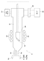
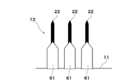
【解決手段】障壁層21と、障壁層21よりも小さい禁制帯幅からなり、単一の励起子のみを閉じ込めることが可能な量子ドット層22とを交互に2段以上に亘り積層させたロッド体12により構成され、障壁層21は、3〜10nmの厚みからなり、入射された光に基づいて各量子ドット層22に励起子が励起可能とされているとともに、その励起子が励起された各量子ドットに発生した電気双極子モーメントの方向を近接場光相互作用に基づいて互いに同一方向へ配向させ、この配列された双極子モーメントに基づいて最上段の量子ドット層22から放出するパルス光強度を増強させるとともに、パルス幅を狭小化させる。
【選択図】図2
Description
ロッド体12は、例えば図2(a)に示すように、障壁層21と、量子ドット層22とが交互に2段以上に亘り積層されている。図2(b)は、このロッド体12の拡大構成を示す図であるが、障壁層21は、禁制帯幅G1からなり、例えば、Zn1−xMgxO(xは、0.15〜0.3)で構成されている。また、この障壁層21は、3〜10nmの厚さで構成されていればよいが、以下の実施の形態においては、6nm程度で構成されている場合を例にとり説明をする。
11 基板
12 ロッド体
21 障壁層
22 量子ドット層
3 結晶成長装置
31 チャンバ
34 ステージ
36 ポンプ
37 圧力センサ
38 バタフライバルブ
51 RFヒータ
53 供給管
54 供給管
Claims (6)
- 障壁層と、上記障壁層よりも小さい禁制帯幅からなり、単一の励起子のみを閉じ込めることが可能な量子ドット層とを交互に2段以上に亘り積層させたロッドにより構成され、
上記障壁層は、3〜10nmの厚みからなり、
入射された光に基づいて上記各量子ドット層に励起子が励起可能とされているとともに、その励起子が励起された各量子ドットに発生した電気双極子モーメントの方向を近接場光相互作用に基づいて互いに同一方向へ配向させ、
この配列された双極子モーメントに基づいて多段の量子ドット層から放出するパルス光強度を増強させるとともに、パルス幅を狭小化させること
を特徴とする光パルス発生素子。 - 最上段の量子ドット層は、他の量子ドット層よりも膜厚が厚く構成されてなること
を特徴とする請求項1記載の光パルス発生素子。 - 上記障壁層は、5〜10nmの厚みからなり、さらに上記量子ドット層は、1〜10nmの厚みからなること
を特徴とする請求項1又は2記載の光パルス発生素子。 - 上記障壁層は、Zn1−xMgxO(xは、0.15〜0.3)であり、
上記量子ドット層は、ZnOであること
を特徴とする請求項1〜3のうち何れか1項記載の光パルス発生素子。 - 上記障壁層は、GaNであり、
上記量子ドット層は、InxGa1−xN(xは、0.1〜0.5)であること
を特徴とする請求項1〜3のうち何れか1項記載の光パルス発生素子。 - 上記障壁層は、GaN又はGaAsであり、
上記量子ドット層は、InAsであること
を特徴とする請求項1〜3のうち何れか1項記載の光パルス発生素子。
Priority Applications (1)
| Application Number | Priority Date | Filing Date | Title |
|---|---|---|---|
| JP2008191216A JP4753979B2 (ja) | 2008-07-24 | 2008-07-24 | 光パルス発生素子 |
Applications Claiming Priority (1)
| Application Number | Priority Date | Filing Date | Title |
|---|---|---|---|
| JP2008191216A JP4753979B2 (ja) | 2008-07-24 | 2008-07-24 | 光パルス発生素子 |
Publications (2)
| Publication Number | Publication Date |
|---|---|
| JP2010026463A true JP2010026463A (ja) | 2010-02-04 |
| JP4753979B2 JP4753979B2 (ja) | 2011-08-24 |
Family
ID=41732320
Family Applications (1)
| Application Number | Title | Priority Date | Filing Date |
|---|---|---|---|
| JP2008191216A Expired - Fee Related JP4753979B2 (ja) | 2008-07-24 | 2008-07-24 | 光パルス発生素子 |
Country Status (1)
| Country | Link |
|---|---|
| JP (1) | JP4753979B2 (ja) |
Cited By (1)
| Publication number | Priority date | Publication date | Assignee | Title |
|---|---|---|---|---|
| JPWO2013047003A1 (ja) * | 2011-09-26 | 2015-03-26 | パイオニア株式会社 | 近接場光デバイス、記録装置及びサンプル基板 |
Citations (4)
| Publication number | Priority date | Publication date | Assignee | Title |
|---|---|---|---|---|
| JPH08298340A (ja) * | 1995-04-27 | 1996-11-12 | Hitachi Ltd | 光パルス伝送システムおよび光パルス伝送素子 |
| JPH11231360A (ja) * | 1998-02-10 | 1999-08-27 | Hitachi Ltd | 光パルス圧縮装置およびそれを用いた光パルス伝送装置とレーザ光発生装置 |
| JP2000338453A (ja) * | 1999-05-26 | 2000-12-08 | Agency Of Ind Science & Technol | 半導体光パルス圧縮導波路素子 |
| JP2004518275A (ja) * | 2000-12-15 | 2004-06-17 | 科学技術振興事業団 | 量子ドットトリガー光子及びトリガー光子対の発生装置および方法 |
-
2008
- 2008-07-24 JP JP2008191216A patent/JP4753979B2/ja not_active Expired - Fee Related
Patent Citations (4)
| Publication number | Priority date | Publication date | Assignee | Title |
|---|---|---|---|---|
| JPH08298340A (ja) * | 1995-04-27 | 1996-11-12 | Hitachi Ltd | 光パルス伝送システムおよび光パルス伝送素子 |
| JPH11231360A (ja) * | 1998-02-10 | 1999-08-27 | Hitachi Ltd | 光パルス圧縮装置およびそれを用いた光パルス伝送装置とレーザ光発生装置 |
| JP2000338453A (ja) * | 1999-05-26 | 2000-12-08 | Agency Of Ind Science & Technol | 半導体光パルス圧縮導波路素子 |
| JP2004518275A (ja) * | 2000-12-15 | 2004-06-17 | 科学技術振興事業団 | 量子ドットトリガー光子及びトリガー光子対の発生装置および方法 |
Cited By (1)
| Publication number | Priority date | Publication date | Assignee | Title |
|---|---|---|---|---|
| JPWO2013047003A1 (ja) * | 2011-09-26 | 2015-03-26 | パイオニア株式会社 | 近接場光デバイス、記録装置及びサンプル基板 |
Also Published As
| Publication number | Publication date |
|---|---|
| JP4753979B2 (ja) | 2011-08-24 |
Similar Documents
| Publication | Publication Date | Title |
|---|---|---|
| Ng et al. | Group-III-nitride and halide-perovskite semiconductor gain media for amplified spontaneous emission and lasing applications | |
| Nanishi | The birth of the blue LED | |
| US20070220713A1 (en) | Method for Forming Zno Nano-Array and Zno Nanowall for Uv Laser On Silicon Substrate | |
| CN104201258B (zh) | 基于等离子体高调制带宽的可见光通信发光二极管的制备方法 | |
| CN102097564B (zh) | 量子点分子发光器件 | |
| GB2523423A (en) | Gas phase enhancement of emission color quality in solid state LEDs | |
| CN100375353C (zh) | 形成组合有半导体量子点的光电子器件有源区的方法 | |
| Li et al. | The developments of InP-based quantum dot lasers | |
| CN111200043B (zh) | 电泵浦量子点单光子源及其制备方法 | |
| JP4753979B2 (ja) | 光パルス発生素子 | |
| JP2000012961A (ja) | 半導体レーザ | |
| JP2011100779A (ja) | 半導体装置及びその製造方法 | |
| CN116865095A (zh) | 一种设有自束缚激子层的半导体激光元件 | |
| Mei et al. | Tunable InGaN quantum dot microcavity light emitters with 129 nm tuning range from yellow-green to violet | |
| Chen et al. | Picosecond tunable gain-switched blue pulses from GaN laser diodes with nanosecond current injections | |
| Li et al. | Controlling the aspect ratio of quantum dots: from columnar dots to quantum rods | |
| JP2009078942A (ja) | ZnOナノロッドの堆積方法 | |
| JP2009016710A (ja) | レーザ発振素子 | |
| JPH11121870A (ja) | 光半導体装置 | |
| Li et al. | Optimization of InAs/GaAs quantum-dot structures and application to 1.3-μm mode-locked laser diodes | |
| JP2000058978A (ja) | 半導体量子ドット素子とその製造方法 | |
| Tatebayashi et al. | Exploration of Nanowire Photonics towards Advent of Super-Smart Societies | |
| CN101593679A (zh) | 一种由砷化镓和锑化镓覆盖层调制的砷化铟量子点材料及其生长方法 | |
| Lim et al. | Observation of size-dependent resonance of near-field coupling between a deposited Zn dot and the probe apex during near-field optical chemical vapor deposition | |
| JP2005079182A (ja) | 半導体量子ドット素子及びその製造方法 |
Legal Events
| Date | Code | Title | Description |
|---|---|---|---|
| A01 | Written decision to grant a patent or to grant a registration (utility model) |
Free format text: JAPANESE INTERMEDIATE CODE: A01 Effective date: 20110510 |
|
| A01 | Written decision to grant a patent or to grant a registration (utility model) |
Free format text: JAPANESE INTERMEDIATE CODE: A01 |
|
| A61 | First payment of annual fees (during grant procedure) |
Free format text: JAPANESE INTERMEDIATE CODE: A61 Effective date: 20110524 |
|
| FPAY | Renewal fee payment (prs date is renewal date of database) |
Free format text: PAYMENT UNTIL: 20140603 Year of fee payment: 3 |
|
| R150 | Certificate of patent (=grant) or registration of utility model |
Free format text: JAPANESE INTERMEDIATE CODE: R150 |
|
| R250 | Receipt of annual fees |
Free format text: JAPANESE INTERMEDIATE CODE: R250 |
|
| S533 | Written request for registration of change of name |
Free format text: JAPANESE INTERMEDIATE CODE: R313533 |
|
| R350 | Written notification of registration of transfer |
Free format text: JAPANESE INTERMEDIATE CODE: R350 |
|
| LAPS | Cancellation because of no payment of annual fees |