JP2010017897A - Light emitting device and exposure system - Google Patents
Light emitting device and exposure system Download PDFInfo
- Publication number
- JP2010017897A JP2010017897A JP2008178631A JP2008178631A JP2010017897A JP 2010017897 A JP2010017897 A JP 2010017897A JP 2008178631 A JP2008178631 A JP 2008178631A JP 2008178631 A JP2008178631 A JP 2008178631A JP 2010017897 A JP2010017897 A JP 2010017897A
- Authority
- JP
- Japan
- Prior art keywords
- light emitting
- transfer
- light
- thyristors
- lighting signal
- Prior art date
- Legal status (The legal status is an assumption and is not a legal conclusion. Google has not performed a legal analysis and makes no representation as to the accuracy of the status listed.)
- Granted
Links
Images


Abstract
Description
本発明は、複数の発光素子を順次点灯させる発光装置、複数の発光素子を順次点灯させる発光チップを複数備えた露光装置に関する。 The present invention relates to a light emitting device for sequentially lighting a plurality of light emitting elements, and an exposure apparatus including a plurality of light emitting chips for sequentially lighting a plurality of light emitting elements.
電子写真方式を用いたプリンタや複写機等の画像形成装置において、感光体ドラム等の像保持体上を露光する露光装置として、近年、LED(Light Emitting Diode)等の発光素子をライン状に配列した発光素子アレイを用いたものが採用されている。 In an image forming apparatus such as a printer or a copying machine using an electrophotographic method, light emitting elements such as LEDs (Light Emitting Diodes) have recently been arranged in a line as an exposure apparatus that exposes an image carrier such as a photosensitive drum. The one using the light emitting element array is adopted.
公報記載の従来技術として、自己走査型発光素子アレイと呼ばれるものが存在する(特許文献1参照)。この自己走査型発光素子アレイでは、発光チップ内の各LEDを点灯させるためのスイッチ素子としてサイリスタ(転送サイリスタ)を用いている。なお、自己走査型発光素子アレイでは、LED自身もサイリスタ(発光サイリスタ)で構成される。そして、自己走査型発光素子アレイでは、入力される2本の転送信号によって各転送サイリスタを順次ターンオンさせ、ターンオンした転送サイリスタに対応する発光サイリスタを1個ずつ順次点灯可能な状態に設定する。一方、各発光サイリスタのアノード端子(あるいはカソード端子)に接続される一方の共通配線を一定電位に設定するとともに、各発光サイリスタのカソード端子(あるいはアノード端子)に接続される他方の共通配線には点灯信号を供給することで、点灯可能な状態に設定された発光サイリスタの点灯・消灯を指示する。そして、特許文献1には、発光チップ1枚あたり2系統の自己走査型発光素子アレイを形成し、各発光チップにそれぞれ2本ずつ点灯信号を供給することで、1発光チップ内において同時に点灯できる発光サイリスタの数を2個にすることが記載されている。
As a prior art described in the publication, there is a so-called self-scanning light emitting element array (see Patent Document 1). In this self-scanning light emitting element array, a thyristor (transfer thyristor) is used as a switch element for lighting each LED in the light emitting chip. In the self-scanning light-emitting element array, the LED itself is also composed of a thyristor (light-emitting thyristor). In the self-scanning light emitting element array, each transfer thyristor is sequentially turned on by two input transfer signals, and the light emitting thyristors corresponding to the turned-on transfer thyristors are set in a state where they can be sequentially turned on one by one. On the other hand, one common wiring connected to the anode terminal (or cathode terminal) of each light emitting thyristor is set to a constant potential, and the other common wiring connected to the cathode terminal (or anode terminal) of each light emitting thyristor is set to By supplying a lighting signal, the light-emitting thyristor that is set in a lighting-enabled state is instructed to be turned on / off. In
また、別の公報記載の従来技術として、自己走査型発光素子アレイにおいて各転送サイリスタにそれぞれ2個の発光サイリスタを接続するとともに、奇数番目に配列される発光サイリスタに対しては第1の書き込み信号を供給し、偶数番目に配列される発光サイリスタに対しては第2の書き込み信号を供給することで、1発光チップ内において同時に点灯できる発光サイリスタの数を2個にするものも存在する(特許文献2参照)。 As another prior art described in another publication, in the self-scanning light emitting element array, two light emitting thyristors are connected to each transfer thyristor, and the first write signal is applied to the light emitting thyristors arranged in an odd number. And the second write signal is supplied to even-numbered light-emitting thyristors, so that there are two light-emitting thyristors that can be turned on simultaneously in one light-emitting chip (patent) Reference 2).
ところで、近年の画像形成装置の高画質化に伴い、主走査方向の出力解像度(主走査方向解像度と呼ぶ)は、より高くなる傾向にある。このため、従来機では例えば600dpiであった主走査方向解像度が、1200dpiさらには2400dpiになってきている。なお、発光素子アレイを用いた露光装置では、主走査方向解像度に応じて発光素子の数および配置間隔を設定する必要がある。例えば主走査方向解像度が1200dpi(dot per inch)の場合は、主走査方向解像度が600dpiの場合に対して発光素子の数を2倍にし、且つ、発光素子の配置間隔を2分の1にする必要がある。 By the way, with the recent increase in image quality of image forming apparatuses, output resolution in the main scanning direction (referred to as main scanning direction resolution) tends to be higher. For this reason, the resolution in the main scanning direction, which was 600 dpi for example in the conventional machine, has become 1200 dpi or even 2400 dpi. In the exposure apparatus using the light emitting element array, it is necessary to set the number of light emitting elements and the arrangement interval according to the resolution in the main scanning direction. For example, when the resolution in the main scanning direction is 1200 dpi (dot per inch), the number of light emitting elements is doubled and the arrangement interval of the light emitting elements is halved as compared with the case where the resolution in the main scanning direction is 600 dpi. There is a need.
ここで、1つの露光装置を、第1の主走査方向解像度(例えば1200dpi)で画像形成を行う画像形成装置と、第1の主走査方向解像度の半分となる第2の主走査方向解像度(例えば600dpi)で画像形成を行う画像形成装置とで共用することが考えられる。 Here, one exposure apparatus uses an image forming apparatus that forms an image with a first main scanning direction resolution (for example, 1200 dpi), and a second main scanning direction resolution (for example, half the first main scanning direction resolution). It may be shared with an image forming apparatus that forms an image at 600 dpi).
しかしながら、例えば1つの自己走査型発光素子アレイを有する発光チップを用いた場合には、点灯信号が発光サイリスタ1個おきに供給されるよう、点灯信号の供給条件を変更する必要があり、自己走査型発光素子アレイを駆動する駆動回路が大規模なものとなってしまう。
また、例えば2つの自己走査型発光素子アレイを有する発光チップを用い、この発光チップに一方の点灯信号のみを供給した場合には、点灯信号が供給される側の自己走査型発光素子アレイによって主走査方向の長さが半分となった画像が形成され、点灯信号が供給されない側の自己走査型発光素子アレイによって画像が形成されなくなるという事態を招いてしまう。
However, for example, when a light-emitting chip having one self-scanning light-emitting element array is used, it is necessary to change the lighting signal supply condition so that the lighting signal is supplied every other light-emitting thyristor. The drive circuit for driving the type light emitting element array becomes large-scale.
For example, when a light emitting chip having two self-scanning light emitting element arrays is used and only one lighting signal is supplied to the light emitting chip, the self-scanning light emitting element array on the side to which the lighting signal is supplied is used. An image in which the length in the scanning direction is halved is formed, resulting in a situation in which no image is formed by the self-scanning light emitting element array on the side where the lighting signal is not supplied.
これに対し、例えば1つの自己走査型発光素子アレイを有する発光チップにおいて、1つの転送サイリスタに2つの発光サイリスタを接続する構成を採用し、一方の点灯信号のみを供給した場合には、発光サイリスタが1個おきに点灯可能となり、元の画像データに対応する画像が得られることになる。ただし、この場合には、点灯可能となる発光サイリスタの位置が発光素子アレイに沿って一方向に移動するため、複数の発光チップが並べられた露光装置を用いて主走査方向に沿う直線状の細線画像を形成した場合に、発光素子アレイの主走査方向長さを周期とするジグザグ状の文様が目立つようになり、画質が低下してしまうおそれがあった。 On the other hand, for example, in a light-emitting chip having one self-scanning light-emitting element array, when a configuration in which two light-emitting thyristors are connected to one transfer thyristor and only one lighting signal is supplied, the light-emitting thyristor Can be turned on every other, and an image corresponding to the original image data can be obtained. However, in this case, since the position of the light-emitting thyristor that can be turned on moves in one direction along the light-emitting element array, a linear shape along the main scanning direction is used by using an exposure apparatus in which a plurality of light-emitting chips are arranged. When a thin line image is formed, a zigzag pattern with the length in the main scanning direction of the light emitting element array as a period becomes conspicuous, and there is a possibility that the image quality is deteriorated.
本発明は、第1の主走査方向解像度で動作が可能であるとともに、第1の主走査方向解像度の半分の第2の主走査方向解像度で動作する際にジグザグ状の文様の発生を抑制することを目的とする。 The present invention can operate at the first main scanning direction resolution, and suppresses the generation of zigzag patterns when operating at the second main scanning direction resolution which is half the first main scanning direction resolution. For the purpose.
請求項1記載の発明は、一列に並べて配置され、点灯信号により点灯/非点灯が制御される複数の発光素子を有する発光素子列と、前記複数の発光素子にそれぞれ対応して設けられ、オン状態に設定されることにより対応する発光素子を点灯可能状態とする複数のスイッチ素子を有するスイッチ素子列とを備え、前記発光素子列が、前記発光素子列において奇数番目に配列される発光素子で構成され、前記点灯信号として共通の第1点灯信号が供給される第1発光素子群と、前記発光素子列において偶数番目に配列される発光素子で構成され、当該点灯信号として共通の第2点灯信号が供給される第2発光素子群とを有し、前記スイッチ素子列が、前記第1発光素子群に属する発光素子および前記第2発光素子群に属する発光素子のうち、前記発光素子列の一端側に配列される発光素子で構成される一端側発光素子群の各発光素子を、第1の方向に沿って順次発光可能な状態に設定する第1スイッチ素子群と、前記第1発光素子群に属する発光素子および前記第2発光素子群に属する発光素子のうち、前記発光素子列の他端側に配列される発光素子で構成される他端側発光素子群の各発光素子を、前記第1の方向とは逆の第2の方向に沿って順次発光可能な状態に設定する第2スイッチ素子群とを有することを特徴とする発光装置である。 According to the first aspect of the present invention, a light emitting element array having a plurality of light emitting elements which are arranged in a line and whose lighting / non-lighting is controlled by a lighting signal is provided corresponding to each of the plurality of light emitting elements. A switch element array having a plurality of switch elements that can turn on the corresponding light-emitting elements by being set to a state, and the light-emitting element array is a light-emitting element arranged in an odd number in the light-emitting element array A first light emitting element group configured to be supplied with a common first lighting signal as the lighting signal, and light emitting elements arranged in an even number in the light emitting element row, and a common second lighting as the lighting signal. A second light emitting element group to which a signal is supplied, and the switch element row includes a light emitting element belonging to the first light emitting element group and a light emitting element belonging to the second light emitting element group. A first switch element group for setting each light emitting element of the one end side light emitting element group configured by the light emitting elements arranged on one end side of the light emitting element row in a state capable of sequentially emitting light along a first direction; Of the light emitting elements belonging to the first light emitting element group and the light emitting elements belonging to the second light emitting element group, each light emission of the other end side light emitting element group constituted by the light emitting elements arranged on the other end side of the light emitting element row. A light emitting device comprising: a second switch element group that sets elements in a state capable of sequentially emitting light along a second direction opposite to the first direction.
請求項2記載の発明は、前記第1点灯信号を前記第1発光素子群に供給し、前記第2点灯信号を前記第2発光素子群に供給する点灯信号発生部と、前記点灯信号発生部が前記第1点灯信号および前記第2点灯信号の両方を供給する第1のモードと、当該点灯信号発生部が当該第1点灯信号または当該第2点灯信号のいずれか一方のみを供給する第2のモードとを切り換える切り換え部とをさらに含むことを特徴とする請求項1記載の発光装置である。
請求項3記載の発明は、前記第1発光素子群を構成する発光素子の数と前記第2発光素子群を構成する発光素子の数とが偶数且つ同数であることを特徴とする請求項1または2記載の発光装置である。
請求項4記載の発明は、前記複数の発光素子および前記複数のスイッチ素子がサイリスタで構成されることを特徴とする請求項1乃至3のいずれか1項記載の発光装置である。
According to a second aspect of the present invention, there is provided a lighting signal generator that supplies the first lighting signal to the first light emitting element group and supplies the second lighting signal to the second light emitting element group, and the lighting signal generator. A first mode in which both the first lighting signal and the second lighting signal are supplied, and a second mode in which the lighting signal generator supplies only either the first lighting signal or the second lighting signal. The light emitting device according to
The invention described in
A fourth aspect of the present invention is the light emitting device according to any one of the first to third aspects, wherein the plurality of light emitting elements and the plurality of switch elements are formed of thyristors.
請求項5記載の発明は、複数の第1転送サイリスタを一列に並べて配列し、隣接する第1転送サイリスタのゲート間をそれぞれダイオードにて一方向に電流が流れるように接続し、各々の第1転送サイリスタのアノードまたはカソードを、第1転送信号が入力される第1転送信号端子と第2転送信号が入力される第2転送信号端子とに対して配列方向に交互に接続してなる第1転送ブロックと、前記第1転送ブロックに隣接して複数の第2転送サイリスタを一列に並べて配列し、隣接する第2転送サイリスタのゲート間をそれぞれダイオードにて前記一方向とは逆方向に電流が流れるように接続し、各々の第2転送サイリスタのアノードまたはカソードを、前記第1転送信号端子と前記第2転送信号端子とに対して配列方向に交互に接続してなる第2転送ブロックと、複数の第1発光サイリスタを一列に配列してなり、各々の第1発光サイリスタのゲートと前記第1転送ブロックにおける奇数番目の第1転送サイリスタのゲートおよび前記第2転送ブロックの奇数番目の第2転送サイリスタのゲートとをそれぞれ接続し、各々の第1発光サイリスタのアノードまたはカソードには共通の第1点灯信号が供給される第1発光ブロックと、隣接する前記第1発光サイリスタ間に複数の第2発光サイリスタをそれぞれ配置してなり、各々の第2発光サイリスタのゲートと前記第1転送ブロックの偶数番目の第1転送サイリスタのゲートおよび前記第2転送ブロックの偶数番目の第2転送サイリスタのゲートとをそれぞれ接続し、各々の第2発光サイリスタのアノードまたはカソードには共通の第2点灯信号が供給される第2発光ブロックとを含む発光装置である。 According to a fifth aspect of the present invention, a plurality of first transfer thyristors are arranged in a line, and the gates of adjacent first transfer thyristors are connected to each other so that current flows in one direction by a diode. A first thyristor in which an anode or a cathode of a transfer thyristor is alternately connected in the arrangement direction to a first transfer signal terminal to which a first transfer signal is input and a second transfer signal terminal to which a second transfer signal is input. A transfer block and a plurality of second transfer thyristors are arranged in a line adjacent to the first transfer block, and a current flows in the direction opposite to the one direction by a diode between the gates of the adjacent second transfer thyristors. The second transfer thyristors are connected so that the anodes or cathodes of the second transfer thyristors are alternately connected to the first transfer signal terminal and the second transfer signal terminal in the arrangement direction. A second transfer block and a plurality of first light-emitting thyristors arranged in a line, the gate of each first light-emitting thyristor, the gate of the odd-numbered first transfer thyristor and the second transfer in the first transfer block. The gates of the odd-numbered second transfer thyristors of the block are connected to each other, and the first light-emitting block adjacent to the first light-emitting block in which a common first lighting signal is supplied to the anode or the cathode of each first light-emitting thyristor. A plurality of second light-emitting thyristors are respectively arranged between the light-emitting thyristors, and each second light-emitting thyristor gate, the even-numbered first transfer thyristor gate of the first transfer block, and the even-numbered second transfer block. Are connected to the gates of the second transfer thyristors, and the anode or cathode of each second light-emitting thyristor is shared. The second lighting signal is a light emitting device including a can and a second light-emitting blocks to be supplied.
請求項6記載の発明は、複数の第1転送サイリスタを一列に並べて配列し、隣接する第1転送サイリスタのゲート間をそれぞれダイオードにて一方向に電流が流れるように接続し、各々の第1転送サイリスタのアノードまたはカソードを、第1転送信号が入力される第1転送信号端子と第2転送信号が入力される第2転送信号端子とに対して配列方向に交互に接続してなる第1転送ブロックと、前記第1転送ブロックに隣接して複数の第2転送サイリスタを一列に並べて配列し、隣接する第2転送サイリスタのゲート間をそれぞれダイオードにて前記一方向とは逆方向に電流が流れるように接続し、各々の第2転送サイリスタのアノードまたはカソードを、前記第1転送信号端子と前記第2転送信号端子とに交互に接続してなる第2転送ブロックと、複数の第1発光サイリスタを一列に配列してなり、各々の第1発光サイリスタのアノードまたはカソードには共通の第1点灯信号が供給される第1発光ブロックと、複数の第2発光サイリスタを前記複数の第1発光サイリスタと交互に配列してなり、各々の第1発光サイリスタのアノードまたはカソードには共通の第2点灯信号が供給される第2発光ブロックとを備え、前記第1発光ブロックを構成する前記複数の第1発光サイリスタのうち、一部の第1発光サイリスタのゲートを、前記第1転送ブロックを構成する前記第1転送サイリスタのゲートにそれぞれ接続するとともに、残りの第1発光サイリスタのゲートを、前記第2転送ブロックを構成する前記第2転送サイリスタのゲートにそれぞれ接続し、前記第2発光ブロックを構成する前記複数の第2発光サイリスタのうち、一部の第2発光サイリスタのゲートを、前記第1転送ブロックを構成し且つ前記第1発光サイリスタが接続されていない前記第1転送サイリスタのゲートにそれぞれ接続するとともに、残りの第2発光サイリスタのゲートを、前記第2転送ブロックを構成し且つ当該第1発光サイリスタが接続されていない前記第2転送サイリスタにそれぞれ接続することを特徴とする発光装置である。 According to a sixth aspect of the present invention, a plurality of first transfer thyristors are arranged in a line, and the gates of adjacent first transfer thyristors are connected so that current flows in one direction by a diode, respectively. A first thyristor in which an anode or a cathode of a transfer thyristor is alternately connected in the arrangement direction to a first transfer signal terminal to which a first transfer signal is input and a second transfer signal terminal to which a second transfer signal is input. A transfer block and a plurality of second transfer thyristors are arranged in a line adjacent to the first transfer block, and a current flows in the direction opposite to the one direction by a diode between the gates of the adjacent second transfer thyristors. A second transfer block in which the second transfer thyristor is connected to the first transfer signal terminal and the second transfer signal terminal alternately. And a plurality of first light-emitting thyristors arranged in a line, and a first light-emitting block in which a common first lighting signal is supplied to the anode or cathode of each first light-emitting thyristor, and a plurality of second light-emitting elements The first light emitting thyristor is alternately arranged with the plurality of first light emitting thyristors, and each of the first light emitting thyristors includes a second light emitting block to which a common second lighting signal is supplied. Among the plurality of first light-emitting thyristors constituting the light-emitting block, the gates of some of the first light-emitting thyristors are connected to the gates of the first transfer thyristors constituting the first transfer block, respectively, and the remaining first A gate of one light emitting thyristor is connected to each gate of the second transfer thyristor constituting the second transfer block, and the second light emitting block is connected to the second light emitting thyristor. Among the plurality of second light-emitting thyristors that are formed, the gates of some of the second light-emitting thyristors constitute gates of the first transfer thyristors that constitute the first transfer block and that are not connected to the first light-emitting thyristor. A light-emitting device that is connected to each other and that connects the gates of the remaining second light-emitting thyristors to the second transfer thyristor that constitutes the second transfer block and that is not connected to the first light-emitting thyristor. It is.
請求項7記載の発明は、前記第1転送ブロックにおいて、各々の前記第1転送サイリスタのゲートは、抵抗を介して共通の配線に接続され、前記第2転送ブロックにおいて、各々の前記第2転送サイリスタのゲートは、抵抗を介して前記共通の配線に接続されることを特徴とする請求項5または6記載の発光装置である。
請求項8記載の発明は、前記第1点灯信号を前記第1発光ブロックに供給し、前記第2点灯信号を前記第2発光ブロックに供給する点灯信号発生部と、前記点灯信号発生部が前記第1点灯信号および前記第2点灯信号の両方を供給する第1のモードと、当該点灯信号発生部が当該第1点灯信号または当該第2点灯信号のいずれか一方のみを供給する第2のモードとを切り換える切り換え部とをさらに含むことを特徴とする請求項5乃至7のいずれか1項記載の発光装置である。
請求項9記載の発明は、前記第1発光ブロックを構成する発光サイリスタの数と前記第2発光ブロックを構成する発光サイリスタの数とが偶数且つ同数であることを特徴とする請求項5乃至8のいずれかに1項記載の発光装置である。
According to a seventh aspect of the present invention, in the first transfer block, a gate of each of the first transfer thyristors is connected to a common wiring through a resistor, and each second transfer in the second transfer block 7. The light emitting device according to
According to an eighth aspect of the present invention, a lighting signal generator that supplies the first lighting signal to the first light-emitting block and supplies the second lighting signal to the second light-emitting block, and the lighting signal generator is the A first mode that supplies both the first lighting signal and the second lighting signal, and a second mode in which the lighting signal generator supplies only one of the first lighting signal or the second lighting signal. The light-emitting device according to
The invention according to claim 9 is characterized in that the number of light-emitting thyristors constituting the first light-emitting block and the number of light-emitting thyristors constituting the second light-emitting block are an even number and the same number. The light-emitting device according to any one of the above.
請求項10記載の発明は、複数の発光素子が主走査方向に並べて配列された発光素子列を有する発光チップを、主走査方向に複数配列してなる発光部を備え、帯電された像保持体を露光する露光装置であって、前記発光チップは、前記複数の発光素子にそれぞれ対応して設けられ、オン状態に設定されることにより対応する発光素子を点灯可能状態とする複数のスイッチ素子を有するスイッチ素子列を備え、前記発光素子列が、前記発光素子列において奇数番目に配列される発光素子で構成され、点灯信号として共通の第1点灯信号が供給される第1発光素子群と、前記発光素子列において偶数番目に配列される発光素子で構成され、前記点灯信号として共通の第2点灯信号が供給される第2発光素子群とを有し、前記スイッチ素子列が、前記第1発光素子群に属する発光素子および前記第2発光素子群に属する発光素子のうち、前記発光素子列の一端側に配列される発光素子で構成される一端側発光素子群の各発光素子を、第1の方向に沿って順次発光可能な状態に設定する第1スイッチ素子群と、
前記第1発光素子群に属する発光素子および前記第2発光素子群に属する発光素子のうち、前記発光素子列の他端側に配列される発光素子で構成される他端側発光素子群の各発光素子を、前記第1の方向とは逆の第2の方向に沿って順次発光可能な状態に設定する第2スイッチ素子群とを有することを特徴とする露光装置である。
According to a tenth aspect of the present invention, there is provided a charged image carrier including a light emitting section in which a plurality of light emitting chips each having a light emitting element array in which a plurality of light emitting elements are arranged in the main scanning direction are arranged in the main scanning direction. The light-emitting chip is provided corresponding to each of the plurality of light-emitting elements, and a plurality of switch elements that turn on the corresponding light-emitting elements by being set to an on state are provided. A first light emitting element group that is configured by light emitting elements arranged in an odd number in the light emitting element array and to which a common first lighting signal is supplied as a lighting signal; A second light emitting element group which is configured by even-numbered light emitting elements in the light emitting element array and to which a common second lighting signal is supplied as the lighting signal. Among the light emitting elements belonging to the first light emitting element group and the light emitting elements belonging to the second light emitting element group, each light emitting element of the one end side light emitting element group constituted by the light emitting elements arranged on one end side of the light emitting element row is A first switch element group that is set in a state capable of sequentially emitting light along the first direction;
Of the light emitting elements belonging to the first light emitting element group and the light emitting elements belonging to the second light emitting element group, each of the other end side light emitting element groups configured by light emitting elements arranged on the other end side of the light emitting element row. An exposure apparatus comprising: a second switch element group configured to sequentially set light emitting elements in a state capable of emitting light along a second direction opposite to the first direction.
請求項11記載の発明は、前記発光部において主走査方向に奇数番目に配列される発光チップと偶数番目に配列される発光チップとが、副走査方向にずらされることにより千鳥状に配列されるとともに、当該奇数番目に配列される発光チップと当該偶数番目に配列される発光チップとが副走査方向に逆向きに取り付けられ、前記第1点灯信号を前記第1発光素子群に供給し、前記第2点灯信号を前記第2発光素子群に供給する点灯信号発生部と、前記点灯信号発生部が前記第1点灯信号および前記第2点灯信号の両方を供給する第1のモードと、当該点灯信号発生部が当該第1点灯信号または当該第2点灯信号のいずれか一方のみを供給する第2のモードとを切り換える切り換え部とを備え、前記切り換え部は、前記第2のモードにおいて、前記奇数番目に配列される発光チップに対して前記第1点灯信号または前記第2点灯信号を供給し、前記偶数番目に配列される発光チップに対しては当該奇数番目に配列される発光チップに供給しない方の当該第2点灯信号または当該第1点灯信号を供給することを特徴とする請求項10記載の露光装置である。
請求項12記載の発明は、前記発光チップにおいて前記第1発光素子群を構成する発光素子の数と前記第2発光素子群を構成する発光素子の数とが偶数且つ同数であることを特徴とする請求項10または11記載の露光装置である。
請求項13記載の発明は、前記発光チップを構成する前記複数の発光素子および前記複数のスイッチ素子がサイリスタで構成されることを特徴とする請求項10乃至12のいずれか1項記載の露光装置である。
In the invention described in
The invention according to
According to a thirteenth aspect of the present invention, in the exposure apparatus according to any one of the tenth to twelfth aspects, the plurality of light emitting elements and the plurality of switch elements constituting the light emitting chip are formed of thyristors. It is.
請求項1記載の発明によれば、第1の主走査方向解像度での発光が可能であるとともに、第1の主走査方向解像度の半分の第2の主走査方向解像度で発光する際にジグザグ状の文様の発生を抑制することができる。
請求項2記載の発明によれば、本構成を有しない場合と比較して、第1の主走査方向解像度と第2の主走査方向解像度との切り換えを容易に行うことができる。
請求項3記載の発明によれば、同一の発光素子群内において発光可能な発光素子を1つだけとすることができる。
請求項4記載の発明によれば、本構成を有しない場合と比較して、点灯可能な状態となる発光素子の切り換えを高速化することができる。
請求項5記載の発明によれば、第1の主走査方向解像度での発光が可能であるとともに、第1の主走査方向解像度の半分の第2の主走査方向解像度で発光する際にジグザグ状の文様の発生を抑制することができる。
請求項6記載の発明によれば、第1の主走査方向解像度での発光が可能であるとともに、第1の主走査方向解像度の半分の第2の主走査方向解像度で発光する際にジグザグ状の文様の発生を抑制することができる。
請求項7記載の発明によれば、転送サイリスタからこのサイリスタに隣接する他の転送サイリスタへの転送動作を安定させることができる。
請求項8記載の発明によれば、本構成を有しない場合と比較して、第1の主走査方向解像度と第2の主走査方向解像度との切り換えを容易に行うことができる。
請求項9記載の発明によれば、同一の発光ブロック内において発光可能な発光素子を1つだけとすることができる。
請求項10記載の発明によれば、像保持体に対し第1の主走査方向解像度での露光が可能であるとともに、第1の主走査方向解像度の半分の第2の主走査方向解像度で露光を行う際にジグザグ状の文様の発生を抑制することができる。
請求項11記載の発明によれば、第1の主走査方向解像度で露光を行った場合に、点灯可能となる発光サイリスタの間隔を発光チップ内および隣接する発光チップ間で一定にすることができ、また、第2の主走査方向解像度で露光を行った場合に、点灯可能となる発光サイリスタの間隔を発光チップ内および発光チップ間で一定にすることができる。
請求項12記載の発明によれば、1つの発光チップの同一の発光素子群内において発光可能な発光素子を1つだけとすることができる。
請求項13記載の発明によれば、本構成を有しない場合と比較して、点灯可能な状態となる発光素子の切り換えを高速化することができる。
According to the first aspect of the present invention, light can be emitted with the first main scanning direction resolution, and zigzag when emitting light with the second main scanning direction resolution which is half of the first main scanning direction resolution. The occurrence of patterns can be suppressed.
According to the second aspect of the present invention, it is possible to easily switch between the first main scanning direction resolution and the second main scanning direction resolution as compared with the case where this configuration is not provided.
According to the third aspect of the present invention, only one light emitting element capable of emitting light in the same light emitting element group can be provided.
According to the fourth aspect of the present invention, it is possible to speed up the switching of the light emitting elements that can be turned on as compared with the case where the present configuration is not provided.
According to the fifth aspect of the present invention, light can be emitted with the first main scanning direction resolution, and zigzag when emitting light with the second main scanning direction resolution which is half of the first main scanning direction resolution. The occurrence of patterns can be suppressed.
According to the sixth aspect of the present invention, the light can be emitted with the first main scanning direction resolution, and zigzag when the light is emitted with the second main scanning direction resolution which is half of the first main scanning direction resolution. The occurrence of patterns can be suppressed.
According to the seventh aspect of the invention, the transfer operation from the transfer thyristor to another transfer thyristor adjacent to the thyristor can be stabilized.
According to the eighth aspect of the present invention, it is possible to easily switch between the first main scanning direction resolution and the second main scanning direction resolution as compared with the case where this configuration is not provided.
According to the ninth aspect of the present invention, only one light emitting element capable of emitting light in the same light emitting block can be provided.
According to the tenth aspect of the present invention, the image carrier can be exposed at the first main scanning direction resolution and exposed at the second main scanning direction resolution which is half of the first main scanning direction resolution. The generation of zigzag patterns can be suppressed when performing.
According to the invention described in
According to the twelfth aspect of the present invention, only one light emitting element that can emit light within the same light emitting element group of one light emitting chip can be provided.
According to the thirteenth aspect of the present invention, it is possible to speed up the switching of the light emitting elements that can be turned on as compared with the case where this configuration is not provided.
以下、添付図面を参照して、本発明の実施の形態について詳細に説明する。
<実施の形態1>
図1は、本実施の形態が適用される画像形成装置1の全体構成の一例を示した図である。同図に示す画像形成装置1は、各色の画像データに対応して画像形成を行う画像形成プロセス部10、画像形成装置1全体の動作を制御する制御部30、パーソナルコンピュータや画像読取装置等といった外部装置(図示せず)に接続され、これらから受信した画像データに対して画像処理を施す画像処理部35を備えている。
Embodiments of the present invention will be described below in detail with reference to the accompanying drawings.
<
FIG. 1 is a diagram illustrating an example of the overall configuration of an
画像形成プロセス部10は、一定の間隔を置いて配置される4つの画像形成ユニット11(具体的には11Y、11M、11C、11K)を備える。各画像形成ユニット11は、感光層(図示せず)が形成された像保持体の一例としての感光体ドラム12、感光体ドラム12を帯電する帯電器13、帯電器13で帯電された感光体ドラム12を画像データに基づいて露光する露光装置の一例としてのLEDプリントヘッド(LPH)14、感光体ドラム12上に形成された静電潜像を現像する現像器15、感光体ドラム12表面を清掃するクリーナ16を備えている。ここで、各画像形成ユニット11は、現像器15に収納されるトナーを除いて、略同様に構成されている。そして、各画像形成ユニット11は、それぞれがイエロー(Y)、マゼンタ(M)、シアン(C)、黒(K)のトナー像を形成する。
The image forming
さらに、画像形成プロセス部10は、各画像形成ユニット11の感光体ドラム12に対向する位置を循環する中間転写ベルト20、中間転写ベルト20を挟んで各感光体ドラム12に対向配置される一次転写ロール21、中間転写ベルト20に対向配置される二次転写ロール22、二次転写後の用紙の未定着画像を加熱・加圧して定着する定着器45を備えている。
Further, the image forming
この画像形成装置1において、画像形成プロセス部10は、制御部30から供給される各種の制御信号に基づいて画像形成動作を行う。そして、制御部30による制御の下で、外部装置から入力された画像データは、画像処理部35によって画像処理が施され、各画像形成ユニット11に供給される。そして、例えば黒(K)色の画像形成ユニット11Kでは、感光体ドラム12が矢印A方向に回転しながら、帯電器13により予め定められた電位に帯電され、画像処理部35から送信された画像データに基づいて発光するLPH14により露光される。これにより、感光体ドラム12上には、黒(K)色画像に関する静電潜像が形成される。そして、感光体ドラム12上に形成された静電潜像は現像器15により現像され、感光体ドラム12上には黒(K)色のトナー像が形成される。同様に、画像形成ユニット11Y、11M、11Cにおいても、それぞれイエロー(Y)、マゼンタ(M)、シアン(C)の各色トナー像が形成される。
In the
各画像形成ユニット11で形成された各色トナー像は、矢印B方向に移動する中間転写ベルト20上に、一次転写ロール21により順次静電吸引されて、各色トナーが重畳された合成トナー像となる。中間転写ベルト20上の合成トナー像は、中間転写ベルト20の移動に伴って二次転写ロール22が配置された領域(二次転写部T)に搬送される。合成トナー像が二次転写部Tに搬送されるタイミングに合わせて、用紙が用紙保持部40から二次転写部Tに供給される。そして、二次転写部Tにて二次転写ロール22により形成される転写電界により、合成トナー像は搬送されてきた用紙上に一括して静電転写される。
The respective color toner images formed by the respective
その後、合成トナー像が静電転写された用紙は、中間転写ベルト20から剥離され、定着器45まで搬送される。定着器45に搬送された用紙上の合成トナー像は、定着器45によって熱および圧力による定着処理を受けて用紙上に定着される。そして、定着画像が形成された用紙は、画像形成装置1の排出部に設けられた排紙積載部41に搬送される。一方、二次転写後の中間転写ベルト20に残存するトナーは、二次転写の終了後に中間転写ベルト20表面からベルトクリーナ25によって除去される。
Thereafter, the sheet on which the synthetic toner image has been electrostatically transferred is peeled off from the
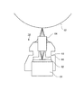
図2は、LPH14の構成を示した断面図である。このLPH14は、ハウジング61、複数のLED(本実施の形態では発光サイリスタ)を備えた発光部63、発光部63や発光部63を駆動する信号発生回路100(後段の図5参照)等を搭載する回路基板62、発光部63から出射された光を感光体ドラム12表面に結像させるロッドレンズアレイ64、ロッドレンズアレイ64を支持するとともに発光部63を外部から遮蔽するホルダ65を備えている。
FIG. 2 is a cross-sectional view showing the configuration of the
ハウジング61は、例えば金属で形成され、回路基板62を支持している。ロッドレンズアレイ64は、感光体ドラム12の軸方向に沿って配置されるとともに、感光体ドラム12の回転方向に幅をもって形成されている。ホルダ65は、感光体ドラム12の軸方向に沿って配置されて、発光部63を密閉する。また、ホルダ65は、ハウジング61およびロッドレンズアレイ64を支持し、発光部63の発光点とロッドレンズアレイ64の焦点面とが一致するように設定されている。
The
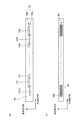
図3(a)はLPH14における回路基板62および発光部63の上面図であり、図3(b)はLPH14におけるロッドレンズアレイ64およびホルダ65の上面図である。図3(a)に示すように、発光部63は、回路基板62上に、発光装置の一例としての60個の発光チップC(C1〜C60)を、副走査方向に二列に千鳥状に配置して構成されている。なお、発光部63のうち、副走査方向上流側において主走査方向に一列に配置される奇数番目の発光チップC1、C3、…、C59を第1チップ列63aと呼び、副走査方向下流側において主走査方向に一列に配置される偶数番目の発光チップC2、…、C58、C60を第2チップ列63bと呼ぶ。
FIG. 3A is a top view of the
そして、各発光チップC1〜C60には、後述するようにそれぞれ256個の発光サイリスタが搭載されており、発光部63全体では15360個の発光サイリスタが設けられている。また、発光チップC1(後述する発光素子アレイ71)の外側端部から発光チップC60(後述する発光素子アレイ71)の外側端部までの距離(発光部63の主走査方向長さ)は、A3ノビの用紙Pへの画像形成に対応するために324mmに設定される。このため、隣接する発光サイリスタはそれぞれ約21.15μmの等間隔に配置され、このLPH14の主走査方向解像度は1200dpi(dot per inch)となっている。
Each of the light emitting chips C1 to C60 is provided with 256 light emitting thyristors as described later, and the
また、図3(b)に示すように、ロッドレンズアレイ64は、複数のロッドレンズ64aを、互い違いとなるように副走査方向に二列に整列配置した状態で、ホルダ65に保持させることによって構成されている。各ロッドレンズ64aは例えば円柱状の形状を有しており、その半径方向に屈折率分布を有し正立等倍実像を形成する屈折率分布型レンズにて構成される。このような屈折率分布型レンズとしては、例えばセルフォック(日本板硝子株式会社の商標)レンズアレイが挙げられる。
Further, as shown in FIG. 3B, the
図4は、上記発光部63のうち、発光チップC1、C2、C3の連結部位を拡大した図である。ここで、発光チップC1〜C60はすべて同一の構成を有しており、例えば発光チップC2を例とすると、矩形状のチップ基板70と、このチップ基板70の表面に長手方向に沿って一列に配置された発光素子アレイ71とを備えている。この発光素子アレイ71は、主走査方向に一列に並べられた256個の発光サイリスタを有している。また、発光素子アレイ71は、チップ基板70の表面の短手方向の一方の側に偏倚した位置に取り付けられている。そして、第1チップ列63aを構成する発光チップC1、C3(…、C59)と、第2チップ列63bを構成する発光チップC2(…、C58、C60)とが、副走査方向に逆を向くように配置されており、その結果、副走査方向において第1チップ列63aを構成する発光素子アレイ71と第2チップ列63bを構成する発光素子アレイ71とが副走査方向に近接するようになっている。そして、図4に示したように、発光チップC1、C2、C3のそれぞれに配置された発光素子アレイ71の端部境界において、発光素子アレイ71が発光チップC1、C2の連結部および発光チップC2、C3の連結部で主走査方向に連続するように配列されている。
FIG. 4 is an enlarged view of a connection portion of the light emitting chips C1, C2, and C3 in the
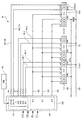
図5は、回路基板62(図2参照)に搭載される信号発生回路100の構成および回路基板62の配線構成を示した図である。
信号発生回路100には、画像処理部35(図1参照)より、ライン同期信号Lsync、ビデオデータVdata、クロック信号clk、およびリセット信号RST等の各種制御信号が入力されるようになっている。そして、信号発生回路100は、外部から入力されてくる各種制御信号に基づいて、例えばビデオデータVdataの並べ替えや出力値の補正等を行い、各発光チップC(C1〜C60)に対して点灯信号φI(φI1〜φI120)を出力する点灯信号発生部110を備えている。また、各発光チップCでは、搭載される256個の発光サイリスタを128個ずつ2組に分け、各組(128個の発光サイリスタ)を1スレッドとして点灯制御を行っている。このため、各発光チップC1〜C60には、2本の点灯信号φI(例えば発光チップC1ではφI1およびφI2)が供給される。なお、回路基板62には、信号発生回路100における点灯信号発生部110の動作切り換えを設定するため切り換え部の一例としての切換スイッチ130が設けられている。
FIG. 5 is a diagram showing the configuration of the
The
また、信号発生回路100は、外部から入力されてくる各種制御信号に基づき、各発光チップC1〜C60に対してスタート転送信号φS、第1の転送信号φ1および第2の転送信号φ2を出力する転送信号発生部120を備えている。
The
回路基板62には、各発光チップC1〜C60のSUB端子に接続される電力供給用のVcc=−5.0Vの電源ライン101およびGND端子に接続される接地用の電源ライン102が設けられている。また、回路基板62には、信号発生回路100の転送信号発生部120からスタート転送信号φS、第1転送信号φ1、第2転送信号φ2を送信するスタート転送信号ライン103、第1転送信号ライン104、第2転送信号ライン105も設けられている。さらに、回路基板62には、信号発生回路100の点灯信号発生部110から各発光チップC(C1〜C60)に対して2本ずつ点灯信号φI(φI1〜φI120)を送信する120本の点灯信号ライン106(106_1〜106_120)も設けられている。なお、回路基板62には、120本の点灯信号ライン106(106_1〜106_120)に過剰な電流が流れるのを防止するための120個の点灯電流制限抵抗RIDが設けられている。なお、点灯信号φI1〜φI120は、それぞれ、後述するようにハイレベル(H)およりローレベル(L)の2状態を取りうる。そして、ローレベルにおいては−5.0Vの電位となり、ハイレベルにおいては±0.0Vの電位となる。
The
図6は、発光チップCの回路構成を説明するための図である。なお、ここでは、発光チップC1を例として説明を行うが、上述したように他の発光チップC2〜C60も発光チップC1と同じ構成を有している。 FIG. 6 is a diagram for explaining a circuit configuration of the light emitting chip C. FIG. Here, the light emitting chip C1 will be described as an example. However, as described above, the other light emitting chips C2 to C60 also have the same configuration as the light emitting chip C1.
発光チップC1は、スイッチ素子の一例としての256個の転送サイリスタS1〜S256、発光素子の一例としての256個の発光サイリスタL1〜L256を備えている。なお、発光サイリスタL1〜L256は、転送サイリスタS1〜S256と同じpnpn接続を有しており、その中のpn接続を利用することで発光ダイオード(LED)としても機能するようになっている。また、発光チップC1は、254個のダイオードD1〜D254および256個の抵抗R1〜R256を備えている。さらに、発光チップC1は、第1転送信号φ1、第2転送信号φ2、そしてスタート転送信号φSが供給される信号線に、過剰な電流が流れるのを防止するための転送電流制限抵抗R1A、R2A、R3Aを有している。なお、発光素子アレイ71を構成する発光サイリスタL1〜L256は、図中左側からL1、L2、…、L255、L256の順で配列され、発光素子列すなわち発光素子アレイ71を形成している。また、転送サイリスタS1〜S256も、図中左側からS1、S2、…、S255、S256の順で配列され、スイッチ素子列を形成している。さらに、ダイオードD1〜D254も、図中左からD1、D2、…、D253、D254の順で配列されている。さらにまた、抵抗R1〜R256も、図中左からR1、R2、…R255、R256の順で配列されている。
The light emitting chip C1 includes 256 transfer thyristors S1 to S256 as an example of a switch element, and 256 light emitting thyristors L1 to L256 as an example of a light emitting element. The light emitting thyristors L1 to L256 have the same pnpn connection as the transfer thyristors S1 to S256, and function as light emitting diodes (LEDs) by using the pn connection therein. The light emitting chip C1 includes 254 diodes D1 to D254 and 256 resistors R1 to R256. Further, the light emitting chip C1 includes transfer current limiting resistors R1A and R2A for preventing an excessive current from flowing through the signal lines to which the first transfer signal φ1, the second transfer signal φ2, and the start transfer signal φS are supplied. , R3A. The light emitting thyristors L1 to L256 constituting the light emitting
発光チップC1は、2つの発光ブロックすなわち第1発光ブロックLB1と第2発光ブロックLB2とを備えている。ここで、第1発光素子群の一例としての第1発光ブロックLB1は、主走査方向の配列順が奇数番目の発光サイリスタL1、L3、…、L253、L255で構成される。一方、第2発光素子群の一例としての第2発光ブロックLB2は、主走査方向の配列順が偶数番目の発光サイリスタL2、L4、…、L254、L256で構成される。なお、本実施の形態では、発光素子アレイ71の図中左側(一端側)に配置される128個の発光サイリスタL1〜L128によって一端側発光素子群が形成され、発光素子アレイ71の図中右側(他端側)に配置される128個の発光サイリスタL129〜L256によって他端側発光素子群が形成される。また、本実施の形態では、奇数番目の発光サイリスタL1、L3、…、L255がそれぞれ第1発光サイリスタとして機能し、偶数番目の発光サイリスタL2、L4、…、L256がそれぞれ第2発光サイリスタとして機能している。
The light emitting chip C1 includes two light emitting blocks, that is, a first light emitting block LB1 and a second light emitting block LB2. Here, the first light-emitting block LB1 as an example of the first light-emitting element group includes light-emitting thyristors L1, L3,..., L253, and L255 that are odd-numbered in the main scanning direction. On the other hand, the second light emitting block LB2 as an example of the second light emitting element group includes light emitting thyristors L2, L4,..., L254, L256 that are even-numbered in the main scanning direction. In this embodiment, one end side light emitting element group is formed by 128 light emitting thyristors L1 to L128 arranged on the left side (one end side) of the light emitting
また、発光チップC1は、2つの転送ブロックすなわち第1転送ブロックTB1と第2転送ブロックTB2とを備えている。ここで、第1スイッチ素子群の一例としての第1転送ブロックTB1は、図中左側の128個の転送サイリスタS1〜S128、127個のダイオードD1〜D127、および128個の抵抗R1〜R128で構成される。一方、第2スイッチ素子群の一例としての第2転送ブロックTB2は、図中右側の128個の転送サイリスタS129〜S256、127個のダイオードD128〜D254、および128個の抵抗R129〜R256で構成される。なお、本実施の形態では、図中左側に並べられた128個の転送サイリスタS1〜S128がそれぞれ第1転送サイリスタとして機能し、図中右側に並べられた128個の転送サイリスタS129〜S256が第2転送サイリスタとして機能している。 The light emitting chip C1 includes two transfer blocks, that is, a first transfer block TB1 and a second transfer block TB2. Here, the first transfer block TB1 as an example of the first switch element group includes 128 transfer thyristors S1 to S128, 127 diodes D1 to D127, and 128 resistors R1 to R128 on the left side in the drawing. Is done. On the other hand, the second transfer block TB2 as an example of the second switch element group includes 128 transfer thyristors S129 to S256, 127 diodes D128 to D254, and 128 resistors R129 to R256 on the right side in the drawing. The In the present embodiment, the 128 transfer thyristors S1 to S128 arranged on the left side in the drawing each function as the first transfer thyristor, and the 128 transfer thyristors S129 to S256 arranged on the right side in the drawing are the first ones. It functions as a 2-transfer thyristor.
では次に、発光チップC1における各素子の電気的な接続について説明する。
各転送サイリスタS1〜S256のアノード端子は、GND端子に接続されている。このGND端子には、電源ライン102(図5参照)が接続され、接地される。
Next, electrical connection of each element in the light emitting chip C1 will be described.
The anode terminal of each transfer thyristor S1 to S256 is connected to the GND terminal. A power supply line 102 (see FIG. 5) is connected to the GND terminal and grounded.
また、第1転送ブロックTB1における奇数番目の転送サイリスタS1、S3、…、S127および第2転送ブロックTB2における偶数番目の転送サイリスタS130、…、S254、S256のカソード端子は、転送電流制限抵抗R1Aを介して第1転送信号入力端子の一例としてのφ1端子に接続されている。このφ1端子には、第1転送信号ライン104(図5参照)が接続され、第1転送信号φ1が供給される。 The odd-numbered transfer thyristors S1, S3,..., S127 in the first transfer block TB1 and the even-numbered transfer thyristors S130, S254, S256 in the second transfer block TB2 have transfer current limiting resistors R1A. To the φ1 terminal as an example of the first transfer signal input terminal. The first transfer signal line 104 (see FIG. 5) is connected to the φ1 terminal, and the first transfer signal φ1 is supplied.
一方、第1転送ブロックTB1における偶数番目の転送サイリスタS2、S4、…、S128および第2転送ブロックTB2における奇数番目の転送サイリスタS129、…S253、S255のカソード端子は、転送電流制限抵抗R2Aを介して第2転送信号入力端子の一例としてのφ2端子に接続されている。このφ2端子には、第2転送信号ライン105(図5参照)が接続され、第2転送信号φ2が供給される。 On the other hand, the cathode terminals of the even-numbered transfer thyristors S2, S4,..., S128 in the first transfer block TB1 and the odd-numbered transfer thyristors S129, ... S253, S255 in the second transfer block TB2 are connected via the transfer current limiting resistor R2A. Are connected to a φ2 terminal as an example of the second transfer signal input terminal. The second transfer signal line 105 (see FIG. 5) is connected to the φ2 terminal, and the second transfer signal φ2 is supplied.
また、各転送サイリスタS1〜S256のゲート端子は、各転送サイリスタS1〜S256に対応して設けられた抵抗R1〜R256をそれぞれ介してSUB端子に接続されている。このSUB端子には、電源ライン101(図5参照)が接続され、電源電圧Vcc(−5.0V)が供給される。 The gate terminals of the transfer thyristors S1 to S256 are connected to the SUB terminals via resistors R1 to R256 provided corresponding to the transfer thyristors S1 to S256, respectively. A power supply line 101 (see FIG. 5) is connected to the SUB terminal, and a power supply voltage Vcc (−5.0 V) is supplied.
さらに、各転送サイリスタS1〜S256のゲート端子は、対応する同番号の発光サイリスタL1〜L256のゲート端子に、1対1でそれぞれ接続されている。 Furthermore, the gate terminals of the transfer thyristors S1 to S256 are connected to the gate terminals of the corresponding light emitting thyristors L1 to L256, respectively, on a one-to-one basis.
ここで、第1転送ブロックTB1において、転送サイリスタS1〜S127のゲート端子には、ダイオードD1〜D127のアノード端子が接続されており、これらダイオードD1〜D127のカソード端子は、それぞれが右側に隣接する転送サイリスタS2〜S128のゲート端子に接続されている。すなわち、各ダイオードD1〜D127は転送サイリスタS1〜S128のゲート端子を挟んで直列接続される。 Here, in the first transfer block TB1, the anode terminals of the diodes D1 to D127 are connected to the gate terminals of the transfer thyristors S1 to S127, and the cathode terminals of the diodes D1 to D127 are adjacent to the right side. The transfer thyristors S2 to S128 are connected to the gate terminals. That is, the diodes D1 to D127 are connected in series across the gate terminals of the transfer thyristors S1 to S128.
一方、第2転送ブロックTB2において、転送サイリスタS130〜S256のゲート端子には、ダイオードD128〜D254のアノード端子が接続されており、これらダイオードD128〜D254のカソード端子は、それぞれが左側に隣接する転送サイリスタS129〜S255のゲート端子に接続されている。すなわち、各ダイオードD128〜D254は、転送サイリスタS129〜S256のゲート端子を挟んで直列接続される。 On the other hand, in the second transfer block TB2, the anode terminals of the diodes D128 to D254 are connected to the gate terminals of the transfer thyristors S130 to S256, and the cathode terminals of these diodes D128 to D254 are each adjacent to the left side. The thyristors S129 to S255 are connected to the gate terminals. That is, the diodes D128 to D254 are connected in series with the gate terminals of the transfer thyristors S129 to S256 interposed therebetween.
そして、第1転送ブロックTB1の左端に設けられたダイオードD1のアノード端子(転送サイリスタS1のゲート端子)、および、第2転送ブロックTB2の右端に設けられたダイオードD254のアノード端子(転送サイリスタS256のゲート端子)は、転送電流制限抵抗R3Aを介してφS端子に接続されている。このφS端子には、スタート信号転送ライン103(図5参照)を介してスタート転送信号φSが供給される。 The anode terminal of the diode D1 provided at the left end of the first transfer block TB1 (the gate terminal of the transfer thyristor S1) and the anode terminal of the diode D254 provided at the right end of the second transfer block TB2 (of the transfer thyristor S256) The gate terminal) is connected to the φS terminal via the transfer current limiting resistor R3A. The φS terminal is supplied with a start transfer signal φS via a start signal transfer line 103 (see FIG. 5).
ここで、第1転送ブロックTB1のダイオードD1〜D127では、順方向電流が図中左から右に向けて一方向に流れるようになっており、一方、第2転送ブロックTB2のダイオードD128〜D254では、順方向電流が図中右から左に向けて一方向に流れるようになっている。つまり、第1転送ブロックTB1と第2転送ブロックTB2とで、ダイオードD1〜D127およびダイオードD128〜D254を流れる電流は、互いに逆向きとなっている。 Here, in the diodes D1 to D127 of the first transfer block TB1, the forward current flows in one direction from the left to the right in the figure, whereas in the diodes D128 to D254 of the second transfer block TB2, The forward current flows in one direction from right to left in the figure. That is, the currents flowing through the diodes D1 to D127 and the diodes D128 to D254 in the first transfer block TB1 and the second transfer block TB2 are opposite to each other.
次に、各発光サイリスタL1〜L256のアノード端子は、各転送サイリスタS1〜S256のアノード端子と同様に、GND端子に接続されている。 Next, the anode terminals of the light emitting thyristors L1 to L256 are connected to the GND terminal in the same manner as the anode terminals of the transfer thyristors S1 to S256.
また、第1発光ブロックLB1を構成する奇数番目の発光サイリスタL1、L3、…、L253、L255のカソード端子は、φI1端子に接続されている。このφI1端子には、点灯信号ライン106(発光チップC1の場合は点灯信号ライン106_1:図5参照)が接続され、奇数番目の点灯信号φI1が供給される。なお、他の奇数番目の発光チップC3、…、C59のφI3、…、φI117端子には、それぞれ他の奇数番目の点灯信号φI3、…、φI117が供給される。 Further, the cathode terminals of odd-numbered light emitting thyristors L1, L3,..., L253, L255 constituting the first light emitting block LB1 are connected to the φI1 terminal. A lighting signal line 106 (in the case of the light emitting chip C1, the lighting signal line 106_1: see FIG. 5) is connected to the φI1 terminal, and an odd-numbered lighting signal φI1 is supplied. Note that other odd-numbered lighting signals φI3,..., ΦI117 are respectively supplied to the φI3,..., ΦI117 terminals of the other odd-numbered light emitting chips C3,.
一方、第2発光ブロックLB2を構成する偶数番目の発光サイリスタL2、L4、…、L254、L256のカソード端子は、φI2端子に接続されている。このφI2端子には、点灯信号ライン106(発光チップC1の場合は点灯信号ライン106_2:図5参照)が接続され、偶数番目の点灯信号φI2が供給される。なお、他の偶数番目の発光チップC4、…、C60のφI4、…、φI120端子には、それぞれ他の偶数番目の点灯信号φI4、…、φI120が供給される。 On the other hand, the cathode terminals of the even-numbered light emitting thyristors L2, L4,..., L254, L256 constituting the second light emitting block LB2 are connected to the φI2 terminal. A lighting signal line 106 (in the case of the light emitting chip C1, the lighting signal line 106_2: see FIG. 5) is connected to the φI2 terminal, and the even-numbered lighting signal φI2 is supplied. Note that other even-numbered lighting signals φI4,..., ΦI120 are supplied to the φI4,..., ΦI120 terminals of the other even-numbered light emitting chips C4,.
図7は、図5に示した切換スイッチ130による点灯信号発生部110の動作切り換えを説明するための図である。切換スイッチ130をONに設定した場合、点灯信号発生部110は、各発光チップC1〜C60に対して、それぞれ奇数番目、偶数番目の2本の点灯信号(発光チップC1の場合は点灯信号φI1、φI2)を供給する。一方、切換スイッチ130をOFFに設定した場合、点灯信号発生部110は、第1チップ列63a(図3参照)を構成する奇数番目の発光チップC1、C3、…、C59に対しては奇数番目の点灯信号(発光チップC1の場合は点灯信号φI1)のみを供給し、偶数番目の点灯信号(発光チップC1の場合は点灯信号φI2)を供給しない。また、切換スイッチ130をOFFに設定した場合において、点灯信号発生部110は、第2チップ列63b(図3参照)を構成する偶数番目の発光チップC2、C4、…、C60に対しては偶数番目の点灯信号(発光チップC2の場合は点灯信号φI4)のみを供給し、奇数番目の点灯信号(発光チップC2の場合は点灯信号φI3)を供給しない。
FIG. 7 is a diagram for explaining the operation switching of the
ここで、切換スイッチ130がONに設定されるのは、主走査方向解像度が1200dpiの画像形成装置1にLPH14が装着される場合であり、切換スイッチ130がOFFに設定されるのは、主走査方向解像度が半分の600dpiの画像形成装置1に装着される場合である。
Here, the
次に、上述した図5および図6、そして図8に示すタイミングチャートを参照しながら、画像形成装置1の画像処理部35(図1参照)が、主走査方向解像度1200dpiのビデオデータVdataを出力する機能を有している場合の、発光部63の動作について説明を行う。したがって、LPH14に設けられた切換スイッチ130は、ONに設定されているものとする。なお、以下の説明においては、切換スイッチ130がONに設定された状態での発光部63の動作をフル解像度モード(第1のモードに対応)と呼ぶ。そして、図8に示すタイミングチャートは、発光部63を構成する各発光チップC1〜C60において、すべての発光サイリスタL1〜L256を点灯させる場合について表記している。
Next, the image processing unit 35 (see FIG. 1) of the
各発光チップC1〜C60に対して動作の開始を指示する場合、転送信号発生部120は、スタート転送信号φSをローレベル(L)からハイレベル(H)に変更する。これにより、各発光チップC1〜C60の第1転送ブロックTB1の転送サイリスタS1のゲート端子および第2転送ブロックTB2の転送サイリスタS256のゲート端子に、ハイレベルのスタート転送信号φSが供給される。このとき、第1転送ブロックTB1では、ダイオードD1〜D127を介して他の転送サイリスタS2〜S128のゲート端子にもスタート転送信号φSが供給される。ただし、各ダイオードD1〜D127で電圧降下が生じるため、第1転送ブロックTB1においては、転送サイリスタS1のゲート端子にかかる電圧が最も高くなる。一方、第2転送ブロックTB2では、ダイオードD254〜D128を介して他の転送サイリスタS255〜S129にもスタート転送信号φSが供給される。ただし、ダイオードD254〜D128で電圧降下が生じるため、第2転送ブロックTB2においては、転送サイリスタS256のゲート端子にかかる電圧が最も高くなる。
When instructing the light emitting chips C1 to C60 to start the operation, the transfer
そして、スタート転送信号φSがハイレベルとなっている状態で、転送信号発生部120は、第1転送信号φ1をハイレベルからローレベルに変更する。また、転送信号発生部120は、第1転送信号φ1をローレベルとしてから第1の期間taが経過した後、第2転送信号φ2をローレベルからハイレベルに変更する。
Then, in a state where the start transfer signal φS is at the high level, the transfer
このように、スタート転送信号φSがハイレベルとなっている状態において、ローレベルの第1転送信号φ1が供給されると、各発光チップC1〜C60の第1転送ブロックTB1では、ローレベルの第1転送信号φ1が供給される奇数番目の転送サイリスタS1、S3、…、S127のうち、ゲート端子の電圧が最も高く、閾値以上のゲート電圧となる転送サイリスタS1がターンオンする。一方、第2転送ブロックTB2では、ローレベルの第1転送信号φ1が供給される偶数番目の転送サイリスタS130、…、S254、S256のうち、ゲート端子の電圧が最も高く、閾値以上のゲート電圧となる転送サイリスタS256がターンオンする。また、このとき、第2転送信号φ2はハイレベルとなっているので、第1転送ブロックTB1における偶数番目の転送サイリスタS2、S4、…、S128のカソード端子の電圧は高いままとなり、ターンオフの状態が維持される。一方、第2転送ブロックTB2における奇数番目の転送サイリスタS129、…、S253、S255のカソード端子の電圧も高いままとなり、ターンオフの状態が維持される。さらにこのとき、点灯信号φI1〜φI120はハイレベルとなっているため、各発光サイリスタL1〜L256のカソード端子の電圧は高いままとなり、各発光サイリスタL1〜L256は点灯しない。 As described above, when the first transfer signal φ1 having the low level is supplied in the state where the start transfer signal φS is at the high level, the first transfer block TB1 of each of the light emitting chips C1 to C60 has the low level first. Among odd-numbered transfer thyristors S1, S3,..., S127 to which one transfer signal φ1 is supplied, the transfer thyristor S1 having the highest gate terminal voltage and a gate voltage equal to or higher than the threshold value is turned on. On the other hand, in the second transfer block TB2, among the even-numbered transfer thyristors S130,..., S254, S256 to which the low-level first transfer signal φ1 is supplied, the gate terminal voltage is the highest, The transfer thyristor S256 is turned on. At this time, since the second transfer signal φ2 is at the high level, the voltages of the cathode terminals of the even-numbered transfer thyristors S2, S4,..., S128 in the first transfer block TB1 remain high, and the turn-off state is reached. Is maintained. On the other hand, the voltages at the cathode terminals of the odd-numbered transfer thyristors S129,..., S253, S255 in the second transfer block TB2 remain high, and the turn-off state is maintained. Further, at this time, since the lighting signals φI1 to φI120 are at the high level, the voltages at the cathode terminals of the light emitting thyristors L1 to L256 remain high, and the light emitting thyristors L1 to L256 are not lighted.
そして、発光チップC1〜C60の第1転送ブロックTB1の転送サイリスタS1および第2転送ブロックTB2の転送サイリスタS256がターンオンしている状態において、転送信号発生部120が第2転送信号φ2をハイレベルに変更してから第2の期間tbが経過した後、点灯信号発生部110が点灯信号φI1〜φI120をハイレベルからローレベルに変更する。これに伴い、各発光チップC1〜C60の第1発光ブロックLB1では、奇数番目の発光サイリスタL1、L3、…、L255のうち、ゲート端子の電圧が最も高い発光サイリスタL1が点灯する。一方、第2発光ブロックLB2では、偶数番目の発光サイリスタL2、L4、…、L256のうち、ゲート端子の電位が最も高い発光サイリスタL256が点灯する。なお、例えば発光サイリスタL1を点灯させない場合には、転送サイリスタS1がターンオンしている間、点灯信号φI1をハイレベルの状態に維持すればよい。同様に、例えば発光サイリスタL256を点灯させない場合には、転送サイリスタS256がターンオンしている間、点灯信号φI2をハイレベルの状態に維持すればよい。
Then, in a state where the transfer thyristor S1 of the first transfer block TB1 and the transfer thyristor S256 of the second transfer block TB2 of the light emitting chips C1 to C60 are turned on, the transfer
次に、各発光チップC1〜C60の第1転送ブロックTB1において転送サイリスタS1がターンオンし、且つ、第2転送ブロックTB2において転送サイリスタS256がターンオンしているときに、転送信号発生部120が第2転送信号φ2をハイレベルからローレベルに変更する。すると、各発光チップC1〜C60の第1転送ブロックTB1では、ローレベルの第2転送信号φ2が供給される偶数番目の転送サイリスタS2、S4、…、S128のうち、ゲート端子の電圧が最も高く、閾値以上のゲート電圧となる転送サイリスタS2がターンオンする。一方、第2転送ブロックTB2では、ローレベルの第2転送信号φ2が供給される奇数番目の転送サイリスタS129、…、S253、S255のうち、ゲート端子の電圧が最も高く、閾値以上のゲート電圧となる転送サイリスタS255がターンオンする。このとき、各発光チップC1〜C60の第1転送ブロックTB1では、隣接する2個の転送サイリスタS1、S2が共にターンオンし、第2転送ブロックTB2では、隣接する2個の転送サイリスタS255、S256が共にターンオンしていることになる。
Next, when the transfer thyristor S1 is turned on in the first transfer block TB1 of each of the light emitting chips C1 to C60, and the transfer thyristor S256 is turned on in the second transfer block TB2, the transfer
また、転送信号発生部120が第2転送信号φ2をハイレベルからローレベルに変更するのと同時に、点灯信号発生部110が点灯信号φI1〜φI120をローレベルからハイレベルに変更する。これに伴い、それまで点灯していた第1発光ブロックLB1の発光サイリスタL1および第2発光ブロックLB2の発光サイリスタL256が共に消灯する。そして、転送信号発生部120は、第2転送信号φ2をローレベルとしてから第1の期間taが経過した後、第1転送信号φ1をローレベルからハイレベルに変更する。すると、各発光チップC1〜C60の第1転送ブロックTB1では転送サイリスタS1がターンオフし、第2転送ブロックTB2では転送サイリスタS256がターンオフする。各発光チップC1〜C60の第1転送ブロックTB1では、転送サイリスタS1のターンオフに伴って、転送サイリスタS1のゲート端子の電位が抵抗R1によって徐々に低下し、ダイオードD1を介して順方向に隣接する転送サイリスタS2のゲート端子の電位が上昇する。一方、第2転送ブロックTB2では、転送サイリスタS256のターンオフに伴って、転送サイリスタS256のゲート端子の電位が抵抗R256によって徐々に低下し、ダイオードD254を介して順方向に隣接する転送サイリスタS255のゲート端子の電位が上昇する。なお、転送信号発生部120は、第1転送信号φ1をローレベルからハイレベルに変更するのと同時に、スタート転送信号φSをハイレベルからローレベルに変更する。
At the same time that the
そして、各発光チップC1〜C60の第1転送ブロックTB1の転送サイリスタS2および第2転送ブロックTB2の転送サイリスタS255がターンオンしている状態において、転送信号発生部120が第1転送信号φ1をハイレベルに変更してから第2の期間tbが経過した後、点灯信号発生部110が点灯信号φI1〜φI120をハイレベルからローレベルに変更する。これに伴い、各発光チップC1〜C60の第1発光ブロックLB1では、奇数番目の発光サイリスタL1、L3、…、L255のうち、ゲート端子の電圧が最も高い発光サイリスタL255が点灯する。一方、第2発光ブロックLB2では、偶数番目の発光サイリスタL2、L4、…、L256のうち、ゲート端子の電圧が最も高い発光サイリスタL2が点灯する。
Then, in the state where the transfer thyristor S2 of the first transfer block TB1 and the transfer thyristor S255 of the second transfer block TB2 of each of the light emitting chips C1 to C60 are turned on, the transfer
次に、各発光チップC1〜C60の第1転送ブロックTB1において転送サイリスタS2がターンオンし、且つ、第2転送ブロックTB2において転送サイリスタS255がターンオンしているときに、転送信号発生部120が第1転送信号φ1をハイレベルからローレベルに変更する。すると、各発光チップC1〜C60の第1転送ブロックTB1では、ローレベルの第1転送信号φ1が供給される奇数番目の転送サイリスタS1、S3、…S127のうち、ゲート端子の電圧が最も高く、閾値以上のゲート電圧となる転送サイリスタS3がターンオンする。一方、第2転送ブロックTB2では、ローレベルの第1転送信号φ1が供給される偶数番目の転送サイリスタS130、…、S254、S256のうち、ゲート電圧が最も高く、閾値以上のゲート電圧となる転送サイリスタS254がターンオンする。このとき、各発光チップC1〜C60の第1転送ブロックTB1では、隣接する2個の転送サイリスタS2、S3が共にターンオンし、第2転送ブロックTB2では、隣接する2個の転送サイリスタS254、S255が共にターンオンしていることになる。
Next, when the transfer thyristor S2 is turned on in the first transfer block TB1 of each of the light emitting chips C1 to C60, and the transfer thyristor S255 is turned on in the second transfer block TB2, the
また、転送信号発生部120が第1転送信号φ1をハイレベルからローレベルに変更するのと同時に、点灯信号発生部110が点灯信号φI(φI1〜φI120)をローレベルからハイレベルに変更する。これに伴い、それまで点灯していた第1発光ブロックLB1の発光サイリスタL2および第2発光ブロックLB2の発光サイリスタL255がともに消灯する。その後、転送信号発生部120が第2転送信号φ2をローレベルからハイレベルに変更すると、各発光チップC1〜C60の第1転送ブロックTB1では転送サイリスタS2がターンオフし、第2転送ブロックTB2では転送サイリスタS255がターンオフする。各発光チップC1〜C60の第1転送ブロックTB1では、転送サイリスタS2のターンオフに伴って、転送サイリスタS2のゲート端子の電位が抵抗R2によって徐々に低下し、ダイオードD2を介して順方向に隣接する転送サイリスタS3のゲート端子の電位が上昇する。また、これに伴って、ダイオードD3〜D127を介して接続される他の転送サイリスタS4〜S128のゲート端子の電位も上昇する。一方、第2転送ブロックTB2では、転送サイリスタS255のターンオフに伴って、転送サイリスタS255のゲート端子の電位が抵抗R255によって徐々に低下し、ダイオード253を介して順方向に隣接する転送サイリスタS254のゲート端子の電位が上昇する。また、これに伴って、ダイオードD252〜D128を介して接続される他の転送サイリスタS253〜S129のゲート端子の電位も上昇する。なお、第1転送信号φ1がローレベルとなってから第2転送信号φ2がローレベルとなるまでの期間、および、第2転送信号φ2がローレベルとなってから第1転送信号φ1がローレベルとなるまでの期間を、サイリスタ転送周期Pと呼ぶ。
At the same time as the
このように、フル解像度モードにおいて、発光部63では、第1転送信号φ1および第2転送信号φ2がともにローレベルに設定される重なり期間(図8に示す第1の期間ta)を設けつつ、交互にハイレベル、ローレベルを切り換えることにより、各発光チップC1〜C60の第1転送ブロックTB1においては転送サイリスタS1〜S128が番号順に順次ターンオンし、また、第2転送ブロックTB2においては転送サイリスタS129〜S256が番号とは逆順に順次ターンオンする。
As described above, in the full resolution mode, the
そして、フル解像度モードでは、切換スイッチ130がONに設定されている。このため、転送サイリスタS1〜S256のターンオンの転送動作に同期して図8に示す第2の期間tbを経た後に奇数番目の点灯信号φI1、φI3、…、φI119および偶数番目の点灯信号φI2、φI4、…、φI120をハイレベルからローレベルに切り換えることで、第1発光ブロックLB1においては奇数番目の発光サイリスタL1、L3、…、L253、L255が1つずつ点灯し、また、第2発光ブロックLB2においては偶数番目の発光サイリスタL2、L4、…、L254、L256が1つずつ点灯する。
In the full resolution mode, the
ここで、図9は、フル解像度モードにおいて、各発光チップC1〜C60を構成する発光サイリスタL1〜L256の点灯順位を説明するための図である。
図8を用いて説明したように、まず1番目に、第1発光ブロックLB1に属し発光素子アレイ71の左端に位置する発光サイリスタL1が、第1転送ブロックTB1に属する転送サイリスタS1によって点灯可能な状態になり、同時に、第2発光ブロックLB2に属し発光素子アレイ71の右端に位置する発光サイリスタL256が、第2転送ブロックTB2に属する転送サイリスタS256によって点灯可能な状態になる。続いて2番目に、第2発光ブロックLB2に属し発光素子アレイ71において発光サイリスタL1の右隣に位置する発光サイリスタL2が、第1転送ブロックTB1に属する転送サイリスタS2によって点灯可能な状態になり、同時に、第1発光ブロックLB1に属し発光素子アレイ71において発光サイリスタL256の左隣に位置する発光サイリスタL255が、第2転送ブロックTB2に属する転送サイリスタS255によって点灯可能な状態になる。そして、点灯順位が下がるにつれ、点灯可能な状態になる発光サイリスタの位置は発光素子アレイ71の左右両端から中央に向かっていく。そして、128番目に、第2発光ブロックLB2に属し発光素子アレイ71において発光サイリスタL127の右隣に位置する発光サイリスタL128が、第1転送ブロックTB1に属する転送サイリスタS128によって点灯可能な状態となり、同時に、第1発光ブロックLB1に属し発光素子アレイ71において発光サイリスタL130の左隣に位置する発光サイリスタL129が、第2転送ブロックTB2に属する転送サイリスタS129によって点灯可能な状態になる。
Here, FIG. 9 is a diagram for explaining the lighting order of the light-emitting thyristors L1 to L256 constituting the light-emitting chips C1 to C60 in the full resolution mode.
As described with reference to FIG. 8, first, the light emitting thyristor L1 belonging to the first light emitting block LB1 and positioned at the left end of the light emitting
このように、本実施の形態では、第1転送ブロックTB1を構成する転送サイリスタS1〜S128により、第1発光ブロックLB1および第2発光ブロックLB2にそれぞれが属し一端側発光素子群を構成する発光サイリスタL1〜L128が、図中左から右に向かう第1の方向に、順次発光可能な状態に設定される。また、これと同期して、第2転送ブロックTB2を構成する転送サイリスタS129〜S256により、第1発光ブロックLB1および第2発光ブロックLB2にそれぞれが属し他端側発光素子群を構成する発光サイリスタL129〜L256が、図中右から左に向かう第2の方向に、順次発光可能な状態に設定される。 As described above, in the present embodiment, the light-emitting thyristors that belong to the first light-emitting block LB1 and the second light-emitting block LB2 and constitute one end side light-emitting element group by the transfer thyristors S1 to S128 constituting the first transfer block TB1. L1 to L128 are set in a state where light can be emitted sequentially in a first direction from left to right in the drawing. In synchronization with this, the light-emitting thyristors L129 that belong to the first light-emitting block LB1 and the second light-emitting block LB2 and constitute the other light-emitting element group are transferred by the transfer thyristors S129 to S256 that form the second transfer block TB2. ˜L256 are set in a state where light can be emitted sequentially in the second direction from right to left in the drawing.
ここで、図10は、フル解像度モードにおいて点灯可能となる発光サイリスタの配置を説明するための図である。なお、図10には発光チップC1〜C3のみを抜き出して示している。フル解像度モードでは、図8および図9を用いて説明したように、各発光チップC1〜C60を構成するすべての発光サイリスタL1〜L256が、点灯可能な状態に設定されることになる。 Here, FIG. 10 is a diagram for explaining the arrangement of the light-emitting thyristors that can be turned on in the full resolution mode. In FIG. 10, only the light emitting chips C1 to C3 are extracted and shown. In the full resolution mode, as described with reference to FIGS. 8 and 9, all the light emitting thyristors L1 to L256 constituting each of the light emitting chips C1 to C60 are set to a lightable state.
続いて、上述した図5および図6、そして図11に示すタイミングチャートを参照しながら、画像形成装置1の画像処理部35(図1参照)が、主走査方向解像度600dpiのビデオデータVdataを出力する機能しか有していない場合の、発光部63の動作について説明を行う。したがって、LPH14に設けられた切換スイッチ130は、OFFに設定されているものとする。なお、以下の説明においては、切換スイッチ130がOFFに設定された状態での発光部63の動作をハーフ解像度モード(第2のモードに対応)と呼ぶ。そして、図11に示すタイミングチャートは、上述したフル解像度モードと同様に、発光部63を構成する各発光チップC1〜C60において、すべての発光サイリスタL1〜L256を点灯させる場合について表記している。
Subsequently, the image processing unit 35 (see FIG. 1) of the
ハーフ解像度モードにおいても、転送信号発生部120が、各発光チップC1〜C60に対して、上述したフル解像度モードと同様のスタート転送信号φS、第1転送信号φ1および第2転送信号φ2を供給する。そして、ハーフ解像度モードにおいても、第1転送信号φ1および第2転送信号φ2がともにローレベルに設定される重なり期間(図11に示す第1の期間ta)を設けつつ、交互にハイレベル、ローレベルを切り換えることにより、各発光チップC1〜C60の第1転送ブロックTB1においては転送サイリスタS1〜S128が番号順に順次ターンオンし、また、第2転送ブロックTB2においては転送サイリスタS129〜S256が番号とは逆順に順次ターンオンする。
Also in the half resolution mode, the transfer
ここで、ハーフ解像度モードでは、切換スイッチ130がOFFに設定されている。このため、第1チップ列63a(図3参照)を構成する奇数番目の発光チップC1、C3、…、C59には、偶数番目の点灯信号φI2、φI6、…、φI118が供給されておらず、見かけ上、ハイレベルの状態(±0.0V)となっている。したがって、ハーフ解像度モードにおいて、奇数番目の発光チップC1、C3、…、C59では、それぞれに供給される偶数番目の点灯信号φI2、φI6、…、φI118がローレベルになり得ないので、各々の第2発光ブロックLB2を構成する偶数番目の発光サイリスタL2、L4、…、L256が点灯することはない。その一方、これら奇数番目の発光チップC1、C3、…、C59では、それぞれに供給される奇数番目の点灯信号φI1、φI5、…、φI117をハイレベルからローレベルに切り換えることで、各々の第1発光ブロックLB1を構成する奇数番目の発光サイリスタL1、L3、…、L255が1つずつ点灯することになる。
Here, in the half resolution mode, the
また、第2チップ列63b(図3参照)を構成する偶数番目の発光チップC2、C4、…、C60には、奇数番目の点灯信号φI3、φI7、…φI119が供給されておらず、こちらも見かけ上、ハイレベルの状態(±0.0V)となっている。したがって、ハーフ解像度モードにおいて、偶数番目の発光チップC2、C4、…、C60では、それぞれに供給される奇数番目の点灯信号φI3、φI7、…、φI119がローレベルになり得ないので、各々の第1発光ブロックLB1を構成する奇数番目の発光サイリスタL1、L3、…、L255が点灯することはない。その一方、これら偶数番目の発光チップC2、C4、…、C60では、それぞれに供給される偶数番目の点灯信号φI4、φI8、…、φI120をハイレベルからローレベルに切り換えることで、各々の第2発光ブロックLB2を構成する偶数番目の発光サイリスタL2、L4、…、L256が1個ずつ点灯することになる。
Further, even-numbered light emitting chips C2, C4,..., C60 constituting the
ここで、図12は、ハーフ解像度モードにおいて、各発光チップC1〜C60を構成する発光サイリスタL1〜L256の点灯順位を説明するための図である。なお、図12(a)は、ハーフ解像度モードにおいて、第1チップ列63aすなわち奇数番目の発光チップC1、C3、…、C59を構成する発光サイリスタL1〜L256の点灯順位を示しており、図12(b)は、ハーフ解像度モードにおいて、第2チップ列63bすなわち偶数番目の発光チップC2、C4、…、C60を構成する発光サイリスタL1〜L256の点灯順位を示している。
Here, FIG. 12 is a diagram for explaining the lighting order of the light-emitting thyristors L1 to L256 constituting the light-emitting chips C1 to C60 in the half resolution mode. 12A shows the lighting order of the light emitting thyristors L1 to L256 constituting the
図11を用いて説明したように、上述したフル解像度モードと同様に、まず1番目に、第1発光ブロックLB1に属し発光素子アレイ71の左端に位置する発光サイリスタL1が、第1転送ブロックTB1に属する転送サイリスタS1によって点灯可能な状態となり、同時に、第2発光ブロックLB2に属し発光素子アレイ71の右端に位置する発光サイリスタL256が、第2転送ブロックTB2に属する転送サイリスタS256によって点灯可能な状態になる。ただし、ハーフ解像度モードでは、奇数番目の発光チップC1、C3、…、C59に対し偶数番目の点灯信号φI2、φI6、…、φI120が供給されず、ハイレベルの状態が維持される。したがって、奇数番目の発光チップC1、C3、…、C59では、図12(a)に示すように、奇数番目の発光サイリスタL1のみが点灯可能となり、偶数番目の発光サイリスタL256は実質的に点灯不可能となる。また、ハーフ解像度モードでは、偶数番目の発光チップC2、C4、…、C60に対し奇数番目の点灯信号φI3、φI7、…、φI119が供給されず、ハイレベルの状態が維持される。したがって、偶数番目の発光チップC2、C4、…、C60では、図12(b)に示すように、偶数番目の発光サイリスタL256のみが点灯可能となり、奇数番目の発光サイリスタL1は実質的に点灯不可能となる。
As described with reference to FIG. 11, as in the above-described full resolution mode, first, the light emitting thyristor L1 belonging to the first light emitting block LB1 and positioned at the left end of the light emitting
続いて、上述したフル解像度モードと同様に、2番目に、第2発光ブロックLB2に属し発光素子アレイ71において発光サイリスタL1の右隣に位置する発光サイリスタL2が、第1転送ブロックTB1に属する転送サイリスタS2によって点灯可能な状態になり、同時に、第1発光ブロックLB1に属し発光素子アレイ71において発光サイリスタL256の左隣に位置する発光サイリスタL255が、第2転送ブロックTB2に属する転送サイリスタS255によって点灯可能な状態になる。ただし、奇数番目の発光チップC1、C3、…、C59では、上述した理由により、図12(a)に示すように、奇数番目の発光サイリスタL255のみが点灯可能となり、偶数番目の発光サイリスタL2は実質的に点灯不可能となる。また、図12(b)に示すように、偶数番目の発光チップC2、C4、…、C60では、上述した理由により、偶数番目の発光サイリスタL2のみが点灯可能となり、奇数番目の発光サイリスタL255は実質的に点灯不可能となる。
Subsequently, similarly to the above-described full resolution mode, secondly, the light emitting thyristor L2 belonging to the second light emitting block LB2 and located on the right side of the light emitting thyristor L1 in the light emitting
以降、点灯順位が下がるにつれ、奇数番目の発光チップC1、C3、…、C59では、図12(a)に示すように、点灯可能な状態となる奇数番目の発光サイリスタの位置が発光素子アレイ71の左側、右側に順次移動しながら発光素子アレイ71の中央に向かっていく。また、これと同期して、偶数番目の発光チップC2、C4、…、C60では、図12(b)に示すように、点灯可能な状態となる偶数番目の発光サイリスタの位置が発光素子アレイ71の右側、左側に順次移動しながら中央に向かっていく。
Thereafter, as the lighting order decreases, in the odd-numbered light-emitting chips C1, C3,..., C59, as shown in FIG. The light emitting
そして、128番目に、第2発光ブロックLB2に属し発光素子アレイ71において発光サイリスタL127の右隣に位置する発光サイリスタL128が、第1転送ブロックTB1に属する転送サイリスタS128によって点灯可能な状態となり、同時に、第1発光ブロックLB1に属し発光素子アレイ71において発光サイリスタL130の左隣に位置する発光サイリスタL129が、第2転送ブロックTB2に属する転送サイリスタS129によって点灯可能な状態になる。ただし、奇数番目の発光チップC1、C3、…、C59では、上述した理由により、図12(a)に示すように、奇数番目の発光サイリスタL129のみが点灯可能となり、偶数番目の発光サイリスタL128は実質的に点灯不可能となる。また、偶数番目の発光チップC2、C4、…、C60では、上述した理由により、図12(b)に示すように、偶数番目の発光サイリスタL128のみが点灯可能となり、奇数番目の発光サイリスタL129は実質的に点灯不可能となる。
And 128th, the light-emitting thyristor L128 belonging to the second light-emitting block LB2 and located on the right side of the light-emitting thyristor L127 in the light-emitting
ここで、図13は、ハーフ解像度モードにおいて点灯可能となる発光サイリスタの配置を説明するための図である。なお、図13には、発光チップC1〜C3のみを抜き出して示している。ハーフ解像度モードでは、図11および図12を用いて説明したように、第1チップ列63aを構成する奇数番目の発光チップC1、C3、…、C59においては第1発光ブロックLB1を構成する奇数番目の発光サイリスタL1、L3、…、L255のみが点灯可能な状態となり、且つ、第2チップ列63bを構成する偶数番目の発光チップC2、C4、…、C60においては第2発光ブロックLB2を構成する偶数番目の発光サイリスタL2、L4、…、L256のみが点灯可能な状態となる。ここで、本実施の形態では、第1チップ列63aを構成する発光チップC1、C3、…、C59と、第2チップ列63bを構成する発光チップC2、…、C58、C60とが、副走査方向に逆を向いている。このため、ハーフ解像度モードでは、各発光チップC1〜C60において、点灯可能な状態となる発光サイリスタが1個おきとなり、且つ、各発光チップC1〜C60における発光素子アレイ71の端部境界においても、点灯可能な状態となる発光サイリスタが1個おきとなる。したがって、発光部63全体としてみた場合に、点灯可能な状態となる発光サイリスタが主走査方向に42.3μm間隔で配置されることになり、発光部63からは主走査方向に均等な間隔で、600dpiの光像が出力されることになる。
Here, FIG. 13 is a diagram for explaining the arrangement of the light-emitting thyristors that can be turned on in the half resolution mode. In FIG. 13, only the light emitting chips C1 to C3 are extracted and shown. In the half resolution mode, as described with reference to FIGS. 11 and 12, the odd-numbered light-emitting chips C1, C3,..., C59 constituting the
また、ハーフ解像度モードにおいて、各発光チップC1〜C60では、発光素子アレイ71の左右両端から中央に向けて、右側の発光サイリスタと左側の発光サイリスタとを交互に点灯可能な状態としている。このため、各発光チップC1〜C60を用いて主走査方向1ラインの光書き込みを行って静電潜像を形成した場合に、各発光チップC1〜C60によって得られる静電潜像は、フル解像度モードのときのようなV字状(図9参照)ではなく、もっと離散的になる。したがって、主走査方向のドット間隔がフル解像度モードよりも広がるハーフ解像度モードにおいて、各発光チップC1〜C60の発光素子アレイ71の主走査方向長さ毎に生じるV字状の縞が目立ちにくくなる。
Further, in the half resolution mode, in each of the light emitting chips C1 to C60, the right side light emitting thyristor and the left side light emitting thyristor can be alternately lit from the left and right ends of the light emitting
<実施の形態2>
本実施の形態は、実施の形態1とほぼ同様であるが、発光部63を構成する複数の発光チップC1〜C60の配置が異なっており、これに伴い、ハーフ解像度モードにおける発光サイリスタの点灯制御が実施の形態1とは異なる。なお、本実施の形態において、実施の形態1と同様のものについては、同じ符号を付してその詳細な説明を省略する。
<
Although the present embodiment is substantially the same as the first embodiment, the arrangement of the plurality of light emitting chips C1 to C60 constituting the
図14は、上記発光部63のうち、発光チップC1、C2、C3の連結部位を拡大した図である。なお、各発光チップC1〜C60は、実施の形態1で説明したものと同一の構成を有している。本実施の形態では、各発光チップC1〜C60を千鳥状に配列するのではなく、それぞれを副走査方向に一定角度だけ傾けて(チルトさせて)配列している。このため、本実施の形態では、奇数番目の発光チップC1、C3、…、C59および偶数番目の発光チップC2、C4、…C60が、実施の形態1とは異なり、副走査方向に同じ方向を向くように配置されている。そして、図14に示したように、発光チップC1、C2、C3のそれぞれに配置された発光素子アレイ71の端部境界において、発光素子アレイ71が発光チップC1、C2の連結部および発光チップC2、C3の連結部で主走査方向に連続するように配列されている。なお、各発光チップC1〜C60の発光素子アレイ71を構成する256個の発光サイリスタL1〜L256の配置間隔は、各発光チップC1〜C60の取り付け角度に応じて、21.15μmよりも若干大きく設定される。
FIG. 14 is an enlarged view of a connection portion of the light emitting chips C1, C2, and C3 in the
ここで、図15は、図5に示した切換スイッチ130による点灯信号発生部110の動作切り換えを説明するための図である。切換スイッチ130をONに設定した場合において、点灯信号発生部110は、実施の形態1と同様、各発光チップC1〜C60に対して、それぞれ奇数番目、偶数番目の2組の点灯信号(例えば発光チップC3においては点灯信号φI5およびφI6)を供給する。一方、切換スイッチ130をOFFに設定した場合において、点灯信号発生部110は、奇数番目、偶数番目に関わらず、すべての発光チップC1〜C60に対して奇数番目の点灯信号(発光チップC3の場合は点灯信号φI5)のみを供給し、偶数番目の点灯信号(発光チップC3の場合は点灯信号φI6)を供給しない。
Here, FIG. 15 is a diagram for explaining the operation switching of the
そして、フル解像度モードでは、実施の形態1と同様に、各発光チップC1〜C60にそれぞれ奇数番目、偶数番目の点灯信号を供給することで、各発光チップC1〜C60を構成する各発光サイリスタL1〜L256を点灯可能な状態にする。一方、ハーフ解像度モードでは、各発光チップC1〜C60にそれぞれ奇数番目の点灯信号のみを供給することで、各発光チップC1〜C60を構成する奇数番目の発光サイリスタL1、L3、…、L255のみを点灯可能な状態にし、偶数番目の発光サイリスタL2、L4、…、L256を実質的に点灯不可能な状態にする。このため、ハーフ解像度モードでは、結果として、実施の形態1と同様に、各発光チップC1〜C60において、点灯可能な状態となる発光サイリスタが1個おきとなり、且つ、各発光チップC1〜C60における発光素子アレイ71の端部境界においても、点灯可能な状態となる発光サイリスタが1個おきとなる。それゆえ、発光部63全体としてみた場合に、点灯可能な状態となる発光サイリスタが主走査方向に42.3μm間隔で配置されることになり、発光部63からは主走査方向に均等な間隔で、600dpiの光像が出力されることになる。
In the full resolution mode, as in the first embodiment, by supplying odd-numbered and even-numbered lighting signals to the light-emitting chips C1 to C60, the light-emitting thyristors L1 constituting the light-emitting chips C1 to C60. ˜L256 is turned on. On the other hand, in the half resolution mode, only odd-numbered lighting signals are supplied to the light-emitting chips C1 to C60, respectively, so that only the odd-numbered light-emitting thyristors L1, L3,. The even-numbered light emitting thyristors L2, L4,..., L256 are substantially unlit. For this reason, in the half resolution mode, as in the first embodiment, in each of the light emitting chips C1 to C60, every other light emitting thyristor that can be turned on is provided, and in each of the light emitting chips C1 to C60. Even at the end boundary of the light emitting
また、本実施の形態においても、実施の形態1と同様の理由により、各発光チップC1〜C60の発光素子アレイ71の主走査方向長さ毎に生じるV字状の縞が目立ちにくくなる。
Also in the present embodiment, for the same reason as in the first embodiment, the V-shaped stripes generated for each length in the main scanning direction of the light emitting
なお、実施の形態1のハーフ解像度モードでは、奇数番目の発光チップC1、C3、…、C59における奇数番目の発光サイリスタL1、L3、…、L255のみを点灯可能な状態とし、偶数番目の発光チップC2、C4、…、C60における偶数番目の発光サイリスタL2、L4、L256のみを点灯可能な状態としていたが、これに限られるものではなく、逆の関係としてもよい。一方、実施の形態2のハーフ解像度モードでは、すべての発光チップC1〜C60における奇数番目の発光サイリスタL1、L3、…、L255のみを点灯可能な状態としていたが、これに限られるものではなく、逆の関係としてもよい。 In the half resolution mode of the first embodiment, only the odd-numbered light emitting thyristors L1, L3,..., L255 in the odd-numbered light emitting chips C1, C3,. Although only the even-numbered light emitting thyristors L2, L4, and L256 in C2, C4,..., C60 are in a state that can be turned on, the present invention is not limited to this, and the reverse relationship may be employed. On the other hand, in the half resolution mode of the second embodiment, only the odd-numbered light emitting thyristors L1, L3,..., L255 in all the light emitting chips C1 to C60 can be turned on, but the present invention is not limited to this. The reverse relationship is also possible.
また、実施の形態1および2のハーフ解像度モードを実行するに際して、例えば奇数番目の発光チップC1でφI1端子への配線が断線するなどして奇数番目の発光サイリスタL1、L3、…、L255の点灯制御が困難になった場合には、発光チップC1において、偶数番目の発光サイリスタL2、L4、…、L256のみを点灯可能な状態とできるよう、切換スイッチ130の設定を変更するようにしてもよい。
Further, when the half resolution mode of the first and second embodiments is executed, the odd-numbered light-emitting thyristors L1, L3,..., L255 are turned on, for example, by disconnecting the wiring to the φI1 terminal in the odd-numbered light-emitting chip C1. When the control becomes difficult, the setting of the
さらに、実施の形態1および2において、各発光チップC1〜C60では、発光素子アレイ71の左右両端から中央に向けて点灯可能状態を転送するようにしていたが、これに限られるものではなく、発光素子アレイ71の中央から左右両端に向けて点灯可能状態を転送するようにしてもよい。
Further, in the first and second embodiments, each of the light emitting chips C1 to C60 is configured to transfer the lightable state from the left and right ends of the light emitting
さらにまた、実施の形態1および2では、転送サイリスタS1〜S128の各アノード端子を共通電位とし、各カソード端子の電位を第1転送信号φ1あるいは第2転送信号φ2で変えるようにしていたが、これに限られるものではなく、転送サイリスタS1〜S128の各カソード端子を共通電位とし、各アノード端子の電位を第1転送信号φ1あるいは第2転送信号φ2で変えるようにしてもよい。一方、実施の形態1および2では、発光サイリスタL1〜L128の各アノード端子を共通電位とし、各カソード端子の電位を第1点灯信号φI1、φI3、…、φI119および第2点灯信号φI2、φI4、…、φI120で変えるようにしていたが、これに限られるものではなく、発光サイリスタL1〜L128の各カソード端子を共通電位とし、各アノード端子の電位を第1点灯信号φI1、φI3、…、φI119および第2点灯信号φI2、φI4、…、φI120で変えるようにしてもよい。 Furthermore, in the first and second embodiments, the anode terminals of the transfer thyristors S1 to S128 are set to a common potential, and the potential of each cathode terminal is changed by the first transfer signal φ1 or the second transfer signal φ2. However, the present invention is not limited to this, and the cathode terminals of the transfer thyristors S1 to S128 may be set to a common potential, and the potential of each anode terminal may be changed by the first transfer signal φ1 or the second transfer signal φ2. On the other hand, in the first and second embodiments, the anode terminals of the light emitting thyristors L1 to L128 are set to a common potential, and the potentials of the cathode terminals are set to the first lighting signals φI1, φI3,..., ΦI119 and the second lighting signals φI2, φI4, ..., ΦI120, but the present invention is not limited to this. The cathode terminals of the light emitting thyristors L1 to L128 are set to a common potential, and the potentials of the anode terminals are set to the first lighting signals φI1, φI3,. The second lighting signals φI2, φI4,..., ΦI120 may be changed.
また、実施の形態1、2においては、第1転送ブロックTB1および第2転送ブロックTB2がそれぞれ偶数且つ同数(128個)の転送サイリスタを備え、第1発光ブロックLB1および第2発光ブロックLB2がそれぞれ偶数且つ同数(128個)の発光サイリスタを備えるようにしていたが、これに限られない。例えば、各転送ブロックあるいは各発光ブロックを構成する転送サイリスタあるいは発光サイリスタの数を奇数個としてもよく、さらには奇数個と偶数個とを組み合わせるようにしてもよい。したがって、第1転送ブロックTB1と第2転送ブロックTB2とがそれぞれ異なる個数の転送サイリスタを有していてもかまわないし、第1発光ブロックLB1と第2発光ブロックLB2とがそれぞれ異なる個数の発光サイリスタを有していてもかまわない。 In the first and second embodiments, the first transfer block TB1 and the second transfer block TB2 are each provided with an even number and the same number (128) of transfer thyristors, and the first light emission block LB1 and the second light emission block LB2 are respectively provided. Although an even number and the same number (128) of light emitting thyristors are provided, the present invention is not limited to this. For example, the number of transfer thyristors or light emitting thyristors constituting each transfer block or each light emitting block may be an odd number, or an odd number and an even number may be combined. Accordingly, the first transfer block TB1 and the second transfer block TB2 may have different numbers of transfer thyristors, and the first light emission block LB1 and the second light emission block LB2 may have different numbers of light emission thyristors. You may have it.
1…画像形成装置、35…画像処理部、63…発光部、63a…第1チップ列、63b…第2チップ列、70…チップ基板、71…発光素子アレイ、100…信号発生回路、110…点灯信号発生部、120…転送信号発生部、130…切換スイッチ、LB1…第1発光ブロック、LB2…第2発光ブロック、TB1…第1転送ブロック、TB2…第2転送ブロック、φS…スタート転送信号、φ1…第1転送信号、φ2…第2転送信号、φI1〜φI120…点灯信号、C1〜C60…発光チップ、S1〜S256…転送サイリスタ、L1〜L256…発光サイリスタ、D1〜D254…ダイオード、R1〜R256…抵抗
DESCRIPTION OF
Claims (13)
前記複数の発光素子にそれぞれ対応して設けられ、オン状態に設定されることにより対応する発光素子を点灯可能状態とする複数のスイッチ素子を有するスイッチ素子列と
を備え、
前記発光素子列が、
前記発光素子列において奇数番目に配列される発光素子で構成され、前記点灯信号として共通の第1点灯信号が供給される第1発光素子群と、
前記発光素子列において偶数番目に配列される発光素子で構成され、当該点灯信号として共通の第2点灯信号が供給される第2発光素子群と
を有し、
前記スイッチ素子列が、
前記第1発光素子群に属する発光素子および前記第2発光素子群に属する発光素子のうち、前記発光素子列の一端側に配列される発光素子で構成される一端側発光素子群の各発光素子を、第1の方向に沿って順次発光可能な状態に設定する第1スイッチ素子群と、
前記第1発光素子群に属する発光素子および前記第2発光素子群に属する発光素子のうち、前記発光素子列の他端側に配列される発光素子で構成される他端側発光素子群の各発光素子を、前記第1の方向とは逆の第2の方向に沿って順次発光可能な状態に設定する第2スイッチ素子群と
を有すること
を特徴とする発光装置。 A light emitting element array having a plurality of light emitting elements arranged in a line and controlled to be turned on / off by a lighting signal;
A switch element array having a plurality of switch elements that are provided corresponding to each of the plurality of light emitting elements and that turn on the corresponding light emitting elements by being set to an on state,
The light-emitting element array is
A first light emitting element group configured by light emitting elements arranged in an odd number in the light emitting element row, to which a common first lighting signal is supplied as the lighting signal;
A second light emitting element group that is configured by even-numbered light emitting elements in the light emitting element row and to which a common second lighting signal is supplied as the lighting signal;
The switch element row is
Each light emitting element of the one end side light emitting element group comprised by the light emitting element arranged in the one end side of the said light emitting element row | line | column among the light emitting elements which belong to the said 1st light emitting element group, and the light emitting element which belongs to the said 2nd light emitting element group. , A first switch element group that is set in a state capable of sequentially emitting light along the first direction;
Of the light emitting elements belonging to the first light emitting element group and the light emitting elements belonging to the second light emitting element group, each of the other end side light emitting element groups configured by light emitting elements arranged on the other end side of the light emitting element row. A light emitting device comprising: a second switch element group that sets a light emitting element in a state capable of sequentially emitting light along a second direction opposite to the first direction.
前記点灯信号発生部が前記第1点灯信号および前記第2点灯信号の両方を供給する第1のモードと、当該点灯信号発生部が当該第1点灯信号または当該第2点灯信号のいずれか一方のみを供給する第2のモードとを切り換える切り換え部と
をさらに含むことを特徴とする請求項1記載の発光装置。 A lighting signal generator for supplying the first lighting signal to the first light emitting element group and supplying the second lighting signal to the second light emitting element group;
A first mode in which the lighting signal generation unit supplies both the first lighting signal and the second lighting signal, and the lighting signal generation unit has only one of the first lighting signal and the second lighting signal. The light emitting device according to claim 1, further comprising a switching unit that switches between the second mode for supplying the light.
前記第1転送ブロックに隣接して複数の第2転送サイリスタを一列に並べて配列し、隣接する第2転送サイリスタのゲート間をそれぞれダイオードにて前記一方向とは逆方向に電流が流れるように接続し、各々の第2転送サイリスタのアノードまたはカソードを、前記第1転送信号端子と前記第2転送信号端子とに対して配列方向に交互に接続してなる第2転送ブロックと、
複数の第1発光サイリスタを一列に配列してなり、各々の第1発光サイリスタのゲートと前記第1転送ブロックにおける奇数番目の第1転送サイリスタのゲートおよび前記第2転送ブロックの奇数番目の第2転送サイリスタのゲートとをそれぞれ接続し、各々の第1発光サイリスタのアノードまたはカソードには共通の第1点灯信号が供給される第1発光ブロックと、
隣接する前記第1発光サイリスタ間に複数の第2発光サイリスタをそれぞれ配置してなり、各々の第2発光サイリスタのゲートと前記第1転送ブロックの偶数番目の第1転送サイリスタのゲートおよび前記第2転送ブロックの偶数番目の第2転送サイリスタのゲートとをそれぞれ接続し、各々の第2発光サイリスタのアノードまたはカソードには共通の第2点灯信号が供給される第2発光ブロックと
を含む発光装置。 A plurality of first transfer thyristors are arranged in a line, and the gates of adjacent first transfer thyristors are connected so that a current flows in one direction with a diode, respectively, and the anode or cathode of each first transfer thyristor is connected to each other, A first transfer block formed by alternately connecting the first transfer signal terminal to which the first transfer signal is input and the second transfer signal terminal to which the second transfer signal is input in the arrangement direction;
A plurality of second transfer thyristors are arranged in a line adjacent to the first transfer block, and the gates of the adjacent second transfer thyristors are connected by diodes so that current flows in a direction opposite to the one direction. A second transfer block in which anodes or cathodes of the respective second transfer thyristors are alternately connected to the first transfer signal terminal and the second transfer signal terminal in the arrangement direction;
A plurality of first light-emitting thyristors are arranged in a line, and each first light-emitting thyristor gate, odd-numbered first transfer thyristor gate in the first transfer block, and odd-numbered second second in the second transfer block. A first light-emitting block which is connected to the gates of the transfer thyristors, and a common first lighting signal is supplied to the anode or cathode of each first light-emitting thyristor;
A plurality of second light-emitting thyristors are respectively arranged between the adjacent first light-emitting thyristors, each of the second light-emitting thyristors, the gate of the even-numbered first transfer thyristor of the first transfer block, and the second. A light-emitting device including a second light-emitting block that is connected to the gates of even-numbered second transfer thyristors of the transfer block, and to which a common second lighting signal is supplied to the anode or cathode of each second light-emitting thyristor.
前記第1転送ブロックに隣接して複数の第2転送サイリスタを一列に並べて配列し、隣接する第2転送サイリスタのゲート間をそれぞれダイオードにて前記一方向とは逆方向に電流が流れるように接続し、各々の第2転送サイリスタのアノードまたはカソードを、前記第1転送信号端子と前記第2転送信号端子とに交互に接続してなる第2転送ブロックと、
複数の第1発光サイリスタを一列に配列してなり、各々の第1発光サイリスタのアノードまたはカソードには共通の第1点灯信号が供給される第1発光ブロックと、
複数の第2発光サイリスタを前記複数の第1発光サイリスタと交互に配列してなり、各々の第1発光サイリスタのアノードまたはカソードには共通の第2点灯信号が供給される第2発光ブロックと
を備え、
前記第1発光ブロックを構成する前記複数の第1発光サイリスタのうち、一部の第1発光サイリスタのゲートを、前記第1転送ブロックを構成する前記第1転送サイリスタのゲートにそれぞれ接続するとともに、残りの第1発光サイリスタのゲートを、前記第2転送ブロックを構成する前記第2転送サイリスタのゲートにそれぞれ接続し、
前記第2発光ブロックを構成する前記複数の第2発光サイリスタのうち、一部の第2発光サイリスタのゲートを、前記第1転送ブロックを構成し且つ前記第1発光サイリスタが接続されていない前記第1転送サイリスタのゲートにそれぞれ接続するとともに、残りの第2発光サイリスタのゲートを、前記第2転送ブロックを構成し且つ当該第1発光サイリスタが接続されていない前記第2転送サイリスタにそれぞれ接続すること
を特徴とする発光装置。 A plurality of first transfer thyristors are arranged in a line, and the gates of adjacent first transfer thyristors are connected so that a current flows in one direction with a diode, respectively, and the anode or cathode of each first transfer thyristor is connected to each other, A first transfer block formed by alternately connecting the first transfer signal terminal to which the first transfer signal is input and the second transfer signal terminal to which the second transfer signal is input in the arrangement direction;
A plurality of second transfer thyristors are arranged in a line adjacent to the first transfer block, and the gates of the adjacent second transfer thyristors are connected by diodes so that current flows in a direction opposite to the one direction. A second transfer block formed by alternately connecting an anode or a cathode of each second transfer thyristor to the first transfer signal terminal and the second transfer signal terminal;
A plurality of first light-emitting thyristors arranged in a line, and a first light-emitting block in which a common first lighting signal is supplied to the anode or cathode of each first light-emitting thyristor;
A plurality of second light emitting thyristors are alternately arranged with the plurality of first light emitting thyristors, and a second light emitting block in which a common second lighting signal is supplied to the anode or cathode of each first light emitting thyristor. Prepared,
Among the plurality of first light-emitting thyristors constituting the first light-emitting block, the gates of some of the first light-emitting thyristors are respectively connected to the gates of the first transfer thyristors constituting the first transfer block, The remaining gates of the first light emitting thyristors are respectively connected to the gates of the second transfer thyristors constituting the second transfer block,
Among the plurality of second light emitting thyristors constituting the second light emitting block, the gates of some second light emitting thyristors constitute the first transfer block and the first light emitting thyristor is not connected to the second light emitting thyristor. Connect to the gates of one transfer thyristor and connect the gates of the remaining second light-emitting thyristors to the second transfer thyristor that constitutes the second transfer block and is not connected to the first light-emitting thyristor. A light emitting device characterized by the above.
前記第2転送ブロックにおいて、各々の前記第2転送サイリスタのゲートは、抵抗を介して前記共通の配線に接続されること
を特徴とする請求項5または6記載の発光装置。 In the first transfer block, the gate of each of the first transfer thyristors is connected to a common wiring through a resistor,
7. The light emitting device according to claim 5, wherein in the second transfer block, a gate of each of the second transfer thyristors is connected to the common wiring through a resistor.
前記点灯信号発生部が前記第1点灯信号および前記第2点灯信号の両方を供給する第1のモードと、当該点灯信号発生部が当該第1点灯信号または当該第2点灯信号のいずれか一方のみを供給する第2のモードとを切り換える切り換え部と
をさらに含むことを特徴とする請求項5乃至7のいずれか1項記載の発光装置。 A lighting signal generator for supplying the first lighting signal to the first light-emitting block and supplying the second lighting signal to the second light-emitting block;
A first mode in which the lighting signal generation unit supplies both the first lighting signal and the second lighting signal, and the lighting signal generation unit has only one of the first lighting signal and the second lighting signal. The light-emitting device according to claim 5, further comprising a switching unit that switches between a second mode for supplying the light.
前記発光チップは、前記複数の発光素子にそれぞれ対応して設けられ、オン状態に設定されることにより対応する発光素子を点灯可能状態とする複数のスイッチ素子を有するスイッチ素子列を備え、
前記発光素子列が、
前記発光素子列において奇数番目に配列される発光素子で構成され、点灯信号として共通の第1点灯信号が供給される第1発光素子群と、
前記発光素子列において偶数番目に配列される発光素子で構成され、前記点灯信号として共通の第2点灯信号が供給される第2発光素子群と
を有し、
前記スイッチ素子列が、
前記第1発光素子群に属する発光素子および前記第2発光素子群に属する発光素子のうち、前記発光素子列の一端側に配列される発光素子で構成される一端側発光素子群の各発光素子を、第1の方向に沿って順次発光可能な状態に設定する第1スイッチ素子群と、
前記第1発光素子群に属する発光素子および前記第2発光素子群に属する発光素子のうち、前記発光素子列の他端側に配列される発光素子で構成される他端側発光素子群の各発光素子を、前記第1の方向とは逆の第2の方向に沿って順次発光可能な状態に設定する第2スイッチ素子群と
を有すること
を特徴とする露光装置。 An exposure apparatus for exposing a charged image carrier, comprising a light emitting section having a plurality of light emitting chips arranged in the main scanning direction and a plurality of light emitting chips arranged in the main scanning direction. ,
The light emitting chip is provided corresponding to each of the plurality of light emitting elements, and includes a switch element array having a plurality of switch elements that can be turned on by setting the corresponding light emitting elements to an on state.
The light-emitting element array is
A first light emitting element group configured by odd-numbered light emitting elements in the light emitting element row and supplied with a common first lighting signal as a lighting signal;
A second light emitting element group configured by even-numbered light emitting elements in the light emitting element row, to which a common second lighting signal is supplied as the lighting signal;
The switch element row is
Each light emitting element of the one end side light emitting element group comprised by the light emitting element arranged in the one end side of the said light emitting element row | line | column among the light emitting elements which belong to the said 1st light emitting element group, and the light emitting element which belongs to the said 2nd light emitting element group. , A first switch element group that is set in a state capable of sequentially emitting light along the first direction;
Of the light emitting elements belonging to the first light emitting element group and the light emitting elements belonging to the second light emitting element group, each of the other end side light emitting element groups configured by light emitting elements arranged on the other end side of the light emitting element row. An exposure apparatus comprising: a second switch element group configured to sequentially set the light emitting elements in a state capable of emitting light along a second direction opposite to the first direction.
前記第1点灯信号を前記第1発光素子群に供給し、前記第2点灯信号を前記第2発光素子群に供給する点灯信号発生部と、
前記点灯信号発生部が前記第1点灯信号および前記第2点灯信号の両方を供給する第1のモードと、当該点灯信号発生部が当該第1点灯信号または当該第2点灯信号のいずれか一方のみを供給する第2のモードとを切り換える切り換え部とを備え、
前記切り換え部は、前記第2のモードにおいて、前記奇数番目に配列される発光チップに対して前記第1点灯信号または前記第2点灯信号を供給し、前記偶数番目に配列される発光チップに対しては当該奇数番目に配列される発光チップに供給しない方の当該第2点灯信号または当該第1点灯信号を供給すること
を特徴とする請求項10記載の露光装置。 In the light emitting unit, light emitting chips arranged oddly in the main scanning direction and light emitting chips arranged evenly in the main scanning direction are arranged in a staggered manner by being shifted in the sub-scanning direction, and arranged in the odd numbered manner. The light emitting chips and the even-numbered light emitting chips are attached in the reverse direction in the sub-scanning direction,
A lighting signal generator for supplying the first lighting signal to the first light emitting element group and supplying the second lighting signal to the second light emitting element group;
A first mode in which the lighting signal generation unit supplies both the first lighting signal and the second lighting signal, and the lighting signal generation unit has only one of the first lighting signal and the second lighting signal. A switching unit for switching between the second mode for supplying
In the second mode, the switching unit supplies the first lighting signal or the second lighting signal to the odd-numbered light emitting chips and supplies the even-numbered light emitting chips to the odd-numbered light emitting chips. 11. The exposure apparatus according to claim 10, wherein the second lighting signal or the first lighting signal that is not supplied to the odd-numbered light emitting chips is supplied.
Priority Applications (1)
| Application Number | Priority Date | Filing Date | Title |
|---|---|---|---|
| JP2008178631A JP5200708B2 (en) | 2008-07-09 | 2008-07-09 | Light emitting device, exposure device |
Applications Claiming Priority (1)
| Application Number | Priority Date | Filing Date | Title |
|---|---|---|---|
| JP2008178631A JP5200708B2 (en) | 2008-07-09 | 2008-07-09 | Light emitting device, exposure device |
Publications (2)
| Publication Number | Publication Date |
|---|---|
| JP2010017897A true JP2010017897A (en) | 2010-01-28 |
| JP5200708B2 JP5200708B2 (en) | 2013-06-05 |
Family
ID=41703263
Family Applications (1)
| Application Number | Title | Priority Date | Filing Date |
|---|---|---|---|
| JP2008178631A Active JP5200708B2 (en) | 2008-07-09 | 2008-07-09 | Light emitting device, exposure device |
Country Status (1)
| Country | Link |
|---|---|
| JP (1) | JP5200708B2 (en) |
Cited By (3)
| Publication number | Priority date | Publication date | Assignee | Title |
|---|---|---|---|---|
| JP2011206943A (en) * | 2010-03-29 | 2011-10-20 | Fuji Xerox Co Ltd | Light-emitting device, driving method of the same, print head, and image forming apparatus |
| JP2021030565A (en) * | 2019-08-23 | 2021-03-01 | キヤノン株式会社 | Exposure head and image formation apparatus |
| CN114270277B (en) * | 2019-08-23 | 2024-04-26 | 佳能株式会社 | Exposure head and image forming apparatus |
Citations (16)
| Publication number | Priority date | Publication date | Assignee | Title |
|---|---|---|---|---|
| JPS6061274A (en) * | 1983-09-13 | 1985-04-09 | Ricoh Co Ltd | Driving method for led array light source |
| JPH01159270A (en) * | 1987-10-23 | 1989-06-22 | Itek Graphix Corp | System for controlling led array image printed in electronic optical manner |
| JPH03227266A (en) * | 1990-01-31 | 1991-10-08 | Ricoh Co Ltd | Optical print head |
| JPH1134397A (en) * | 1997-05-20 | 1999-02-09 | Seiko Epson Corp | Apparatus and method for printing, and recording medium |
| JP2000164932A (en) * | 1998-11-27 | 2000-06-16 | Canon Inc | Self-scanning light emitting device and image generator |
| JP2000168134A (en) * | 1998-12-02 | 2000-06-20 | Canon Inc | Recording head and recording method |
| JP2001232849A (en) * | 2000-02-22 | 2001-08-28 | Nippon Sheet Glass Co Ltd | Self-scanning type light emitting element array |
| JP2002254703A (en) * | 2001-03-05 | 2002-09-11 | Fuji Xerox Co Ltd | Exposure system and image forming device |
| JP2003226042A (en) * | 2002-02-04 | 2003-08-12 | Nippon Sheet Glass Co Ltd | Driving circuit for optical writing head |
| JP2004001538A (en) * | 1998-11-27 | 2004-01-08 | Sanyo Electric Co Ltd | Driving ic and optical print head |
| JP2005026617A (en) * | 2003-07-03 | 2005-01-27 | Nippon Sheet Glass Co Ltd | Self-scanning type light emitting element array chip, and optical write head |
| JP2007045033A (en) * | 2005-08-11 | 2007-02-22 | Futaba Corp | Driving method of printhead and image forming apparatus |
| JP2007125785A (en) * | 2005-11-04 | 2007-05-24 | Fuji Xerox Co Ltd | Print head, lighting control unit therefor, and image forming apparatus |
| JP2007145001A (en) * | 2005-11-07 | 2007-06-14 | Fuji Xerox Co Ltd | Print head, and method of setting correction value of sub-scanning directional deviation of print head |
| WO2007097347A1 (en) * | 2006-02-20 | 2007-08-30 | Kyocera Corporation | Light emitting element array, light emitting device, and image forming device |
| JP2008182010A (en) * | 2007-01-24 | 2008-08-07 | Fuji Xerox Co Ltd | Exposure device and image forming apparatus |
-
2008
- 2008-07-09 JP JP2008178631A patent/JP5200708B2/en active Active
Patent Citations (16)
| Publication number | Priority date | Publication date | Assignee | Title |
|---|---|---|---|---|
| JPS6061274A (en) * | 1983-09-13 | 1985-04-09 | Ricoh Co Ltd | Driving method for led array light source |
| JPH01159270A (en) * | 1987-10-23 | 1989-06-22 | Itek Graphix Corp | System for controlling led array image printed in electronic optical manner |
| JPH03227266A (en) * | 1990-01-31 | 1991-10-08 | Ricoh Co Ltd | Optical print head |
| JPH1134397A (en) * | 1997-05-20 | 1999-02-09 | Seiko Epson Corp | Apparatus and method for printing, and recording medium |
| JP2004001538A (en) * | 1998-11-27 | 2004-01-08 | Sanyo Electric Co Ltd | Driving ic and optical print head |
| JP2000164932A (en) * | 1998-11-27 | 2000-06-16 | Canon Inc | Self-scanning light emitting device and image generator |
| JP2000168134A (en) * | 1998-12-02 | 2000-06-20 | Canon Inc | Recording head and recording method |
| JP2001232849A (en) * | 2000-02-22 | 2001-08-28 | Nippon Sheet Glass Co Ltd | Self-scanning type light emitting element array |
| JP2002254703A (en) * | 2001-03-05 | 2002-09-11 | Fuji Xerox Co Ltd | Exposure system and image forming device |
| JP2003226042A (en) * | 2002-02-04 | 2003-08-12 | Nippon Sheet Glass Co Ltd | Driving circuit for optical writing head |
| JP2005026617A (en) * | 2003-07-03 | 2005-01-27 | Nippon Sheet Glass Co Ltd | Self-scanning type light emitting element array chip, and optical write head |
| JP2007045033A (en) * | 2005-08-11 | 2007-02-22 | Futaba Corp | Driving method of printhead and image forming apparatus |
| JP2007125785A (en) * | 2005-11-04 | 2007-05-24 | Fuji Xerox Co Ltd | Print head, lighting control unit therefor, and image forming apparatus |
| JP2007145001A (en) * | 2005-11-07 | 2007-06-14 | Fuji Xerox Co Ltd | Print head, and method of setting correction value of sub-scanning directional deviation of print head |
| WO2007097347A1 (en) * | 2006-02-20 | 2007-08-30 | Kyocera Corporation | Light emitting element array, light emitting device, and image forming device |
| JP2008182010A (en) * | 2007-01-24 | 2008-08-07 | Fuji Xerox Co Ltd | Exposure device and image forming apparatus |
Cited By (5)
| Publication number | Priority date | Publication date | Assignee | Title |
|---|---|---|---|---|
| JP2011206943A (en) * | 2010-03-29 | 2011-10-20 | Fuji Xerox Co Ltd | Light-emitting device, driving method of the same, print head, and image forming apparatus |
| JP2021030565A (en) * | 2019-08-23 | 2021-03-01 | キヤノン株式会社 | Exposure head and image formation apparatus |
| CN114270277A (en) * | 2019-08-23 | 2022-04-01 | 佳能株式会社 | Exposure head and image forming apparatus |
| JP7414427B2 (en) | 2019-08-23 | 2024-01-16 | キヤノン株式会社 | Light emitting chip and image forming device |
| CN114270277B (en) * | 2019-08-23 | 2024-04-26 | 佳能株式会社 | Exposure head and image forming apparatus |
Also Published As
| Publication number | Publication date |
|---|---|
| JP5200708B2 (en) | 2013-06-05 |
Similar Documents
| Publication | Publication Date | Title |
|---|---|---|
| JP5866887B2 (en) | Light emitting element head and image forming apparatus | |
| JP5862404B2 (en) | Light emitting element array chip, light emitting element head, and image forming apparatus | |
| JP4710941B2 (en) | Image forming apparatus | |
| JP2010115785A (en) | Light emitting element head and image forming apparatus | |
| JP6413473B2 (en) | Light emitting device and image forming apparatus | |
| JP4803238B2 (en) | Light emitting element head and image forming apparatus | |
| JP5092359B2 (en) | Print head | |
| JP5413013B2 (en) | Light emitting element head, image forming apparatus, light amount correcting method and program for light emitting element head | |
| JP5200708B2 (en) | Light emitting device, exposure device | |
| US8207994B2 (en) | Light-emitting device, exposure device, image forming apparatus and signal supply method | |
| JP5114953B2 (en) | Exposure apparatus and image forming apparatus | |
| JP5168202B2 (en) | Light emitting device, print head, and image forming apparatus | |
| JP2005059356A (en) | Light emitting device and image forming apparatus | |
| JP5866924B2 (en) | Light emitting element head and image forming apparatus | |
| US11366416B2 (en) | Light-emitting-device head and image forming apparatus with switching unit defining switching positions coinciding with dots in an image | |
| JP5824993B2 (en) | Image forming apparatus and light emitting element head | |
| US20100182391A1 (en) | Exposure device, image forming apparatus and computer-readable medium | |
| JP6365104B2 (en) | Light emitting device and image forming apparatus | |
| JP2011194827A (en) | Exposure device, method of driving exposure device, print head, and image forming device | |
| JP5316589B2 (en) | Light emitting device, print head, and image forming apparatus | |
| JP2010201768A (en) | Image forming apparatus, exposure device, and light emitting device | |
| US8134585B2 (en) | Light-emitting element head, image forming apparatus and light-emission control method | |
| JP2013071260A (en) | Image forming apparatus | |
| JP2012166501A (en) | Light-emitting element array chip, light-emitting element head and image forming apparatus | |
| JP2010120261A (en) | Exposure device, light emitting device, and image forming apparatus |
Legal Events
| Date | Code | Title | Description |
|---|---|---|---|
| A131 | Notification of reasons for refusal |
Free format text: JAPANESE INTERMEDIATE CODE: A131 Effective date: 20120605 |
|
| A521 | Request for written amendment filed |
Free format text: JAPANESE INTERMEDIATE CODE: A523 Effective date: 20120730 |
|
| TRDD | Decision of grant or rejection written | ||
| A01 | Written decision to grant a patent or to grant a registration (utility model) |
Free format text: JAPANESE INTERMEDIATE CODE: A01 Effective date: 20130115 |
|
| A61 | First payment of annual fees (during grant procedure) |
Free format text: JAPANESE INTERMEDIATE CODE: A61 Effective date: 20130128 |
|
| R150 | Certificate of patent or registration of utility model |
Ref document number: 5200708 Country of ref document: JP Free format text: JAPANESE INTERMEDIATE CODE: R150 Free format text: JAPANESE INTERMEDIATE CODE: R150 |
|
| FPAY | Renewal fee payment (event date is renewal date of database) |
Free format text: PAYMENT UNTIL: 20160222 Year of fee payment: 3 |
|
| S533 | Written request for registration of change of name |
Free format text: JAPANESE INTERMEDIATE CODE: R313533 |
|
| R350 | Written notification of registration of transfer |
Free format text: JAPANESE INTERMEDIATE CODE: R350 |