JP2010015124A - 液晶表示装置 - Google Patents
液晶表示装置 Download PDFInfo
- Publication number
- JP2010015124A JP2010015124A JP2008314669A JP2008314669A JP2010015124A JP 2010015124 A JP2010015124 A JP 2010015124A JP 2008314669 A JP2008314669 A JP 2008314669A JP 2008314669 A JP2008314669 A JP 2008314669A JP 2010015124 A JP2010015124 A JP 2010015124A
- Authority
- JP
- Japan
- Prior art keywords
- liquid crystal
- crystal panel
- crystal display
- display device
- main support
- Prior art date
- Legal status (The legal status is an assumption and is not a legal conclusion. Google has not performed a legal analysis and makes no representation as to the accuracy of the status listed.)
- Granted
Links
Images


Classifications
-
- G—PHYSICS
- G02—OPTICS
- G02F—OPTICAL DEVICES OR ARRANGEMENTS FOR THE CONTROL OF LIGHT BY MODIFICATION OF THE OPTICAL PROPERTIES OF THE MEDIA OF THE ELEMENTS INVOLVED THEREIN; NON-LINEAR OPTICS; FREQUENCY-CHANGING OF LIGHT; OPTICAL LOGIC ELEMENTS; OPTICAL ANALOGUE/DIGITAL CONVERTERS
- G02F1/00—Devices or arrangements for the control of the intensity, colour, phase, polarisation or direction of light arriving from an independent light source, e.g. switching, gating or modulating; Non-linear optics
- G02F1/01—Devices or arrangements for the control of the intensity, colour, phase, polarisation or direction of light arriving from an independent light source, e.g. switching, gating or modulating; Non-linear optics for the control of the intensity, phase, polarisation or colour
- G02F1/13—Devices or arrangements for the control of the intensity, colour, phase, polarisation or direction of light arriving from an independent light source, e.g. switching, gating or modulating; Non-linear optics for the control of the intensity, phase, polarisation or colour based on liquid crystals, e.g. single liquid crystal display cells
- G02F1/133—Constructional arrangements; Operation of liquid crystal cells; Circuit arrangements
- G02F1/1333—Constructional arrangements; Manufacturing methods
- G02F1/133308—Support structures for LCD panels, e.g. frames or bezels
-
- G—PHYSICS
- G02—OPTICS
- G02F—OPTICAL DEVICES OR ARRANGEMENTS FOR THE CONTROL OF LIGHT BY MODIFICATION OF THE OPTICAL PROPERTIES OF THE MEDIA OF THE ELEMENTS INVOLVED THEREIN; NON-LINEAR OPTICS; FREQUENCY-CHANGING OF LIGHT; OPTICAL LOGIC ELEMENTS; OPTICAL ANALOGUE/DIGITAL CONVERTERS
- G02F1/00—Devices or arrangements for the control of the intensity, colour, phase, polarisation or direction of light arriving from an independent light source, e.g. switching, gating or modulating; Non-linear optics
- G02F1/01—Devices or arrangements for the control of the intensity, colour, phase, polarisation or direction of light arriving from an independent light source, e.g. switching, gating or modulating; Non-linear optics for the control of the intensity, phase, polarisation or colour
- G02F1/13—Devices or arrangements for the control of the intensity, colour, phase, polarisation or direction of light arriving from an independent light source, e.g. switching, gating or modulating; Non-linear optics for the control of the intensity, phase, polarisation or colour based on liquid crystals, e.g. single liquid crystal display cells
- G02F1/133—Constructional arrangements; Operation of liquid crystal cells; Circuit arrangements
- G02F1/1333—Constructional arrangements; Manufacturing methods
- G02F1/1335—Structural association of cells with optical devices, e.g. polarisers or reflectors
-
- G—PHYSICS
- G02—OPTICS
- G02F—OPTICAL DEVICES OR ARRANGEMENTS FOR THE CONTROL OF LIGHT BY MODIFICATION OF THE OPTICAL PROPERTIES OF THE MEDIA OF THE ELEMENTS INVOLVED THEREIN; NON-LINEAR OPTICS; FREQUENCY-CHANGING OF LIGHT; OPTICAL LOGIC ELEMENTS; OPTICAL ANALOGUE/DIGITAL CONVERTERS
- G02F1/00—Devices or arrangements for the control of the intensity, colour, phase, polarisation or direction of light arriving from an independent light source, e.g. switching, gating or modulating; Non-linear optics
- G02F1/01—Devices or arrangements for the control of the intensity, colour, phase, polarisation or direction of light arriving from an independent light source, e.g. switching, gating or modulating; Non-linear optics for the control of the intensity, phase, polarisation or colour
- G02F1/13—Devices or arrangements for the control of the intensity, colour, phase, polarisation or direction of light arriving from an independent light source, e.g. switching, gating or modulating; Non-linear optics for the control of the intensity, phase, polarisation or colour based on liquid crystals, e.g. single liquid crystal display cells
- G02F1/133—Constructional arrangements; Operation of liquid crystal cells; Circuit arrangements
- G02F1/1333—Constructional arrangements; Manufacturing methods
- G02F1/133308—Support structures for LCD panels, e.g. frames or bezels
- G02F1/133317—Intermediate frames, e.g. between backlight housing and front frame
-
- G—PHYSICS
- G02—OPTICS
- G02F—OPTICAL DEVICES OR ARRANGEMENTS FOR THE CONTROL OF LIGHT BY MODIFICATION OF THE OPTICAL PROPERTIES OF THE MEDIA OF THE ELEMENTS INVOLVED THEREIN; NON-LINEAR OPTICS; FREQUENCY-CHANGING OF LIGHT; OPTICAL LOGIC ELEMENTS; OPTICAL ANALOGUE/DIGITAL CONVERTERS
- G02F1/00—Devices or arrangements for the control of the intensity, colour, phase, polarisation or direction of light arriving from an independent light source, e.g. switching, gating or modulating; Non-linear optics
- G02F1/01—Devices or arrangements for the control of the intensity, colour, phase, polarisation or direction of light arriving from an independent light source, e.g. switching, gating or modulating; Non-linear optics for the control of the intensity, phase, polarisation or colour
- G02F1/13—Devices or arrangements for the control of the intensity, colour, phase, polarisation or direction of light arriving from an independent light source, e.g. switching, gating or modulating; Non-linear optics for the control of the intensity, phase, polarisation or colour based on liquid crystals, e.g. single liquid crystal display cells
- G02F1/133—Constructional arrangements; Operation of liquid crystal cells; Circuit arrangements
- G02F1/1333—Constructional arrangements; Manufacturing methods
- G02F1/1335—Structural association of cells with optical devices, e.g. polarisers or reflectors
- G02F1/1336—Illuminating devices
- G02F1/133602—Direct backlight
- G02F1/133608—Direct backlight including particular frames or supporting means
-
- G—PHYSICS
- G02—OPTICS
- G02F—OPTICAL DEVICES OR ARRANGEMENTS FOR THE CONTROL OF LIGHT BY MODIFICATION OF THE OPTICAL PROPERTIES OF THE MEDIA OF THE ELEMENTS INVOLVED THEREIN; NON-LINEAR OPTICS; FREQUENCY-CHANGING OF LIGHT; OPTICAL LOGIC ELEMENTS; OPTICAL ANALOGUE/DIGITAL CONVERTERS
- G02F2201/00—Constructional arrangements not provided for in groups G02F1/00 - G02F7/00
- G02F2201/50—Protective arrangements
- G02F2201/503—Arrangements improving the resistance to shock
Landscapes
- Physics & Mathematics (AREA)
- Nonlinear Science (AREA)
- Mathematical Physics (AREA)
- Chemical & Material Sciences (AREA)
- Crystallography & Structural Chemistry (AREA)
- General Physics & Mathematics (AREA)
- Optics & Photonics (AREA)
- Liquid Crystal (AREA)
- Devices For Indicating Variable Information By Combining Individual Elements (AREA)
Abstract
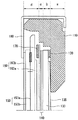
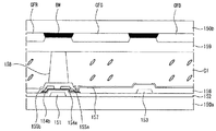
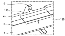
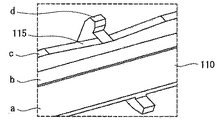
【解決手段】液晶パネルと液晶パネルの下部に位置して光源から出射された光を液晶パネル方向に案内する導光板と、導光板から出射された光を液晶パネルに提供する複数の光学シートを含むバックライトユニットと、液晶パネルとバックライトユニットを収納するように基底面から上部面まで形成された複数の段差部を含み、複数の段差部の中で液晶パネルと対面する段差部が液晶パネルと離隔するようにパターン化された領域を持つメイン支持台を含む。
【選択図】図1
Description
開かれても液晶パネルとメイン支持台110の間に干渉が発生しないので液晶パネル150が破損(割れ)する問題が発生しなくなる。(P2参照)
Claims (10)
- 液晶パネルと、
前記液晶パネルの下部に位置して光源から出射された光を前記液晶パネル方向に案内する導光板と、前記導光板から出射された光を前記液晶パネルに提供する複数の光学シートを含むバックライトユニットと、
前記液晶パネルと前記バックライトユニットを収納するように基底面から上部面まで形成された複数の段差部を含み、前記複数の段差部の中で前記液晶パネルと対面する段差部が前記液晶パネルと離隔するようにパターン化された領域を持つメイン支持台と
を備えた液晶表示装置。 - 前記パターン化された領域は、前記メイン支持台の中央に位置するリブ(rib)部領域である
ことを特徴とする、請求項1記載の液晶表示装置。 - 前記パターン化された領域は、陷沒したパターンを持つ
ことを特徴とする、請求項1記載の液晶表示装置。 - 前記パターン化された領域は、長方形の形状に陷沒した
ことを特徴とする、請求項1記載の液晶表示装置。 - 前記パターン化された領域の周辺領域は、傾いた勾配面を持つ
ことを特徴とする、請求項4記載の液晶表示装置。 - 前記傾いた勾配面の上部角領域は、ラウンド形状を持つ
ことを特徴とする、請求項5記載の液晶表示装置。 - 前記パターン化された領域は、前記パターン化された領域の中心に向けて傾いた勾配面を持つ
ことを特徴とする、請求項1記載の液晶表示装置 - 前記パターン化された領域の幅の広さは、前記液晶パネルと対面する段差部面の幅の広さより狭い
ことを特徴とする、請求項1記載の液晶表示装置。 - 前記液晶パネルと前記複数の光学シートとの間には、
前記液晶パネルの表示領域は露出し非表示領域は遮断するブラックフレ−ムが位置することを含む、請求項1記載の液晶表示装置。 - 前記パターン化された領域の高さは、前記ブラックフレームの高さと同一であるか前記ブラックフレームの高さより低い
ことを特徴とする、請求項9記載の液晶表示装置。
Applications Claiming Priority (2)
| Application Number | Priority Date | Filing Date | Title |
|---|---|---|---|
| KR1020080062853A KR101279119B1 (ko) | 2008-06-30 | 2008-06-30 | 액정표시장치 |
| KR10-2008-0062853 | 2008-06-30 |
Publications (2)
| Publication Number | Publication Date |
|---|---|
| JP2010015124A true JP2010015124A (ja) | 2010-01-21 |
| JP4988691B2 JP4988691B2 (ja) | 2012-08-01 |
Family
ID=41446962
Family Applications (1)
| Application Number | Title | Priority Date | Filing Date |
|---|---|---|---|
| JP2008314669A Expired - Fee Related JP4988691B2 (ja) | 2008-06-30 | 2008-12-10 | 液晶表示装置 |
Country Status (4)
| Country | Link |
|---|---|
| US (1) | US8049831B2 (ja) |
| JP (1) | JP4988691B2 (ja) |
| KR (1) | KR101279119B1 (ja) |
| CN (1) | CN101620339B (ja) |
Cited By (1)
| Publication number | Priority date | Publication date | Assignee | Title |
|---|---|---|---|---|
| JP2014123122A (ja) * | 2012-12-24 | 2014-07-03 | Lg Display Co Ltd | 液晶表示装置および液晶表示装置の製造方法 |
Families Citing this family (17)
| Publication number | Priority date | Publication date | Assignee | Title |
|---|---|---|---|---|
| US8731618B2 (en) * | 2009-04-23 | 2014-05-20 | Apple Inc. | Portable electronic device |
| CN102591045A (zh) * | 2012-02-29 | 2012-07-18 | 深圳市华星光电技术有限公司 | 液晶显示器及其液晶显示装置 |
| KR102066076B1 (ko) * | 2012-12-17 | 2020-01-14 | 엘지디스플레이 주식회사 | 액정표시장치 |
| KR101552762B1 (ko) * | 2013-04-12 | 2015-09-11 | 엘지디스플레이 주식회사 | 액정표시장치 |
| CN103293723B (zh) | 2013-06-26 | 2016-01-06 | 深圳市华星光电技术有限公司 | 一种防止显示模组玻璃面板变形的固定装置 |
| CN103672614B (zh) * | 2013-12-11 | 2017-02-15 | 深圳市华星光电技术有限公司 | 用于曲面液晶显示装置的背光模组以及曲面液晶显示装置 |
| JP2015125182A (ja) | 2013-12-25 | 2015-07-06 | ソニー株式会社 | 表示装置 |
| JP2015129818A (ja) * | 2014-01-06 | 2015-07-16 | パナソニック液晶ディスプレイ株式会社 | 液晶表示装置 |
| TWI569073B (zh) * | 2014-10-27 | 2017-02-01 | 瑞儀光電股份有限公司 | 背光模組及液晶顯示器 |
| KR102227615B1 (ko) * | 2014-11-24 | 2021-03-16 | 엘지디스플레이 주식회사 | 액정표시장치 |
| CN105467678A (zh) * | 2016-01-06 | 2016-04-06 | 京东方科技集团股份有限公司 | 支撑框、显示装置及其装配方法 |
| CN106125405B (zh) * | 2016-09-07 | 2020-11-03 | 海信视像科技股份有限公司 | 一种背光模组及液晶显示装置 |
| KR102662681B1 (ko) * | 2016-12-26 | 2024-04-30 | 엘지디스플레이 주식회사 | 터치 스크린 일체형 표시장치와 그의 제조방법 |
| US10809571B2 (en) * | 2017-01-31 | 2020-10-20 | Sharp Kabushiki Kaisha | Lighting device and display device |
| US11366348B2 (en) * | 2018-08-27 | 2022-06-21 | Lg Display Co., Ltd. | Display device |
| KR102672833B1 (ko) | 2018-08-27 | 2024-06-05 | 엘지디스플레이 주식회사 | 디스플레이 장치 |
| CN113009737B (zh) * | 2019-12-19 | 2022-07-29 | 京东方科技集团股份有限公司 | 背光模组和显示装置 |
Citations (4)
| Publication number | Priority date | Publication date | Assignee | Title |
|---|---|---|---|---|
| JPH0479328U (ja) * | 1990-11-22 | 1992-07-10 | ||
| JP2002108236A (ja) * | 2000-09-28 | 2002-04-10 | Sanyo Electric Co Ltd | 表示装置 |
| JP2005321614A (ja) * | 2004-05-10 | 2005-11-17 | Samsung Electronics Co Ltd | 液晶表示パネル支持体、これを有するバックライトアセンブリ及び液晶表示装置 |
| JP2007047241A (ja) * | 2005-08-08 | 2007-02-22 | Sanyo Epson Imaging Devices Corp | 表示装置 |
Family Cites Families (13)
| Publication number | Priority date | Publication date | Assignee | Title |
|---|---|---|---|---|
| DE69423552T2 (de) * | 1993-08-10 | 2000-09-07 | Canon K.K., Tokio/Tokyo | Flüssigkristallanzeige |
| JP3799829B2 (ja) * | 1997-09-11 | 2006-07-19 | セイコーエプソン株式会社 | 電気光学装置およびその製造方法並びに投射型表示装置 |
| CN2329991Y (zh) * | 1998-03-30 | 1999-07-21 | 金宝电子工业股份有限公司 | 电子器物的防止液晶显示器坠落破裂新型装置 |
| JP2000330096A (ja) * | 1999-05-25 | 2000-11-30 | Nec Corp | 液晶表示装置およびその組立方法 |
| JP2001091945A (ja) * | 1999-09-22 | 2001-04-06 | Advanced Display Inc | 液晶表示装置 |
| KR100640997B1 (ko) * | 2002-12-24 | 2006-11-02 | 엘지.필립스 엘시디 주식회사 | 액정 표시 장치 일체형 터치 패널 |
| JP4564335B2 (ja) * | 2004-11-04 | 2010-10-20 | 東芝モバイルディスプレイ株式会社 | 液晶表示装置 |
| CN1929649A (zh) * | 2005-09-08 | 2007-03-14 | 乐金电子(中国)研究开发中心有限公司 | 移动终端 |
| JP4727383B2 (ja) * | 2005-10-27 | 2011-07-20 | 株式会社 日立ディスプレイズ | 液晶表示装置 |
| KR101177909B1 (ko) * | 2005-11-16 | 2012-08-28 | 엘지디스플레이 주식회사 | 액정 표시 장치용 백라이트 어셈블리 및 이를 이용한 액정표시 모듈 |
| JP4738223B2 (ja) * | 2006-03-24 | 2011-08-03 | 株式会社 日立ディスプレイズ | 表示装置 |
| KR101451737B1 (ko) * | 2006-11-29 | 2014-10-16 | 엘지디스플레이 주식회사 | 액정표시장치 |
| JP2008158432A (ja) * | 2006-12-26 | 2008-07-10 | Hitachi Displays Ltd | 液晶表示装置 |
-
2008
- 2008-06-30 KR KR1020080062853A patent/KR101279119B1/ko not_active Expired - Fee Related
- 2008-12-10 JP JP2008314669A patent/JP4988691B2/ja not_active Expired - Fee Related
- 2008-12-12 CN CN2008101869945A patent/CN101620339B/zh not_active Expired - Fee Related
- 2008-12-30 US US12/318,518 patent/US8049831B2/en not_active Expired - Fee Related
Patent Citations (4)
| Publication number | Priority date | Publication date | Assignee | Title |
|---|---|---|---|---|
| JPH0479328U (ja) * | 1990-11-22 | 1992-07-10 | ||
| JP2002108236A (ja) * | 2000-09-28 | 2002-04-10 | Sanyo Electric Co Ltd | 表示装置 |
| JP2005321614A (ja) * | 2004-05-10 | 2005-11-17 | Samsung Electronics Co Ltd | 液晶表示パネル支持体、これを有するバックライトアセンブリ及び液晶表示装置 |
| JP2007047241A (ja) * | 2005-08-08 | 2007-02-22 | Sanyo Epson Imaging Devices Corp | 表示装置 |
Cited By (1)
| Publication number | Priority date | Publication date | Assignee | Title |
|---|---|---|---|---|
| JP2014123122A (ja) * | 2012-12-24 | 2014-07-03 | Lg Display Co Ltd | 液晶表示装置および液晶表示装置の製造方法 |
Also Published As
| Publication number | Publication date |
|---|---|
| KR20100002816A (ko) | 2010-01-07 |
| CN101620339B (zh) | 2011-04-27 |
| US8049831B2 (en) | 2011-11-01 |
| CN101620339A (zh) | 2010-01-06 |
| US20090322989A1 (en) | 2009-12-31 |
| JP4988691B2 (ja) | 2012-08-01 |
| KR101279119B1 (ko) | 2013-06-26 |
Similar Documents
| Publication | Publication Date | Title |
|---|---|---|
| JP4988691B2 (ja) | 液晶表示装置 | |
| US9482905B2 (en) | Display with column spacer structures | |
| US8982310B2 (en) | Displays with light-curable sealant | |
| KR101331942B1 (ko) | 표시 장치 및 그 제조 방법 | |
| US8520173B2 (en) | Display device | |
| US20090273749A1 (en) | Liquid crystal display device | |
| KR102492032B1 (ko) | 표시 장치 및 이의 제조 방법 | |
| US8400582B2 (en) | Liquid crystal display device and backlight unit | |
| US10690970B2 (en) | Display with hybrid column spacer structures | |
| EP3021161B1 (en) | Curved liquid crystal display device with internal polarisers | |
| WO2017022609A1 (ja) | 表示パネル | |
| KR101717653B1 (ko) | 액정표시패널 | |
| US9275932B2 (en) | Active matrix substrate, and display device | |
| JP5659294B2 (ja) | 表示装置 | |
| US20060028603A1 (en) | Liquid crystal display device and method of fabricating the same | |
| US20190049803A1 (en) | Active switch array substrate, manufacturing method therefor same, and display device using same | |
| US20200110320A1 (en) | Display device | |
| KR20100060380A (ko) | 액정표시장치 | |
| KR101537413B1 (ko) | 액정표시장치 | |
| CN113707668B (zh) | 阵列基板及其制备方法、液晶面板和显示装置 | |
| KR20170061868A (ko) | 미러 디스플레이 패널 | |
| KR101491162B1 (ko) | 액정표시장치 | |
| KR20110077254A (ko) | 횡전계방식 액정표시장치의 제조방법 | |
| KR20110093056A (ko) | 백라이트유닛과 이를 이용한 액정표시장치 | |
| KR20160057228A (ko) | 씨오티 구조 액정표시장치 |
Legal Events
| Date | Code | Title | Description |
|---|---|---|---|
| A131 | Notification of reasons for refusal |
Free format text: JAPANESE INTERMEDIATE CODE: A131 Effective date: 20110705 |
|
| A977 | Report on retrieval |
Free format text: JAPANESE INTERMEDIATE CODE: A971007 Effective date: 20110706 |
|
| A521 | Request for written amendment filed |
Free format text: JAPANESE INTERMEDIATE CODE: A523 Effective date: 20110926 |
|
| TRDD | Decision of grant or rejection written | ||
| A01 | Written decision to grant a patent or to grant a registration (utility model) |
Free format text: JAPANESE INTERMEDIATE CODE: A01 Effective date: 20120410 |
|
| A01 | Written decision to grant a patent or to grant a registration (utility model) |
Free format text: JAPANESE INTERMEDIATE CODE: A01 |
|
| A61 | First payment of annual fees (during grant procedure) |
Free format text: JAPANESE INTERMEDIATE CODE: A61 Effective date: 20120426 |
|
| R150 | Certificate of patent or registration of utility model |
Free format text: JAPANESE INTERMEDIATE CODE: R150 Ref document number: 4988691 Country of ref document: JP Free format text: JAPANESE INTERMEDIATE CODE: R150 |
|
| FPAY | Renewal fee payment (event date is renewal date of database) |
Free format text: PAYMENT UNTIL: 20150511 Year of fee payment: 3 |
|
| R250 | Receipt of annual fees |
Free format text: JAPANESE INTERMEDIATE CODE: R250 |
|
| R250 | Receipt of annual fees |
Free format text: JAPANESE INTERMEDIATE CODE: R250 |
|
| R250 | Receipt of annual fees |
Free format text: JAPANESE INTERMEDIATE CODE: R250 |
|
| R250 | Receipt of annual fees |
Free format text: JAPANESE INTERMEDIATE CODE: R250 |
|
| R250 | Receipt of annual fees |
Free format text: JAPANESE INTERMEDIATE CODE: R250 |
|
| R250 | Receipt of annual fees |
Free format text: JAPANESE INTERMEDIATE CODE: R250 |
|
| LAPS | Cancellation because of no payment of annual fees |