JP2010010580A - Imaging module and method of manufacturing the same, and endoscope apparatus - Google Patents
Imaging module and method of manufacturing the same, and endoscope apparatus Download PDFInfo
- Publication number
- JP2010010580A JP2010010580A JP2008170718A JP2008170718A JP2010010580A JP 2010010580 A JP2010010580 A JP 2010010580A JP 2008170718 A JP2008170718 A JP 2008170718A JP 2008170718 A JP2008170718 A JP 2008170718A JP 2010010580 A JP2010010580 A JP 2010010580A
- Authority
- JP
- Japan
- Prior art keywords
- imaging module
- spacer
- semiconductor chip
- manufacturing
- cover glass
- Prior art date
- Legal status (The legal status is an assumption and is not a legal conclusion. Google has not performed a legal analysis and makes no representation as to the accuracy of the status listed.)
- Granted
Links
Images


Landscapes
- Endoscopes (AREA)
- Solid State Image Pick-Up Elements (AREA)
- Transforming Light Signals Into Electric Signals (AREA)
- Studio Devices (AREA)
Abstract
Description
本発明は、撮像モジュール及びその製造方法並びに内視鏡装置に関する。 The present invention relates to an imaging module, a manufacturing method thereof, and an endoscope apparatus.
デジタルカメラ等に用いられるCCD型やCMOS型等の撮像素子は、特許文献1,2に記載されている様に、撮像素子の受光面上にカバーガラスを若干離間して固定している。このカバーガラスは、撮像素子受光面と平行にした方がよいため、従来は、撮像モジュール製造時に、撮像素子受光面の周囲に複数個のスペーサを配置してその上にカバーガラスを置き、平行度を出すようにしている。
As described in
デジタルカメラ等に用いられる撮像素子と内視鏡装置の挿入部先端に取り付けられる撮像素子とではその大きさが異なり、特に近年の様に細径化が図られた内視鏡装置の先端部に取り付けられる撮像素子は、半導体チップの大きさが2mm角程度の微小な大きさになっている。 The size of the image sensor used in a digital camera or the like is different from that of the image sensor attached to the distal end of the insertion portion of the endoscope device. In particular, the distal end portion of the endoscope device whose diameter has been reduced as in recent years. The attached image sensor has a semiconductor chip with a small size of about 2 mm square.
この様な小さな撮像素子を搭載した撮像モジュールを製造する場合、撮像素子とカバーガラスとの間にスペーサを入れて調節しただけでは、両者間の平行度を出すことができない。つまり、カバーガラスを撮像素子側に押圧する力に偏りが生じると、平行度が違ってきてしまう。 When manufacturing an image pickup module having such a small image pickup device, the degree of parallelism between the two cannot be obtained only by adjusting a spacer between the image pickup device and the cover glass. That is, if the force that presses the cover glass toward the imaging element is biased, the parallelism will be different.
本発明の目的は、カバーガラスと撮像素子との間の平行度を高精度に調整することが可能な撮像モジュールの製造方法及びこの製造方法で製造された撮像モジュールとこの撮像モジュールを搭載した内視鏡装置を提供することにある。 An object of the present invention is to provide an imaging module manufacturing method capable of adjusting the parallelism between the cover glass and the imaging device with high accuracy, an imaging module manufactured by the manufacturing method, and an imaging module mounted therein. An object of the present invention is to provide an endoscope apparatus.
本発明の撮像モジュールは、半導体チップに有効画素領域が形成された撮像素子と、前記半導体チップ上に搭載され前記有効画素領域を囲む枠形状のスペーサと、該スペーサの上に接着されるカバーガラスと、前記半導体チップと前記スペーサとの間を接着する接着材とを備える撮像モジュールであって、前記スペーサに沿う位置の少なくとも3箇所の該スペーサ下部に、夫々圧力センサが設けられていることを特徴とする。 An imaging module of the present invention includes an imaging element in which an effective pixel area is formed on a semiconductor chip, a frame-shaped spacer that is mounted on the semiconductor chip and surrounds the effective pixel area, and a cover glass that is bonded onto the spacer. And an adhesive module for bonding between the semiconductor chip and the spacer, wherein pressure sensors are provided at least under the spacer at three positions along the spacer, respectively. Features.
本発明の撮像モジュールは、前記圧力センサが前記半導体チップの表面部に形成された半導体製の圧力センサであることを特徴とする。 The imaging module of the present invention is characterized in that the pressure sensor is a semiconductor pressure sensor formed on a surface portion of the semiconductor chip.
本発明の撮像モジュールは、前記圧力センサが前記有効画素の製造プロセスで製造されたものであることを特徴とする。 The imaging module of the present invention is characterized in that the pressure sensor is manufactured by a manufacturing process of the effective pixel.
本発明の撮像モジュールの製造方法は、前記接着材の上に前記スペーサを介して載せた前記カバーガラスを前記半導体チップ側に押圧し、複数の前記圧力センサの圧力検出値が同一圧力値になったとき前記接着材を固化させることを特徴とする。尚、ここで、「同一圧力値」とは完全な同一圧力値である必要はなく、製品上、許容精度内,誤差範囲内で同一圧力値であれば良い。 In the method for manufacturing an imaging module according to the present invention, the cover glass placed on the adhesive material via the spacer is pressed toward the semiconductor chip, and the pressure detection values of the plurality of pressure sensors become the same pressure value. And the adhesive is solidified. Here, the “same pressure value” does not need to be a completely identical pressure value, and may be the same pressure value within the allowable accuracy and error range on the product.
本発明の撮像モジュールの製造方法は、接着材が、紫外線硬化樹脂または熱硬化樹脂であることを特徴とする。 The manufacturing method of the imaging module of the present invention is characterized in that the adhesive is an ultraviolet curable resin or a thermosetting resin.
本発明の撮像モジュールの製造方法は、複数の前記撮像素子が形成された半導体ウェハ上に前記スペーサを介して該半導体ウェハと同程度の広さの前記カバーガラスを接着させ、その後に、個々の前記撮像モジュールを個片化することを特徴とする。 In the method for manufacturing an imaging module according to the present invention, the cover glass having the same size as the semiconductor wafer is bonded to the semiconductor wafer on which the plurality of imaging elements are formed via the spacer, The imaging module is singulated.
本発明の内視鏡装置は、上記のいずれかに記載の撮像モジュールを挿入部先端に内蔵したことを特徴とする。 An endoscope apparatus according to the present invention is characterized in that the imaging module according to any one of the above is built in a distal end of an insertion portion.
本発明によれば、カバーガラスと撮像素子との平行度を低コストで精度良く検出し、両者間の平行度を高めた撮像モジュールを製造できるため、高品質の被写体画像を撮影できる撮像モジュールを得ることが可能となる。 According to the present invention, it is possible to manufacture an imaging module that can accurately detect the parallelism between the cover glass and the imaging element at a low cost and can increase the parallelism between the two. Can be obtained.
以下、本発明の一実施形態について、図面を参照して説明する。 Hereinafter, an embodiment of the present invention will be described with reference to the drawings.
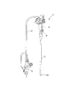
図1は、本発明の一実施形態に係る内視鏡装置の全体図である。この内視鏡装置1は、手元操作部2と、この手元操作部2に連設された挿入部3と、手元操作部2に可撓性チューブ4を介して連設されたコネクタ部5とを備える。
FIG. 1 is an overall view of an endoscope apparatus according to an embodiment of the present invention. The endoscope apparatus 1 includes a
挿入部3の先端部3aの内部には、後述する撮像モジュールが内蔵されており、この撮像モジュールの出力信号線が、挿入部3,手元操作部2,チューブ4と挿通されてコネクタ部5に接続され、このコネクタ部5を、図示省略のビデオプロセッサに連結することで、撮像モジュールによる撮影映像がモニタ表示される。
An imaging module (to be described later) is built in the
図2は、図1に示す先端部3aの前面を示す斜視図である。内視鏡先端部3aには、鉗子孔開口7が設けられており、図1に示す鉗子孔入口8から挿入された図示しない処置具が鉗子孔開口7から出て処置が行われる。
FIG. 2 is a perspective view showing the front surface of the
また、内視鏡先端部3aには、対物レンズ9が設けられ、その両脇に、照明光を出射するライトガイド10,11が設けられている。鉗子孔開口7の脇に設けられた送気送水ノズル12は、対物レンズ9が汚れたとき水等の液体を対物レンズ9に噴射して洗浄を行う。
In addition, an objective lens 9 is provided at the endoscope
近年の内視鏡装置1は、挿入部3の細径化が図られ、その先端部3aの外径が5mm,6mm程度と細くなっている。先端部3aの内部には、鉗子孔開口7の通路やライトガイド10,11の光ファイバ束,送気送水ノズル12への流体通路などが挿通されているため、ここに搭載する撮像モジュールは小型化せざるを得ない。
In the endoscope apparatus 1 in recent years, the diameter of the
図3は、先端部3a内に搭載される撮像装置の概略図である。被写体からの入射光すなわちライトガイド10,11からの照明光の反射光を取り込む対物光学系15の先端部分に図2に示す対物レンズ9が設けられており、対物光学系15の入射光出口端に光路を直角に曲げるプリズム16が設けられ、プリズム16の下端部に平板状の撮像モジュール17が搭載される。
FIG. 3 is a schematic view of an imaging device mounted in the
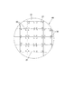
図4は、撮像モジュール17の構成図である。撮像モジュール17は、半導体チップ上に形成した撮像素子21と、撮像素子21の受光面(有効画素領域)の周囲を囲む様に載置した矩形枠形状のスペーサ22と、スペーサ22の上に載置したカバーガラス23と、撮像素子21に隣接配置された端子基板24とを備え、撮像素子21のチップ端部に形成された接続パッド29(図5参照)と端子基板24上の信号端子(図示省略)とがワイヤ25でボンディングされる。
FIG. 4 is a configuration diagram of the
スペーサ22と撮像素子21を形成した半導体チップ表面との間や、カバーガラス23とスペーサ22との間は、例えば紫外線(UV)硬化樹脂により接着される。
The space between the
図5は、撮像モジュール17の上面図であり、図6は、図5のVI―VI線断面である。撮像素子21の中央部分に形成された有効画素領域21aには、図示省略の多数の画素が二次元アレイ状に形成されている。各画素の検出信号を読み出す手段は、CMOS型であればCMOS回路となり、CCD型であれば電荷転送路となるが、本実施形態の撮像素子21はどちらの信号読出手段でも良い。
5 is a top view of the
撮像素子21が形成された半導体チップの有効画素領域21aを囲む4隅近傍位置には、半導体圧力センサ30が設けられている。この半導体圧力センサ30は、例えばピエゾ抵抗効果を利用した拡散型のセンサであり、撮像素子21を形成する半導体プロセスと同一プロセスで半導体チップの表面部に形成される。
そして、有効画素領域21aを囲むように、矩形の枠形状のスペーサ22が半導体チップ上に載置されるが、スペーサ22の4隅が、半導体圧力センサ30上に来るように載置される。更にスペーサ22の上に、透明なカバーガラス23が載置される。スペーサ22の外部には、撮像素子21の接続パッド29の他、圧力センサ30の接続パッド30aも設けられる。
A rectangular frame-
本実施形態に係る撮像モジュールを製造する場合、撮像素子21の半導体チップ上に、スペーサ22をUV硬化樹脂31を薄く塗布してから載せ、その上に、UV硬化樹脂を薄く塗布してカバーガラス23を載せる。このとき、スペーサ22の4隅が、圧力センサ30の上に来るように位置合わせする。
When the imaging module according to the present embodiment is manufactured, the
そして、カバーガラス23の上からカバーガラス23を撮像素子21側に押し、パッド30aを通して得られる各圧力センサ30の検出信号値が同一圧力値を検出した時点で、UV硬化樹脂31に紫外線を照射することで、カバーガラス23,スペーサ22と撮像素子21とを接着し一体化させる。これにより、カバーガラス23と撮像素子の受光面21aとが平行となった撮像モジュールが得られる。
Then, the
スペーサ22の高さは全周に渡って高精度に均一高さに製造されており、4隅の圧力センサ30が許容精度内,誤差範囲内の同一圧力値で押圧されていることを検知した時点で、接着用樹脂を硬化すれば、カバーガラス23と撮像素子21との平行度は高精度に高くなる。
The height of the
本実施形態では、各圧力センサ30を、有効画素を製造するプロセスと同一の半導体プロセスで同一基板上に製造するため、低コストで製造でき、各圧力センサ30間の製造誤差は少なく、このため、圧力検出誤差も極めて小さい。更にカバーガラス23と撮像素子21の平行度を高めたいのであれば、各圧力センサ30の圧力検出誤差を事前に測定しておき、この測定値に基づき補正した検出圧力値で、4つの圧力センサ30の同一圧力を検出するようにすれば良い。
In the present embodiment, since each
図7は、本発明の別実施形態に係る撮像モジュールの製造方法説明図である。図6で説明した実施形態では、1つ1つの撮像モジュール17において、カバーガラス23と撮像素子21との平行度調整を行ってカバーガラス23をスペーサ22を介して撮像素子21に接着した。
FIG. 7 is an explanatory diagram of a method for manufacturing an imaging module according to another embodiment of the present invention. In the embodiment described with reference to FIG. 6, in each of the
しかし、本実施形態では、ウェハ40に複数の撮像素子21を製造し、格子形状のスペーサ連結体を、ウェハ40上に、紫外線硬化樹脂を薄く塗布してから載せ、スペーサ連結体の上にウェハ40と同一径のカバーガラスを載せる。
However, in the present embodiment, a plurality of
ウェハ40上に形成された複数の撮像素子21のうち、離散的な位置の複数個の撮像素子21を選択し、各撮像素子21のいずれかの圧力センサ30(図7中に例示する、点線丸で囲む圧力センサ)の検出値をウェハ40外部で検出できるように配線を行う。この配線は、カバーガラス23をウェハ40に載せる前に行う。
Among the plurality of
そして、スペーサ連結体の上にカバーガラス23を載せで押圧し、検出対象としている圧力センサ30の検出圧力が同一圧力となった時点で、紫外線を照射し樹脂を硬化させる。
Then, the
その後、ウェハ40はカットせずに、その上のスペーサ連結体とカバーガラスだけを、少し幅のあるカッタでダイシングし、次に、このダイシングした跡に沿って、今度は薄いカッタでウェハ40のダイシングを行う。これにより、撮像素子21が個片化される。
Thereafter, the
尚、上述した実施形態では、紫外線硬化樹脂を例に説明したが、熱硬化樹脂を使用して接着することもできる。 In the above-described embodiment, the ultraviolet curable resin is described as an example. However, the thermosetting resin can be used for bonding.
また、半導体チップ表面部に圧力センサ30を形成する例について述べたが、半導体チップ上に圧力センサを形成できない場合には、圧力センサを別途単体で製造し、この圧力センサをスペーサの4隅の下に置いて、上記同様にカバーガラス23と撮像素子21との平行度を検出する様にしても良い。
Moreover, although the example which forms the
また、上述した実施形態では、内視鏡先端部に搭載する撮像モジュールについて説明したが、同じ製造技術を、デジタルカメラ等に搭載する撮像モジュールに適用することも可能である。 In the above-described embodiment, the imaging module mounted on the endoscope distal end has been described. However, the same manufacturing technique can also be applied to an imaging module mounted on a digital camera or the like.
本発明に係る撮像モジュールの製造方法は、低コストで精度良くカバーガラスと撮像素子チップとの平行度を出すことができるため、内視鏡装置に搭載する撮像モジュールに適用すると有用である。 The method for manufacturing an imaging module according to the present invention is useful when applied to an imaging module mounted on an endoscope apparatus because the parallelism between the cover glass and the imaging element chip can be accurately obtained at low cost.
1 内視鏡装置
3 挿入部
3a 挿入部先端(内視鏡先端)
9 対物レンズ
15 対物光学系
16 プリズム
17 撮像モジュール
21 撮像素子
22 スペーサ
23 カバーガラス
30 圧力センサ
31 接着用樹脂
40 半導体ウェハ
DESCRIPTION OF SYMBOLS 1
DESCRIPTION OF SYMBOLS 9
Claims (7)
Priority Applications (1)
| Application Number | Priority Date | Filing Date | Title |
|---|---|---|---|
| JP2008170718A JP5186295B2 (en) | 2008-06-30 | 2008-06-30 | Imaging module, method for manufacturing the same, and endoscope apparatus |
Applications Claiming Priority (1)
| Application Number | Priority Date | Filing Date | Title |
|---|---|---|---|
| JP2008170718A JP5186295B2 (en) | 2008-06-30 | 2008-06-30 | Imaging module, method for manufacturing the same, and endoscope apparatus |
Publications (2)
| Publication Number | Publication Date |
|---|---|
| JP2010010580A true JP2010010580A (en) | 2010-01-14 |
| JP5186295B2 JP5186295B2 (en) | 2013-04-17 |
Family
ID=41590680
Family Applications (1)
| Application Number | Title | Priority Date | Filing Date |
|---|---|---|---|
| JP2008170718A Expired - Fee Related JP5186295B2 (en) | 2008-06-30 | 2008-06-30 | Imaging module, method for manufacturing the same, and endoscope apparatus |
Country Status (1)
| Country | Link |
|---|---|
| JP (1) | JP5186295B2 (en) |
Families Citing this family (1)
| Publication number | Priority date | Publication date | Assignee | Title |
|---|---|---|---|---|
| US6878206B2 (en) | 2001-07-16 | 2005-04-12 | Applied Materials, Inc. | Lid assembly for a processing system to facilitate sequential deposition techniques |
Citations (4)
| Publication number | Priority date | Publication date | Assignee | Title |
|---|---|---|---|---|
| JP2002270802A (en) * | 2001-03-06 | 2002-09-20 | Canon Inc | Solid-state imaging device and its manufacturing method |
| JP2003303946A (en) * | 2002-04-12 | 2003-10-24 | Sony Corp | Solid-state image pickup device and manufacturing method thereof |
| JP2005501405A (en) * | 2001-08-24 | 2005-01-13 | カール−ツアイス−シュティフツンク | Manufacturing method of electronic parts |
| JP2006147864A (en) * | 2004-11-19 | 2006-06-08 | Fujikura Ltd | Semiconductor package and its manufacturing method |
-
2008
- 2008-06-30 JP JP2008170718A patent/JP5186295B2/en not_active Expired - Fee Related
Patent Citations (4)
| Publication number | Priority date | Publication date | Assignee | Title |
|---|---|---|---|---|
| JP2002270802A (en) * | 2001-03-06 | 2002-09-20 | Canon Inc | Solid-state imaging device and its manufacturing method |
| JP2005501405A (en) * | 2001-08-24 | 2005-01-13 | カール−ツアイス−シュティフツンク | Manufacturing method of electronic parts |
| JP2003303946A (en) * | 2002-04-12 | 2003-10-24 | Sony Corp | Solid-state image pickup device and manufacturing method thereof |
| JP2006147864A (en) * | 2004-11-19 | 2006-06-08 | Fujikura Ltd | Semiconductor package and its manufacturing method |
Also Published As
| Publication number | Publication date |
|---|---|
| JP5186295B2 (en) | 2013-04-17 |
Similar Documents
| Publication | Publication Date | Title |
|---|---|---|
| JP5047679B2 (en) | Imaging unit and method for manufacturing the imaging unit | |
| US10571680B2 (en) | Image pickup apparatus and endoscope | |
| US9681067B2 (en) | Manufacturing method for image pickup unit and image pickup unit | |
| JP4754221B2 (en) | Optical lens alignment assembly for centering the optical lens on the image sensor | |
| US20100091168A1 (en) | Solid-state image pickup apparatus, and method of manufacturing solid-state image pickup apparatus | |
| US8796798B2 (en) | Imaging module, fabricating method therefor, and imaging device | |
| JP5676171B2 (en) | Solid-state imaging device, manufacturing method thereof, and electronic apparatus | |
| CN103492927A (en) | Image pickup mechanism, endoscope, and method of manufacturing an image pickup mechanism | |
| JP4819152B2 (en) | Optical element wafer, optical element wafer module, optical element module, method for manufacturing optical element module, electronic element wafer module, method for manufacturing electronic element module, electronic element module, and electronic information device | |
| KR20180034329A (en) | Laminated lens structure, method of manufacturing the same, and electronic device | |
| US7998779B2 (en) | Solid-state imaging device and method of fabricating solid-state imaging device | |
| WO2017061296A1 (en) | Solid-state imaging element package, manufacturing method therefor, and electronic device | |
| JP2008528094A (en) | Sensor with narrow assembly outline | |
| JP2004080774A (en) | Method of manufacturing image sensors module | |
| JP4772826B2 (en) | Imaging device | |
| JP2011100971A (en) | Method for manufacturing curved circuit | |
| US7785915B2 (en) | Wafer level method of locating focal plane of imager devices | |
| JP5186295B2 (en) | Imaging module, method for manufacturing the same, and endoscope apparatus | |
| US10739576B2 (en) | Imaging apparatus, endoscopic system, and imaging apparatus manufacturing method | |
| US10542874B2 (en) | Imaging device and endoscope device | |
| EP3712966B1 (en) | Method for manufacturing a curved-surface detector | |
| US20100225799A1 (en) | Image pickup unit, method of manufacturing image pickup unit and electronic apparatus provided with image pickup unit | |
| JP4938936B2 (en) | Solid-state imaging device | |
| JP2010010579A (en) | Imaging module and method of manufacturing the same, and endoscope apparatus | |
| JP6415129B2 (en) | Imaging device |
Legal Events
| Date | Code | Title | Description |
|---|---|---|---|
| A711 | Notification of change in applicant |
Free format text: JAPANESE INTERMEDIATE CODE: A711 Effective date: 20100618 |
|
| A621 | Written request for application examination |
Free format text: JAPANESE INTERMEDIATE CODE: A621 Effective date: 20110208 |
|
| RD04 | Notification of resignation of power of attorney |
Free format text: JAPANESE INTERMEDIATE CODE: A7424 Effective date: 20111216 |
|
| RD03 | Notification of appointment of power of attorney |
Free format text: JAPANESE INTERMEDIATE CODE: A7423 Effective date: 20120914 |
|
| RD04 | Notification of resignation of power of attorney |
Free format text: JAPANESE INTERMEDIATE CODE: A7424 Effective date: 20121004 |
|
| TRDD | Decision of grant or rejection written | ||
| A01 | Written decision to grant a patent or to grant a registration (utility model) |
Free format text: JAPANESE INTERMEDIATE CODE: A01 Effective date: 20121225 |
|
| A977 | Report on retrieval |
Free format text: JAPANESE INTERMEDIATE CODE: A971007 Effective date: 20121227 |
|
| A61 | First payment of annual fees (during grant procedure) |
Free format text: JAPANESE INTERMEDIATE CODE: A61 Effective date: 20130121 |
|
| R150 | Certificate of patent or registration of utility model |
Free format text: JAPANESE INTERMEDIATE CODE: R150 |
|
| FPAY | Renewal fee payment (event date is renewal date of database) |
Free format text: PAYMENT UNTIL: 20160125 Year of fee payment: 3 |
|
| LAPS | Cancellation because of no payment of annual fees |