JP2010010558A - Light-emitting device, and method of manufacturing light-emitting device - Google Patents
Light-emitting device, and method of manufacturing light-emitting device Download PDFInfo
- Publication number
- JP2010010558A JP2010010558A JP2008170388A JP2008170388A JP2010010558A JP 2010010558 A JP2010010558 A JP 2010010558A JP 2008170388 A JP2008170388 A JP 2008170388A JP 2008170388 A JP2008170388 A JP 2008170388A JP 2010010558 A JP2010010558 A JP 2010010558A
- Authority
- JP
- Japan
- Prior art keywords
- light emitting
- wiring pattern
- insulating layer
- metal substrate
- emitting element
- Prior art date
- Legal status (The legal status is an assumption and is not a legal conclusion. Google has not performed a legal analysis and makes no representation as to the accuracy of the status listed.)
- Granted
Links
- 238000004519 manufacturing process Methods 0.000 title claims abstract description 17
- 239000002184 metal Substances 0.000 claims abstract description 85
- 229910052751 metal Inorganic materials 0.000 claims abstract description 85
- 239000000758 substrate Substances 0.000 claims abstract description 60
- 238000000034 method Methods 0.000 claims abstract description 30
- 238000007747 plating Methods 0.000 claims abstract description 23
- 238000009713 electroplating Methods 0.000 claims abstract description 11
- 238000002360 preparation method Methods 0.000 claims abstract description 7
- 238000005530 etching Methods 0.000 claims description 6
- 230000015556 catabolic process Effects 0.000 abstract 1
- 238000009413 insulation Methods 0.000 description 7
- 239000010949 copper Substances 0.000 description 4
- 239000000463 material Substances 0.000 description 4
- 239000004593 Epoxy Substances 0.000 description 3
- PXHVJJICTQNCMI-UHFFFAOYSA-N Nickel Chemical compound [Ni] PXHVJJICTQNCMI-UHFFFAOYSA-N 0.000 description 3
- 239000011521 glass Substances 0.000 description 3
- 239000010931 gold Substances 0.000 description 3
- 230000017525 heat dissipation Effects 0.000 description 3
- 239000000243 solution Substances 0.000 description 3
- 238000003466 welding Methods 0.000 description 3
- RYGMFSIKBFXOCR-UHFFFAOYSA-N Copper Chemical compound [Cu] RYGMFSIKBFXOCR-UHFFFAOYSA-N 0.000 description 2
- 239000007864 aqueous solution Substances 0.000 description 2
- 229910052802 copper Inorganic materials 0.000 description 2
- 229910052737 gold Inorganic materials 0.000 description 2
- 229920002120 photoresistant polymer Polymers 0.000 description 2
- 239000011347 resin Substances 0.000 description 2
- 229920005989 resin Polymers 0.000 description 2
- BQCADISMDOOEFD-UHFFFAOYSA-N Silver Chemical compound [Ag] BQCADISMDOOEFD-UHFFFAOYSA-N 0.000 description 1
- 239000000853 adhesive Substances 0.000 description 1
- 230000001070 adhesive effect Effects 0.000 description 1
- 239000000919 ceramic Substances 0.000 description 1
- 239000004020 conductor Substances 0.000 description 1
- ORTQZVOHEJQUHG-UHFFFAOYSA-L copper(II) chloride Chemical compound Cl[Cu]Cl ORTQZVOHEJQUHG-UHFFFAOYSA-L 0.000 description 1
- 238000010586 diagram Methods 0.000 description 1
- 230000000694 effects Effects 0.000 description 1
- PCHJSUWPFVWCPO-UHFFFAOYSA-N gold Chemical compound [Au] PCHJSUWPFVWCPO-UHFFFAOYSA-N 0.000 description 1
- 230000020169 heat generation Effects 0.000 description 1
- FBAFATDZDUQKNH-UHFFFAOYSA-M iron chloride Chemical compound [Cl-].[Fe] FBAFATDZDUQKNH-UHFFFAOYSA-M 0.000 description 1
- 229910021645 metal ion Inorganic materials 0.000 description 1
- 238000012986 modification Methods 0.000 description 1
- 230000004048 modification Effects 0.000 description 1
- 229910052759 nickel Inorganic materials 0.000 description 1
- ORQBXQOJMQIAOY-UHFFFAOYSA-N nobelium Chemical compound [No] ORQBXQOJMQIAOY-UHFFFAOYSA-N 0.000 description 1
- 229910052709 silver Inorganic materials 0.000 description 1
- 239000004332 silver Substances 0.000 description 1
Images

Classifications
-
- H—ELECTRICITY
- H01—ELECTRIC ELEMENTS
- H01L—SEMICONDUCTOR DEVICES NOT COVERED BY CLASS H10
- H01L2224/00—Indexing scheme for arrangements for connecting or disconnecting semiconductor or solid-state bodies and methods related thereto as covered by H01L24/00
- H01L2224/01—Means for bonding being attached to, or being formed on, the surface to be connected, e.g. chip-to-package, die-attach, "first-level" interconnects; Manufacturing methods related thereto
- H01L2224/42—Wire connectors; Manufacturing methods related thereto
- H01L2224/47—Structure, shape, material or disposition of the wire connectors after the connecting process
- H01L2224/48—Structure, shape, material or disposition of the wire connectors after the connecting process of an individual wire connector
- H01L2224/4805—Shape
- H01L2224/4809—Loop shape
- H01L2224/48091—Arched
Abstract
Description
本発明は発光素子が搭載された金属基板を有する発光装置、及び発光装置の製造方法に関する。 The present invention relates to a light emitting device having a metal substrate on which a light emitting element is mounted, and a method for manufacturing the light emitting device.
発光素子を有する発光装置では、発光素子の発光とともに熱が発生する。この熱によって、発光素子の発光効率や寿命は低下する。特に、発光素子が発光ダイオード(LED)である場合、発熱による発光効率の低下、及び寿命の低下は顕著である。 In a light-emitting device having a light-emitting element, heat is generated as the light-emitting element emits light. This heat reduces the light emission efficiency and life of the light emitting element. In particular, when the light-emitting element is a light-emitting diode (LED), a decrease in light emission efficiency and a decrease in life due to heat generation are significant.
したがって、発光時の熱を効率よく放熱することが重要である。放熱の効果を上げる一手段として、金属基板に発光素子を配置する手段がある(例えば、特許文献1〜3参照。)。金属基板は熱伝導率が高いため、放熱性に長けている。 Therefore, it is important to efficiently dissipate heat during light emission. As a means for improving the heat dissipation effect, there is a means for arranging a light emitting element on a metal substrate (see, for example, Patent Documents 1 to 3). Since the metal substrate has a high thermal conductivity, it is excellent in heat dissipation.
金属基板を用いた発光装置では、一般に、金属基板の一面に絶縁層が形成されており、当該絶縁層の表面に配線パターンが形成されている。発光素子は、この配線パターンに電気的に接続されている。 In a light emitting device using a metal substrate, an insulating layer is generally formed on one surface of the metal substrate, and a wiring pattern is formed on the surface of the insulating layer. The light emitting element is electrically connected to this wiring pattern.
発光素子と配線パターンとを電気的に接続する手段として、導電性のワイヤを用いて結線する手段(ワイヤボンディング)が挙げられる。ワイヤボンディングによって、発光素子と配線パターンとを電気的に接続するためには、配線パターンの表面に、導電性のワイヤと容易に溶着可能な金属を形成しておくことが好ましい。配線パターンの表面の金属は、めっき法によって容易に形成することができる(特許文献1及び2参照。)。 Examples of means for electrically connecting the light emitting element and the wiring pattern include means for connecting using a conductive wire (wire bonding). In order to electrically connect the light emitting element and the wiring pattern by wire bonding, it is preferable to form a metal that can be easily welded to the conductive wire on the surface of the wiring pattern. The metal on the surface of the wiring pattern can be easily formed by a plating method (see Patent Documents 1 and 2).
特許文献3では、LEDが接続されるパターン配線が形成される絶縁基材の外形を、金属基板の外形よりも大きくすることが記載されている。これにより、金属基板の端面から絶縁基材の表面を経て配線パターンに到達するまでの最短距離(絶縁距離)を長くすることができる。
特許文献1及び2に記載の発光装置では、配線パターンの表面にめっき金属が形成されている。めっき金属は電解めっき法を用いることで容易に形成することができる。電解めっき法を実施する際に、配線パターンに電流を供給する。そのため、配線パターンの一端は、通常、絶縁層の端辺まで延びている。 In the light emitting devices described in Patent Documents 1 and 2, a plated metal is formed on the surface of the wiring pattern. The plated metal can be easily formed by using an electrolytic plating method. When performing the electrolytic plating method, a current is supplied to the wiring pattern. Therefore, one end of the wiring pattern usually extends to the end side of the insulating layer.
したがって、電解めっき法でめっき金属を形成する場合、配線パターンの一端から絶縁層の表面を経て金属基板に達するまでの最短距離(絶縁距離)は、絶縁層の厚みと等しくなる。このように絶縁距離が短いと、発光装置の耐電圧が低下するという問題がある。 Therefore, when forming the plating metal by the electrolytic plating method, the shortest distance (insulation distance) from one end of the wiring pattern to the metal substrate through the surface of the insulating layer is equal to the thickness of the insulating layer. Thus, when the insulation distance is short, there is a problem that the withstand voltage of the light emitting device is lowered.
また、特許文献3に記載の発光装置においても、仮に、配線パターンの表面に電解めっき法でめっき金属を形成する場合には、一端が絶縁基材の端辺まで延びている配線パターンが必要である。この場合、金属基板と配線パターンとの絶縁距離は短くなり、発光装置の耐電圧は低下する。 Also, in the light emitting device described in Patent Document 3, if a plated metal is formed on the surface of the wiring pattern by an electrolytic plating method, a wiring pattern in which one end extends to the edge of the insulating base material is necessary. is there. In this case, the insulation distance between the metal substrate and the wiring pattern is shortened, and the withstand voltage of the light emitting device is reduced.
本発明の目的は上記背景技術の課題に鑑み、耐電圧が向上する発光装置、及びその発光装置の製造方法を提供することである。 An object of the present invention is to provide a light-emitting device with improved withstand voltage and a method for manufacturing the light-emitting device in view of the problems of the background art.
上記目的を達成するため本発明は、発光素子が搭載された金属基板を有する発光装置の製造方法であって、準備工程と、配線パターン形成工程と、めっき工程と、除去工程と、発光素子搭載工程と、を有している。準備工程では、一面に絶縁層が形成された金属基板であって、該金属基板の少なくとも端辺に絶縁層の端辺が接している金属基板を準備する。配線パターン形成工程では、絶縁層の金属基板と反対側の面に、一端が絶縁層の端辺まで延びている配線パターンを形成する。めっき工程では、電解めっき法によって、配線パターンの表面にめっき金属を形成する。除去工程では、配線パターンの一端から絶縁層の表面を経て金属基板の端面に到達するまでの最短距離が絶縁層の厚みよりも長くなるように、配線パターンの一端側を除去する。発光素子搭載工程では、発光素子を搭載し、発光素子と配線パターンとを、電気的に接続する。 In order to achieve the above object, the present invention is a method of manufacturing a light emitting device having a metal substrate on which a light emitting element is mounted, comprising a preparation step, a wiring pattern forming step, a plating step, a removing step, and a light emitting device mounting. And a process. In the preparation step, a metal substrate having an insulating layer formed on one surface and having an edge of the insulating layer in contact with at least an edge of the metal substrate is prepared. In the wiring pattern forming step, a wiring pattern having one end extending to the edge of the insulating layer is formed on the surface of the insulating layer opposite to the metal substrate. In the plating step, a plating metal is formed on the surface of the wiring pattern by electrolytic plating. In the removing step, one end side of the wiring pattern is removed so that the shortest distance from one end of the wiring pattern to the end surface of the metal substrate through the surface of the insulating layer is longer than the thickness of the insulating layer. In the light emitting element mounting step, the light emitting element is mounted, and the light emitting element and the wiring pattern are electrically connected.
また、本発明の発光装置は、一面に絶縁層が形成された金属基板であって、該金属基板の少なくとも端辺に前記絶縁層の端辺が接している金属基板と、絶縁層の金属基板と反対側の面に形成された配線パターンと、配線パターンに接続された発光素子と、を備えている。配線パターンの表面には、電解めっき法によるめっき金属が形成されている。そして、配線パターンの一端から絶縁層の表面を経て金属基板の端面に到達するまでの最短距離が絶縁層の厚みよりも長いことを特徴とする。 The light-emitting device of the present invention is a metal substrate having an insulating layer formed on one surface, the metal substrate having at least the edge of the metal substrate in contact with the end of the insulating layer, and the metal substrate of the insulating layer. And a light emitting element connected to the wiring pattern. On the surface of the wiring pattern, a plating metal is formed by an electrolytic plating method. The shortest distance from one end of the wiring pattern to the end surface of the metal substrate through the surface of the insulating layer is longer than the thickness of the insulating layer.
本発明によれば、発光装置の耐電圧を向上させることができる。 According to the present invention, the withstand voltage of the light emitting device can be improved.
以下、本発明の実施形態について図面を参照して説明する。 Embodiments of the present invention will be described below with reference to the drawings.
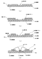
図1は、本発明の一実施形態に係る発光装置の模式的断面図である。本実施形態に係る発光装置は、発光素子101と金属基板102とを有している。発光素子101としては、例えば発光ダイオード(LED)を好適に用いることができる。 FIG. 1 is a schematic cross-sectional view of a light emitting device according to an embodiment of the present invention. The light emitting device according to this embodiment includes a light emitting element 101 and a metal substrate 102. As the light emitting element 101, for example, a light emitting diode (LED) can be suitably used.
金属基板102の一面には絶縁層103が形成されている。絶縁層103の端辺は、金属基板102の少なくとも端辺に接している。絶縁層103は開口部103bを有しており、開口部103bから金属基板102の一部が露出している。
An
発光素子101は、この開口部103bから露出している金属基板102に配置されている。金属基板102は、発光素子101の発熱を効果的に放熱することができれば、どのような金属であっても良い。 The light emitting element 101 is disposed on the metal substrate 102 exposed from the opening 103b. The metal substrate 102 may be any metal as long as it can effectively dissipate heat generated by the light emitting element 101.
絶縁層103の金属基板102と反対側の面には、配線パターン104が形成されている。発光素子101は、導電性のワイヤ105によって、配線パターン104と接続されている。また、配線パターン104の表面には、めっき金属(不図示)が電解めっき法によって形成されている。めっき金属は、ワイヤ105を溶着するために形成されている。
A
本実施例における発光装置では、配線パターン104の一端が絶縁層103の端辺103aまで延びていない。
In the light emitting device in this embodiment, one end of the
本構成によれば、配線パターン104の一端が絶縁層103の表面を経て金属基板102の端面102aに到達するまでの最短距離(以下、絶縁距離と呼ぶ。)が絶縁層103の厚みよりも長くなる。このように、絶縁距離が長くなるため、発光装置の耐電圧は向上し、それによって発光装置の信頼性が向上する。
According to this configuration, the shortest distance (hereinafter referred to as an insulation distance) until one end of the
さらに、発光素子101とワイヤ105は、樹脂(不図示)で封止されていることが好ましい。これにより、発光素子101を保護し、発光素子101の光利用効率を向上することができる。また、発光素子101に電力を供給するための電源(不図示)は、配線パターン104に電気的に接続されている。
Furthermore, the light emitting element 101 and the wire 105 are preferably sealed with a resin (not shown). Thereby, the light emitting element 101 can be protected and the light utilization efficiency of the light emitting element 101 can be improved. A power source (not shown) for supplying power to the light emitting element 101 is electrically connected to the
次に、本発明の一実施形態に係る発光装置の製造方法について説明する。図2(a)〜(d)は、本実施形態に係る発光装置の製造方法を説明する工程図である。 Next, a method for manufacturing a light emitting device according to an embodiment of the present invention will be described. 2A to 2D are process diagrams illustrating a method for manufacturing a light emitting device according to this embodiment.
発光装置の製造方法は、準備工程と、配線パターン形成工程と、めっき工程と、除去工程と、発光素子搭載工程と、を有している。 The method for manufacturing a light emitting device includes a preparation process, a wiring pattern forming process, a plating process, a removing process, and a light emitting element mounting process.
準備工程では、一面に絶縁層103が形成された金属基板102を準備する。金属基板102の少なくとも端辺に絶縁層103の端辺が接している(図2(a)参照。)。
絶縁層103としては、プリプレグ、ガラスエポキシ板、セラミックなどを用いることができる。絶縁層103としてガラスエポキシ板を用いる場合、ガラスエポキシ板は、接着剤によって金属基板102に接着することができる。
In the preparation step, a metal substrate 102 having an
As the
絶縁層103は、金属基板102の一部が露出するように、開口部103bを有していることが好ましい。この場合、開口部103bから露出している金属基板102に、発光素子を配置することができるため、発光素子の放熱性が向上する。
The insulating
配線パターン形成工程では、一端が絶縁層103の端辺103aまで延びている配線パターン104を、絶縁層103の金属基板102と反対側の面に形成する(図2(b)参照。)。配線パターン104は、発光素子101に電力を供給するための配線である。
In the wiring pattern forming step, a
配線パターン104は、電気伝導性が高い材料から構成されていれば良い。一般的には、配線パターン104は銅(Cu)から構成される。配線パターン104は任意の公知技術を利用して形成することができる。その一例として、フォトリゾグラフィー法を挙げることが出来る。
The
めっき工程では、電解めっき法によって配線パターン104の表面にめっき金属(不図示)を形成する。このとき、金属イオンを含む溶液中で、一端が絶縁層103の端辺103aまで延びている配線パターン104に電流を供給することで、配線パターン104の表面にめっき金属を形成することができる。めっき金属は、後述のワイヤ105を溶着させて、配線パターン104と接続するために形成する。
In the plating step, a plating metal (not shown) is formed on the surface of the
また、絶縁層103の開口部103bから露出した金属基板102に発光素子101を搭載する場合、めっき工程において、開口部103bから露出している金属基板102にもめっき金属を形成することが好ましい。これにより、めっき金属に発光素子101を溶着することで、容易に発光素子101を搭載することができる。
In the case where the light emitting element 101 is mounted on the metal substrate 102 exposed from the opening 103b of the insulating
めっき金属の金属種としては、金(Au)、銀(Ag)、ニッケル(Ni)などを用いることができる。めっき金属の金属種は、溶着する金属の種類に応じて、適宜決めれば良い。 Gold (Au), silver (Ag), nickel (Ni), etc. can be used as the metal species of the plating metal. What is necessary is just to determine the metal seed | species of a plating metal suitably according to the kind of metal to weld.
除去工程では、絶縁層103の端辺103aまで延びている配線パターン104aの一端側を、エッチングにより除去する(図2(c)参照。)。
In the removing step, one end side of the wiring pattern 104a extending to the
除去工程の一例として、絶縁層103に耐エッチング性を有するマスクを形成し、配線パターン104の一端から絶縁層103の表面を経て金属基板102の端面102aに到達するまでの最短距離が絶縁層103の厚みよりも長くなるように、配線パターン104の一端側をエッチング液によって除去する。つまり、配線パターン104が絶縁層103の端辺103aに到達しないように、配線パターン104を形成する。
As an example of the removal process, a mask having etching resistance is formed on the insulating
エッチング液はエッチングで除去する材質によって決定する。例えば、配線パターン104が銅(Cu)から成る場合、エッチング液としては、塩化鉄水溶液や塩化銅水溶液などを用いることができる。また、マスクとしては、フォトレジストを用いることができる。フォトレジストはネガ型、ポジ型のどちらであって良い。
The etchant is determined by the material to be removed by etching. For example, when the
このように、絶縁層103の端辺103a近傍に位置している配線パターン104を除去することで、絶縁距離が長くなるため、発光装置の耐電圧は向上する。したがって、発光装置の信頼性は向上する。
In this manner, by removing the
発光素子搭載工程では、発光素子101を、ワイヤボンディングによって、配線パターン104と電気的に接続する(図2(d)参照。)。このとき、配線パターン104の表面に形成されているめっき金属を、熱や超音波によって溶解させて、導電性のワイヤ105を溶着させる。
In the light emitting element mounting step, the light emitting element 101 is electrically connected to the
このようにして、耐電圧を向上させた発光装置を製造することができる。発光素子101と配線パターン104とを接続するワイヤ105は、例えばAuやAlなどの導電性の材料から構成される。
In this manner, a light emitting device with improved withstand voltage can be manufactured. The wire 105 that connects the light emitting element 101 and the
発光素子101は、金属基板102上に搭載されることが好ましい。具体的には、絶縁層103の開口部103bから露出している金属基板102に、発光素子101を配置することが好ましい。これにより、発光素子101が発生する熱を効果的に放熱することができる。
The light emitting element 101 is preferably mounted on the metal substrate 102. Specifically, the light-emitting element 101 is preferably disposed on the metal substrate 102 exposed from the opening 103b of the insulating
また、発光素子101とワイヤ105とを、樹脂(不図示)で封止しても良い。これにより、発光素子101を保護し、発光素子101の光利用効率を向上することができる。 Further, the light emitting element 101 and the wire 105 may be sealed with a resin (not shown). Thereby, the light emitting element 101 can be protected and the light utilization efficiency of the light emitting element 101 can be improved.
金属基板102に搭載される発光素子101は1つに限らず、複数であっても良い。また、発光素子101を金属基板102に搭載する方法や位置などは、上記構成によらず、種々変更可能である。 The number of light-emitting elements 101 mounted on the metal substrate 102 is not limited to one, and may be plural. Further, the method and position of mounting the light emitting element 101 on the metal substrate 102 can be variously changed regardless of the above configuration.
以上、本発明の望ましい実施形態について提示し、詳細に説明したが、本発明は上記実施形態に限定されるものではなく、要旨を逸脱しない限り、さまざまな変更及び修正が可能であることを理解されたい。 Although the preferred embodiments of the present invention have been presented and described in detail above, the present invention is not limited to the above-described embodiments, and it is understood that various changes and modifications can be made without departing from the gist. I want to be.
101 発光素子
102 金属基板
102a 端面
103 絶縁層
103a 端辺
103b 開口部
104 配線パターン
105 ワイヤ
DESCRIPTION OF SYMBOLS 101 Light emitting element 102
Claims (10)
一面に絶縁層が形成された金属基板であって、該金属基板の少なくとも端辺に前記絶縁層の端辺が接している前記金属基板を準備する準備工程と、
前記絶縁層の前記金属基板と反対側の面に、一端が前記絶縁層の端辺まで延びている配線パターンを形成する配線パターン形成工程と、
電解めっき法によって、前記配線パターンの表面にめっき金属を形成するめっき工程と、
前記配線パターンの一端から前記絶縁層の表面を経て前記金属基板の端面に到達するまでの最短距離が前記絶縁層の厚みよりも長くなるように、前記配線パターンの一端側を除去する除去工程と、
前記発光素子を搭載し、前記発光素子と前記配線パターンとを、電気的に接続する発光素子搭載工程と、を有する発光装置の製造方法。 A method of manufacturing a light emitting device having a metal substrate on which a light emitting element is mounted,
A preparation step of preparing a metal substrate having an insulating layer formed on one surface, wherein the metal substrate is in contact with at least an edge of the metal substrate;
A wiring pattern forming step of forming a wiring pattern having one end extending to an end side of the insulating layer on the surface of the insulating layer opposite to the metal substrate;
A plating step of forming a plating metal on the surface of the wiring pattern by electrolytic plating;
A removing step of removing one end side of the wiring pattern so that the shortest distance from one end of the wiring pattern to the end surface of the metal substrate through the surface of the insulating layer is longer than the thickness of the insulating layer; ,
A method for manufacturing a light emitting device, comprising: mounting the light emitting element; and a step of mounting the light emitting element to electrically connect the light emitting element and the wiring pattern.
前記発光素子搭載工程において、前記開口部から露出している前記金属基板に前記発光素子を配置する、請求項1から4のいずれか1項に記載の発光装置の製造方法。 The insulating layer has an opening so that a part of the metal substrate is exposed,
5. The method for manufacturing a light emitting device according to claim 1, wherein, in the light emitting element mounting step, the light emitting element is arranged on the metal substrate exposed from the opening.
前記配線パターンの一端から前記絶縁層の表面を経て前記金属基板の端面に到達するまでの最短距離が前記絶縁層の厚みよりも長いことを特徴とする、発光装置。 A metal substrate having an insulating layer formed on one surface thereof, wherein the metal substrate is in contact with at least an edge of the metal substrate, and the surface of the insulating layer opposite to the metal substrate; In a light emitting device comprising a formed wiring pattern and a light emitting element connected to the wiring pattern, wherein a plating metal is formed on the surface of the wiring pattern by an electrolytic plating method,
The light emitting device characterized in that the shortest distance from one end of the wiring pattern to the end surface of the metal substrate through the surface of the insulating layer is longer than the thickness of the insulating layer.
前記開口部から露出している前記金属基板に前記発光素子が配置されていることを特徴とする、請求項7または8に記載の発光装置。 The insulating layer has an opening so that a part of the metal substrate is exposed,
The light emitting device according to claim 7, wherein the light emitting element is disposed on the metal substrate exposed from the opening.
Priority Applications (1)
| Application Number | Priority Date | Filing Date | Title |
|---|---|---|---|
| JP2008170388A JP5408583B2 (en) | 2008-06-30 | 2008-06-30 | LIGHT EMITTING DEVICE AND LIGHT EMITTING DEVICE MANUFACTURING METHOD |
Applications Claiming Priority (1)
| Application Number | Priority Date | Filing Date | Title |
|---|---|---|---|
| JP2008170388A JP5408583B2 (en) | 2008-06-30 | 2008-06-30 | LIGHT EMITTING DEVICE AND LIGHT EMITTING DEVICE MANUFACTURING METHOD |
Related Child Applications (1)
| Application Number | Title | Priority Date | Filing Date |
|---|---|---|---|
| JP2013167996A Division JP2013229639A (en) | 2013-08-13 | 2013-08-13 | Light-emitting device and method for manufacturing the same |
Publications (2)
| Publication Number | Publication Date |
|---|---|
| JP2010010558A true JP2010010558A (en) | 2010-01-14 |
| JP5408583B2 JP5408583B2 (en) | 2014-02-05 |
Family
ID=41590662
Family Applications (1)
| Application Number | Title | Priority Date | Filing Date |
|---|---|---|---|
| JP2008170388A Active JP5408583B2 (en) | 2008-06-30 | 2008-06-30 | LIGHT EMITTING DEVICE AND LIGHT EMITTING DEVICE MANUFACTURING METHOD |
Country Status (1)
| Country | Link |
|---|---|
| JP (1) | JP5408583B2 (en) |
Cited By (2)
| Publication number | Priority date | Publication date | Assignee | Title |
|---|---|---|---|---|
| JP2012004595A (en) * | 2011-09-21 | 2012-01-05 | Toshiba Corp | Method of manufacturing light-emitting element module substrate |
| KR101773045B1 (en) * | 2011-01-21 | 2017-08-30 | 삼성전자 주식회사 | Metal substrate and manufacturing method pf the same |
Citations (4)
| Publication number | Priority date | Publication date | Assignee | Title |
|---|---|---|---|---|
| WO2003030274A1 (en) * | 2001-09-27 | 2003-04-10 | Nichia Corporation | Light-emitting device and its manufacturing method |
| JP2003309292A (en) * | 2002-04-15 | 2003-10-31 | Citizen Electronics Co Ltd | Metal core substrate of surface mounting light emitting diode and its manufacturing method |
| JP2005050838A (en) * | 2003-07-29 | 2005-02-24 | Citizen Electronics Co Ltd | Surface mounted led and light emitting device employing it |
| JP2005243744A (en) * | 2004-02-24 | 2005-09-08 | Matsushita Electric Works Ltd | Printed board for mounting led, and its manufacturing method |
-
2008
- 2008-06-30 JP JP2008170388A patent/JP5408583B2/en active Active
Patent Citations (4)
| Publication number | Priority date | Publication date | Assignee | Title |
|---|---|---|---|---|
| WO2003030274A1 (en) * | 2001-09-27 | 2003-04-10 | Nichia Corporation | Light-emitting device and its manufacturing method |
| JP2003309292A (en) * | 2002-04-15 | 2003-10-31 | Citizen Electronics Co Ltd | Metal core substrate of surface mounting light emitting diode and its manufacturing method |
| JP2005050838A (en) * | 2003-07-29 | 2005-02-24 | Citizen Electronics Co Ltd | Surface mounted led and light emitting device employing it |
| JP2005243744A (en) * | 2004-02-24 | 2005-09-08 | Matsushita Electric Works Ltd | Printed board for mounting led, and its manufacturing method |
Cited By (2)
| Publication number | Priority date | Publication date | Assignee | Title |
|---|---|---|---|---|
| KR101773045B1 (en) * | 2011-01-21 | 2017-08-30 | 삼성전자 주식회사 | Metal substrate and manufacturing method pf the same |
| JP2012004595A (en) * | 2011-09-21 | 2012-01-05 | Toshiba Corp | Method of manufacturing light-emitting element module substrate |
Also Published As
| Publication number | Publication date |
|---|---|
| JP5408583B2 (en) | 2014-02-05 |
Similar Documents
| Publication | Publication Date | Title |
|---|---|---|
| JP5985846B2 (en) | Light-emitting element mounting substrate and LED package | |
| JP4771135B2 (en) | Printed wiring board, LED device using the same, and printed wiring board manufacturing method | |
| CN102769076B (en) | Manufacturing method of package carrier | |
| JP2011139008A (en) | Chip-on-board metal substrate structure having heat and electricity conduction paths separated | |
| JP5132404B2 (en) | Semiconductor light emitting device | |
| EP2188849B1 (en) | Light emitting device | |
| CN107331659B (en) | LED circuit board, terminal equipment and manufacturing method of LED circuit board | |
| JP2013033909A (en) | Substrate for mounting light emitting element and led package | |
| KR101400271B1 (en) | method for manufacturing light emitting device and the device thereby | |
| JP2016152415A (en) | Flip-chip light emitting diode and manufacturing method of the same | |
| JP6738785B2 (en) | Light emitting device and manufacturing method thereof | |
| JP2013110298A (en) | Electronic component mounting package, electronic component package, and methods for manufacturing the same | |
| JP2006278766A (en) | Mount structure and mount method of light-emitting element | |
| JP2012044102A (en) | Light-emitting device and method of manufacturing the same and wiring board | |
| JP5408583B2 (en) | LIGHT EMITTING DEVICE AND LIGHT EMITTING DEVICE MANUFACTURING METHOD | |
| JP2009071012A (en) | Light emitting device, and manufacturing method thereof | |
| EP2642836A2 (en) | Wiring board device, luminaire and manufacturing method of the wiring board device | |
| KR101115403B1 (en) | Light emitting apparatus | |
| KR101055297B1 (en) | Method for fabricating metal pcb with improved thermal emission characteristics | |
| JP2012190970A (en) | Package for light emitting element and light emitting device using the same | |
| JP2006165138A (en) | Surface mounting led | |
| KR20090033592A (en) | Led array module having improved heat dissipation charateristics | |
| JP5197562B2 (en) | Light emitting device package and manufacturing method thereof | |
| JP2013229639A (en) | Light-emitting device and method for manufacturing the same | |
| JP2018056397A (en) | Method for manufacturing metal base substrate, method for manufacturing semiconductor device, metal base substrate, and semiconductor device |
Legal Events
| Date | Code | Title | Description |
|---|---|---|---|
| A621 | Written request for application examination |
Free format text: JAPANESE INTERMEDIATE CODE: A621 Effective date: 20110517 |
|
| A131 | Notification of reasons for refusal |
Free format text: JAPANESE INTERMEDIATE CODE: A131 Effective date: 20121002 |
|
| A977 | Report on retrieval |
Free format text: JAPANESE INTERMEDIATE CODE: A971007 Effective date: 20121003 |
|
| A521 | Request for written amendment filed |
Free format text: JAPANESE INTERMEDIATE CODE: A523 Effective date: 20121130 |
|
| A02 | Decision of refusal |
Free format text: JAPANESE INTERMEDIATE CODE: A02 Effective date: 20130514 |
|
| A521 | Request for written amendment filed |
Free format text: JAPANESE INTERMEDIATE CODE: A523 Effective date: 20130813 |
|
| A911 | Transfer to examiner for re-examination before appeal (zenchi) |
Free format text: JAPANESE INTERMEDIATE CODE: A911 Effective date: 20130821 |
|
| TRDD | Decision of grant or rejection written | ||
| A01 | Written decision to grant a patent or to grant a registration (utility model) |
Free format text: JAPANESE INTERMEDIATE CODE: A01 Effective date: 20131008 |
|
| A61 | First payment of annual fees (during grant procedure) |
Free format text: JAPANESE INTERMEDIATE CODE: A61 Effective date: 20131028 |
|
| R150 | Certificate of patent or registration of utility model |
Ref document number: 5408583 Country of ref document: JP Free format text: JAPANESE INTERMEDIATE CODE: R150 |
|
| A711 | Notification of change in applicant |
Free format text: JAPANESE INTERMEDIATE CODE: A711 Effective date: 20131211 |
|
| S111 | Request for change of ownership or part of ownership |
Free format text: JAPANESE INTERMEDIATE CODE: R313113 |
|
| R350 | Written notification of registration of transfer |
Free format text: JAPANESE INTERMEDIATE CODE: R350 |
|
| A072 | Dismissal of procedure [no reply to invitation to correct request for examination] |
Free format text: JAPANESE INTERMEDIATE CODE: A072 Effective date: 20140513 |
|
| R250 | Receipt of annual fees |
Free format text: JAPANESE INTERMEDIATE CODE: R250 |
|
| R250 | Receipt of annual fees |
Free format text: JAPANESE INTERMEDIATE CODE: R250 |
|
| R250 | Receipt of annual fees |
Free format text: JAPANESE INTERMEDIATE CODE: R250 |
|
| R250 | Receipt of annual fees |
Free format text: JAPANESE INTERMEDIATE CODE: R250 |
|
| R250 | Receipt of annual fees |
Free format text: JAPANESE INTERMEDIATE CODE: R250 |
|
| R250 | Receipt of annual fees |
Free format text: JAPANESE INTERMEDIATE CODE: R250 |
|
| R250 | Receipt of annual fees |
Free format text: JAPANESE INTERMEDIATE CODE: R250 |
|
| R250 | Receipt of annual fees |
Free format text: JAPANESE INTERMEDIATE CODE: R250 |