JP2010010477A - Dechucking mechanism, vacuum device, dechucking method, and component for dechucking - Google Patents
Dechucking mechanism, vacuum device, dechucking method, and component for dechucking Download PDFInfo
- Publication number
- JP2010010477A JP2010010477A JP2008169163A JP2008169163A JP2010010477A JP 2010010477 A JP2010010477 A JP 2010010477A JP 2008169163 A JP2008169163 A JP 2008169163A JP 2008169163 A JP2008169163 A JP 2008169163A JP 2010010477 A JP2010010477 A JP 2010010477A
- Authority
- JP
- Japan
- Prior art keywords
- plasma
- dechucking
- substrate
- holding surface
- electrostatic chuck
- Prior art date
- Legal status (The legal status is an assumption and is not a legal conclusion. Google has not performed a legal analysis and makes no representation as to the accuracy of the status listed.)
- Granted
Links
Images

Landscapes
- Perforating, Stamping-Out Or Severing By Means Other Than Cutting (AREA)
- Container, Conveyance, Adherence, Positioning, Of Wafer (AREA)
Abstract
Description
本発明は、デチャック機構、デチャック機構を有する真空装置、デチャック機構を用いて行われるデチャック方法およびデチャック機構に用いられるデチャック用部品に関する。 The present invention relates to a dechuck mechanism, a vacuum device having a dechuck mechanism, a dechuck method performed using the dechuck mechanism, and a dechuck component used in the dechuck mechanism.
静電チャック(Electro Static Chuck、ESC)は静電吸引力によって試料を保持するチャック装置であり、半導体製造装置等の真空装置内部で基板を保持するためのチャック装置として、広く用いられている。 An electrostatic chuck (ESC) is a chuck device that holds a sample by electrostatic attraction, and is widely used as a chuck device for holding a substrate inside a vacuum apparatus such as a semiconductor manufacturing apparatus.
静電チャックは、チャックの際に静電吸引力を発生させるために電圧を印加するが、電圧の印加によって基板−静電チャック間に貯まった電荷が放電されるまではデチャックできない。 The electrostatic chuck applies a voltage in order to generate an electrostatic attraction force at the time of chucking, but cannot dechuck until the electric charge accumulated between the substrate and the electrostatic chuck is discharged by the application of the voltage.
特に、真空中では、静電チャック本体以外に放電パスが存在しない上に、静電チャック自体の固有抵抗は、静電吸引力を発生させるために比較的大きな値であることが多く、デチャックに時間がかかる。 In particular, in vacuum, there is no discharge path other than the electrostatic chuck body, and the specific resistance of the electrostatic chuck itself is often a relatively large value to generate an electrostatic attraction force. take time.
そこで、静電チャックのデチャック時間を短縮するために、種々のデチャック方法やそれに用いられるデチャック機構が提案されている。 In order to shorten the dechucking time of the electrostatic chuck, various dechucking methods and dechucking mechanisms used therefor have been proposed.
静電チャックのデチャック時間を短縮する方法としては、まず、電極をアースに落とす方法が知られている。 As a method of shortening the dechucking time of the electrostatic chuck, first, a method of dropping an electrode to ground is known.
具体的には、特許文献1の段落番号〔0003〕に示すように、電極とワークピースをアースに接続して放電する。 Specifically, as shown in paragraph No. [0003] of Patent Document 1, the electrode and the workpiece are connected to ground and discharged.
また、チャック時とは逆極性の電圧を印加して中和する方法も知られている。 In addition, a method of neutralizing by applying a voltage having a polarity opposite to that at the time of chucking is also known.
具体的には、特許文献1の段落番号〔0003〕に示すように、電極に印加される直流チャック電圧の極性を逆にして放電する。 Specifically, as shown in paragraph [0003] of Patent Document 1, the discharge is performed with the polarity of the DC chuck voltage applied to the electrodes reversed.
さらに、プラズマ発生機構を備える装置では、プラズマを点火したまま基板を引き剥がすという方法も知られている。 Furthermore, in an apparatus having a plasma generation mechanism, a method of peeling off the substrate while the plasma is ignited is also known.
具体的には、特許文献2の段落番号〔0020〕に示すように、試料のプラズマ処理が終了した後に、脱離(デチャック)用ガスを導入して脱離用プラズマを生成し、載置台から試料を脱離する。 Specifically, as shown in paragraph [0020] of Patent Document 2, after the plasma treatment of the sample is completed, a desorption (dechucking) gas is introduced to generate a desorption plasma, and the sample is removed from the mounting table. Detach the sample.
しかしながら、上記のデチャック方法は、以下に示すような問題があった。 However, the above dechucking method has the following problems.
まず、電極をアースに落とす方法では、放電パスが逆に長くなる場合がある他、電極の面積によっては逆にデチャック時間が長くなるという問題があった。 First, in the method of dropping the electrode to the ground, there are cases where the discharge path may become longer and the dechucking time becomes longer depending on the area of the electrode.
また、チャック時とは逆極性の電圧を印加する方法では、静電チャックの固有抵抗によってはデチャック時間を短縮することができず、また基板が誘電体もしくは絶縁体の場合は静電チャックがすぐに分極を起こすため、印加電圧の制御が困難であるという問題があった。 Also, in the method of applying a voltage with a polarity opposite to that at the time of chucking, the dechucking time cannot be shortened depending on the specific resistance of the electrostatic chuck, and when the substrate is a dielectric or insulator, the electrostatic chuck is immediately As a result, the applied voltage is difficult to control.
さらに、プラズマを点火したまま基板を引き剥がす方法では、真空装置がプラズマ処理装置である場合にしか適用できないという問題があった。 Furthermore, the method of peeling off the substrate while the plasma is ignited has a problem that it can be applied only when the vacuum apparatus is a plasma processing apparatus.
本発明は、このような問題に鑑みてなされたもので、その目的は、静電チャックや真空装置の特性によらず、デチャック時間を短縮可能なデチャック機構を提供することにある。 The present invention has been made in view of such problems, and an object thereof is to provide a dechucking mechanism capable of shortening the dechucking time regardless of the characteristics of the electrostatic chuck and the vacuum apparatus.
前述した目的を達成するために、第1の発明は、基板を保持する保持面を有する静電チャックと、前記保持面と前記基板の間にプラズマを照射するプラズマ源と、を有することを特徴とするデチャック機構である。 In order to achieve the above object, the first invention includes an electrostatic chuck having a holding surface for holding a substrate, and a plasma source for irradiating plasma between the holding surface and the substrate. It is a dechuck mechanism.
前記静電チャックには、前記保持面から前記基板を引き剥がすための突き上げ棒が設けられている。 The electrostatic chuck is provided with a push-up rod for peeling off the substrate from the holding surface.
前記保持面には、冷却ガス充填用溝が設けられていてもよく、この場合、前記プラズマ源は、前記冷却ガス充填用溝に接するように前記静電チャック内部に設けられている。 The holding surface may be provided with a cooling gas filling groove. In this case, the plasma source is provided inside the electrostatic chuck so as to be in contact with the cooling gas filling groove.
前記プラズマ源は、プラズマ発生容器と、前記プラズマ発生容器に設けられ、プラズマ化させるガスが流入するキャリアガス流入口と、前記プラズマ発生容器に設けられ、プラズマを照射するプラズマ照射口と、を有し、前記プラズマ照射口は、前記保持面と前記基板の間を向くように設けられている。 The plasma source includes a plasma generation vessel, a carrier gas inlet provided in the plasma generation vessel and into which a gas to be converted into plasma flows, and a plasma irradiation port provided in the plasma generation vessel and configured to emit plasma. The plasma irradiation port is provided so as to face between the holding surface and the substrate.
前記プラズマ源は、前記プラズマ発生容器内に設けられたフィラメントと、前記フィラメントに接続された直流電源と、を有してもよい。前記プラズマ源は、前記プラズマ発生容器の周囲または内部に設けられたプラズマ発生用コイルと、前記プラズマ発生用コイルに接続された交流電源と、を有してもよい。 The plasma source may include a filament provided in the plasma generation container and a direct current power source connected to the filament. The plasma source may include a plasma generating coil provided around or inside the plasma generating container, and an AC power source connected to the plasma generating coil.
前記プラズマ源は、前記プラズマ発生容器内に設けられた一対の電極と、一対の前記電極に接続された交流電源またはパルス電源と、を有してもよい。 The plasma source may include a pair of electrodes provided in the plasma generation container, and an AC power source or a pulse power source connected to the pair of the electrodes.
第2の発明は、第1の発明に記載のデチャック機構を有することを特徴とする真空装置である。 A second invention is a vacuum device having the dechuck mechanism described in the first invention.
第3の発明は、静電チャックに保持された基板をデチャックするデチャック方法であって、前記静電チャックの保持面と、前記保持面に保持された基板の間にプラズマを照射する工程を有することを特徴とするデチャック方法である。 A third invention is a dechucking method for dechucking a substrate held by an electrostatic chuck, comprising a step of irradiating plasma between the holding surface of the electrostatic chuck and the substrate held by the holding surface. This is a dechucking method.
前記工程は、前記保持面から前記基板を引き剥しながら、前記静電チャックの保持面と、前記保持面に保持された基板の間にプラズマを照射する工程である。 The step is a step of irradiating plasma between the holding surface of the electrostatic chuck and the substrate held on the holding surface while peeling off the substrate from the holding surface.
第4の発明は、基板を保持する保持面を有する静電チャックのデチャックに用いられるデチャック用部品であって、プラズマ発生容器と、前記プラズマ発生容器に設けられ、プラズマ化させるガスが流入するキャリアガス流入口と、前記プラズマ発生容器に設けられ、プラズマを照射するプラズマ照射口と、を有し、前記プラズマ照射口は、前記保持面と前記基板の間を向くように設けられていることを特徴とするデチャック用部品である。 A fourth invention is a dechucking part used for dechucking an electrostatic chuck having a holding surface for holding a substrate, and a plasma generation container and a carrier that is provided in the plasma generation container and into which a gas to be converted into plasma flows A gas inflow port, and a plasma irradiation port provided in the plasma generation container for irradiating plasma, the plasma irradiation port being provided so as to face between the holding surface and the substrate. This is a dechucking part that is characterized.
前記デチャック用部品は、前記プラズマ発生容器内に設けられたフィラメントと、前記フィラメントに接続された直流電源と、を有してもよい。 The dechucking component may include a filament provided in the plasma generation container and a direct current power source connected to the filament.
前記デチャック用部品は、前記プラズマ発生容器の周囲または内部に設けられたプラズマ発生用コイルと、前記プラズマ発生用コイルに接続された交流電源と、を有してもよい。 The dechucking component may include a plasma generating coil provided around or inside the plasma generating container, and an AC power source connected to the plasma generating coil.
前記デチャック用部品は、前記プラズマ発生容器内に設けられた一対の電極と、一対の前記電極に接続された交流電源またはパルス電源と、を有してもよい。 The dechucking component may include a pair of electrodes provided in the plasma generation container and an AC power source or a pulse power source connected to the pair of electrodes.
第1の発明〜第4の発明では、静電チャックの保持面と、保持面に保持された基板の間にプラズマを照射する手段や工程を有している。 In the first to fourth inventions, there are means and processes for irradiating plasma between the holding surface of the electrostatic chuck and the substrate held on the holding surface.
そのため、静電チャックや真空装置の特性によらず、デチャック時間を短縮可能である。 Therefore, the dechucking time can be shortened regardless of the characteristics of the electrostatic chuck or the vacuum apparatus.
本発明によれば、静電チャックや真空装置の特性によらず、デチャック時間を短縮可能なデチャック機構を提供することができる。 ADVANTAGE OF THE INVENTION According to this invention, the dechuck mechanism which can shorten dechuck time can be provided irrespective of the characteristic of an electrostatic chuck or a vacuum device.
以下、図面に基づいて本発明に好適な実施形態を詳細に説明する。 DESCRIPTION OF EMBODIMENTS Hereinafter, preferred embodiments of the present invention will be described in detail based on the drawings.
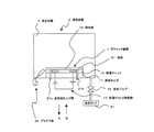
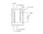
まず、図1および図2を参照して、第1の実施形態に係るデチャック機構1を有する真空装置2の概略構成を説明する。 First, a schematic configuration of a vacuum apparatus 2 having a dechuck mechanism 1 according to the first embodiment will be described with reference to FIGS. 1 and 2.
ここでは、真空装置2として、半導体の製造に用いられる真空装置が図示されている。 Here, a vacuum device used for manufacturing a semiconductor is shown as the vacuum device 2.
図1および図2に示すように、真空装置2は、チャンバとしての真空容器3を有している。 As shown in FIGS. 1 and 2, the vacuum device 2 has a vacuum container 3 as a chamber.
真空容器3の内部には基板ホルダ11が設けられており、基板ホルダ11には、静電吸引力によって基板51を保持する静電チャック15が設けられている。 A substrate holder 11 is provided inside the vacuum vessel 3, and the substrate holder 11 is provided with an electrostatic chuck 15 that holds the substrate 51 by electrostatic attraction force.
静電チャック15には、静電チャック15の動作用の静電チャック用電源17が接続されている。 An electrostatic chuck power source 17 for operating the electrostatic chuck 15 is connected to the electrostatic chuck 15.
また、静電チャック15は表面に基板51を保持する保持面16を有し、保持面16上には、プラズマ処理される基板51が保持される。 The electrostatic chuck 15 has a holding surface 16 for holding the substrate 51 on the surface, and the substrate 51 to be plasma-treated is held on the holding surface 16.
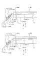
さらに、静電チャック15にはデチャックの際に静電チャック15から基板51を引き剥がすための基板突き上げ棒21a、21bが設けられている。
Further, the electrostatic chuck 15 is provided with substrate push-up
基板突き上げ棒21a、21bは図示しないアクチュエータによって図1のA、Bの向きに移動可能に設けられている。
The substrate push-up
例えば、図2(a)の状態から基板突き上げ棒21a、21bをBの向きに移動すると、基板51は基板突き上げ棒21a、21bに突き上げられ、図2(b)に示すように、静電チャック15から引き剥がされる。
For example, when the substrate push-up
また、真空容器3の内部にはさらに後述するプラズマ81を照射するプラズマ源23がデチャック用部品として設けられている。 Further, a plasma source 23 for irradiating a plasma 81 described later is provided as a dechucking component inside the vacuum vessel 3.
そして、静電チャック15、基板突き上げ棒21a、21b、プラズマ源23でデチャック機構1を構成している。
The electrostatic chuck 15, the substrate push-up
一方、真空容器3には、真空容器3内を排気するための真空ポンプ31が設けられている。真空ポンプ31と真空容器3の間には真空バルブ33が設けられている。
On the other hand, the vacuum vessel 3 is provided with a
次に、プラズマ源23の構造について、図2を参照して説明する。 Next, the structure of the plasma source 23 will be described with reference to FIG.
図2に示すように、プラズマ源23は、プラズマ81を発生させる中空のプラズマ発生容器37を有している。 As shown in FIG. 2, the plasma source 23 has a hollow plasma generation container 37 that generates plasma 81.
プラズマ発生容器37の一端は発生したプラズマ81を照射するプラズマ照射口39として開放されており、プラズマ照射口39は、保持面16と基板51の間を向くように設けられている。 One end of the plasma generation container 37 is opened as a plasma irradiation port 39 for irradiating the generated plasma 81, and the plasma irradiation port 39 is provided so as to face between the holding surface 16 and the substrate 51.
プラズマ発生容器37には、プラズマ化させるキャリアガスが流入するキャリアガス流入口41がさらに設けられている。 The plasma generation container 37 is further provided with a carrier gas inlet 41 into which a carrier gas to be converted into plasma flows.
キャリアガス流入口41は、図示しないキャリアガス源に接続されている。 The carrier gas inlet 41 is connected to a carrier gas source (not shown).
一方、プラズマ発生容器37内には、キャリアガスをプラズマ化してプラズマ81を発生させるためのフィラメント43が設けられており、フィラメント43は直流の電源45に接続されている。
On the other hand, a filament 43 for generating a plasma 81 by converting the carrier gas into plasma is provided in the plasma generation container 37, and the filament 43 is connected to a
なお、フィラメント43を構成する材料は例えばMo、Ta、Wである。 In addition, the material which comprises the filament 43 is Mo, Ta, and W, for example.
なお、前述のようにプラズマ照射口39は、保持面16と基板51の間を向くように設けられているが、プラズマ源23に図示しないアクチュエータを設け、プラズマ発生容器37(プラズマ照射口39)の向きを調整可能な構造としてもよい。 As described above, the plasma irradiation port 39 is provided so as to face between the holding surface 16 and the substrate 51. However, the plasma source 23 is provided with an actuator (not shown), and the plasma generation container 37 (plasma irradiation port 39) is provided. It is good also as a structure which can adjust direction of.
プラズマ源23からプラズマ81を発生させる場合は、プラズマ発生容器37内に、キャリアガス流入口41からAr、He、N2、空気等のキャリアガスを流入し、電源45を用いてフィラメント43に電流を流す。
When the plasma 81 is generated from the plasma source 23, a carrier gas such as Ar, He, N 2 , air, or the like flows into the plasma generation container 37 from the carrier gas inlet 41, and a current is supplied to the filament 43 using the
すると、フィラメント43は赤熱して熱電子を発生させる。 Then, the filament 43 is red hot and generates thermoelectrons.
発生した熱電子は、キャリアガスをプラズマ化させ、プラズマ81を発生させる。 The generated thermoelectrons turn the carrier gas into plasma and generate plasma 81.
発生したプラズマ81は、プラズマ照射口39より、保持面16と基板51の間に向けて照射される。 The generated plasma 81 is irradiated between the holding surface 16 and the substrate 51 from the plasma irradiation port 39.
次に、デチャック機構1を用いたデチャックの手順について図1および図2を用いて説明する。 Next, the procedure of dechucking using the dechuck mechanism 1 will be described with reference to FIGS.
まず、静電チャック用電源17を用いて、基板51が静電チャック15によってチャックされた状態であるとする。 First, it is assumed that the substrate 51 is chucked by the electrostatic chuck 15 using the electrostatic chuck power source 17.
まず、静電チャック用電源17をOFFにする。 First, the electrostatic chuck power supply 17 is turned off.
この状態では、保持面16と基板51には残留電荷が存在している。 In this state, residual charges exist on the holding surface 16 and the substrate 51.
次に、プラズマ源23を用いてプラズマ81を発生させる。なお、電源出力は例えば数10W程度である。 Next, plasma 81 is generated using the plasma source 23. For example, the power output is about several tens of watts.
発生したプラズマ81は、プラズマ照射口39より、保持面16と基板51の間に向けて照射される。 The generated plasma 81 is irradiated between the holding surface 16 and the substrate 51 from the plasma irradiation port 39.
次に、基板突き上げ棒21a、21bを図2(a)のBの向きに移動させ、基板51を静電チャック15から若干引き剥がす。
Next, the substrate push-up
すると、図2(b)に示すように、プラズマ照射口39から照射されたプラズマ81は、保持面16と基板51の間に入り込むため、保持面16と基板51の残留電荷は、プラズマ81により中和され、デチャックが迅速に進行する。 Then, as shown in FIG. 2B, since the plasma 81 irradiated from the plasma irradiation port 39 enters between the holding surface 16 and the substrate 51, the residual charges on the holding surface 16 and the substrate 51 are caused by the plasma 81. Neutralized and dechucking proceeds quickly.
そして、残留電荷が完全に中和されると、基板51は静電チャック15から完全に引き剥がされ、デチャックは終了する。 When the residual charge is completely neutralized, the substrate 51 is completely peeled off from the electrostatic chuck 15 and the dechuck is completed.
なお、デチャックに必要な時間は、基板の大きさにもよるが、数秒程度である。 The time required for dechucking is about several seconds although it depends on the size of the substrate.
このように、第1の実施形態によれば、デチャック機構1が静電チャック15およびプラズマ源23を有し、デチャックの際には、プラズマ源23から照射されたプラズマ81が、静電チャック15の保持面16と基板51の間に入り込んで残留電荷を中和することによりデチャックされる。 As described above, according to the first embodiment, the dechucking mechanism 1 has the electrostatic chuck 15 and the plasma source 23, and when dechucking, the plasma 81 irradiated from the plasma source 23 is changed to the electrostatic chuck 15. Is dechucked by entering between the holding surface 16 and the substrate 51 and neutralizing the residual charge.
従って、デチャック機構1は、静電チャック15や真空装置2の特性によらず、従来のデチャック機構よりもデチャック時間を短縮可能である。 Therefore, the dechucking mechanism 1 can shorten the dechucking time compared with the conventional dechucking mechanism regardless of the characteristics of the electrostatic chuck 15 and the vacuum device 2.
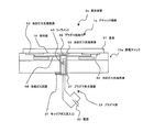
次に、第2の実施形態に係るデチャック機構1aを有する真空装置2aについて、図3を参照して、説明する。 Next, a vacuum apparatus 2a having a dechuck mechanism 1a according to the second embodiment will be described with reference to FIG.
なお、第2の実施形態において、第1の実施形態と同様の機能を果たす要素については同一の番号を付し、説明を省略する。 In the second embodiment, elements having the same functions as those in the first embodiment are denoted by the same reference numerals and description thereof is omitted.
第2の実施形態に係るデチャック機構1aを有する真空装置2aは、第1の実施形態において、静電チャック15の表面に冷却ガス充填用溝53を設け、冷却ガス充填用溝53に接するようにプラズマ源23を設けたものである。 The vacuum apparatus 2 a having the dechuck mechanism 1 a according to the second embodiment is provided with a cooling gas filling groove 53 on the surface of the electrostatic chuck 15 and in contact with the cooling gas filling groove 53 in the first embodiment. A plasma source 23 is provided.
なお、図3において、デチャック機構1a以外の真空装置2aの構造は第1の実施形態と同様であるため、記載を省略している。 In FIG. 3, the structure of the vacuum device 2 a other than the dechuck mechanism 1 a is the same as that in the first embodiment, and thus the description is omitted.
図3に示すように、デチャック機構1aは、静電チャック15aの保持面16に、He、N2等の冷却ガスを流すための冷却ガス充填用溝53が設けられている。 As shown in FIG. 3, the dechuck mechanism 1a is provided with a cooling gas filling groove 53 for flowing a cooling gas such as He or N 2 on the holding surface 16 of the electrostatic chuck 15a.
冷却ガス充填用溝53には、冷却ガスを冷却ガス充填用溝53に導入する冷却ガス流路55が接続されている。 A cooling gas passage 55 for introducing the cooling gas into the cooling gas filling groove 53 is connected to the cooling gas filling groove 53.
冷却ガス流路55は、静電チャック15a内に設けられており、一端が図示しない冷却ガス源に接続されている。 The cooling gas channel 55 is provided in the electrostatic chuck 15a, and one end thereof is connected to a cooling gas source (not shown).
また、静電チャック15aの内部には、冷却ガス充填用溝53に接するようにして、プラズマ源23が設けられている。 A plasma source 23 is provided inside the electrostatic chuck 15a so as to be in contact with the cooling gas filling groove 53.
プラズマ源23は、プラズマ照射口39が冷却ガス充填用溝53に接するように設けられている。 The plasma source 23 is provided such that the plasma irradiation port 39 is in contact with the cooling gas filling groove 53.
このように、静電チャック15aが冷却ガスを使用する構造の場合は、プラズマ源23を静電チャック15aの内部に設けてもよく、このような構造にすることにより、デチャック機構1aのサイズがコンパクトになる。 As described above, when the electrostatic chuck 15a has a structure using a cooling gas, the plasma source 23 may be provided inside the electrostatic chuck 15a. With this structure, the size of the dechuck mechanism 1a is reduced. It becomes compact.
また、保持面16に冷却ガス充填用溝53が設けられているため、基板突き上げ棒21a、21bは不要である。
Further, since the cooling gas filling groove 53 is provided on the holding surface 16, the substrate push-up
ここで、デチャック機構1aを用いたデチャックの手順について簡単に説明する。 Here, the procedure of dechucking using the dechucking mechanism 1a will be briefly described.
まず、基板51が静電チャック15aによってチャックされた状態であるとする。 First, it is assumed that the substrate 51 is in a state of being chucked by the electrostatic chuck 15a.
まず、静電チャック用電源17をOFFにする。 First, the electrostatic chuck power supply 17 is turned off.
次に、プラズマ源23を用いてプラズマ81を発生させる。 Next, plasma 81 is generated using the plasma source 23.
発生したプラズマ81は、プラズマ照射口39より、冷却ガス充填用溝53を介して保持面16と基板51の間に向けて照射され、保持面16と基板51の間に入り込む。 The generated plasma 81 is irradiated between the holding surface 16 and the substrate 51 from the plasma irradiation port 39 via the cooling gas filling groove 53 and enters between the holding surface 16 and the substrate 51.
すると、保持面16と基板51の残留電荷は、プラズマ81により中和され、デチャックが迅速に進行する。 Then, the residual charges on the holding surface 16 and the substrate 51 are neutralized by the plasma 81, and the dechucking proceeds rapidly.
そして、残留電荷が完全に中和されると、デチャックは終了する。 When the residual charge is completely neutralized, the dechuck is finished.
このように、第2の実施形態によれば、デチャック機構1aが静電チャック15aおよびプラズマ源23を有し、デチャックの際には、プラズマ源23から照射されたプラズマ81が、静電チャック15aの保持面16と基板51の間に入り込んで残留電荷を中和することによりデチャックされる。 As described above, according to the second embodiment, the dechuck mechanism 1a includes the electrostatic chuck 15a and the plasma source 23. When dechucking, the plasma 81 irradiated from the plasma source 23 is converted into the electrostatic chuck 15a. Is dechucked by entering between the holding surface 16 and the substrate 51 and neutralizing the residual charge.
従って、第1の実施形態と同様の効果を奏する。 Accordingly, the same effects as those of the first embodiment are obtained.
また、第2の実施形態によれば、プラズマ源23が静電チャック15aの内部に設けられている。 According to the second embodiment, the plasma source 23 is provided inside the electrostatic chuck 15a.
従って、第1の実施形態と比べてデチャック機構1aのサイズがコンパクトになる。 Therefore, the size of the dechuck mechanism 1a is compact compared to the first embodiment.
さらに、第2の実施形態によれば、保持面16に冷却ガス充填用溝53が設けられているため、基板突き上げ棒21a、21bは不要となる。
Furthermore, according to the second embodiment, since the cooling gas filling groove 53 is provided on the holding surface 16, the substrate push-up
次に、第3の実施形態に係るデチャック機構1bを有する真空装置2bについて、図4を参照して説明する。 Next, a vacuum apparatus 2b having a dechuck mechanism 1b according to a third embodiment will be described with reference to FIG.
なお、第3の実施形態において、第1の実施形態と同様の機能を果たす要素については同一の番号を付し、説明を省略する。 Note that in the third embodiment, elements that perform the same functions as those in the first embodiment are denoted by the same reference numerals, and description thereof is omitted.
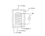
第3の実施形態に係るデチャック機構1bを有する真空装置2bは、第1の実施形態において、プラズマ源23bを、プラズマ発生用コイル63を有する構造としたものである。
The vacuum apparatus 2b having the dechuck mechanism 1b according to the third embodiment has a structure in which the plasma source 23b has a
なお、図4において、プラズマ源23b以外の真空装置2bの構造は第1の実施形態と同様であるため、記載を省略している。 In FIG. 4, since the structure of the vacuum apparatus 2b other than the plasma source 23b is the same as that of the first embodiment, the description is omitted.
図4に示すように、プラズマ源23bは、両端が開放された管状のプラズマ発生管61をプラズマ発生容器として有しており、プラズマ発生管61の一端をキャリアガス流入口61aとして用い、他端をプラズマ照射口61bとして用いている。 As shown in FIG. 4, the plasma source 23b has a tubular plasma generating tube 61 with both ends open as a plasma generating container, and one end of the plasma generating tube 61 is used as a carrier gas inlet 61a. Is used as the plasma irradiation port 61b.
また、プラズマ発生管61の周囲にはプラズマ発生用コイル63が設けられ、プラズマ発生用コイル63には交流の電源65が接続されている。
A
プラズマ源23bからプラズマ81を発生させる場合は、プラズマ発生管61にキャリアガス流入口61aからキャリアガスを流入し、電源65を用いてプラズマ発生用コイル63に電流を流す。
When the plasma 81 is generated from the plasma source 23 b, the carrier gas flows into the plasma generation tube 61 from the carrier gas inlet 61 a, and a current flows through the
すると、プラズマ発生用コイル63は誘導電流を発生させ、キャリアガスをプラズマ化させる。
Then, the
発生したプラズマ81は、プラズマ照射口61bより、保持面16と基板51の間に向けて照射される。 The generated plasma 81 is irradiated between the holding surface 16 and the substrate 51 from the plasma irradiation port 61b.
このように、プラズマ源23bを、プラズマ発生用コイル63を有する構造としてもよい。
As described above, the plasma source 23b may have a structure including the
このように、第3の実施形態によれば、デチャック機構1bが静電チャック15およびプラズマ源23bを有し、デチャックの際には、プラズマ源23bから照射されたプラズマ81が、静電チャック15の保持面16と基板51の間に入り込んで残留電荷を中和することによりデチャックされる。 As described above, according to the third embodiment, the dechuck mechanism 1b includes the electrostatic chuck 15 and the plasma source 23b, and during the dechucking, the plasma 81 irradiated from the plasma source 23b is converted into the electrostatic chuck 15. Is dechucked by entering between the holding surface 16 and the substrate 51 and neutralizing the residual charge.
従って、第1の実施形態と同様の効果を奏する。 Accordingly, the same effects as those of the first embodiment are obtained.
次に、第4の実施形態に係るデチャック機構1cを有する真空装置2cについて、図5を参照して説明する。 Next, a vacuum apparatus 2c having a dechuck mechanism 1c according to a fourth embodiment will be described with reference to FIG.
なお、第4の実施形態において、第3の実施形態と同様の機能を果たす要素については同一の番号を付し、説明を省略する。 Note that in the fourth embodiment, elements that perform the same functions as in the third embodiment are denoted by the same reference numerals, and descriptions thereof are omitted.
第4の実施形態に係るデチャック機構1cを有する真空装置2cは、第3の実施形態において、プラズマ発生用コイル69をプラズマ発生管67の内部に設けたものである。 A vacuum apparatus 2 c having a dechuck mechanism 1 c according to the fourth embodiment is such that a plasma generating coil 69 is provided inside a plasma generating tube 67 in the third embodiment.
なお、図5において、プラズマ源23c以外の真空装置2cの構造は第3の実施形態と同様であるため、記載を省略している。 In FIG. 5, the structure of the vacuum apparatus 2 c other than the plasma source 23 c is the same as that of the third embodiment, and thus the description is omitted.
図5に示すように、プラズマ源23cは、プラズマ発生管67をプラズマ発生容器として有しており、プラズマ発生管67の一端がキャリアガス流入口67aとして開放されており、他端がプラズマ照射口67bとして開放されている。 As shown in FIG. 5, the plasma source 23c has a plasma generation tube 67 as a plasma generation container, one end of the plasma generation tube 67 is opened as a carrier gas inlet 67a, and the other end is a plasma irradiation port. It is opened as 67b.
また、プラズマ発生管67の内部にはプラズマ発生用コイル69が設けられ、プラズマ発生用コイル69には交流の電源71が接続されている。 Further, a plasma generating coil 69 is provided inside the plasma generating tube 67, and an AC power supply 71 is connected to the plasma generating coil 69.
プラズマ源23cからプラズマ81を発生させる場合は、プラズマ発生管67にキャリアガス流入口67aからキャリアガスを流入し、電源71を用いてプラズマ発生用コイル69に電流を流す。 When the plasma 81 is generated from the plasma source 23 c, the carrier gas flows into the plasma generation tube 67 from the carrier gas inlet 67 a, and a current flows through the plasma generation coil 69 using the power source 71.
すると、プラズマ発生用コイル69は誘導電流を発生させ、キャリアガスをプラズマ化させる。 Then, the plasma generating coil 69 generates an induced current to turn the carrier gas into plasma.
発生したプラズマ81は、プラズマ照射口67bより、保持面16と基板51の間に向けて照射される。 The generated plasma 81 is irradiated between the holding surface 16 and the substrate 51 from the plasma irradiation port 67b.
このように、プラズマ発生用コイル69をプラズマ発生管67の内部に設けてもよい。 As described above, the plasma generating coil 69 may be provided inside the plasma generating tube 67.
このように、第4の実施形態によれば、デチャック機構1cが静電チャック15およびプラズマ源23cを有し、デチャックの際には、プラズマ源23cから照射されたプラズマ81が、静電チャック15の保持面16と基板51の間に入り込んで残留電荷を中和することによりデチャックされる。 As described above, according to the fourth embodiment, the dechuck mechanism 1c includes the electrostatic chuck 15 and the plasma source 23c, and the plasma 81 irradiated from the plasma source 23c is generated during the dechucking. Is dechucked by entering between the holding surface 16 and the substrate 51 and neutralizing the residual charge.
従って、第1の実施形態と同様の効果を奏する。 Accordingly, the same effects as those of the first embodiment are obtained.
次に、第5の実施形態に係るデチャック機構1dを有する真空装置2dについて、図6を参照して説明する。 Next, a vacuum apparatus 2d having a dechuck mechanism 1d according to a fifth embodiment will be described with reference to FIG.
なお、第5の実施形態において、第1の実施形態と同様の機能を果たす要素については同一の番号を付し、説明を省略する。 Note that in the fifth embodiment, elements that perform the same functions as in the first embodiment are denoted by the same reference numerals, and descriptions thereof are omitted.
第5の実施形態に係るデチャック機構1dを有する真空装置2dは、第1の実施形態において、プラズマ源23dを、電極75、77を有する構造としたものである。
A vacuum apparatus 2d having a dechuck mechanism 1d according to the fifth embodiment has a structure in which the plasma source 23d has
なお、図6において、プラズマ源23d以外の真空装置2dの構造は第1の実施形態と同様であるため、記載を省略している。 In FIG. 6, the structure of the vacuum apparatus 2 d other than the plasma source 23 d is the same as that of the first embodiment, and thus the description is omitted.
図6に示すように、プラズマ源23dは、プラズマ発生管73をプラズマ発生容器として有しており、プラズマ発生管73の一端がキャリアガス流入口73aとして開放されており、他端がプラズマ照射口73bとして開放されている。 As shown in FIG. 6, the plasma source 23d has a plasma generation tube 73 as a plasma generation container, one end of the plasma generation tube 73 is opened as a carrier gas inlet 73a, and the other end is a plasma irradiation port. 73b is opened.
また、プラズマ発生管73の内部には電極75、77が一対の電極として設けられ、電極75、77には交流の電源もしくはパルス電源である電源79が接続されている。
In addition,
プラズマ源23dからプラズマ81を発生させる場合は、プラズマ発生管73にキャリアガス流入口73aからキャリアガスを流入し、電源79を用いて電極75、77に電位を負荷する。
When the plasma 81 is generated from the plasma source 23d, a carrier gas is introduced into the plasma generation tube 73 from the carrier gas inlet 73a, and a potential is applied to the
すると、電極75、77間に放電が起こり、キャリアガスをプラズマ化させる。
Then, discharge occurs between the
発生したプラズマ81は、プラズマ照射口73bより、保持面16と基板51の間に向けて照射される。 The generated plasma 81 is irradiated between the holding surface 16 and the substrate 51 from the plasma irradiation port 73b.
このように、電極75、77を用いてプラズマ81を発生させてもよい。
Thus, the plasma 81 may be generated using the
このように、第5の実施形態によれば、デチャック機構1dが静電チャック15およびプラズマ源23dを有し、デチャックの際には、プラズマ源23dから照射されたプラズマ81が、静電チャック15の保持面16と基板51の間に入り込んで残留電荷を中和することによりデチャックされる。 Thus, according to the fifth embodiment, the dechucking mechanism 1d has the electrostatic chuck 15 and the plasma source 23d, and during the dechucking, the plasma 81 irradiated from the plasma source 23d is transformed into the electrostatic chuck 15. Is dechucked by entering between the holding surface 16 and the substrate 51 and neutralizing the residual charge.
従って、第1の実施形態と同様の効果を奏する。 Accordingly, the same effects as those of the first embodiment are obtained.
上記した実施形態では、本発明を半導体の製造に用いられる真空装置に適用した場合について説明したが、本発明は、何等、これに限定されることなく、静電チャックを必要とする全ての装置に用いることができる。 In the above-described embodiment, the case where the present invention is applied to a vacuum apparatus used for manufacturing a semiconductor has been described. However, the present invention is not limited to this, and all apparatuses that require an electrostatic chuck. Can be used.
例えば、本実施形態ではプラズマ源を別途設けているが、もともとプラズマ源のある真空装置の場合はそれを利用しても良い。 For example, although a plasma source is separately provided in this embodiment, it may be used in the case of a vacuum apparatus that originally has a plasma source.
この条件によれば、真空装置内のプラズマ維持の関係上、300〜500W程度の出力(13.56MHz)にて1〜2秒で電荷が抜けてデチャックが可能である。 According to this condition, due to the maintenance of plasma in the vacuum apparatus, dechucking is possible by removing the charge in 1 to 2 seconds at an output (13.56 MHz) of about 300 to 500 W.
1…………デチャック機構
2…………真空装置
3…………真空容器
11………基板ホルダ
15………静電チャック
17………静電チャック用電源
21a……基板突き上げ棒
23………プラズマ源
31………真空ポンプ
33………真空バルブ
37………プラズマ発生容器
39………プラズマ照射口
41………キャリアガス流入口
43………フィラメント
45………電源
53………冷却ガス充填用溝
55………冷却ガス流路
61………プラズマ発生管
61a……キャリアガス流入口
61b……プラズマ照射口
63………プラズマ発生用コイル
65………電源
67………プラズマ発生管
67a……キャリアガス流入口
67b……プラズマ照射口
69………プラズマ発生用コイル
71………電源
73………プラズマ発生管
73a……キャリアガス流入口
73b……プラズマ照射口
75………電極
77………電極
79………電源
1 ………… Dechucking mechanism 2 ………… Vacuum device 3 ………… Vacuum container 11 ……… Substrate holder 15 ……… Electrostatic chuck 17 ……… Electrostatic
Claims (14)
前記保持面と前記基板の間にプラズマを照射するプラズマ源と、
を有することを特徴とするデチャック機構。 An electrostatic chuck having a holding surface for holding a substrate;
A plasma source for irradiating plasma between the holding surface and the substrate;
A dechuck mechanism characterized by comprising:
前記プラズマ源は、前記冷却ガス充填用溝に接するように前記静電チャック内部に設けられていることを特徴とする請求項1記載のデチャック機構。 The holding surface is provided with a cooling gas filling groove,
The dechucking mechanism according to claim 1, wherein the plasma source is provided inside the electrostatic chuck so as to be in contact with the cooling gas filling groove.
プラズマ発生容器と、
前記プラズマ発生容器に設けられ、プラズマ化させるガスが流入するキャリアガス流入口と、
前記プラズマ発生容器に設けられ、プラズマを照射するプラズマ照射口と、
を有し、
前記プラズマ照射口は、前記保持面と前記基板の間を向くように設けられていることを特徴とする請求項1記載のデチャック機構。 The plasma source is:
A plasma generation container;
A carrier gas inlet provided in the plasma generation vessel and into which gas to be converted into plasma flows;
A plasma irradiation port that is provided in the plasma generation container and irradiates plasma;
Have
The dechucking mechanism according to claim 1, wherein the plasma irradiation port is provided so as to face between the holding surface and the substrate.
前記プラズマ発生容器内に設けられたフィラメントと、
前記フィラメントに接続された直流電源と、
を有することを特徴とする請求項4記載のデチャック機構。 The plasma source is:
A filament provided in the plasma generation vessel;
A direct current power source connected to the filament;
The dechuck mechanism according to claim 4, comprising:
前記プラズマ発生容器の周囲または内部に設けられたプラズマ発生用コイルと、
前記プラズマ発生用コイルに接続された交流電源と、
を有することを特徴とする請求項4記載のデチャック機構。 The plasma source is:
A plasma generating coil provided around or inside the plasma generating vessel;
An AC power source connected to the plasma generating coil;
The dechuck mechanism according to claim 4, comprising:
前記プラズマ発生容器内に設けられた一対の電極と、
一対の前記電極に接続された交流電源またはパルス電源と、
を有することを特徴とする請求項4記載のデチャック機構。 The plasma source is:
A pair of electrodes provided in the plasma generation container;
An AC power source or a pulse power source connected to the pair of electrodes;
The dechuck mechanism according to claim 4, comprising:
前記静電チャックの保持面と、前記保持面に保持された基板の間にプラズマを照射する工程を有することを特徴とするデチャック方法。 A dechucking method for dechucking a substrate held by an electrostatic chuck,
A dechucking method comprising irradiating plasma between a holding surface of the electrostatic chuck and a substrate held on the holding surface.
プラズマ発生容器と、
前記プラズマ発生容器に設けられ、プラズマ化させるガスが流入するキャリアガス流入口と、
前記プラズマ発生容器に設けられ、プラズマを照射するプラズマ照射口と、
を有し、
前記プラズマ照射口は、前記保持面と前記基板の間を向くように設けられていることを特徴とするデチャック用部品。 A dechucking component used for dechucking an electrostatic chuck having a holding surface for holding a substrate,
A plasma generation container;
A carrier gas inlet provided in the plasma generation vessel and into which gas to be converted into plasma flows;
A plasma irradiation port that is provided in the plasma generation container and irradiates plasma;
Have
The dechucking component, wherein the plasma irradiation port is provided so as to face between the holding surface and the substrate.
前記フィラメントに接続された直流電源と、
を有することを特徴とする請求項11記載のデチャック用部品。 A filament provided in the plasma generation vessel;
A direct current power source connected to the filament;
The dechucking component according to claim 11, comprising:
前記プラズマ発生容器の周囲または内部に設けられたプラズマ発生用コイルと、
前記プラズマ発生用コイルに接続された交流電源と、
を有することを特徴とする請求項11記載のデチャック用部品。 The plasma source is:
A plasma generating coil provided around or inside the plasma generating vessel;
An AC power source connected to the plasma generating coil;
The dechucking component according to claim 11, comprising:
前記プラズマ発生容器内に設けられた一対の電極と、
一対の前記電極に接続された交流電源またはパルス電源と、
を有することを特徴とする請求項11記載のデチャック用部品。 The plasma source is:
A pair of electrodes provided in the plasma generation container;
An AC power source or a pulse power source connected to the pair of electrodes;
The dechucking component according to claim 11, comprising:
Priority Applications (1)
| Application Number | Priority Date | Filing Date | Title |
|---|---|---|---|
| JP2008169163A JP5174553B2 (en) | 2008-06-27 | 2008-06-27 | Dechucking mechanism, vacuum device, dechucking method |
Applications Claiming Priority (1)
| Application Number | Priority Date | Filing Date | Title |
|---|---|---|---|
| JP2008169163A JP5174553B2 (en) | 2008-06-27 | 2008-06-27 | Dechucking mechanism, vacuum device, dechucking method |
Publications (2)
| Publication Number | Publication Date |
|---|---|
| JP2010010477A true JP2010010477A (en) | 2010-01-14 |
| JP5174553B2 JP5174553B2 (en) | 2013-04-03 |
Family
ID=41590596
Family Applications (1)
| Application Number | Title | Priority Date | Filing Date |
|---|---|---|---|
| JP2008169163A Expired - Fee Related JP5174553B2 (en) | 2008-06-27 | 2008-06-27 | Dechucking mechanism, vacuum device, dechucking method |
Country Status (1)
| Country | Link |
|---|---|
| JP (1) | JP5174553B2 (en) |
Cited By (4)
| Publication number | Priority date | Publication date | Assignee | Title |
|---|---|---|---|---|
| JP2014522103A (en) * | 2011-07-19 | 2014-08-28 | ラム リサーチ コーポレーション | Electrostatic chuck with plasma-assisted dechuck on wafer backside |
| KR20180108470A (en) | 2017-03-24 | 2018-10-04 | 스미도모쥬기가이 이온 테크놀로지 가부시키가이샤 | Wafer holding device and wafer detachment method |
| US10312061B2 (en) * | 2014-05-14 | 2019-06-04 | Boe Technology Group Co., Ltd. | Vacuum apparatus for vacuum treating substrate |
| WO2019197128A3 (en) * | 2018-04-12 | 2019-11-21 | Asml Netherlands B.V. | Apparatus comprising an electrostatic clamp and method for operating the apparatus |
Citations (7)
| Publication number | Priority date | Publication date | Assignee | Title |
|---|---|---|---|---|
| JPH11350140A (en) * | 1998-06-05 | 1999-12-21 | Mitsubishi Heavy Ind Ltd | Device for forming thin film of carbon nitride and its method |
| JP2002313902A (en) * | 2001-04-18 | 2002-10-25 | Canon Inc | Electrostatic chuck and method of dismounting substrate therefrom |
| JP2003282691A (en) * | 2002-03-26 | 2003-10-03 | Nec Kyushu Ltd | Electrostatic chuck for holding wafer and wafer separating method |
| JP2004047511A (en) * | 2002-07-08 | 2004-02-12 | Tokyo Electron Ltd | Method for releasing, method for processing, electrostatic attracting device, and treatment apparatus |
| JP2004231864A (en) * | 2003-01-31 | 2004-08-19 | National Institute Of Advanced Industrial & Technology | Method for surface-treatment of polymer film, surface-treating apparatus, polymer film treated by the treating method and polymer composite film |
| JP2006326553A (en) * | 2005-05-30 | 2006-12-07 | Taiyo Nippon Sanso Corp | Apparatus for treating exhaust gas |
| JP2007331953A (en) * | 2006-06-12 | 2007-12-27 | Tohoku Univ | Atom-involved silicon cluster and its producing method |
-
2008
- 2008-06-27 JP JP2008169163A patent/JP5174553B2/en not_active Expired - Fee Related
Patent Citations (7)
| Publication number | Priority date | Publication date | Assignee | Title |
|---|---|---|---|---|
| JPH11350140A (en) * | 1998-06-05 | 1999-12-21 | Mitsubishi Heavy Ind Ltd | Device for forming thin film of carbon nitride and its method |
| JP2002313902A (en) * | 2001-04-18 | 2002-10-25 | Canon Inc | Electrostatic chuck and method of dismounting substrate therefrom |
| JP2003282691A (en) * | 2002-03-26 | 2003-10-03 | Nec Kyushu Ltd | Electrostatic chuck for holding wafer and wafer separating method |
| JP2004047511A (en) * | 2002-07-08 | 2004-02-12 | Tokyo Electron Ltd | Method for releasing, method for processing, electrostatic attracting device, and treatment apparatus |
| JP2004231864A (en) * | 2003-01-31 | 2004-08-19 | National Institute Of Advanced Industrial & Technology | Method for surface-treatment of polymer film, surface-treating apparatus, polymer film treated by the treating method and polymer composite film |
| JP2006326553A (en) * | 2005-05-30 | 2006-12-07 | Taiyo Nippon Sanso Corp | Apparatus for treating exhaust gas |
| JP2007331953A (en) * | 2006-06-12 | 2007-12-27 | Tohoku Univ | Atom-involved silicon cluster and its producing method |
Cited By (5)
| Publication number | Priority date | Publication date | Assignee | Title |
|---|---|---|---|---|
| JP2014522103A (en) * | 2011-07-19 | 2014-08-28 | ラム リサーチ コーポレーション | Electrostatic chuck with plasma-assisted dechuck on wafer backside |
| KR101919644B1 (en) * | 2011-07-19 | 2019-02-08 | 램 리써치 코포레이션 | Electrostatic chuck with wafer backside plasma assisted dechuck |
| US10312061B2 (en) * | 2014-05-14 | 2019-06-04 | Boe Technology Group Co., Ltd. | Vacuum apparatus for vacuum treating substrate |
| KR20180108470A (en) | 2017-03-24 | 2018-10-04 | 스미도모쥬기가이 이온 테크놀로지 가부시키가이샤 | Wafer holding device and wafer detachment method |
| WO2019197128A3 (en) * | 2018-04-12 | 2019-11-21 | Asml Netherlands B.V. | Apparatus comprising an electrostatic clamp and method for operating the apparatus |
Also Published As
| Publication number | Publication date |
|---|---|
| JP5174553B2 (en) | 2013-04-03 |
Similar Documents
| Publication | Publication Date | Title |
|---|---|---|
| JP5479723B2 (en) | Plasma light source and plasma light generation method | |
| JP2009010263A (en) | Substrate bonding device | |
| JP4820359B2 (en) | Plasma processing equipment | |
| JP5174553B2 (en) | Dechucking mechanism, vacuum device, dechucking method | |
| JP2007134689A (en) | Substrate processing method and its device | |
| NL1033983A1 (en) | Device for generating extreme ultraviolet radiation by means of electrical discharge on regenerable electrodes. | |
| CN108431930A (en) | Atomic layer etch system with remote plasma source and DC electrodes | |
| JP6234271B2 (en) | Method for processing an object | |
| KR20200115273A (en) | Atomic layer etch(ale) of tungsten or other matal layers | |
| JP5317509B2 (en) | Plasma processing apparatus and method | |
| JP2006269556A (en) | Plasma processing apparatus and method of manufacturing semiconductor device | |
| JP4889562B2 (en) | Joining apparatus and joining method | |
| JP4936276B2 (en) | Nitriding equipment | |
| TW201724164A (en) | Plasma processing device and cleaning method thereof including a step for cleaning parts in a processing chamber and a step for cleaning a surface of a lifting push pin | |
| KR20110006932A (en) | Apparatus for fixing substrate | |
| JP2007234297A (en) | Plasma treatment device for tube | |
| JP2009194194A (en) | Method of plasma treatment | |
| JP5649153B2 (en) | Plasma processing apparatus and plasma processing method | |
| JP2005101617A (en) | Wafer bonding device and method thereof | |
| JP2020077657A (en) | Plasma processing apparatus and plasma processing method | |
| JP6204881B2 (en) | Method for processing an object | |
| JP2003124198A5 (en) | ||
| JP6142305B2 (en) | Electrostatic adsorption method and electrostatic adsorption device | |
| JP2007258097A (en) | Plasma processing apparatus | |
| JP2009262172A (en) | Electron beam irradiation device for reforming surface in through-hole |
Legal Events
| Date | Code | Title | Description |
|---|---|---|---|
| A621 | Written request for application examination |
Free format text: JAPANESE INTERMEDIATE CODE: A621 Effective date: 20100809 |
|
| A977 | Report on retrieval |
Free format text: JAPANESE INTERMEDIATE CODE: A971007 Effective date: 20110722 |
|
| A131 | Notification of reasons for refusal |
Free format text: JAPANESE INTERMEDIATE CODE: A131 Effective date: 20110803 |
|
| A521 | Request for written amendment filed |
Free format text: JAPANESE INTERMEDIATE CODE: A523 Effective date: 20110927 |
|
| A131 | Notification of reasons for refusal |
Free format text: JAPANESE INTERMEDIATE CODE: A131 Effective date: 20111019 |
|
| A521 | Request for written amendment filed |
Free format text: JAPANESE INTERMEDIATE CODE: A523 Effective date: 20111214 |
|
| A131 | Notification of reasons for refusal |
Free format text: JAPANESE INTERMEDIATE CODE: A131 Effective date: 20120418 |
|
| A521 | Request for written amendment filed |
Free format text: JAPANESE INTERMEDIATE CODE: A523 Effective date: 20120615 |
|
| TRDD | Decision of grant or rejection written | ||
| A01 | Written decision to grant a patent or to grant a registration (utility model) |
Free format text: JAPANESE INTERMEDIATE CODE: A01 Effective date: 20121205 |
|
| A61 | First payment of annual fees (during grant procedure) |
Free format text: JAPANESE INTERMEDIATE CODE: A61 Effective date: 20121228 |
|
| R150 | Certificate of patent or registration of utility model |
Ref document number: 5174553 Country of ref document: JP Free format text: JAPANESE INTERMEDIATE CODE: R150 |
|
| LAPS | Cancellation because of no payment of annual fees |