JP2010010168A - Integrated circuit device and electronic apparatus - Google Patents
Integrated circuit device and electronic apparatus Download PDFInfo
- Publication number
- JP2010010168A JP2010010168A JP2008164129A JP2008164129A JP2010010168A JP 2010010168 A JP2010010168 A JP 2010010168A JP 2008164129 A JP2008164129 A JP 2008164129A JP 2008164129 A JP2008164129 A JP 2008164129A JP 2010010168 A JP2010010168 A JP 2010010168A
- Authority
- JP
- Japan
- Prior art keywords
- oscillation
- oscillation circuit
- substrate
- region
- integrated circuit
- Prior art date
- Legal status (The legal status is an assumption and is not a legal conclusion. Google has not performed a legal analysis and makes no representation as to the accuracy of the status listed.)
- Granted
Links
Images


Classifications
-
- H—ELECTRICITY
- H01—ELECTRIC ELEMENTS
- H01L—SEMICONDUCTOR DEVICES NOT COVERED BY CLASS H10
- H01L24/00—Arrangements for connecting or disconnecting semiconductor or solid-state bodies; Methods or apparatus related thereto
- H01L24/01—Means for bonding being attached to, or being formed on, the surface to be connected, e.g. chip-to-package, die-attach, "first-level" interconnects; Manufacturing methods related thereto
- H01L24/02—Bonding areas ; Manufacturing methods related thereto
- H01L24/04—Structure, shape, material or disposition of the bonding areas prior to the connecting process
- H01L24/06—Structure, shape, material or disposition of the bonding areas prior to the connecting process of a plurality of bonding areas
-
- H—ELECTRICITY
- H01—ELECTRIC ELEMENTS
- H01L—SEMICONDUCTOR DEVICES NOT COVERED BY CLASS H10
- H01L2224/00—Indexing scheme for arrangements for connecting or disconnecting semiconductor or solid-state bodies and methods related thereto as covered by H01L24/00
- H01L2224/01—Means for bonding being attached to, or being formed on, the surface to be connected, e.g. chip-to-package, die-attach, "first-level" interconnects; Manufacturing methods related thereto
- H01L2224/02—Bonding areas; Manufacturing methods related thereto
- H01L2224/04—Structure, shape, material or disposition of the bonding areas prior to the connecting process
- H01L2224/05—Structure, shape, material or disposition of the bonding areas prior to the connecting process of an individual bonding area
- H01L2224/0554—External layer
- H01L2224/0555—Shape
- H01L2224/05552—Shape in top view
- H01L2224/05554—Shape in top view being square
-
- H—ELECTRICITY
- H01—ELECTRIC ELEMENTS
- H01L—SEMICONDUCTOR DEVICES NOT COVERED BY CLASS H10
- H01L2224/00—Indexing scheme for arrangements for connecting or disconnecting semiconductor or solid-state bodies and methods related thereto as covered by H01L24/00
- H01L2224/01—Means for bonding being attached to, or being formed on, the surface to be connected, e.g. chip-to-package, die-attach, "first-level" interconnects; Manufacturing methods related thereto
- H01L2224/42—Wire connectors; Manufacturing methods related thereto
- H01L2224/47—Structure, shape, material or disposition of the wire connectors after the connecting process
- H01L2224/48—Structure, shape, material or disposition of the wire connectors after the connecting process of an individual wire connector
- H01L2224/4805—Shape
- H01L2224/4809—Loop shape
- H01L2224/48091—Arched
-
- H—ELECTRICITY
- H01—ELECTRIC ELEMENTS
- H01L—SEMICONDUCTOR DEVICES NOT COVERED BY CLASS H10
- H01L2224/00—Indexing scheme for arrangements for connecting or disconnecting semiconductor or solid-state bodies and methods related thereto as covered by H01L24/00
- H01L2224/01—Means for bonding being attached to, or being formed on, the surface to be connected, e.g. chip-to-package, die-attach, "first-level" interconnects; Manufacturing methods related thereto
- H01L2224/42—Wire connectors; Manufacturing methods related thereto
- H01L2224/47—Structure, shape, material or disposition of the wire connectors after the connecting process
- H01L2224/49—Structure, shape, material or disposition of the wire connectors after the connecting process of a plurality of wire connectors
- H01L2224/491—Disposition
- H01L2224/4912—Layout
- H01L2224/49175—Parallel arrangements
-
- H—ELECTRICITY
- H01—ELECTRIC ELEMENTS
- H01L—SEMICONDUCTOR DEVICES NOT COVERED BY CLASS H10
- H01L2924/00—Indexing scheme for arrangements or methods for connecting or disconnecting semiconductor or solid-state bodies as covered by H01L24/00
- H01L2924/10—Details of semiconductor or other solid state devices to be connected
- H01L2924/11—Device type
- H01L2924/14—Integrated circuits
-
- H—ELECTRICITY
- H01—ELECTRIC ELEMENTS
- H01L—SEMICONDUCTOR DEVICES NOT COVERED BY CLASS H10
- H01L2924/00—Indexing scheme for arrangements or methods for connecting or disconnecting semiconductor or solid-state bodies as covered by H01L24/00
- H01L2924/30—Technical effects
- H01L2924/301—Electrical effects
- H01L2924/3011—Impedance
Abstract
Description
本発明は、集積回路装置及び電子機器に関する。 The present invention relates to an integrated circuit device and an electronic apparatus.
近年、時計や携帯電話等の携帯機器(広義には電子機器)では、より一層の小型化や低コスト化が求められている。そのため、携帯機器に搭載される半導体集積回路装置(広義には集積回路装置)が実装されるシステム基板上において、信号の配線領域の増大を抑えることが行われている(例えば特許文献1を参照)。或いは、携帯機器に搭載される半導体集積回路装置(広義には集積回路装置)に、例えば中央演算処理装置(Central Processing Unit:CPU)、メモリ、タイマ、発振回路等の周辺回路を内蔵させることが行われている。 In recent years, further downsizing and cost reduction have been demanded for portable devices such as watches and mobile phones (electronic devices in a broad sense). Therefore, an increase in signal wiring area is suppressed on a system board on which a semiconductor integrated circuit device (an integrated circuit device in a broad sense) mounted on a portable device is mounted (see, for example, Patent Document 1). ). Alternatively, a semiconductor integrated circuit device (integrated circuit device in a broad sense) mounted on a portable device may incorporate peripheral circuits such as a central processing unit (CPU), a memory, a timer, and an oscillation circuit. Has been done.
特に、CPUや周辺回路等の動作クロックを生成する発振回路を半導体集積回路装置に内蔵させた場合、半導体集積回路装置内で動作クロックを各回路に分配できるため、低消費電力化の効果も得ることができる。 In particular, when an oscillation circuit for generating an operation clock such as a CPU or a peripheral circuit is built in a semiconductor integrated circuit device, the operation clock can be distributed to each circuit in the semiconductor integrated circuit device, so that an effect of reducing power consumption can be obtained. be able to.
ところで、発振回路を内蔵する半導体集積回路装置には、該発振回路の外付け部品として発振振動子等が接続される。また、発振回路は、ノイズの影響を受けやすい一方で、ノイズの発生源となることが多い。そのため、半導体基板(半導体チップ、チップ)において発振回路のマクロブロックの配置位置を考慮する必要がある。 By the way, to a semiconductor integrated circuit device incorporating an oscillation circuit, an oscillation vibrator or the like is connected as an external component of the oscillation circuit. In addition, the oscillation circuit is easily affected by noise, but often becomes a noise generation source. Therefore, it is necessary to consider the arrangement position of the macro block of the oscillation circuit on the semiconductor substrate (semiconductor chip, chip).
しかしながら、半導体基板のコーナー部には、該半導体基板を識別するための記号、製造時のマスク等の位置決めのための目印、又は製造精度を確認するためのモニター回路等が配置されるものの、コーナー部の未使用エリアが無駄に存在している。そのため、発振回路を半導体集積回路装置に内蔵させた場合であっても、この未使用エリアに起因して、半導体基板のサイズを小さくするにも限界があり、低コスト化の妨げとなる場合がある。 However, the corner portion of the semiconductor substrate is provided with a symbol for identifying the semiconductor substrate, a mark for positioning a mask at the time of manufacturing, or a monitor circuit for checking manufacturing accuracy. Some unused areas are in vain. Therefore, even when the oscillation circuit is built in the semiconductor integrated circuit device, there is a limit in reducing the size of the semiconductor substrate due to this unused area, which may hinder cost reduction. is there.
また、半導体集積回路装置に発振回路を内蔵させたとしても、該半導体集積回路装置が実装されるシステム基板上において、発振回路の外付け部品の配置が考慮されていない。そのため、システム基板上で信号線を避けるために発振信号が伝送される信号線の等長性を失わせてしまう。これを回避するために、システム基板を構成する基板層数を増加させる必要があり、コスト高を招く場合がある。 Even if an oscillation circuit is incorporated in the semiconductor integrated circuit device, the arrangement of external components of the oscillation circuit is not considered on the system board on which the semiconductor integrated circuit device is mounted. For this reason, in order to avoid the signal line on the system board, the equal length of the signal line through which the oscillation signal is transmitted is lost. In order to avoid this, it is necessary to increase the number of board layers constituting the system board, which may increase the cost.
更に、発振回路を内蔵する半導体集積回路装置では、発振回路へのノイズの影響等を考慮する必要がある。そのため、半導体集積回路装置において、ノイズの影響を低減する対策を講じたり、同じ半導体基板に配置されるその他の回路のマクロブロックの配置位置を決定するためフロアプランの大きな制約となったりして、コスト高を招く場合がある。 Furthermore, in a semiconductor integrated circuit device incorporating an oscillation circuit, it is necessary to consider the influence of noise on the oscillation circuit. Therefore, in the semiconductor integrated circuit device, taking measures to reduce the influence of noise, or to determine the placement position of the macroblocks of other circuits placed on the same semiconductor substrate, it becomes a major constraint of the floor plan, High costs may be incurred.
本発明は、以上のような技術的課題に鑑みてなされたものであり、その目的の1つは、発振回路を内蔵した場合であっても低コスト化を図ることができる集積回路装置及び電子機器を提供することにある。 The present invention has been made in view of the technical problems as described above, and one of the objects thereof is an integrated circuit device and an electronic device capable of reducing the cost even when an oscillation circuit is incorporated. To provide equipment.
上記課題を解決するために本発明は、基板と、前記基板の縁部に沿って設けられたI/O(Input/Output)セル領域に配置された複数のI/Oセルと、前記I/Oセル領域に配置され発振回路を有する発振回路ブロックとを含み、前記発振回路ブロックが、前記I/Oセル領域内において前記基板のコーナー領域を含む配置領域に配置される集積回路装置に関係する。 In order to solve the above problems, the present invention provides a substrate, a plurality of I / O cells arranged in an I / O (Input / Output) cell region provided along an edge of the substrate, and the I / O An oscillation circuit block having an oscillation circuit disposed in an O cell region, wherein the oscillation circuit block is related to an integrated circuit device disposed in an arrangement region including a corner region of the substrate in the I / O cell region .
また本発明に係る集積回路装置では、前記配置領域は、第1の方向に前記複数のI/Oセルのいずれかが一列に配列される領域と、該第1の方向と交差する第2の方向に前記複数のI/Oセルのいずれかが一列に配列される領域との交差領域を含む領域であってもよい。 In the integrated circuit device according to the present invention, the arrangement region includes a region in which any of the plurality of I / O cells is arranged in a row in a first direction, and a second region that intersects the first direction. It may be a region including an intersecting region with a region in which any of the plurality of I / O cells is arranged in a row in the direction.
上記のいずれかの発明によれば、基板の縁部に沿って設けられたI/Oセル領域内において該基板のコーナー領域を含む配置領域に発振回路ブロックを配置するようにしたので、無駄なエリアと考えられていた基板のコーナー領域を有効活用して、基板のサイズを縮小して、低コスト化を図ることができるようになる。また、上記のいずれかの発明によれば、発振回路がI/Oセルの影響を受けやすくなる場合であっても、電源分離や専用電源を用意してI/Oセルの影響を低コストで回避できるようになる。また、上記のいずれかの発明によれば、その近傍の周辺の外部端子の種類にかかわらず、ノイズの影響を受けることなく発振回路の発振動作を低コストで安定化させることができるようになる。更に、発振回路ブロックの近くにノイズ源となり得る信号線が配置されることを考慮する必要がなくなり、回路配線が容易となる。その結果、開発工数が削減されて、低コスト化に寄与できるようになる。更に、上記のいずれかの発明によれば、発振回路ブロックと内部領域に配置される他の回路ブロックとの配置距離を十分に取れるようになるので、基板内のフロアプランの制約が緩和されて設計効率が向上し、開発工数を削減できるようになる。 According to any one of the above-described inventions, the oscillation circuit block is arranged in the arrangement region including the corner region of the substrate in the I / O cell region provided along the edge of the substrate. By effectively utilizing the corner area of the substrate, which has been considered as an area, the size of the substrate can be reduced and the cost can be reduced. In addition, according to any one of the above-described inventions, even when the oscillation circuit is easily affected by the I / O cell, power supply separation or a dedicated power supply is prepared to reduce the influence of the I / O cell at a low cost. It can be avoided. In addition, according to any one of the above inventions, the oscillation operation of the oscillation circuit can be stabilized at a low cost without being affected by noise regardless of the types of peripheral external terminals in the vicinity thereof. . Furthermore, it is not necessary to consider that a signal line that can be a noise source is arranged near the oscillation circuit block, and the circuit wiring becomes easy. As a result, the number of development man-hours can be reduced, and the cost can be reduced. Furthermore, according to any one of the above-described inventions, the arrangement distance between the oscillation circuit block and the other circuit blocks arranged in the internal region can be sufficiently secured, so that the restrictions on the floor plan in the substrate are relaxed. Design efficiency is improved and development man-hours can be reduced.
また本発明は、基板と、前記基板の縁部に沿って設けられたI/O(Input/Output)セル領域に配置された複数のI/Oセルと、前記複数のI/Oセルを構成する各I/Oセルに接続され、該各I/Oセルに電源電圧を供給するための環状電源配線と、前記基板のコーナー領域に配置され発振回路を有する発振回路ブロックとを含み、前記発振回路ブロックが、前記コーナー領域内で前記環状電源配線の外側に設けられた配置領域に配置される集積回路装置に関係する。 The present invention also comprises a substrate, a plurality of I / O cells arranged in an I / O (Input / Output) cell region provided along an edge of the substrate, and the plurality of I / O cells. An oscillation circuit block connected to each I / O cell for supplying a power supply voltage to each I / O cell and an oscillation circuit block having an oscillation circuit disposed in a corner region of the substrate. The circuit block relates to an integrated circuit device arranged in an arrangement area provided outside the annular power supply wiring in the corner area.
本発明によれば、基板のコーナー領域のうちI/Oセルの環状電源配線の外側に発振回路ブロックを配置するようにしたので、発振振動子と接続される高インピーダンスラインである信号線とがクロスする必要がなくなり、発振回路の発振動作を低コストで安定化させることができるようになる。また、本発明によれば、基板においてコーナー領域内で環状電源配線の外側に設けられた配置領域に発振回路ブロックを配置するようにしたので、無駄なエリアと考えられていた基板のコーナー領域を有効活用して、基板のサイズを縮小して、低コスト化を図ることができるようになる。また、本発明によれば、発振回路がI/Oセルの影響を受けやすくなる場合であっても、電源分離や専用電源を用意してI/Oセルの影響を低コストで回避できるようになる。また、本発明によれば、その近傍の周辺の外部端子の種類にかかわらず、ノイズの影響を受けることなく発振回路の発振動作を低コストで安定化させることができるようになる。更に、発振回路ブロックの近くにノイズ源となり得る信号線が配置されることを考慮する必要がなくなり、回路配線が容易となる。その結果、開発工数が削減されて、低コスト化に寄与できるようになる。更に、本発明によれば、発振回路ブロックと内部領域に配置される他の回路ブロックとの配置距離を十分に取れるようになるので、基板内のフロアプランの制約が緩和されて設計効率が向上し、開発工数を削減できるようになる。 According to the present invention, since the oscillation circuit block is arranged outside the annular power supply wiring of the I / O cell in the corner region of the substrate, the signal line that is a high impedance line connected to the oscillation vibrator is There is no need to cross, and the oscillation operation of the oscillation circuit can be stabilized at a low cost. Further, according to the present invention, since the oscillation circuit block is arranged in the arrangement area provided outside the annular power supply wiring in the corner area of the board, the corner area of the board that is considered as a useless area Effective use makes it possible to reduce the size of the substrate and reduce the cost. Further, according to the present invention, even when the oscillation circuit is susceptible to the influence of the I / O cell, the influence of the I / O cell can be avoided at a low cost by preparing power source separation and a dedicated power source. Become. Furthermore, according to the present invention, the oscillation operation of the oscillation circuit can be stabilized at a low cost without being affected by noise regardless of the types of peripheral external terminals in the vicinity thereof. Furthermore, it is not necessary to consider that a signal line that can be a noise source is arranged near the oscillation circuit block, and the circuit wiring becomes easy. As a result, the number of development man-hours can be reduced, and the cost can be reduced. Furthermore, according to the present invention, a sufficient arrangement distance between the oscillation circuit block and other circuit blocks arranged in the internal region can be secured, so that the restrictions on the floor plan in the board are relaxed and the design efficiency is improved. And development man-hours can be reduced.
また本発明に係る集積回路装置では、前記基板に配置され、前記発振回路と発振振動子の一端とを電気的に接続するための第1の外部端子と、前記基板に配置され、前記発振回路と前記発振振動子の他端とを電気的に接続するための第2の外部端子とを含み、前記第1及び第2の外部端子が、前記配置領域に配置されてもよい。 Further, in the integrated circuit device according to the present invention, the oscillation circuit is disposed on the substrate, and is disposed on the substrate and a first external terminal for electrically connecting the oscillation circuit and one end of the oscillation vibrator. And a second external terminal for electrically connecting the other end of the oscillation vibrator, and the first and second external terminals may be arranged in the arrangement region.
本発明によれば、基板の外部において、発振回路に極力近い位置に発振振動子を配置しやすくなる上に、発振信号が伝送される信号線を他の信号線と無駄にクロスさせずに済み、低コストで信頼性を向上させることができる。また、本発明によれば、発振振動子とのマッチングのために容量素子や抵抗素子を外部で更に付加する必要がある場合でも、これらの素子を配置できる位置を容易に確保できるため、低コストで使い勝手を向上させることができるようになる。 According to the present invention, it is easy to dispose the oscillation vibrator as close as possible to the oscillation circuit outside the substrate, and the signal line for transmitting the oscillation signal does not need to be crossed with other signal lines. Reliability can be improved at low cost. In addition, according to the present invention, even when it is necessary to add a capacitance element or a resistance element externally for matching with the oscillation vibrator, a position where these elements can be arranged can be easily secured, so that the cost can be reduced. Can improve usability.
また本発明は、基板と、前記基板に配置され発振回路を有する発振回路ブロックと、前記基板に配置され、前記発振回路と発振振動子の一端とを電気的に接続するための第1の外部端子と、前記基板に配置され、前記発振回路と前記発振振動子の他端とを電気的に接続するための第2の外部端子とを含み、前記発振回路ブロック、前記第1及び第2の外部端子が、前記基板のコーナー領域に設けられた配置領域に配置される集積回路装置に関係する。 The present invention also provides a first external circuit for electrically connecting a substrate, an oscillation circuit block disposed on the substrate and having an oscillation circuit, and the oscillation circuit and one end of the oscillation vibrator disposed on the substrate. A terminal and a second external terminal disposed on the substrate for electrically connecting the oscillation circuit and the other end of the oscillation vibrator, the oscillation circuit block, the first and second The external terminal relates to an integrated circuit device arranged in an arrangement area provided in a corner area of the substrate.
本発明によれば、基板のコーナー領域に発振回路ブロックを配置するようにしたので、無駄なエリアと考えられていた基板のコーナー領域を有効活用して、基板のサイズを縮小して、低コスト化を図ることができるようになる。また、本発明によれば、発振回路がI/Oセルの影響を受けやすくなる場合であっても、電源分離や専用電源を用意してI/Oセルの影響を低コストで回避できるようになる。また、本発明によれば、その近傍の周辺の外部端子の種類にかかわらず、ノイズの影響を受けることなく発振回路の発振動作を低コストで安定化させることができるようになる。更に、発振回路ブロックの近くにノイズ源となり得る信号線が配置されることを考慮する必要がなくなり、回路配線が容易となる。その結果、開発工数が削減されて、低コスト化に寄与できるようになる。更に、本発明によれば、発振回路ブロックと内部領域に配置される他の回路ブロックとの配置距離を十分に取れるようになるので、基板内のフロアプランの制約が緩和されて設計効率が向上し、開発工数を削減できるようになる。 According to the present invention, since the oscillation circuit block is arranged in the corner area of the substrate, the corner area of the substrate, which has been considered a useless area, can be effectively used to reduce the size of the substrate and reduce the cost. It becomes possible to plan. Further, according to the present invention, even when the oscillation circuit is susceptible to the influence of the I / O cell, the influence of the I / O cell can be avoided at a low cost by preparing power source separation and a dedicated power source. Become. Furthermore, according to the present invention, the oscillation operation of the oscillation circuit can be stabilized at a low cost without being affected by noise regardless of the types of peripheral external terminals in the vicinity thereof. Furthermore, it is not necessary to consider that a signal line that can be a noise source is arranged near the oscillation circuit block, and the circuit wiring becomes easy. As a result, the number of development man-hours can be reduced, and the cost can be reduced. Furthermore, according to the present invention, a sufficient arrangement distance between the oscillation circuit block and other circuit blocks arranged in the internal region can be secured, so that the restrictions on the floor plan in the board are relaxed and the design efficiency is improved. And development man-hours can be reduced.
また本発明に係る集積回路装置では、前記発振回路の電源電圧を制御する定電圧発生回路を含み、前記定電圧発生回路が、前記配置領域に配置されてもよい。 The integrated circuit device according to the present invention may further include a constant voltage generation circuit that controls a power supply voltage of the oscillation circuit, and the constant voltage generation circuit may be arranged in the arrangement region.
また本発明に係る集積回路装置では、前記基板に配置され、前記発振回路及び前記定電圧発生回路の低電位側電源が供給される第3の外部端子と、前記基板に配置され、前記定電圧発生回路の高電位側電源が供給される第4の外部端子とを含み、前記第3及び第4の外部端子が、前記配置領域に配置されてもよい。 In the integrated circuit device according to the present invention, a third external terminal disposed on the substrate and supplied with a low-potential-side power source of the oscillation circuit and the constant voltage generation circuit, disposed on the substrate, and the constant voltage And a fourth external terminal to which a high-potential-side power supply of the generation circuit is supplied, and the third and fourth external terminals may be arranged in the arrangement region.
本発明によれば、発振回路に関連する信号線と他の信号線と無駄にクロスさせずに済み、低コストで信頼性を向上させることができる。 According to the present invention, it is not necessary to wastefully cross a signal line related to the oscillation circuit and another signal line, and reliability can be improved at low cost.
また本発明に係る集積回路装置では、少なくとも前記発振回路ブロックの周囲に、所与の固定電圧が印加される領域が設けられてもよい。 In the integrated circuit device according to the present invention, a region to which a given fixed voltage is applied may be provided at least around the oscillation circuit block.
本発明によれば、近くに配置されるI/Oセルの影響を確実に抑え、低コストで発振回路の発振動作を安定化させることができる。 According to the present invention, it is possible to reliably suppress the influence of an I / O cell disposed nearby and stabilize the oscillation operation of the oscillation circuit at low cost.
また本発明に係る集積回路装置では、前記発振回路を構成する素子が、前記基板に設けられた第1の不純物領域内に形成され、前記複数のI/Oセルの各I/Oセルを構成する素子が、前記基板に設けられた第2の不純物領域内に形成される場合に、前記第1及び第2の不純物領域が分離されていてもよい。 In the integrated circuit device according to the present invention, the elements constituting the oscillation circuit are formed in a first impurity region provided in the substrate, and each I / O cell of the plurality of I / O cells is configured. When the element to be formed is formed in the second impurity region provided in the substrate, the first and second impurity regions may be separated.
本発明によれば、近くに配置されるI/Oセルの影響を確実に抑え、低コストで発振回路の発振動作を安定化させることができる。 According to the present invention, it is possible to reliably suppress the influence of an I / O cell disposed nearby and stabilize the oscillation operation of the oscillation circuit at low cost.
また本発明に係る集積回路装置では、前記基板に配置され、前記発振回路の電源端子に安定化用キャパシタを電気的に接続するための第5の外部端子を含み、前記第5の外部端子が、前記配置領域に配置されてもよい。 In the integrated circuit device according to the present invention, the integrated circuit device includes a fifth external terminal that is disposed on the substrate and electrically connects a stabilization capacitor to a power supply terminal of the oscillation circuit. , May be arranged in the arrangement area.
本発明によれば、発振回路の発振動作を安定化する際に、発振回路に関連する信号線と他の信号線と無駄にクロスさせずに済み、低コストで信頼性を向上させることができる。 According to the present invention, when stabilizing the oscillation operation of the oscillation circuit, it is not necessary to cross the signal line related to the oscillation circuit and other signal lines unnecessarily, and the reliability can be improved at low cost. .
また本発明に係る集積回路装置では、前記基板に配置され、発振振動子からの入力信号が入力される第1の発振回路専用I/Oセルと、前記基板に配置され、前記発振振動子への出力信号を出力する第2の発振回路専用I/Oセルとを含み、前記第1及び第2の発振回路専用I/Oセルが、前記複数のI/Oセルのいずれともその構成が異なり、前記発振回路専用に設けられたI/Oセルであってもよい。 In the integrated circuit device according to the present invention, the first oscillation circuit-dedicated I / O cell, which is arranged on the substrate and receives an input signal from the oscillation vibrator, is arranged on the substrate, and is connected to the oscillation vibrator. A second oscillation circuit dedicated I / O cell that outputs the output signal of the first oscillation circuit, and the first and second oscillation circuit dedicated I / O cells differ in configuration from any of the plurality of I / O cells. The I / O cell may be provided exclusively for the oscillation circuit.
本発明によれば、発振回路専用のI/Oセルを設けることで、信号経路の抵抗値や容量値を考慮した設計変更が不要となり、特性を揃えた状態で他の集積回路装置に流用できるようになる。しかも、発振回路専用のI/Oセルを周囲のI/Oセルに合わせ無駄に大きくする必要がなくなり、基板のサイズを小さくできるようになる。 According to the present invention, by providing the dedicated I / O cell for the oscillation circuit, it is not necessary to change the design in consideration of the resistance value and capacitance value of the signal path, and it can be used for other integrated circuit devices in a state where the characteristics are uniform. It becomes like this. In addition, it is not necessary to wastefully increase the size of the I / O cell dedicated to the oscillation circuit in accordance with the surrounding I / O cells, and the size of the substrate can be reduced.
また本発明は、システム基板と、前記システム基板上に搭載される上記のいずれか記載の集積回路装置と、前記システム基板上に搭載され前記発振回路に電気的に接続される発振振動子とを含む電子機器に関係する。 According to another aspect of the present invention, there is provided a system board, the integrated circuit device according to any one of the above described mounted on the system board, and an oscillation vibrator mounted on the system board and electrically connected to the oscillation circuit. Related to electronic equipment.
本発明によれば、発振回路を内蔵した場合であっても低コスト化を図ることができる集積回路装置を含む電子機器を提供できるようになる。 According to the present invention, it is possible to provide an electronic apparatus including an integrated circuit device capable of reducing the cost even when an oscillation circuit is incorporated.
また本発明に係る電子機器では、前記発振振動子が、前記集積回路装置のコーナー部の近傍領域に配置されてもよい。 In the electronic apparatus according to the present invention, the oscillation vibrator may be arranged in a region near a corner portion of the integrated circuit device.
本発明によれば、集積回路装置のコーナー部を有効活用して、発振回路の発振動作をより一層安定化させると共に、電子機器の小型化を図ることができるようになる。 According to the present invention, the corner portion of the integrated circuit device can be effectively used to further stabilize the oscillation operation of the oscillation circuit and to reduce the size of the electronic device.
以下、本発明の実施の形態について図面を用いて詳細に説明する。なお、以下に説明する実施の形態は、特許請求の範囲に記載された本発明の内容を不当に限定するものではない。また以下で説明される構成のすべてが本発明の必須構成要件であるとは限らない。 Hereinafter, embodiments of the present invention will be described in detail with reference to the drawings. The embodiments described below do not unduly limit the contents of the present invention described in the claims. Also, not all of the configurations described below are essential constituent requirements of the present invention.
以下では、本発明に係る集積回路装置として、発振回路の他にCPUやLCD(Liquid Crystal Display)パネルの駆動回路を含む集積回路装置を例に説明するが、本発明に係る集積回路装置はCPUやLCDパネルの駆動回路を含むものに限定されるものではない。 Hereinafter, as an integrated circuit device according to the present invention, an integrated circuit device including a CPU and an LCD (Liquid Crystal Display) panel drive circuit in addition to an oscillation circuit will be described as an example. However, the integrated circuit device according to the present invention is a CPU. It is not limited to the one including the drive circuit for the LCD panel.
1.集積回路装置
〔実施形態1〕
図1に、本発明に係る実施形態1における集積回路装置の構成例の機能ブロック図を示す。
1. Integrated circuit device [Embodiment 1]
FIG. 1 shows a functional block diagram of a configuration example of an integrated circuit device according to the first embodiment of the present invention.
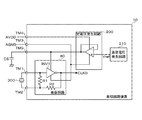
集積回路装置10は、発振回路80、CPU110、ROM(Read Only Memory)112、RAM(Random Access Memory)114、第1及び第2の周辺回路116、118、I/O(Input/Output)ポート120、表示メモリ122、LCD駆動回路124、電源回路126、及びバス130を含む。CPU110、ROM112、RAM114、第1及び第2の周辺回路116、118、I/Oポート120、表示メモリ122、LCD駆動回路124、及び電源回路126は、バス130を介し電気的に接続される。
The
この集積回路装置10は、外部端子群P1、P2、第1〜第5の外部端子TM1〜TM5を有する。外部端子群P1、P2は、それぞれ複数の端子により構成される。外部端子群P1、P2を構成する各端子や第1〜第5の外部端子TM1〜TM5を構成する各端子は、I/O(Input/Output)回路と電気的に接続され半導体基板(チップ)上に形成されたパッドを有する。各パッドとこれに対応するIC(Integrated Circuit)パッケージのピンとがボンディングワイヤを介して電気的に接続される。
The
CPU110は、ROM112又はRAM114に記憶されたプログラムをバス130を介して読み出し、該プログラムに対応した処理を実行することで、集積回路装置10の全体の制御を司る。
The
ROM112には、CPU110のプログラム又は各種の制御データが予め記憶されており、CPU110又は他の回路がバス130を介してROM112からプログラム又は制御データを読み出す。
The
RAM114には、CPU110、第1及び第2の周辺回路116、118、及びI/Oポート120のワークエリアとして、データが一時的に格納されたり、表示メモリ122に格納される表示データが一時的に格納されたりする。
The
第1の周辺回路116は、例えば割り込みコントローラ、タイマ回路やウオッチドッグタイマにより構成され、バス130を介してCPU110により設定された条件で動作し、その動作結果をCPU110に通知することができるようになっている。
The first
第2の周辺回路118は、例えばプログラマブルタイマやシリアルインターフェス回路により構成され、バス130を介してCPU110により設定された条件で動作し、I/Oポート120を経由して、外部端子群P2を介して信号が入力又は出力されるようになっている。
The second
I/Oポート120は、汎用ポートとして機能し、外部端子群P2を構成する端子のいずれかを介して信号の入力や出力が行われる。
The I /
表示メモリ122には、CPU110により生成された図示しないLCDパネルの1画面分の表示データが記憶される。表示メモリ122に記憶された表示データは、LCD駆動回路124に送られる。外部端子群P1には、LCDパネルのコモン電極やセグメント電極が電気的に接続される。LCD駆動回路124は、CPU110により設定された表示駆動条件で、外部端子群P1を介してLCDパネルを駆動する。
The
電源回路126は、集積回路装置10を構成する各回路ブロックの電源を生成する。この電源回路126は、バス130を介してCPU110により設定された条件で、各回路ブロックの電源電圧を生成する。
The
発振回路80には、集積回路装置10の外部において第1及び第2の外部端子TM1、TM2を介して発振振動子(或いは発振振動子及びキャパシタ)が接続される。発振回路80は、発振振動子からの発振信号に基づいて発振動作を行う。
An oscillation oscillator (or an oscillation oscillator and a capacitor) is connected to the
また、発振回路80には、第3及び第4の外部端子TM3、TM4を介して外部から電源が供給される。第3の外部端子TM3には、集積回路装置10の外部から所与のアナログ接地電圧が供給される。第4の外部端子TM4には、集積回路装置10の外部から所与のアナログ高電位側電圧が供給される。発振回路80又は後述する定電圧発生回路が、第3及び第4の外部端子TM3、TM4を介して供給された電圧に基づいて、安定した定電圧を生成し、該定電圧が供給された状態で上記の発振動作を行う。
The
更に、発振回路80には、集積回路装置10の外部において第5の外部端子TM5を介して、安定化用キャパシタCSが接続される。安定化用キャパシタCSにより、発振回路80の電源電圧の変動が小さくなる。
Further, the stabilization circuit CS is connected to the
このような発振回路80は、発振振動子からの発振信号に基づいて生成された基準クロックCLK0又は図示しない分周回路で基準クロックCLK0を分周した分周クロックを、集積回路装置10の各回路に動作クロックとして分配する。
Such an
図2に、実施形態1における発振回路80の構成例を示す。図2は、発振回路80と共に集積回路装置10に内蔵される各種回路ブロックをあわせて表す。図2において、図1と同一部分には同一符号を付し、適宜説明を省略する。
FIG. 2 shows a configuration example of the
集積回路装置10は、図1に示す発振回路80等の回路ブロックの他に、発振回路80の電源電圧を制御する定電圧発生回路200と、基準電圧発生回路210とを含むことができる。なお、発振回路80が、定電圧発生回路200の機能を含んでもよい。また、図1の電源回路126が、基準電圧発生回路210の機能を含んでもよい。
The
発振回路80は、インバータ回路INV1、抵抗素子R1、R2を含む。インバータ回路INV1の入力端子は、図示しないI/Oセルを介して、第1の外部端子TM1に電気的に接続される。発振回路80の内部において、第1及び第2の外部端子TM1、TM2の間に抵抗素子R1が挿入される。インバータ回路INV1の出力端子と第2の外部端子TM2に対応する図示しないI/Oセルとの間に抵抗素子R2が挿入され、インバータ回路INV1の出力端子から基準クロックCLK0が出力される。
The
インバータ回路INV1の高電位側電源電圧は、定電圧発生回路200により生成される。定電圧発生回路200は、所与の電源電圧AVDDと接地電圧AGNDが供給されるボルテージフォロア回路を有する。ボルテージフォロア回路の高電位側電源端子は、図示しないI/Oセルを介して、第4の外部端子TM4が電気的に接続される。ボルテージフォロア回路の低電位側電源端子及び発振回路80のインバータ回路INV1の低電位側電源端子は、図示しないI/Oセルを介して、第3の外部端子TM3が電気的に接続される。ボルテージフォロア回路の入力には、基準電圧発生回路210により生成された基準電圧Vrefが供給される。基準電圧発生回路210の機能は、バンドギャップリファレンス回路や、所与の電圧間に挿入された抵抗分割回路等により実現される。
The high potential side power supply voltage of the inverter circuit INV1 is generated by the constant
定電圧発生回路200のボルテージフォロア回路の出力は、図示しないI/Oセルを介して、第5の外部端子TM5に電気的に接続されると共に、発振回路80のインバータ回路INV1の高電位側電源電圧として供給される。第5の外部端子TM5には、集積回路装置10の外部において安定化用キャパシタCSの一端が接続され、安定化用キャパシタCSの他端には接地電圧AGNDが供給される。このような安定化用キャパシタCSを第5の外部端子TM5に接続することで、定電圧発生回路200が発生する定電圧が安定化し、発振回路80の発振動作を安定化させることができる。
The output of the voltage follower circuit of the constant
なお、発振回路80のインバータ回路の高電位側電源電圧が安定する場合には、集積回路装置10は第5の外部端子TM5を省略した構成を有し、外付け部品として安定化用キャパシタCSを省略してもよい。
When the high potential side power supply voltage of the inverter circuit of the
発振回路80は、上記のような定電圧発生回路200からの定電圧が供給された状態で、発振振動子300からの発振信号に基づいて発振動作を行い、所与の周波数の基準クロックCLK0を出力する。このような発振回路80は、発振振動子を水晶振動子とする水晶発振回路であってもよいし、発振振動子をセラミック振動子とするセラミック発振回路であってもよい。
The
図3に、実施形態1における集積回路装置10のフロアプランイメージを示す。図3は、集積回路装置10を構成する各回路ブロックが形成される半導体基板(広義には基板、チップ)の上面図であり、フロアプランイメージを模式的に表す。
FIG. 3 shows a floor plan image of the
図1及び図2に示す集積回路装置10の各回路ブロックが形成される半導体基板400は、平面視において矩形の形状を有している。そして、矩形の半導体基板400の縁部に沿ってI/Oセル領域(I/O回路領域)410が設けられる。この半導体基板400の縁部に沿って設けられる領域を、半導体基板400の外周部ということができる。
The
I/Oセル領域410では、外部端子群P1、P2、第1〜第5の外部端子TM1〜TM5の各外部端子に対応して設けられるI/Oセル(I/Oセル)が配置される。より具体的には、I/Oセル領域410では、半導体基板400の端部(縁部)に沿ってパッド404が配列され、各パッドに対応した長方形の形状を有するI/Oセル402の長辺方向が、該端部が延びる方向と交差するように配置される。
In the I /
図4に、実施形態1におけるI/Oセル402が有するI/O回路の構成例の回路図を示す。図4は、入力用の外部端子に対応するI/Oセルの構成例を表す。
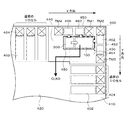
FIG. 4 is a circuit diagram showing a configuration example of the I / O circuit included in the I /
I/Oセル402は、外部端子としてのパッド404と接地電源線との間に挿入される静電保護素子としてのnpn型トランジスタTr1と、入力保護抵抗R3と、入力バッファとしてのインバータ回路INV2とを含む。npn型トランジスタTr1のベースには、エミッタと同じ接地電圧が供給され、npn型トランジスタTr1のコレクタには、パッド404が電気的に接続される。入力保護抵抗R3は、パッド404と、インバータ回路INV2の入力との間に挿入される。インバータ回路INV2の出力信号が、内部回路に出力される。
The I /
なお、図4では、入力用の外部端子に対応するI/Oセルの構成例を示したが、出力用の外部端子に対応するI/Oセルは、出力バッファ及び静電保護素子を有し、入出力用の外部端子に対応するI/Oセルは、入力バッファ、出力バッファ、入力保護抵抗及び静電保護素子を有する。 Note that FIG. 4 shows a configuration example of the I / O cell corresponding to the input external terminal, but the I / O cell corresponding to the output external terminal has an output buffer and an electrostatic protection element. The I / O cell corresponding to the input / output external terminal includes an input buffer, an output buffer, an input protection resistor, and an electrostatic protection element.
図3において、半導体基板400のコア領域420(周囲がI/Oセル領域410に囲まれる領域)には、図1及び図2に示す集積回路装置10の回路ブロックのうち発振回路ブロック100を除く回路ブロックが配置される。なお、図3では、コア領域420に配置される図1の各回路ブロックの図示を省略している。
3, in the core region 420 (region surrounded by the I / O cell region 410) of the
半導体基板400の4つのコーナー領域のいずれかのコーナー領域には、発振回路ブロック100が配置される。発振回路ブロック100は、発振回路80と少なくとも第1及び第2の外部端子TM1、TM2とを有する。このコーナー領域には、更に、第3〜第5の外部端子TM3〜TM5(第5の外部端子TM5が省略された場合には第3、第4の外部端子TM3、TM4)が配置されることが望ましい。発振回路ブロック100が、第3〜第5の外部端子TM1〜TM5を含んでもよい。発振回路ブロック100、第3〜第5の外部端子TM3〜TM5が配置されるコーナー領域は、I/Oセル領域410内に存在する。
The
より具体的には、I/Oセル領域410において、半導体基板400のコーナー領域を含む配置領域440に配置される。即ち、ここで、X方向(第1の方向)に複数のI/Oセル402のいずれかが一列に配列される第1のI/Oセル領域と、該X方向と直交(交差)するY方向(第2の方向)に複数のI/Oセル402の別のいずれかが一列に配列される第2のI/Oセル領域とを定義すると、発振回路ブロック100、及び第1〜第5の外部端子TM1〜TM5が、I/Oセル領域410のうち、第1及び第2のI/Oセル領域とが交差する交差領域430を含む配置領域440に配置される。なお、第5の外部端子TM5が省略された場合には第1〜第4の外部端子TM1〜TM4が配置領域440に配置される。
More specifically, in the I /
このように、これまで実質的に未使用エリアとして考えられていた半導体基板400のコーナー領域に発振回路ブロック100を配置するようにしたので、半導体基板400のサイズを小さくでき、低コスト化を図ることができるようになる。特に、実施形態1では、I/Oセル領域410のうち、コーナー領域又は交差領域430を含む配置領域440に、発振回路ブロック100を配置するようにしたので、I/Oセル領域が半導体基板の縁部に沿って設けられる場合に未使用エリアとなりやすい領域を有効活用でき、半導体基板400のサイズをより一層縮小できるようになる。
As described above, since the
図5に、図3の配置領域440の拡大図を模式的に示す。なお、図5において、第5の外部端子TM5が省略されている。図5において、図3と同一部分には同一符号を付し、適宜説明を省略する。
FIG. 5 schematically shows an enlarged view of the
図5に示すように、実施形態1では、I/Oセル領域410内において、X方向にI/Oセルが配列される領域とY方向にI/Oセルが配列される領域とが交差する交差領域430が設けられる。このとき、配置領域440は、I/Oセル領域410であって、半導体基板400のコーナー部に設けられた交差領域430含む領域となる。
As shown in FIG. 5, in the first embodiment, in the I /
更に、この配置領域440には、発振回路ブロック100の他に、定電圧発生回路200、第1〜第4の外部端子TM1〜TM4が配置されている。発振回路ブロック100は、定電圧発生回路200、第1〜第4の外部端子TM1〜TM4を含んでもよい。第1、第2及び第4の外部端子TM1、TM2、TM4は、半導体基板400のX方向に延びる端部450の縁部に沿って配置される。第2及び第3の外部端子TM2、TM3は、半導体基板400のY方向に延びる端部452の縁部に沿って配置される。
Further, in addition to the
また、実施形態1では、発振回路80及び定電圧発生回路200に入力又は出力される信号をインターフェースするI/Oセルは、配置領域440を除くI/Oセル領域410に配列されるI/Oセル402を流用するのではなく、発振回路専用に設けられたI/Oセルである。
In the first embodiment, the I / O cells that interface signals input or output to the
即ち、第1の外部端子TM1に対応して第1の発振回路専用I/Oセル460が設けられ、第1の発振回路専用I/Oセル460と第1の外部端子TM1(パッド)とが端部450に沿ってX方向に並んで配置される。第1の発振回路専用I/Oセル460は、発振振動子300からの入力信号が入力される。
That is, the first oscillation circuit dedicated I /
第2の外部端子TM2に対応して第2の発振回路専用I/Oセル462が設けられ、第2の外部端子TM2(パッド)と第2の発振回路専用I/Oセル462とが端部452に沿ってY方向に並んで配置される。第2の発振回路専用I/Oセル462は、発振振動子300への出力信号を出力する。
A second oscillation circuit dedicated I /
第3の外部端子TM3に対応して第3の発振回路専用I/Oセル464が設けられ、第3の発振回路専用I/Oセル464と第3の外部端子TM3(パッド)とが端部452に沿ってY方向に並んで配置される。
A third oscillation circuit dedicated I /
第4の外部端子TM4に対応して第4の発振回路専用I/Oセル466が設けられ、第4の外部端子TM4(パッド)と第4の発振回路専用I/Oセル466とが端部450に沿ってX方向に並んで配置される。
A fourth oscillation circuit dedicated I /
図6に、実施形態1における第1の発振回路専用I/Oセル460が有するI/O回路の構成例の回路図を示す。図6は、第1の発振回路専用I/Oセル460の構成例を表すが、第2〜第4の発振回路専用I/Oセル462〜466もまた、図6と同様の構成を有することができる。また、第5の外部端子TM5に対応して設けられる第5の発振回路専用I/Oセルもまた、図6と同様の構成を有することができる。
FIG. 6 is a circuit diagram showing a configuration example of the I / O circuit included in the first oscillation circuit dedicated I /
第1の発振回路専用I/Oセル460は、第1の外部端子TM1(パッド)と接地電源線との間に挿入される静電保護素子としてのnpn型トランジスタTr2と、入力保護抵抗R4とを含む。npn型トランジスタTr2のベースには、エミッタと同じ接地電圧が供給され、npn型トランジスタTr2のコレクタには、第1の外部端子TM1が電気的に接続される。入力保護抵抗R4は、第1の外部端子TM1と、発振回路80との間に挿入される。
The first oscillation circuit dedicated I /
第1の発振回路専用I/Oセル460では、npn型トランジスタTr2のサイズが静電気保護機能を実現する最小限のサイズで実現されている。そのため、第1の発振回路専用I/Oセル460は、I/Oセルの領域を小さくできる。これにより、第1の発振回路専用I/Oセル460は、入力バッファや出力バッファ等を有しI/Oセル領域410に配置されるその他の通常のI/Oセル402とは異なる構成を有している。
In the first oscillation circuit dedicated I /
このように、第1〜第5の発振回路専用I/Oセル(図5では、第1〜第4の発振回路専用I/Oセル)は、I/Oセル領域410に配置されるその他の通常のI/Oセル402のいずれともその構成が異なり、発振回路80専用に設けられたI/Oセルである。発振回路専用I/Oセルを設け、発振回路ブロック100と同じ配置領域440内に配置させることで、発振回路ブロック100及び発振回路用のI/Oセルをその都度設計する必要がなくなり、特性を揃えた状態で他の集積回路装置に流用できるようになる。この結果、開発工数を削減して、集積回路装置の低コスト化に寄与できるようになる。
As described above, the first to fifth oscillation circuit dedicated I / O cells (in FIG. 5, the first to fourth oscillation circuit dedicated I / O cells) are arranged in the I /
なお、半導体基板400において、少なくとも発振回路ブロック100の周囲に、例えば接地電源電圧等の固定電圧が印加される領域480が、発振回路ブロック100のガードリングとして設けられることが望ましい。より具体的には、半導体基板400において、発振回路80及び定電圧発生回路200の周囲に、例えば接地電源電圧等の固定電圧が印加される領域が、発振回路ブロック100のガードリングとして設けられることが望ましい。
In the
或いは、発振回路80(或いは発振回路80及び定電圧発生回路200)を構成するトランジスタ素子(広義には素子)が、半導体基板400に設けられた第1のウェル領域(第1の不純物領域)内に形成され、I/Oセル領域410内のI/Oセルを構成するトランジスタ素子が、半導体基板400に設けられた第2のウェル領域(第2の不純物領域)内に形成される場合に、第1及び第2のウェル領域が分離されていることが望ましい。これは、発振回路80(或いは発振回路80及び定電圧発生回路200)を、いわゆるトリプルウェル構造で形成することで実現される。
Alternatively, transistor elements (elements in a broad sense) constituting the oscillation circuit 80 (or the
こうすることで、発振回路80(発振回路ブロック100)にI/Oセル402の信号変動に伴うノイズの影響を及ぼさずに済むため、発振回路80の発振動作を安定化させることができる。
By doing so, the oscillation circuit 80 (oscillation circuit block 100) can be prevented from being affected by noise associated with signal fluctuations of the I /
〔実施形態2〕
実施形態1における集積回路装置10は、半導体基板400のコーナー領域における交差領域430を含む配置領域440に発振回路ブロック100を配置していたが、本発明はこれに限定されるものではない。実施形態2では、半導体基板のコーナー領域のうち、I/Oセル領域に配置されるI/Oセルに接続される環状電源配線の外側に設けられた配線領域に、発振回路ブロック100が配置される。
[Embodiment 2]
In the
本発明に係る実施形態2における集積回路装置500は、実施形態1における集積回路装置10と同様の回路ブロックを有するため、実施形態2における集積回路装置が有する回路ブロックについての説明を省略する。
Since the
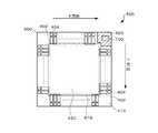
図7に、実施形態2における集積回路装置500のフロアプランイメージを示す。図7は、集積回路装置10を構成する各回路ブロックが形成される半導体基板の上面図であり、フロアプランイメージを模式的に表す。図7において、図3と同様の部分には同一番号を付し、適宜説明を省略する。
FIG. 7 shows a floor plan image of the
実施形態2における集積回路装置500の各回路ブロックが形成される半導体基板600は、平面視において矩形の形状を有している。そして、矩形の半導体基板600の縁部に沿ってI/Oセル領域410が設けられる。この半導体基板600の縁部に沿って設けられる領域を、半導体基板600の外周部ということができる。
The
I/Oセル領域410では、実施形態1と同様に、外部端子群P1、P2、第1〜第5の外部端子TM1〜TM5の各外部端子に対応して設けられるI/Oセル及びパッドが配置される。更に、I/Oセル領域410には、I/Oセル領域410内に配置された複数のI/Oセルを構成する各I/Oセルに接続され各I/Oセルに電源電圧を供給するための環状電源配線610が配置されている。そして、半導体基板600のコーナー領域内であって、環状電源配線610の外側に設けられた配置領域620に、発振回路ブロック100(発振回路80と少なくとも第1及び第2の外部端子TM1、TM2)が配置される。この配置領域620には、更に、第3〜第5の外部端子TM1〜TM5(第5の外部端子TM5が省略された場合には第3、第4の外部端子TM3、TM4)が配置されることが望ましい。
In the I /
このように、これまで実質的に未使用エリアが存在していた半導体基板600のコーナー領域であって、I/Oセルの環状電源配線610の外側に発振回路ブロック100を配置するようにしたので、発振動作に関連する信号線と環状電源配線610とのカップリング等を低減し、且つ半導体基板600のサイズを小さくして、低コスト化を図ることができるようになる。
As described above, the
図8に、図7の配置領域620の拡大図を模式的に示す。なお、図8において、第5の外部端子TM5が省略されている。図8において、図5又は図7と同一部分には同一符号を付し、適宜説明を省略する。また、図8では、環状電源配線610として、I/Oセル402の低電位側電源電圧を供給するための接地電圧環状電源配線612と、I/Oセル402の高電位側電源電圧を供給するための電源電圧環状電源配線614とが設けられている。
FIG. 8 schematically shows an enlarged view of the
図8に示すように、実施形態2では、I/Oセル領域410内において、接地電圧環状電源配線612及び電源電圧環状電源配線614からなる環状電源配線610の外側に設けられた配置領域620が設けられる。
As shown in FIG. 8, in the second embodiment, an
この配置領域620には、発振回路ブロック100の他に、定電圧発生回路200、第1〜第4の外部端子TM1〜TM4が配置されている。第1、第2及び第4の外部端子TM1、TM2、TM4は、半導体基板600のX方向に延びる端部650の縁部に沿って配置される。第2及び第3の外部端子TM2、TM3は、半導体基板600のY方向に延びる端部652の縁部に沿って配置される。なお、発振回路ブロック100に、定電圧発生回路200、第1〜第4の外部端子TM1〜TM4を含めてもよい。
In this
また、実施形態2では、実施形態1と同様に、発振回路80及び定電圧発生回路200に入力又は出力される信号をインターフェースするI/Oセルは、発振回路専用に設けられたI/Oセルである。
In the second embodiment, as in the first embodiment, an I / O cell that interfaces signals input or output to the
なお、実施形態2においても、半導体基板600において、少なくとも発振回路ブロック100の周囲に、例えば接地電源電圧等の固定電圧が印加される領域480が、発振回路ブロック100のガードリングとして設けられることが望ましい。より具体的には、半導体基板600において、発振回路80及び定電圧発生回路200の周囲に、例えば接地電源電圧等の固定電圧が印加される領域が、発振回路ブロック100のガードリングとして設けられることが望ましい。
In the second embodiment, a
或いは、発振回路80(或いは発振回路80及び定電圧発生回路200)を構成するトランジスタ素子が、半導体基板600に設けられた第1のウェル領域内に形成され、I/Oセル領域410内のI/Oセルを構成するトランジスタ素子が、半導体基板600に設けられた第2のウェル領域内に形成される場合に、第1及び第2のウェル領域が分離されていることが望ましい。
Alternatively, transistor elements constituting the oscillation circuit 80 (or the
こうすることで、発振回路80にI/Oセル402の信号変動に伴うノイズの影響を及ぼさずに済むため、発振回路80の発振動作を安定化させることができる。
By doing so, the
上記の実施形態1における集積回路装置10又は実施形態2における集積回路装置500によれば、例えば次のような効果を得ることができる。
According to the
図9に、本発明に係る集積回路装置の効果の説明図を示す。 FIG. 9 is an explanatory diagram of the effect of the integrated circuit device according to the present invention.
図9は、実施形態1における集積回路装置10の半導体基板400又は実施形態2における集積回路装置500の半導体基板600と、他の集積回路装置を構成する半導体基板700とがスタックされてなる半導体装置680を表す。半導体基板400又は半導体基板600のパッドは、半導体基板700又はこの半導体装置680の外部端子とボンディングワイヤ702を介して電気的に接続される。このとき、この半導体装置の内部又は外部に設けられる発振振動子と、半導体基板400又は半導体基板600に形成された発振回路ブロック100の発振回路80との間で信号線704を介して発振信号が入出力される。
FIG. 9 shows a semiconductor device in which the
上記のいずれかの実施形態によれば、発振回路ブロック100を半導体基板のコーナー領域に配置するようにしたので、信号線704が半導体基板の角部に接続される。そのため、半導体基板700とスタックさせる際に、基板の配置やボンディングワイヤの接続の邪魔にならず、スタックの際の半導体基板の実装の自由度を向上させることができるようになる。
According to any one of the above embodiments, since the
図10に、本発明に係る集積回路装置の効果の説明図を示す。 FIG. 10 is an explanatory diagram of the effect of the integrated circuit device according to the present invention.
図10は、実施形態1における集積回路装置10の半導体基板400又は実施形態2における集積回路装置500の半導体基板600が、リードフレームのダイパッドに搭載された半導体装置750を表す。この半導体装置750は、半導体基板400又は半導体基板600に形成された発振回路ブロック100の発振回路80と信号線を介して接続され、且つモールドエリア752に設けられた発振振動子300を含む。
FIG. 10 shows a
上記のいずれかの実施形態によれば、発振回路ブロック100を半導体基板のコーナー領域に配置するようにしたので、発振振動子300をモールドエリアの空きエリアに配置できるようになり、半導体装置750の集積度を向上させて低コスト化に寄与できるようになる。
According to any one of the above embodiments, since the
このように上記のいずれかの実施形態によれば、発振回路ブロック100(発振回路80)の端子位置がネックとなり困難と考えられてきた複数の半導体基板によるスタック構造や発振振動子のパッケージ内封入が可能となり、集積回路装置の活用度を向上させて低コスト化に寄与できるようになる。 As described above, according to any of the above-described embodiments, the terminal position of the oscillation circuit block 100 (oscillation circuit 80) is a bottleneck and has been considered to be a stack structure with a plurality of semiconductor substrates or the enclosure of the oscillation vibrator in the package. As a result, the utilization of the integrated circuit device can be improved and the cost can be reduced.
以上説明したように、上記のいずれかの実施形態によれば、無駄なエリアと考えられていた半導体基板のコーナー領域に発振回路等を配置するようにしたので、半導体基板のサイズを縮小して、低コスト化を図ることができるようになる。 As described above, according to any of the above embodiments, the oscillation circuit or the like is arranged in the corner region of the semiconductor substrate that was considered a useless area. This makes it possible to reduce costs.
また、上記のいずれかの実施形態によれば、半導体基板の外部において、発振回路に極力近い位置に発振振動子を配置しやすくなる上に、発振信号が伝送される信号線を他の信号線と無駄にクロスさせずに済み、低コストで信頼性を向上させることができる。 In addition, according to any one of the above embodiments, it is easy to arrange the oscillation vibrator at a position as close as possible to the oscillation circuit outside the semiconductor substrate, and the signal line through which the oscillation signal is transmitted is connected to the other signal line. Therefore, it is possible to improve the reliability at low cost.
また、上記のいずれかの実施形態によれば、発振振動子とのマッチングのために容量素子や抵抗素子を外部で更に付加する必要がある場合でも、これらの素子を配置できる位置を容易に確保できるため、低コストで使い勝手を向上させることができるようになる。 In addition, according to any of the above-described embodiments, even when it is necessary to add a capacitive element or a resistive element externally for matching with the oscillation vibrator, a position where these elements can be arranged is easily secured. Therefore, usability can be improved at low cost.
また、上記のいずれかの実施形態によれば、発振回路(発振回路ブロック)がI/Oセルの影響を受けやすくなる場合であっても、半導体基板のコーナー領域に発振回路ブロックを配置することで、電源分離や専用電源を用意してI/Oセルの影響を低コストで回避できるようになる。しかも、上記のいずれかの実施形態のように、不純物領域の分離やガードリングを施すことで、確実にI/Oセルの影響を抑えることが可能となる。 Further, according to any one of the above embodiments, the oscillation circuit block is arranged in the corner region of the semiconductor substrate even when the oscillation circuit (oscillation circuit block) is easily affected by the I / O cell. Thus, it is possible to avoid the influence of the I / O cell at low cost by preparing a power source separation or a dedicated power source. Moreover, as in any of the above-described embodiments, the influence of the I / O cell can be reliably suppressed by performing the separation of the impurity regions and the guard ring.
また、上記のいずれかの実施形態によれば、半導体基板のコーナー領域のうちI/Oセルの環状電源配線の外側に発振回路ブロックを配置することで、発振振動子と接続される高インピーダンスラインである信号線とがクロスする必要がなくなり、発振回路の発振動作を低コストで安定化させることができるようになる。 In addition, according to any one of the above embodiments, the high impedance line connected to the oscillation vibrator is provided by disposing the oscillation circuit block outside the annular power supply wiring of the I / O cell in the corner region of the semiconductor substrate. Therefore, it is not necessary to cross the signal line, and the oscillation operation of the oscillation circuit can be stabilized at a low cost.
また、上記のいずれかの実施形態によれば、半導体基板のコーナー領域に発振回路ブロックを配置することで、近傍の周辺の外部端子の種類にかかわらず、ノイズの影響を受けることなく発振回路の発振動作を低コストで安定化させることができるようになる。更に、発振回路ブロックの近くをノイズ源となり得る信号線の配置を考慮する必要がなくなり、回路配線が容易となる。その結果、開発工数が削減されて、低コスト化に寄与できるようになる。 In addition, according to any of the above embodiments, by arranging the oscillation circuit block in the corner region of the semiconductor substrate, the oscillation circuit is not affected by noise regardless of the types of peripheral terminals in the vicinity. The oscillation operation can be stabilized at a low cost. Furthermore, it is not necessary to consider the arrangement of signal lines that can be noise sources near the oscillation circuit block, and circuit wiring is facilitated. As a result, the number of development man-hours can be reduced, and the cost can be reduced.
更に、上記のいずれかの実施形態によれば、発振回路ブロックと他の回路ブロックとの配置距離を十分に取れるようになるので、半導体基板内のフロアプランの制約が緩和されて設計効率が向上し、開発工数を削減できるようになる。 Furthermore, according to any of the embodiments described above, a sufficient arrangement distance between the oscillation circuit block and the other circuit block can be secured, so that restrictions on the floor plan in the semiconductor substrate are relaxed and design efficiency is improved. And development man-hours can be reduced.
更にまた、上記のいずれかの実施形態によれば、発振回路専用の外部端子を設けることで、信号経路の抵抗値や容量値を考慮した設計変更が不要となり、特性を揃えた状態で各種集積回路装置に流用できるようになる。 Furthermore, according to any of the embodiments described above, by providing an external terminal dedicated to the oscillation circuit, it is not necessary to change the design in consideration of the resistance value and the capacitance value of the signal path, and various types of integration are performed with the characteristics being uniform. Can be used for circuit devices.
2.電子機器
上記の実施形態1における集積回路装置10又は実施形態2における集積回路装置500は、電子機器として時計や携帯電話等に適用できる。
2. Electronic Device The
図11に、本発明に係る実施形態における電子機器800の構成例のブロック図を示す。図11において、図1又は図2と同一部分には同一符号を付し、適宜説明を省略する。
FIG. 11 is a block diagram showing a configuration example of the
本実施形態における電子機器800は、システム基板810と、LCDパネル820とを含む。システム基板810には、実施形態1における集積回路装置10又は実施形態2における集積回路装置500と、発振振動子300とが実装されている。集積回路装置10又は集積回路装置500は、発振回路ブロック100を有し、発振回路ブロック100の発振回路80と発振振動子300とが信号線を介して接続されている。
The
このような電子機器800では、発振振動子300を用いた発振回路80による発振動作により、集積回路装置10(集積回路装置500)の各回路ブロックに動作クロックが供給される。そして、この動作クロックに同期して集積回路装置10が内部で生成した表示データに基づいて、LCDパネル820を駆動し、LCDパネル820に画像を表示する。
In such an
ところで、図11のシステム基板810において、集積回路装置10(集積回路装置500)と発振振動子300とを以下のように接続することができる。
Incidentally, in the
図12に、本実施形態におけるシステム基板810に実装される集積回路装置10(集積回路装置500)と発振振動子300との接続関係の説明図を示す。図12において、図11と同一部分には同一符号を付し、適宜説明を省略する。
FIG. 12 is an explanatory diagram of a connection relationship between the integrated circuit device 10 (integrated circuit device 500) mounted on the
集積回路装置10(集積回路装置500)では、半導体基板のコーナー領域の発振回路ブロックを配置するようにしたので、システム基板810において集積回路装置10(集積回路装置500)のコーナー部の近傍領域に発振振動子300を配置することができる。こうすることで、集積回路装置10(集積回路装置500)の他の信号線と、発振信号が伝送される信号線とをクロスさせずに済むため、発振回路80の発振動作を安定化させると共に、集積回路装置10(集積回路装置500)のコーナー部の無駄になりやすい領域を有効活用してシステム基板810の小型化に貢献できる。
In the integrated circuit device 10 (integrated circuit device 500), since the oscillation circuit block in the corner region of the semiconductor substrate is arranged, in the
また、図12では、接地電圧が印加されたプレーン830上に発振振動子300を配置するようにしている。本実施形態によれば、集積回路装置10(集積回路装置500)のコーナー部を有効活用して、発振回路80の発振動作をより一層安定化させることができるようになる。このようなプレーン830は、集積回路装置10(集積回路装置500)のコーナー部近傍でなければ、集積回路装置10(集積回路装置500)の近くに設けることができない。
In FIG. 12, the
以上、本発明に係る集積回路装置及び電子機器を上記の実施形態、その構成例又はその変形例に基づいて説明したが、本発明は上記の実施形態、その構成例又はその変形例に限定されるものではなく、その要旨を逸脱しない範囲において種々の態様において実施することが可能であり、例えば次のような変形も可能である。 As described above, the integrated circuit device and the electronic apparatus according to the present invention have been described based on the above-described embodiment, its configuration example, or its modification. However, the present invention is limited to the above-described embodiment, its configuration example, or its modification. However, the present invention can be implemented in various modes without departing from the gist thereof, and for example, the following modifications are possible.
(1)上記のいずれかの実施形態における集積回路装置では、第1〜第5の外部端子TM1〜MT5をそれぞれI/Oセル領域に配置するものとして説明したが、本発明はこれに限定されるものではない。例えば第1〜第5の外部端子TM1〜MT5をI/Oセル領域外に配置してもよい。 (1) In the integrated circuit device according to any one of the above embodiments, the first to fifth external terminals TM1 to MT5 have been described as being arranged in the I / O cell region, but the present invention is not limited thereto. It is not something. For example, the first to fifth external terminals TM1 to MT5 may be arranged outside the I / O cell region.
(3)上記のいずれかの実施形態において、発振回路の構成が図2に示す構成であるものとして説明したが、本発明はこれに限定されるものではなく、発振回路の回路構成や発信条件を真属させるために接続される素子等に限定されるものではない。 (3) In any of the embodiments described above, the configuration of the oscillation circuit is described as being the configuration shown in FIG. 2, but the present invention is not limited to this, and the circuit configuration of the oscillation circuit and the transmission conditions It is not limited to the element etc. which are connected in order to make true belong.
(3)上記のいずれかの実施形態における集積回路装置では、半導体基板のコーナー領域に発振回路を配置するものとして説明したが、本発明はこれに限定されるものではない。例えば、半導体基板のコーナー領域に、PLL(Phase Locked Loop)回路やその関連外部端子等を配置するようにしてもよい。 (3) In the integrated circuit device according to any one of the embodiments described above, the oscillation circuit is disposed in the corner region of the semiconductor substrate. However, the present invention is not limited to this. For example, a PLL (Phase Locked Loop) circuit or a related external terminal may be arranged in the corner area of the semiconductor substrate.
(4)上記のいずれかの実施形態では、集積回路装置が、半導体基板に発振回路を配置するものとして説明したが、本発明はこれに限定されるものではない。例えば、半導体基板でない基板に、発振回路を配置するようにしてもよい。 (4) In any of the embodiments described above, the integrated circuit device has been described as disposing the oscillation circuit on the semiconductor substrate, but the present invention is not limited to this. For example, the oscillation circuit may be arranged on a substrate that is not a semiconductor substrate.
10,500…集積回路装置、 80…発振回路、 100…発振回路ブロック、
110…CPU、 112…ROM、 114…RAM、 116…第1の周辺回路、
118…第2の周辺回路、 120…I/Oポート、 122…表示メモリ、
124…LCD駆動回路、 126…電源回路、 130…バス、
200…定電圧発生回路、 210…基準電圧発生回路、 300…発振振動子、
400,600,700…半導体基板、 402…I/Oセル、 404…パッド、
410…I/Oセル領域、 420…コア領域、 430…交差領域、
440,620…配置領域、 450,452,650,652…端部、
460…第1の発振回路専用I/Oセル、 462…第2の発振回路専用I/Oセル、
464…第3の発振回路専用I/Oセル、 466…第4の発振回路専用I/Oセル、
480…領域、 610…環状電源配線、 612…接地電圧環状電源配線、
614…電源電圧環状電源配線、 680,750…半導体装置、
702…ボンディングワイヤ、 704…信号線、 752…モールドエリア、
800…電子機器、 810…システム基板、 820…LCDパネル、
830…プレーン、 CLK0…基準クロック、 CS…安定化用キャパシタ、
INV1,INV2…インバータ回路、 P1,P2…外部端子群、
R1,R2…抵抗素子、 R3,R4…入力保護抵抗、 TM1…第1の外部端子、
TM2…第2の外部端子、 TM3…第3の外部端子、 TM4…第4の外部端子、
TM5…第5の外部端子、 Tr1,Tr2…npn型トランジスタ
DESCRIPTION OF SYMBOLS 10,500 ... Integrated circuit device, 80 ... Oscillator circuit, 100 ... Oscillator circuit block,
110 ... CPU, 112 ... ROM, 114 ... RAM, 116 ... first peripheral circuit,
118 ... Second peripheral circuit, 120 ... I / O port, 122 ... Display memory,
124 ...
200: constant voltage generation circuit, 210: reference voltage generation circuit, 300: oscillation oscillator,
400, 600, 700 ... semiconductor substrate, 402 ... I / O cell, 404 ... pad,
410 ... I / O cell region, 420 ... core region, 430 ... intersection region,
440, 620 ... placement region, 450, 452, 650, 652 ... end,
460 ... I / O cell dedicated to the first oscillation circuit, 462 ... I / O cell dedicated to the second oscillation circuit,
464 ... I / O cell dedicated to the third oscillation circuit, 466 ... I / O cell dedicated to the fourth oscillation circuit,
480 ... area, 610 ... annular power supply wiring, 612 ... ground voltage annular power supply wiring,
614 ... power supply voltage ring power supply wiring, 680, 750 ... semiconductor device,
702 ... Bonding wire, 704 ... Signal line, 752 ... Mold area,
800 ... electronic equipment, 810 ... system board, 820 ... LCD panel,
830 ... Plane, CLK0 ... Reference clock, CS ... Stabilizing capacitor,
INV1, INV2 ... inverter circuit, P1, P2 ... external terminal group,
R1, R2 ... resistance elements, R3, R4 ... input protection resistors, TM1 ... first external terminals,
TM2 ... second external terminal, TM3 ... third external terminal, TM4 ... fourth external terminal,
TM5: Fifth external terminal, Tr1, Tr2: npn transistor
Claims (13)
前記基板の縁部に沿って設けられたI/O(Input/Output)セル領域に配置された複数のI/Oセルと、
前記I/Oセル領域に配置され発振回路を有する発振回路ブロックとを含み、
前記発振回路ブロックが、
前記I/Oセル領域内において前記基板のコーナー領域を含む配置領域に配置されることを特徴とする集積回路装置。 A substrate,
A plurality of I / O cells arranged in an I / O (Input / Output) cell region provided along an edge of the substrate;
An oscillation circuit block having an oscillation circuit disposed in the I / O cell region,
The oscillation circuit block is
An integrated circuit device, wherein the integrated circuit device is arranged in an arrangement region including a corner region of the substrate in the I / O cell region.
前記配置領域は、
第1の方向に前記複数のI/Oセルのいずれかが一列に配列される領域と、該第1の方向と交差する第2の方向に前記複数のI/Oセルのいずれかが一列に配列される領域との交差領域を含む領域であることを特徴とする集積回路装置。 In claim 1,
The placement area is
A region in which any of the plurality of I / O cells is arranged in a row in the first direction, and any one of the plurality of I / O cells in a row in the second direction intersecting the first direction. An integrated circuit device comprising a region including an intersecting region with a region to be arranged.
前記基板の縁部に沿って設けられたI/O(Input/Output)セル領域に配置された複数のI/Oセルと、
前記複数のI/Oセルを構成する各I/Oセルに接続され、該各I/Oセルに電源電圧を供給するための環状電源配線と、
前記基板のコーナー領域に配置され発振回路を有する発振回路ブロックとを含み、
前記発振回路ブロックが、
前記コーナー領域内で前記環状電源配線の外側に設けられた配置領域に配置されることを特徴とする集積回路装置。 A substrate,
A plurality of I / O cells arranged in an I / O (Input / Output) cell region provided along an edge of the substrate;
An annular power supply line connected to each I / O cell constituting the plurality of I / O cells and supplying a power supply voltage to each I / O cell;
An oscillation circuit block having an oscillation circuit disposed in a corner region of the substrate,
The oscillation circuit block is
An integrated circuit device, wherein the integrated circuit device is arranged in an arrangement area provided outside the annular power supply wiring in the corner area.
前記基板に配置され、前記発振回路と発振振動子の一端とを電気的に接続するための第1の外部端子と、
前記基板に配置され、前記発振回路と前記発振振動子の他端とを電気的に接続するための第2の外部端子とを含み、
前記第1及び第2の外部端子が、
前記配置領域に配置されることを特徴とする集積回路装置。 In any one of Claims 1 thru | or 3,
A first external terminal disposed on the substrate for electrically connecting the oscillation circuit and one end of the oscillation vibrator;
A second external terminal disposed on the substrate for electrically connecting the oscillation circuit and the other end of the oscillation vibrator;
The first and second external terminals are
An integrated circuit device arranged in the arrangement region.
前記基板に配置され発振回路を有する発振回路ブロックと、
前記基板に配置され、前記発振回路と発振振動子の一端とを電気的に接続するための第1の外部端子と、
前記基板に配置され、前記発振回路と前記発振振動子の他端とを電気的に接続するための第2の外部端子とを含み、
前記発振回路ブロック、前記第1及び第2の外部端子が、
前記基板のコーナー領域に設けられた配置領域に配置されることを特徴とする集積回路装置。 A substrate,
An oscillation circuit block disposed on the substrate and having an oscillation circuit;
A first external terminal disposed on the substrate for electrically connecting the oscillation circuit and one end of the oscillation vibrator;
A second external terminal disposed on the substrate for electrically connecting the oscillation circuit and the other end of the oscillation vibrator;
The oscillation circuit block, the first and second external terminals are
An integrated circuit device, wherein the integrated circuit device is arranged in an arrangement area provided in a corner area of the substrate.
前記発振回路の電源電圧を制御する定電圧発生回路を含み、
前記定電圧発生回路が、
前記配置領域に配置されることを特徴とする集積回路装置。 In any one of Claims 1 thru | or 5,
A constant voltage generation circuit for controlling a power supply voltage of the oscillation circuit;
The constant voltage generating circuit is
An integrated circuit device arranged in the arrangement region.
前記基板に配置され、前記発振回路及び前記定電圧発生回路の低電位側電源が供給される第3の外部端子と、
前記基板に配置され、前記定電圧発生回路の高電位側電源が供給される第4の外部端子とを含み、
前記第3及び第4の外部端子が、
前記配置領域に配置されることを特徴とする集積回路装置。 In claim 6,
A third external terminal disposed on the substrate and supplied with a low potential side power source of the oscillation circuit and the constant voltage generation circuit;
A fourth external terminal disposed on the substrate and supplied with a high potential side power source of the constant voltage generation circuit,
The third and fourth external terminals are
An integrated circuit device arranged in the arrangement region.
少なくとも前記発振回路ブロックの周囲に、所与の固定電圧が印加される領域が設けられることを特徴とする集積回路装置。 In any one of Claims 1 thru | or 7,
An integrated circuit device, wherein a region to which a given fixed voltage is applied is provided at least around the oscillation circuit block.
前記発振回路を構成する素子が、前記基板に設けられた第1の不純物領域内に形成され、前記複数のI/Oセルの各I/Oセルを構成する素子が、前記基板に設けられた第2の不純物領域内に形成される場合に、
前記第1及び第2の不純物領域が分離されていることを特徴とする集積回路装置。 In any one of Claims 1 thru | or 7,
An element constituting the oscillation circuit is formed in a first impurity region provided on the substrate, and an element constituting each I / O cell of the plurality of I / O cells is provided on the substrate. When formed in the second impurity region,
An integrated circuit device, wherein the first and second impurity regions are separated.
前記基板に配置され、前記発振回路の電源端子に安定化用キャパシタを電気的に接続するための第5の外部端子を含み、
前記第5の外部端子が、
前記配置領域に配置されることを特徴とする集積回路装置。 In any one of Claims 1 thru | or 9,
A fifth external terminal disposed on the substrate for electrically connecting a stabilization capacitor to a power supply terminal of the oscillation circuit;
The fifth external terminal is
An integrated circuit device arranged in the arrangement region.
前記基板に配置され、発振振動子からの入力信号が入力される第1の発振回路専用I/Oセルと、
前記基板に配置され、前記発振振動子への出力信号を出力する第2の発振回路専用I/Oセルとを含み、
前記第1及び第2の発振回路専用I/Oセルが、
前記複数のI/Oセルのいずれともその構成が異なり、前記発振回路専用に設けられたI/Oセルであることを特徴とする集積回路装置。 In any one of Claims 1 thru | or 10.
A first I / O cell dedicated to an oscillation circuit disposed on the substrate and receiving an input signal from an oscillation vibrator;
A second oscillation circuit dedicated I / O cell that is disposed on the substrate and outputs an output signal to the oscillation vibrator;
The first and second oscillation circuit dedicated I / O cells are
An integrated circuit device characterized in that the configuration is different from any of the plurality of I / O cells and is an I / O cell provided exclusively for the oscillation circuit.
前記システム基板上に搭載される請求項1乃至11のいずれか記載の集積回路装置と、
前記システム基板上に搭載され前記発振回路に電気的に接続される発振振動子とを含むことを特徴とする電子機器。 A system board;
The integrated circuit device according to any one of claims 1 to 11, which is mounted on the system board;
An electronic device comprising: an oscillation vibrator mounted on the system board and electrically connected to the oscillation circuit.
前記発振振動子が、
前記集積回路装置のコーナー部の近傍領域に配置されることを特徴とする電子機器。 In claim 12,
The oscillator is
An electronic device, wherein the electronic device is disposed in a region near a corner portion of the integrated circuit device.
Priority Applications (1)
| Application Number | Priority Date | Filing Date | Title |
|---|---|---|---|
| JP2008164129A JP5360674B2 (en) | 2008-06-24 | 2008-06-24 | Integrated circuit device and electronic apparatus |
Applications Claiming Priority (1)
| Application Number | Priority Date | Filing Date | Title |
|---|---|---|---|
| JP2008164129A JP5360674B2 (en) | 2008-06-24 | 2008-06-24 | Integrated circuit device and electronic apparatus |
Publications (2)
| Publication Number | Publication Date |
|---|---|
| JP2010010168A true JP2010010168A (en) | 2010-01-14 |
| JP5360674B2 JP5360674B2 (en) | 2013-12-04 |
Family
ID=41590356
Family Applications (1)
| Application Number | Title | Priority Date | Filing Date |
|---|---|---|---|
| JP2008164129A Active JP5360674B2 (en) | 2008-06-24 | 2008-06-24 | Integrated circuit device and electronic apparatus |
Country Status (1)
| Country | Link |
|---|---|
| JP (1) | JP5360674B2 (en) |
Cited By (7)
| Publication number | Priority date | Publication date | Assignee | Title |
|---|---|---|---|---|
| KR20140053817A (en) | 2010-11-29 | 2014-05-08 | 르네사스 일렉트로닉스 가부시키가이샤 | Semiconductor device |
| JP2015090973A (en) * | 2013-11-07 | 2015-05-11 | セイコーエプソン株式会社 | Semiconductor circuit device, oscillator, electronic apparatus, and moving body |
| JP2016012944A (en) * | 2010-12-24 | 2016-01-21 | ルネサスエレクトロニクス株式会社 | Crystal oscillation device and semiconductor device |
| US9760107B2 (en) | 2014-06-02 | 2017-09-12 | Renesas Electronics Corporation | Semiconductor device |
| JP2017163159A (en) * | 2016-06-15 | 2017-09-14 | ラピスセミコンダクタ株式会社 | Semiconductor chip |
| JP2018064193A (en) * | 2016-10-13 | 2018-04-19 | セイコーエプソン株式会社 | Circuit device, oscillator, electronic apparatus, and moving body |
| JP7363190B2 (en) | 2019-08-22 | 2023-10-18 | セイコーエプソン株式会社 | Semiconductor devices and oscillators |
Citations (4)
| Publication number | Priority date | Publication date | Assignee | Title |
|---|---|---|---|---|
| JPS61263241A (en) * | 1985-05-17 | 1986-11-21 | Matsushita Electronics Corp | Gate array |
| JPH06163823A (en) * | 1992-09-25 | 1994-06-10 | Toshiba Corp | Semiconductor integrated circuit device |
| JP2007088005A (en) * | 2005-09-20 | 2007-04-05 | Seiko Epson Corp | Electrostatic protective device |
| JP2007173431A (en) * | 2005-12-21 | 2007-07-05 | Epson Toyocom Corp | Piezoelectric device |
-
2008
- 2008-06-24 JP JP2008164129A patent/JP5360674B2/en active Active
Patent Citations (4)
| Publication number | Priority date | Publication date | Assignee | Title |
|---|---|---|---|---|
| JPS61263241A (en) * | 1985-05-17 | 1986-11-21 | Matsushita Electronics Corp | Gate array |
| JPH06163823A (en) * | 1992-09-25 | 1994-06-10 | Toshiba Corp | Semiconductor integrated circuit device |
| JP2007088005A (en) * | 2005-09-20 | 2007-04-05 | Seiko Epson Corp | Electrostatic protective device |
| JP2007173431A (en) * | 2005-12-21 | 2007-07-05 | Epson Toyocom Corp | Piezoelectric device |
Cited By (11)
| Publication number | Priority date | Publication date | Assignee | Title |
|---|---|---|---|---|
| KR20140053817A (en) | 2010-11-29 | 2014-05-08 | 르네사스 일렉트로닉스 가부시키가이샤 | Semiconductor device |
| US9252793B2 (en) | 2010-11-29 | 2016-02-02 | Renesas Electronics Corporation | Semiconductor device |
| KR20160124916A (en) | 2010-11-29 | 2016-10-28 | 르네사스 일렉트로닉스 가부시키가이샤 | Semiconductor device |
| US9503018B2 (en) | 2010-11-29 | 2016-11-22 | Renesas Electronics Corporation | Semiconductor device |
| JP2016012944A (en) * | 2010-12-24 | 2016-01-21 | ルネサスエレクトロニクス株式会社 | Crystal oscillation device and semiconductor device |
| JP2015090973A (en) * | 2013-11-07 | 2015-05-11 | セイコーエプソン株式会社 | Semiconductor circuit device, oscillator, electronic apparatus, and moving body |
| US9760107B2 (en) | 2014-06-02 | 2017-09-12 | Renesas Electronics Corporation | Semiconductor device |
| US10101761B2 (en) | 2014-06-02 | 2018-10-16 | Renesas Electronics Corporation | Semiconductor device |
| JP2017163159A (en) * | 2016-06-15 | 2017-09-14 | ラピスセミコンダクタ株式会社 | Semiconductor chip |
| JP2018064193A (en) * | 2016-10-13 | 2018-04-19 | セイコーエプソン株式会社 | Circuit device, oscillator, electronic apparatus, and moving body |
| JP7363190B2 (en) | 2019-08-22 | 2023-10-18 | セイコーエプソン株式会社 | Semiconductor devices and oscillators |
Also Published As
| Publication number | Publication date |
|---|---|
| JP5360674B2 (en) | 2013-12-04 |
Similar Documents
| Publication | Publication Date | Title |
|---|---|---|
| JP5360674B2 (en) | Integrated circuit device and electronic apparatus | |
| TWI464731B (en) | Display-driving structure and signal transmission method thereof, displaying device and manufacturing method thereof | |
| US20120293247A1 (en) | Semiconductor Integrated Circuit Device | |
| JP2008053319A (en) | Semiconductor device | |
| JP2009225093A (en) | Piezoelectric device and electronic apparatus | |
| JP2006351633A (en) | Semiconductor integrated circuit device, layout designing method therefor and electronic component mounting substrate | |
| JP2009027465A (en) | Surface-mounting type crystal oscillator | |
| JP2007184650A (en) | Mount for programmable electronic processing device | |
| JP2006294651A (en) | Semiconductor integrated circuit device and i/o cell provided therein | |
| JP2011155144A (en) | Semiconductor apparatus | |
| JP2013021249A (en) | Semiconductor integrated circuit | |
| JP2006054269A (en) | Ic for piezoelectric oscillator, and the piezoelectric oscillator using the same | |
| JP2007328756A (en) | Memory module provided with information display function, and its display unit | |
| JP2005175489A (en) | Low power semiconductor chip having separated power ring and manufacture and control method of the same | |
| JP2002373940A (en) | Semiconductor integrated circuit apparatus | |
| US6163042A (en) | Semiconductor integrated circuit | |
| US8148813B2 (en) | Integrated circuit package architecture | |
| JP2010262978A (en) | Integrated circuit device and electronic apparatus | |
| KR100696618B1 (en) | Liquid crystal display module structure | |
| JP5262082B2 (en) | Semiconductor integrated circuit | |
| JP2007189285A (en) | Package for surface mount piezoelectric oscillator, frequency adjustment method, and surface mount piezoelectric oscillator | |
| JP2004235450A (en) | Semiconductor device | |
| JPH11352461A (en) | Real time clocking circuit, el driver, composite function circuit parts of liquid crystal driver and electronic information apparatus using the same | |
| JP2016126448A (en) | Semiconductor circuit apparatus | |
| JP2008256574A (en) | Electronic device with built-in real-time clock |
Legal Events
| Date | Code | Title | Description |
|---|---|---|---|
| A621 | Written request for application examination |
Free format text: JAPANESE INTERMEDIATE CODE: A621 Effective date: 20110623 |
|
| A977 | Report on retrieval |
Free format text: JAPANESE INTERMEDIATE CODE: A971007 Effective date: 20130531 |
|
| A131 | Notification of reasons for refusal |
Free format text: JAPANESE INTERMEDIATE CODE: A131 Effective date: 20130604 |
|
| A521 | Written amendment |
Free format text: JAPANESE INTERMEDIATE CODE: A523 Effective date: 20130724 |
|
| TRDD | Decision of grant or rejection written | ||
| A01 | Written decision to grant a patent or to grant a registration (utility model) |
Free format text: JAPANESE INTERMEDIATE CODE: A01 Effective date: 20130812 |
|
| A61 | First payment of annual fees (during grant procedure) |
Free format text: JAPANESE INTERMEDIATE CODE: A61 Effective date: 20130825 |
|
| R150 | Certificate of patent or registration of utility model |
Ref document number: 5360674 Country of ref document: JP Free format text: JAPANESE INTERMEDIATE CODE: R150 Free format text: JAPANESE INTERMEDIATE CODE: R150 |
|
| S531 | Written request for registration of change of domicile |
Free format text: JAPANESE INTERMEDIATE CODE: R313531 |
|
| R350 | Written notification of registration of transfer |
Free format text: JAPANESE INTERMEDIATE CODE: R350 |