JP2010008965A - 表示装置 - Google Patents
表示装置 Download PDFInfo
- Publication number
- JP2010008965A JP2010008965A JP2008171601A JP2008171601A JP2010008965A JP 2010008965 A JP2010008965 A JP 2010008965A JP 2008171601 A JP2008171601 A JP 2008171601A JP 2008171601 A JP2008171601 A JP 2008171601A JP 2010008965 A JP2010008965 A JP 2010008965A
- Authority
- JP
- Japan
- Prior art keywords
- optical waveguide
- scanning line
- light
- display device
- light extraction
- Prior art date
- Legal status (The legal status is an assumption and is not a legal conclusion. Google has not performed a legal analysis and makes no representation as to the accuracy of the status listed.)
- Granted
Links
Images


Classifications
-
- G—PHYSICS
- G02—OPTICS
- G02B—OPTICAL ELEMENTS, SYSTEMS OR APPARATUS
- G02B5/00—Optical elements other than lenses
- G02B5/04—Prisms
- G02B5/045—Prism arrays
-
- G—PHYSICS
- G02—OPTICS
- G02B—OPTICAL ELEMENTS, SYSTEMS OR APPARATUS
- G02B6/00—Light guides; Structural details of arrangements comprising light guides and other optical elements, e.g. couplings
- G02B6/0001—Light guides; Structural details of arrangements comprising light guides and other optical elements, e.g. couplings specially adapted for lighting devices or systems
- G02B6/0005—Light guides; Structural details of arrangements comprising light guides and other optical elements, e.g. couplings specially adapted for lighting devices or systems the light guides being of the fibre type
- G02B6/001—Light guides; Structural details of arrangements comprising light guides and other optical elements, e.g. couplings specially adapted for lighting devices or systems the light guides being of the fibre type the light being emitted along at least a portion of the lateral surface of the fibre
Landscapes
- Physics & Mathematics (AREA)
- General Physics & Mathematics (AREA)
- Optics & Photonics (AREA)
- Mechanical Light Control Or Optical Switches (AREA)
- Light Guides In General And Applications Therefor (AREA)
- Devices For Indicating Variable Information By Combining Individual Elements (AREA)
Abstract
【解決手段】表示装置は、列方向に沿って配列された、光取り出し領域を有する複数の光導波路2と、複数の光導波路2に光を入射する複数の光源と、行方向において凸部と凹部が交互に位置する断面を有し、凸部及び凹部のそれぞれの内面が光導波路2に対向するように配置され、電界が印加されることにより凸部及び凹部が光導波路2の光取り出し領域に応力を与えるように変位を生じる複数の走査線1と、複数の走査線1に電界を順次印加する制御部とを備える。
【選択図】 図1
Description
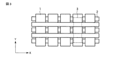
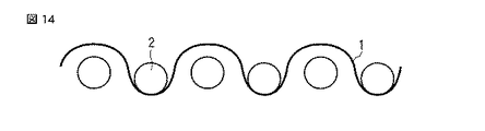
図1は、本発明の一実施形態に係る表示装置の表示面を概略的に示す斜視図である。図2に、図1に示す表示面のYZ平面の断面図を示す。
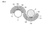
図20に、この場合の走査線の断面の詳細構造を示す。図20に示すように、光導波路2と光取出機能層13との間に第1スペーサ141を配置し、線状体6と第3電極124との間に第2スペーサ142を配置させた構成となっている。第1スペーサ141及び第2スペーサ142を介して両端を接着することにより、光導波路2と線状体6の配置関係を維持できるとともに、光導波路2及び線状体6と走査線にて形状を維持可能な表示面を形成することも可能である。このとき、第1スペーサ141及び第2スペーサ142は、光導波路2に接する面が光導波路2における全反射を妨げないような光導波路2よりも屈折率が低い材料や反射材料であることが望ましい。
図21において、上側に断面構成例、下側に平面構成例を示す。表示装置の画素に相当するサイズについては、用いる光導波路2と線状体6の太さと圧電体などから構成される走査線1の幅により規定できる。ここでは、図21に示すように、3本の光導波路2と3本の線状体6の計6本と、走査線1の幅から囲まれた領域が1画素の基本構成となり、図21において示すLが画素サイズに相当することになる。
図22は、このような構成における画素相当の断面構成例と平面構成例を示したものである。この場合、1つの光導波路2に光源から例えばR,G,B成分などを混ぜて入射可能であるため、従来の表示装置のように空間分割または時間分割による色分割を行う必要がない。このようにすると、例えば前述した画格が対角100インチで1920×1080の画素数をもつ表示装置を作製する場合、例えば、走査線幅は同様であるが、光導波路2と線状体6として断面が直径0.50mmとし、光導波路2と線状体6と間との間を0.075mmピッチで配置させることにより実現可能となる。ここでは精細度を対角100インチ相当で1920×1080の画素数としたが、本表示装置の精細度は、用いる光導波路2や線状体6の直径や走査線1の幅を変更することにより容易に変更可能である。なお、上記実施形態では、光導波路2と線状体6を同一形状としたが、同一形状でなくとも形成は可能である。
Claims (5)
- 列方向に沿って配列された、光取り出し領域を有する複数の光導波路と、
前記複数の光導波路に光を入射する複数の光源と、
行方向において凸部と凹部が交互に位置する断面を有し、前記凸部及び凹部のそれぞれの内面が前記光導波路に対向するように配置され、電界が印加されることにより前記凸部及び凹部が前記光導波路の光取り出し領域に応力を与えるように変位を生じる複数の走査線と、
前記複数の走査線に前記電界を順次印加する制御部と
を具備することを特徴とする表示装置。 - 前記走査線は、可撓性を有する少なくとも1つの圧電体層と、前記圧電体層を厚み方向の両側から挟むように配置された複数の電極層とを含み、前記制御部は前記複数の電極層間に前記電界を印加することを特徴とする請求項1記載の表示装置。
- 前記走査線は、前記凸部と前記凹部とで相異なる変位を生じ、前記凸部での変位と前記凹部での変位が低減可能であることを特徴とする請求項1記載の表示装置。
- 前記複数の光導波路の相互間に配置された光吸収性の線状体をさらに具備することを特徴とする請求項1記載の表示装置。
- 前記光導波路と前記走査線との間に配置されたスペーサをさらに具備することを特徴とする請求項1記載の表示装置。
Priority Applications (2)
| Application Number | Priority Date | Filing Date | Title |
|---|---|---|---|
| JP2008171601A JP5193704B2 (ja) | 2008-06-30 | 2008-06-30 | 表示装置 |
| US12/493,560 US8390610B2 (en) | 2008-06-30 | 2009-06-29 | Display apparatus with scanning lines having convex and concave portions |
Applications Claiming Priority (1)
| Application Number | Priority Date | Filing Date | Title |
|---|---|---|---|
| JP2008171601A JP5193704B2 (ja) | 2008-06-30 | 2008-06-30 | 表示装置 |
Publications (2)
| Publication Number | Publication Date |
|---|---|
| JP2010008965A true JP2010008965A (ja) | 2010-01-14 |
| JP5193704B2 JP5193704B2 (ja) | 2013-05-08 |
Family
ID=41446806
Family Applications (1)
| Application Number | Title | Priority Date | Filing Date |
|---|---|---|---|
| JP2008171601A Expired - Fee Related JP5193704B2 (ja) | 2008-06-30 | 2008-06-30 | 表示装置 |
Country Status (2)
| Country | Link |
|---|---|
| US (1) | US8390610B2 (ja) |
| JP (1) | JP5193704B2 (ja) |
Families Citing this family (3)
| Publication number | Priority date | Publication date | Assignee | Title |
|---|---|---|---|---|
| JP5367383B2 (ja) * | 2009-01-14 | 2013-12-11 | 株式会社東芝 | 表示装置及びその駆動方法 |
| JP5161934B2 (ja) | 2010-08-03 | 2013-03-13 | 株式会社東芝 | 表示素子および表示装置 |
| CN105629378B (zh) * | 2016-01-04 | 2018-03-16 | 京东方科技集团股份有限公司 | 显示基板以及显示装置 |
Citations (4)
| Publication number | Priority date | Publication date | Assignee | Title |
|---|---|---|---|---|
| JPS59148030A (ja) * | 1983-02-15 | 1984-08-24 | Sony Corp | 光フアイバ−デイスプレイ装置 |
| JP2001265265A (ja) * | 2000-03-15 | 2001-09-28 | Sony Corp | 表示装置 |
| JP2005221590A (ja) * | 2004-02-03 | 2005-08-18 | Seiko Epson Corp | 表示装置 |
| JP2005221589A (ja) * | 2004-02-03 | 2005-08-18 | Seiko Epson Corp | 表示装置 |
Family Cites Families (4)
| Publication number | Priority date | Publication date | Assignee | Title |
|---|---|---|---|---|
| JPH01185692A (ja) | 1988-01-19 | 1989-07-25 | Sanyo Electric Co Ltd | 平面ディスプレイパネル |
| JP4460732B2 (ja) * | 2000-07-21 | 2010-05-12 | 富士フイルム株式会社 | 平面表示装置および露光装置 |
| WO2004100118A1 (ja) * | 2003-05-07 | 2004-11-18 | Toshiba Matsushita Display Technology Co., Ltd. | El表示装置およびその駆動方法 |
| JP4282533B2 (ja) * | 2004-04-19 | 2009-06-24 | 株式会社東芝 | 表示装置 |
-
2008
- 2008-06-30 JP JP2008171601A patent/JP5193704B2/ja not_active Expired - Fee Related
-
2009
- 2009-06-29 US US12/493,560 patent/US8390610B2/en not_active Expired - Fee Related
Patent Citations (4)
| Publication number | Priority date | Publication date | Assignee | Title |
|---|---|---|---|---|
| JPS59148030A (ja) * | 1983-02-15 | 1984-08-24 | Sony Corp | 光フアイバ−デイスプレイ装置 |
| JP2001265265A (ja) * | 2000-03-15 | 2001-09-28 | Sony Corp | 表示装置 |
| JP2005221590A (ja) * | 2004-02-03 | 2005-08-18 | Seiko Epson Corp | 表示装置 |
| JP2005221589A (ja) * | 2004-02-03 | 2005-08-18 | Seiko Epson Corp | 表示装置 |
Also Published As
| Publication number | Publication date |
|---|---|
| US20090322736A1 (en) | 2009-12-31 |
| JP5193704B2 (ja) | 2013-05-08 |
| US8390610B2 (en) | 2013-03-05 |
Similar Documents
| Publication | Publication Date | Title |
|---|---|---|
| US7236663B2 (en) | Display element and display device using the same | |
| US8619210B2 (en) | Display device | |
| KR100861059B1 (ko) | 광변조 소자, 표시 소자 및 노광 소자 | |
| US8780015B2 (en) | Display device with image expansion via peripherial light guide elements | |
| US8797633B1 (en) | Display device assembly and manufacture thereof | |
| US20090027587A1 (en) | Planar lighting device and liquid crystal display device using the same | |
| CN102087814A (zh) | 一种无边框显示装置及大屏幕显示器 | |
| US20100053535A1 (en) | Display apparatus and method of fabrication the same | |
| JP2022524582A (ja) | 光制御フィルムを有する水平視差マルチビューディスプレイ及び方法 | |
| US20040240782A1 (en) | Light scattering optical resonator | |
| JP5193704B2 (ja) | 表示装置 | |
| TWI689758B (zh) | 具有方向性控制輸出之顯示裝置,及該顯示裝置的背光 | |
| JPWO2007013249A1 (ja) | 視差バリア、多重表示装置、及び視差バリアの製造方法 | |
| CN118317628A (zh) | 显示基板及其制备方法、显示面板 | |
| CN210691001U (zh) | 立体显示装置 | |
| CN103123425A (zh) | 液晶显示装置及其制造方法 | |
| CN115620613B (zh) | 量子点背光模组及显示装置 | |
| CN111837070A (zh) | 具有倾斜的多光束列的水平视差多视图显示器和方法 | |
| CN110212010B (zh) | 像素排布结构及显示面板 | |
| JP2007193288A (ja) | 薄膜トランジスターアレイおよび半透過型液晶表示パネル | |
| JP2009282102A (ja) | 液晶表示装置 | |
| JP4994649B2 (ja) | カラー液晶表示装置のバックライト | |
| CN114966927A (zh) | 防窥膜及拼接面板 | |
| JP2008164703A (ja) | 表示素子およびその製造方法 | |
| JP2001042777A (ja) | 表示装置 |
Legal Events
| Date | Code | Title | Description |
|---|---|---|---|
| A621 | Written request for application examination |
Free format text: JAPANESE INTERMEDIATE CODE: A621 Effective date: 20110323 |
|
| A977 | Report on retrieval |
Free format text: JAPANESE INTERMEDIATE CODE: A971007 Effective date: 20120808 |
|
| A131 | Notification of reasons for refusal |
Free format text: JAPANESE INTERMEDIATE CODE: A131 Effective date: 20120821 |
|
| A521 | Written amendment |
Free format text: JAPANESE INTERMEDIATE CODE: A523 Effective date: 20121017 |
|
| TRDD | Decision of grant or rejection written | ||
| A01 | Written decision to grant a patent or to grant a registration (utility model) |
Free format text: JAPANESE INTERMEDIATE CODE: A01 Effective date: 20130108 |
|
| A61 | First payment of annual fees (during grant procedure) |
Free format text: JAPANESE INTERMEDIATE CODE: A61 Effective date: 20130204 |
|
| FPAY | Renewal fee payment (event date is renewal date of database) |
Free format text: PAYMENT UNTIL: 20160208 Year of fee payment: 3 |
|
| LAPS | Cancellation because of no payment of annual fees |