JP2010004082A - Method of manufacturing semiconductor device - Google Patents
Method of manufacturing semiconductor device Download PDFInfo
- Publication number
- JP2010004082A JP2010004082A JP2009231557A JP2009231557A JP2010004082A JP 2010004082 A JP2010004082 A JP 2010004082A JP 2009231557 A JP2009231557 A JP 2009231557A JP 2009231557 A JP2009231557 A JP 2009231557A JP 2010004082 A JP2010004082 A JP 2010004082A
- Authority
- JP
- Japan
- Prior art keywords
- film
- layer
- contact hole
- plug
- adhesive layer
- Prior art date
- Legal status (The legal status is an assumption and is not a legal conclusion. Google has not performed a legal analysis and makes no representation as to the accuracy of the status listed.)
- Granted
Links
Images


Classifications
-
- H—ELECTRICITY
- H01—ELECTRIC ELEMENTS
- H01L—SEMICONDUCTOR DEVICES NOT COVERED BY CLASS H10
- H01L28/00—Passive two-terminal components without a potential-jump or surface barrier for integrated circuits; Details thereof; Multistep manufacturing processes therefor
- H01L28/40—Capacitors
- H01L28/60—Electrodes
-
- H—ELECTRICITY
- H10—SEMICONDUCTOR DEVICES; ELECTRIC SOLID-STATE DEVICES NOT OTHERWISE PROVIDED FOR
- H10B—ELECTRONIC MEMORY DEVICES
- H10B53/00—Ferroelectric RAM [FeRAM] devices comprising ferroelectric memory capacitors
-
- H—ELECTRICITY
- H10—SEMICONDUCTOR DEVICES; ELECTRIC SOLID-STATE DEVICES NOT OTHERWISE PROVIDED FOR
- H10B—ELECTRONIC MEMORY DEVICES
- H10B53/00—Ferroelectric RAM [FeRAM] devices comprising ferroelectric memory capacitors
- H10B53/30—Ferroelectric RAM [FeRAM] devices comprising ferroelectric memory capacitors characterised by the memory core region
-
- H—ELECTRICITY
- H01—ELECTRIC ELEMENTS
- H01L—SEMICONDUCTOR DEVICES NOT COVERED BY CLASS H10
- H01L21/00—Processes or apparatus adapted for the manufacture or treatment of semiconductor or solid state devices or of parts thereof
- H01L21/70—Manufacture or treatment of devices consisting of a plurality of solid state components formed in or on a common substrate or of parts thereof; Manufacture of integrated circuit devices or of parts thereof
- H01L21/71—Manufacture of specific parts of devices defined in group H01L21/70
- H01L21/768—Applying interconnections to be used for carrying current between separate components within a device comprising conductors and dielectrics
- H01L21/76838—Applying interconnections to be used for carrying current between separate components within a device comprising conductors and dielectrics characterised by the formation and the after-treatment of the conductors
- H01L21/76895—Local interconnects; Local pads, as exemplified by patent document EP0896365
Abstract
Description
本発明は、半導体素子及びその製造方法に関し、特に、キャパシタを備える半導体素子及びその製造方法に関する。 The present invention relates to a semiconductor device and a manufacturing method thereof, and more particularly to a semiconductor device including a capacitor and a manufacturing method thereof.
半導体素子の高集積化や小型化、高速化が進められるにつれ、キャパシタの占有面積が減少してきている。しかし、半導体素子の高集積化や小型化がなされても、駆動に必要なキャパシタの静電容量を確保する必要があり、そのための研究が進められている。 As semiconductor devices are highly integrated, miniaturized, and speeded up, the area occupied by capacitors is decreasing. However, even if semiconductor devices are highly integrated and miniaturized, it is necessary to ensure the capacitance of the capacitors necessary for driving, and research for that purpose is underway.
キャパシタの静電容量を確保するための一つの方法として、キャパシタの下部電極をシリンダー(Cyclinder)構造、スタック(Stack)構造、ピン(Pin)構造、凹状(Concave)構造などの多様な構造にして、制限された面積下でキャパシタ下部電極の有効表面積を拡大する方法がある。 As one method for securing the capacitance of the capacitor, the lower electrode of the capacitor is made into various structures such as a cylinder structure, a stack structure, a pin structure, and a concave structure. There is a method of expanding the effective surface area of the capacitor lower electrode under a limited area.
また、他の方法として、キャパシタ誘電体膜にBST、Ta2O5などの高誘電体膜や、SBTN((Sr、Bi)(Ta、Nb)2O9)、SBT((Sr、Bi)Ta2O9)、BLT((Bi、La)Ti3O12)のような強誘電体膜を用いる方法がある。なお、このような高誘電体膜や強誘電体膜を用いる場合、電気的特性面でキャパシタの上部電極や下部電極には、白金(Pt)、イリジウム(Ir)、ルテニウム(Ru)、イリジウム酸化膜(IrO)、ルテニウム酸化膜(RuO)、白金合金(Pt-alloy)、TiNなどの導電性膜が用いられている。 In addition, as another method, a capacitor dielectric film is made of a high dielectric film such as BST or Ta 2 O 5 , SBTN ((Sr, Bi) (Ta, Nb) 2 O 9 ), SBT ((Sr, Bi) There is a method using a ferroelectric film such as Ta 2 O 9 ) or BLT ((Bi, La) Ti 3 O 12 ). When using such a high dielectric film or ferroelectric film, platinum (Pt), iridium (Ir), ruthenium (Ru), iridium oxide is used for the upper and lower electrodes of the capacitor in terms of electrical characteristics. Conductive films such as a film (IrO), a ruthenium oxide film (RuO), a platinum alloy (Pt-alloy), and TiN are used.
このような導電性膜を用いてキャパシタ下部電極を形成する場合、ソース/ドレイン領域や、ワードライン、ビットラインのようなトランジスタ形成工程が完了した半導体基板上に、これらのトランジスタ等に接続されたストレージノードコンタクトプラグを先に形成しておき、該ストレージノードコンタクトプラグに接続された下部電極を形成して得られるPP(Polysilicon Plug)構造が広く用いられている。 When the capacitor lower electrode is formed using such a conductive film, the transistor is connected to the source / drain region and the semiconductor substrate on which the transistor formation process such as the word line and the bit line has been completed. A PP (Polysilicon Plug) structure obtained by forming a storage node contact plug in advance and forming a lower electrode connected to the storage node contact plug is widely used.
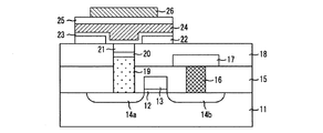
図1A及び図1Bは、従来の技術に係る半導体素子の一製造過程における素子の構造を示す断面図である。 FIG. 1A and FIG. 1B are cross-sectional views showing the structure of an element in one manufacturing process of a semiconductor element according to the prior art.
図1Aに示すように、まず半導体基板11上にゲート酸化膜12及びワードライン13を形成する。
As shown in FIG. 1A, a
引き続いて、ワードライン13両側の半導体基板11の表層部に不純物をイオン注入してソース14a及びドレイン14b(またはドレイン領域14a及びソース領域14b)を形成した後、半導体基板11及びワードライン13の上面に第1層間絶縁膜15を形成する。
Subsequently, impurities are ion-implanted into the surface layer portion of the
次いで、第1層間絶縁膜15をパターニングして、ドレイン領域14bを露出する第1コンタクトホールを形成した後、第1コンタクトホール内及び第1層間絶縁膜15の上面にタングステン層を成長させる。
Next, after patterning the first
次いで、第1層間絶縁膜15の上面が露出するまで、タングステン層をエッチバック法または化学機械的研磨(Chemical Mechanical Polishing;CMP)法等で平坦化して第1コンタクトホール内に埋め込まれたビットラインコンタクト、すなわちタングステンプラグ16を形成する。
Next, the tungsten layer is planarized by an etch-back method or a chemical mechanical polishing (CMP) method or the like until the upper surface of the first
そして、タングステンプラグ16及び第1層間絶縁膜15の上面にビットライン用導電膜を成長させた後、パターニングしてタングステンプラグ16を介してドレイン14bに接続されたビットライン17を形成する。このようにして、トランジスタ製造工程を実施しておく。
Then, after a bit line conductive film is grown on the top surface of the
次いで、ビットライン17及び第1層間絶縁膜15の上面に、第2層間絶縁膜18を成長させて平坦化した後、パターニングした感光膜(図示せず)をマスクとして、第2層間絶縁膜18と第1層間絶縁膜15とをエッチングし、ソース領域14aの表面を露出する第2コンタクトホールを形成する。この第2コンタクトホールは、通常ストレージノードコンタクトホール(Storage Node Contact hole)と呼ばれる。
Next, a second
次いで、第2コンタクトホール内及び第2層間絶縁膜18の上面にポリシリコン層を成長させた後、エッチバック法やCMP法により第2コンタクトホール内の上方部分に隙間を有して埋め込まれたポリシリコンプラグ19を形成する。
Next, after a polysilicon layer is grown in the second contact hole and on the upper surface of the second
次いで、ポリシリコンプラグ19及び第2層間絶縁膜18上にチタニウム(Ti)を成長させ、急速熱処理(Rapid Thermal Process;RTP)を施して、ポリシリコンプラグ19のシリコン(Si)とチタニウム(Ti)とを反応させて、ポリシリコンプラグ19の上面にチタニウムシリサイド(Ti-Si)膜20を形成する。このチタニウムシリサイド膜20は、ポリシリコンプラグ19と下部電極との間でオーミックコンタクトを形成する役割を果たす。
Next, titanium (Ti) is grown on the
次に、ウェットエッチング等で未反応のチタニウムを除去し、チタニウムシリサイド膜20及び第2層間絶縁膜18の上面にチタニウムナイトライド(TiN)層を成長させた後、第2層間絶縁膜18の表面が露出されるまでチタニウムナイトライド層をエッチバック法やCMP法で平坦化して、第2コンタクトホール内に完全に埋め込まれたチタニウムナイトライド膜21を形成する。このチタニウムナイトライド膜21は、ポリシリコンプラグ19と下部電極との間の相互拡散を防止するバリヤ層として作用する。
Next, unreacted titanium is removed by wet etching or the like, a titanium nitride (TiN) layer is grown on the upper surfaces of the
次いで、チタニウムナイトライド膜21及び第2層間絶縁膜18の上面に接着層22を形成した後、接着層22をパターニングして、チタニウムナイトライド膜21を露出させる第3コンタクトホールを形成する。
Next, after forming the
この第3コンタクトホールは、非導電性の接着層22を貫通して、後続する拡散バリヤ膜とチタニウムナイトライド膜21とを電気的に接続させるために、チタニウムナイトライド膜21が埋め込まれた第2コンタクトホールより広い幅で形成される。なお、接着層22は、下部電極と第2層間絶縁膜18との間の接着力を強化するためのものであって、この接着層22にはIrO2等が用いられる。
This third contact hole penetrates the non-conductive
次に、図1Bに示すように、第3コンタクトホールが形成された接着層22、チタニウムナイトライド膜21及び第2層間絶縁膜18の上面に拡散バリヤ膜23、下部電極24、誘電体膜25、上部電極26を形成するための層を順に成長させた後、上部電極26を先にパターニングして形成し、次いで誘電体膜25、下部電極24、拡散バリヤ膜23及び接着層22を順にパターニングして形成する。このようにしてキャパシタ構造を形成する。
Next, as shown in FIG. 1B, a
上述したような構造はCOB(Capacitor Over Bitline)構造といわれるが、この構造では、ポリシリコンプラグ19、チタニウムシリサイド膜20及びチタニウムナイトライド21からなるストレージノードコンタクト(SNC)を形成する工程、及び該ストレージノードコンタクトに接続される拡散バリヤ膜23を形成する工程が極めて重要である。
The structure as described above is called a COB (Capacitor Over Bitline) structure. In this structure, a process of forming a storage node contact (SNC) composed of the
ストレージノードコンタクトを形成する工程では、後続する誘電体膜25の結晶化の際に必須の高温熱処理時に十分な耐熱特性を有する構造を形成することが要求される。
In the process of forming the storage node contact, it is required to form a structure having sufficient heat resistance characteristics during the high-temperature heat treatment that is essential for the subsequent crystallization of the
また、該誘電体膜25を形成する際の下層となる拡散バリヤ膜23を形成する工程では、拡散バリヤ膜23の上面が十分に平坦であることが要求される。これは、誘電体膜25を有機金属気相成長法(Metal Organic Chemical Vapor Deposition;MOCVD法)や、ゾル-ゲル(Sol-gel)法により形成する場合、特に重要となる。
Further, in the step of forming the
しかし、拡散バリヤ膜23とプラグとの間を接着するためには、接着層22が必要であり、これによって、拡散バリヤ膜23の平坦性が損なわれていた。その理由は、接着層22の開口によってトポロジー(topology)、すなわち段差が発生し、後続する強誘電体膜の成長時に悪影響を与えていたためである。この弊害を抑えるために、接着層22を薄膜化することによって平坦性を確保することが試みられた。拡散バリヤ膜23の平坦性は、接着層22の厚さが薄ければ薄いほど良くなるからである。
However, in order to bond the
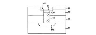
図2は、図1Aに示した第3コンタクトホールを形成したときの素子の構造をより詳細に示す断面図である。 FIG. 2 is a sectional view showing in more detail the structure of the element when the third contact hole shown in FIG. 1A is formed.
上述したように、薄膜化された接着層22を成長させると、次に、エッチングによりチタニウムナイトライド膜21を露出させる上記第3コンタクトホールを形成する。この場合、第2層間絶縁膜18に対する接着層22のエッチング選択比、及びチタニウムナイトライド膜21に対する接着層22のエッチング選択比を高くするエッチング条件でエッチングを行うことが必要となる。これは、接着層22の上面と第2層間絶縁膜18及びチタニウムナイトライド膜21の上面との間の段差を小さくし、後続する誘電体膜25の成長時にトポロジーによる弊害を抑えるためである。
As described above, when the thinned
しかし、一般的に拡散バリヤ膜23には IrOx/Irの積層構造が用いられ、接着層22には、IrO2が用いられる。IrO2は、その接着特性こそ十分であるが、反応性の低い物質であるため、これをパターニングするときのエッチングは物理的な方法に限られる。したがって、第3コンタクトホール形成時のエッチングにおけるエッチング選択比は低いものに限られてしまう。その結果、被エッチング膜である接着層22をエッチングした後、マージン確保のために行うオーバエッチングでは、図示したようにチタニウムナイトライド膜21に対する第2層間絶縁膜18のエッチング選択比が高くなるなどの不具合が生じてしまい、チタニウムナイトライド膜21のメサ状構造を内部に有するトレンチAが第2層間絶縁膜18表層部に形成されてしまう等、拡散バリヤ膜23の平坦性を実現するには限界があった。
However, in general, a laminated structure of IrO x / Ir is used for the
そのため、後続する誘電体膜25を成長させる際に、トポロジーのために誘電体膜25の厚さが不均一となってしまい、誘電体膜25に熱処理を施す際にクラックなどが発生しやすくなり、また誘電体膜25のパターニングが困難になるという問題があった。
Therefore, when the subsequent
さらに、トポロジーにより、上記熱処理工程において、拡散バリヤ膜23とストレージノードコンタクトとの接触状態や、誘電体膜25と下部電極24との接着状態に異常が発生し、メモリ素子においてエラーが発生するなど、強誘電体膜のキャパシタを備えた半導体素子はもちろん、熱処理工程が必要な誘電体膜のキャパシタを備えた全ての半導体素子において、安定したキャパシタ特性を実現するのが困難であるという問題があった。
Further, depending on the topology, in the above heat treatment process, an abnormality occurs in the contact state between the
本発明は、上述した従来の技術が有する問題点を解決するためになされたものであって、トポロジーの発生を抑え、これにより、キャパシタの下部電極の平坦性を確保し、キャパシタ特性を安定化させることができる半導体素子の製造方法を提供することを目的としている。 The present invention has been made to solve the above-described problems of the prior art, and suppresses the generation of topology, thereby ensuring the flatness of the lower electrode of the capacitor and stabilizing the capacitor characteristics. It is an object of the present invention to provide a method of manufacturing a semiconductor device that can be made to operate.
また、本発明は、上述したような接着層を用いる際にトポロジーの発生を抑制しつつ、プラグ、オーミックコンタクト層及びバリヤ層からなる接続部の耐酸化特性を向上させることができる半導体素子の製造方法を提供することを目的としている。 Further, the present invention provides a semiconductor device capable of improving the oxidation resistance characteristics of a connection portion composed of a plug, an ohmic contact layer, and a barrier layer while suppressing the occurrence of topology when using the adhesive layer as described above. It aims to provide a method.
本発明に係る半導体素子の製造方法は、トランジスタが形成された半導体基板上面に層間絶縁膜を成長させる層間絶縁膜成長工程と、前記層間絶縁膜をパターニングして、前記半導体基板の所定領域の表面を露出させる層間膜コンタクトホールを形成する層間膜コンタクトホール形成工程と、前記層間膜コンタクトホール内、及び前記層間絶縁膜の上面に、シリコン含有物質からなるプラグ埋込層を成長させ、前記層間膜コンタクトホール内にプラグを形成するプラグ形成工程と、前記プラグ及び前記層間絶縁膜の上面に形成された前記プラグ埋込層をエッチバック法で平坦化するプラグ埋込層平坦化工程と、前記プラグ及び前記層間絶縁膜の上面に所定の厚さを有する反応予備膜を形成する反応予備膜形成工程と、前記反応予備膜の上面にイリジウム含有物質を含むイリジウム反応層を成長させ、前記反応予備膜のシリコンと前記イリジウム反応層のイリジウムとを反応させて、前記プラグ及び前記層間絶縁膜の上面に、シリコン及びイリジウムを含有する接着層を成長させる接着層成長工程と、前記接着層をパターニングして、前記プラグの上面を露出させる接着層コンタクトホールを形成する接着層コンタクトホール形成工程と、前記接着層コンタクトホール内、及び前記接着層上面に導電性のバリヤ埋込層を成長させるバリヤ埋込層成長工程と、前記接着層の表面が露出するまで、前記バリヤ埋込層を平坦化して、前記バリヤ層を形成するバリヤ埋込層平坦化工程と、前記バリヤ層及び前記接着層の上面に第1電極と、誘電体膜と、第2電極とを含んで構成されるキャパシタを形成するキャパシタ形成工程とを含むことを特徴としている。 A method of manufacturing a semiconductor device according to the present invention includes: an interlayer insulating film growth step for growing an interlayer insulating film on a semiconductor substrate on which a transistor is formed; and patterning the interlayer insulating film to form a surface of a predetermined region of the semiconductor substrate An interlayer film contact hole forming step for forming an interlayer film contact hole to expose the plug, and a plug buried layer made of a silicon-containing material is grown in the interlayer film contact hole and on the upper surface of the interlayer insulating film, A plug forming step of forming a plug in the contact hole, a plug embedded layer planarizing step of planarizing the plug embedded layer formed on the plug and the upper surface of the interlayer insulating film by an etch back method, and the plug And a reaction preliminary film forming step of forming a reaction preliminary film having a predetermined thickness on the upper surface of the interlayer insulating film, and an upper surface of the reaction preliminary film An adhesive layer containing silicon and iridium is formed on the plug and the upper surface of the interlayer insulating film by growing an iridium reaction layer containing a lithium-containing material and reacting silicon of the preliminary reaction film with iridium of the iridium reaction layer. An adhesive layer growth step for patterning the adhesive layer, an adhesive layer contact hole forming step for patterning the adhesive layer to expose an upper surface of the plug, and in the adhesive layer contact hole and the adhesive layer A barrier buried layer growth step for growing a conductive barrier buried layer on the upper surface; and a barrier buried layer for planarizing the barrier buried layer until the surface of the adhesive layer is exposed to form the barrier layer. A capacity comprising a planarization step and a first electrode, a dielectric film, and a second electrode on the top surface of the barrier layer and the adhesive layer; It is characterized in that it comprises a capacitor formation step of forming a.
ここで、前記接着層形成工程を、前記接着層形成工程を、約500℃〜約800℃の温度範囲で前記イリジウム反応層を成長させる条件で行うことが望ましい、その後、約500℃〜約800℃の温度範囲での熱処理を、少なくとも一回以上施して行うこともできる。 Here, the adhesive layer forming step is preferably performed under conditions where the adhesive layer forming step grows the iridium reaction layer in a temperature range of about 500 ° C. to about 800 ° C., and then about 500 ° C. to about 800 ° C. The heat treatment in the temperature range of ° C. can be performed at least once.
また、前記プラグ形成工程が、前記プラグ埋込層としてポリシリコン層を成長させることが望ましい。 In the plug forming step, a polysilicon layer is preferably grown as the plug buried layer.
また、前記反応予備膜を、約10Å〜約1000Åの範囲内の厚さに形成することが望ましい。 In addition, it is desirable to form the preliminary reaction film to a thickness in the range of about 10 to about 1000 mm.
また、前記バリヤ埋込層平坦化工程を、CMP法により、前記バリヤ層と前記接着層との研磨選択比が約50:1〜80:1の範囲内となる条件で行うことが望ましい。 Further, it is preferable that the barrier buried layer flattening step is performed by a CMP method under a condition that a polishing selection ratio between the barrier layer and the adhesive layer is in a range of about 50: 1 to 80: 1.
また、前記キャパシタ形成工程が、前記第1電極を形成する第1電極形成工程と、前記第2電極を形成する第2電極形成工程とを含み、前記第1電極形成工程または前記第2電極形成工程が、TiN、RuTiN、IrTiN、Ir、IrOx、Ru、RuOx、Rh、RhOx、Pt及びこれらを組み合わせたもののうち、いずれかの物質を成長させる処理を含むことが望ましい。 The capacitor forming step includes a first electrode forming step for forming the first electrode and a second electrode forming step for forming the second electrode, wherein the first electrode forming step or the second electrode forming step is performed. It is desirable that the process includes a process of growing any one of TiN, RuTiN, IrTiN, Ir, IrO x , Ru, RuO x , Rh, RhO x , Pt, and combinations thereof.
本発明によれば、トポロジーの発生を抑え、これによって、キャパシタの下部電極の平坦性を確保し、キャパシタ特性を安定化させることができる。したがって、下部電極と誘電体膜の有効接触面積を増加させて、素子の電気特性を向上させることができる。また、キャパシタから出る電荷量の制御を容易にすることができ、それにより、素子の特性を均一にすることができる。 According to the present invention, it is possible to suppress the occurrence of topology, thereby ensuring the flatness of the lower electrode of the capacitor and stabilizing the capacitor characteristics. Therefore, the effective contact area between the lower electrode and the dielectric film can be increased, and the electrical characteristics of the device can be improved. In addition, it is possible to easily control the amount of charge emitted from the capacitor, thereby making the device characteristics uniform.
また、本発明によれば、拡散バリヤ膜を均一に形成することができ、誘電体膜の結晶化のための熱処理での耐熱特性を高め、またプラグ及びバリヤ層の酸化を防止することができ、製造工程を安定化させることができるという優れた効果がある。 In addition, according to the present invention, the diffusion barrier film can be formed uniformly, the heat resistance characteristics in the heat treatment for crystallization of the dielectric film can be improved, and the oxidation of the plug and the barrier layer can be prevented. There is an excellent effect that the manufacturing process can be stabilized.
以下、添付した図面を参照しながら、本発明に係る実施の形態を詳しく説明する。 Hereinafter, embodiments of the present invention will be described in detail with reference to the accompanying drawings.
図3は、本発明の第1の実施の形態に係る半導体素子の構造を示す断面図である。ここでは、半導体素子のうち半導体基板に接続されたキャパシタの部分のみを示している。 FIG. 3 is a cross-sectional view showing the structure of the semiconductor device according to the first embodiment of the present invention. Here, only the capacitor portion connected to the semiconductor substrate in the semiconductor element is shown.
図3に示すように、本発明の実施の形態に係る半導体素子は、基礎導電膜となる半導体基板31と、層間膜コンタクトホールとなる第1コンタクトホールを有し、半導体基板31上面に形成された層間絶縁膜32と、前記第1コンタクトホールと連続した接着層コンタクトホールとなる第2コンタクトホールを有し、層間絶縁膜32上面に形成された接着層34と、接着層34及び層間絶縁膜32を貫通した、前記第1コンタクトホール及び前記第2コンタクトホールからなる複合コンタクトホール内に、半導体基板31に接続され、接着層34の上面に合わせて平坦化されて形成された接続部100と、接続部100及び接着層34の上面に形成された第1電極となる拡散バリヤ膜37及び下部電極38の積層構造と、第1電極上面に形成された誘電体膜39と、誘電体膜39上面に形成された第2電極となる上部電極40とを備えたキャパシタを含んで構成されている。
As shown in FIG. 3, the semiconductor element according to the embodiment of the present invention has a
接着層34は、イリジウムとシリコンとが含まれた金属膜、例えばイリジウムシリサイド(IrSix) (x=1〜2)に限らず、イリジウム酸化膜(IrO2)、Al2O3、Ta2O5、TiOx(x=1〜2)、ZrOx(x=1〜2)、HfOx(x=1〜2)及びこれらを組み合わせたもののうち、いずれかを含んで構成されていることが望ましい。
The
また、本実施の形態では、接続部100は、半導体基板31上に形成されたプラグとなるポリシリコンプラグ33、オーミックコンタクト層となるチタニウムシリサイド膜35、及びバリヤ層となるチタニウムナイトライド膜36aを含んで構成されており、接続部100の上面となるチタニウムナイトライド膜36aの上面は、接着層34の上面とほぼ同じ高さとなっている。
Further, in the present embodiment, the
本実施の形態では接続部100のプラグとして、ポリシリコンを用いているが、別の実施の形態では、タングステン(W)、タングステンシリサイド(W-Si)、TiN、TiAlN、TaSiN、TiSiN、TaN、TaAlN、TiSi、TaSi及びこれらを組み合わせたもののうち、いずれかを含んで構成されていてもよい。
In this embodiment, polysilicon is used as the plug of the
また、接続部100のバリヤ層は、本実施の形態で用いたチタニウムナイトライド(TiN)に限らず、TaNのような二元系窒化膜、TiSiN、TiAlN及びRuTiNのような三元系窒化膜、RuTiO及びこれらを組み合わせたもののうち、いずれかを含んで構成されていてもよい。
The barrier layer of the
そして、接続部100のオーミックコンタクト層は、本実施の形態で用いたチタニウムシリサイドに限らず、CoSiや、MoSi等をを含んで構成されていてもよい。
The ohmic contact layer of the
一方、層間絶縁膜32は、BSG(Boron Silicate Glass)膜、BPSG(Boron PhosphoSilicate Glass) 膜、HDP(High Density Plasma)酸化膜、USG(Undoped SilicateGlass) 膜、TEOS(Tetra Ethyl Ortho Silicate) 膜、APL(advanced planarization layer)酸化膜、SOG(Spin On Glass) 膜及びこれらを組み合わせた積層膜のうち、いずれかを含んで構成されていることが望ましい。
On the other hand, the
また、第1電極となる拡散バリヤ膜37及び下部電極38の積層構造、及び第2電極となる上部電極40は、Pt、Ir、IrOx、Ru、RuOx、Rh、RhOx、CaRuO3、SrRuO3、BaRuO3、BaSrRuO3、CaIrO3、SrIrO3、BaIrO3、(La、Sr)CoO3、Cu、Al、Ta、Mo、W、Au、Ag、WSi2、TiSi2、MoSix(x=0.3〜2)、CoSix(x=1〜2)、NbSix(x=0.3〜2)、TaSix(x=1〜2)、TiN、TaN、WN、TiSiN、TiAlN、TiBN、ZrSiN、ZrAlN、MoSiN、MoAlN、RuTiN、IrTiN、TaSiN、TaAlN、Os、OsOx(x=1〜2)、Pd、PdOx(x=1〜2)及びこれらを組み合わせたもののうち、いずれかを含んで構成されていることが望ましい。
The laminated structure of the
また、誘電体膜39としては、Ta2O5、STO(SrTiO3)、BST、PZT、PLZT((Pb、La)(Zr、Ti)O3)、BTO(BaTiO3)、PMN(Pb(Ng1/3Nb2/3)O3)、SBTN((Sr、Bi)(Ta、Nb)2O9)、SBT((Sr、Bi)Ta2O9)、BLT((Bi、La)Ti3O12)、PT(PbTiO3)及びこれらを組み合わせたもののうち、いずれかを含んで構成されていることが望ましい。
As the
図4A〜図4Eは、図3に示した半導体素子の一製造工程における素子の構造を示す断面図である。図示していないが、半導体基板31にはワードライン、ソース及びドレインを備えたトランジスタや、ビットラインコンタクト、ビットラインが形成されており、このことは以下においても同様である。
4A to 4E are cross-sectional views showing the structure of the element in one manufacturing process of the semiconductor element shown in FIG. Although not shown, a transistor having a word line, a source and a drain, a bit line contact, and a bit line are formed on the
まず、層間絶縁膜成長工程として、上記トランジスタ等が形成された半導体基板31上面に層間絶縁膜32を成長させて、半導体基板31表面におけるトランジスタ等の凹凸形状(図示せず)を埋め込んで平坦化する。
First, as an interlayer insulating film growth step, an
次いで、層間膜コンタクトホール形成工程として、層間絶縁膜32をパターニングして、半導体基板31に形成されたソース領域やドレイン領域等の所定領域の表面を露出する層間膜コンタクトホールとして第1コンタクトホールを形成する。
Next, as an interlayer film contact hole forming step, the
次に、プラグ形成工程のプラグ埋込層成長工程として、第1コンタクトホール内、及び層間絶縁膜32の上面に、シリコン含有物質からなる導電性のプラグ埋込層33を成長させる。本実施の形態では、プラグ埋込層33としてポリシリコン層を成長させ、第1コンタクトホール内に埋め込まれ、半導体基板31に接続されたポリシリコンプラグ33aと、該ポリシリコンプラグ33a及び層間絶縁膜32の上面に所定の厚さを有する反応予備膜33bとを形成する。
Next, as a plug buried layer growth step of the plug formation step, a conductive plug buried
このプラグ埋込層成長工程を、プラグ埋込層を、化学気相成長法(CVD法)、物理気相成長法(PVD法)、原子層成長法(ALD法)及びこれらを組み合わせた成長法のうち、いずれかの成長法を用いて成長させて行うことが望ましい。 In this plug buried layer growth step, the plug buried layer is grown by chemical vapor deposition (CVD), physical vapor deposition (PVD), atomic layer deposition (ALD) or a combination of these. Of these, it is desirable to perform growth using any one of the growth methods.
しかし、ポリシリコン層を成長させるだけではプラグ埋込層33における反応予備膜33bの厚さや平坦性を十分に制御できない場合がある。プラグ埋込層33における反応予備膜33bは、後にイリジウムと反応させるので、このとき膜全体が反応するのに適した所定の厚さで形成されることが望ましい。
However, in some cases, the thickness and flatness of the reaction
そのため、上記のような場合には、反応予備膜が厚めになるようにプラグ埋込層33を成長させた後、プラグ形成工程のプラグ埋込層平坦化工程として、ポリシリコンプラグ33a及び層間絶縁膜32上面のプラグ埋込層33をエッチバック法で平坦化することが望ましい。
Therefore, in the above case, after the plug buried
以上のようにして、反応予備膜33bをコンタクトホールの外側の層間絶縁膜32上面に、約10Å〜約1000Åの範囲内の厚さで形成することが望ましい。
As described above, it is desirable to form the
次いで、接着層成長工程として、反応予備膜33bの上面にイリジウム含有物質を含むイリジウム反応層(図示せず)を成長させ、反応予備膜33bのシリコンと前記イリジウム反応層のイリジウムとを反応させて、図4Bに示すように、ポリシリコンプラグ33a及び層間絶縁膜32の上面に、シリコン及びイリジウムを含有するイリジウムシリサイド(IrSix)からなる接着層34を成長させる。このとき、前記第1コンタクトホール内のポリシリコンプラグ33aが残留する。なお、本実施の形態では、イリジウム含有物質としてイリジウムを用いている。
Next, as an adhesion layer growth step, an iridium reaction layer (not shown) containing an iridium-containing material is grown on the upper surface of the reaction
この接着層成長工程を、約500℃〜約800℃の温度範囲でイリジウム反応層を成長させるとともに、反応予備膜33bのシリコンとイリジウムとを反応させて行うことが望ましい。
It is desirable to perform this adhesion layer growth step by growing an iridium reaction layer in a temperature range of about 500 ° C. to about 800 ° C. and reacting silicon of the
この場合、上述のように反応予備膜33bを所定の厚さにしておくと、層間絶縁膜32と接着層34との間にポリシリコンは残留しない。
In this case, if the reaction
接着層34は、特に、SiO2系の層間絶縁膜32との間で優れた接着力を有し、また、イリジウムが含まれた拡散バリヤ膜及び下部電極との間でも優れた接着力を有する。これは、層間絶縁膜32がシリコンを、拡散バリヤ膜及び下部電極がイリジウムを各々成分に有しているからである。
The
本実施の形態では、接着層成長工程を、イリジウムを約500℃〜約800℃の温度範囲で成長させるとともに反応予備膜33bのシリコンとイリジウムとを反応させて行っているが、接着層成長工程を、約500℃〜約800℃の温度範囲で前記イリジウム反応層を成長させる条件で行った後、約500℃〜約800℃の温度範囲での熱処理を、少なくとも一回以上施して行うこともできる。
In the present embodiment, the adhesive layer growth step is performed by growing iridium in a temperature range of about 500 ° C. to about 800 ° C. and reacting silicon and iridium in the reaction
なお、上記のようにイリジウムシリサイドを形成する場合、イリジウムとシリコンとの組成比は熱処理の温度や雰囲気により決定され、組成によって電気導電性に差が生じる。 When iridium silicide is formed as described above, the composition ratio between iridium and silicon is determined by the temperature and atmosphere of the heat treatment, and the electrical conductivity varies depending on the composition.
次に、接着層コンタクトホール形成工程として、図4Cに示すように、接着層34をパターニングして、ポリシリコンプラグ33aの上面を露出させる第2コンタクトホールを形成する。
Next, as a bonding layer contact hole forming step, as shown in FIG. 4C, the
次いで、バリヤ層形成工程として、図4Dに示すように、第2コンタクトホール内に、ポリシリコンプラグ33aに接続され、接着層34の上面に合わせて平坦化された、チタニウムシリサイド膜35とチタニウムナイトライド膜36aとの積層構造からなるバリヤ層を形成する。
Next, as a barrier layer forming step, as shown in FIG. 4D, the
まず、第2コンタクトホール内及び接着層34の上面にチタニウム層(図示せず)を成長させ、急速熱処理(RTP)を施して、ポリシリコンプラグ33aのシリコンとチタニウム層のチタニウムとを反応させて、ポリシリコンプラグ33a上面にチタニウムシリサイド(Ti-Si)膜35を形成する。チタニウムシリサイド膜35は、ポリシリコンプラグ33aと第1電極との間にオーミックコンタクトを形成する役割を果たす。
First, a titanium layer (not shown) is grown in the second contact hole and on the upper surface of the
次いで、ウェットエッチング等で未反応のチタニウムを除去した後、バリヤ層形成工程のバリヤ埋込層成長工程として、図4Cに示すように、第2コンタクトホール内のチタニウムシリサイド膜35上面、及び接着層34上面に、導電性のバリヤ埋込層としてチタニウムナイトライド(TiN)層36を成長させる。このようにバリヤ層形成工程は、TiN、TaN、TiSiN、TiAlN、RuTiN、RuTiO及びこれらを組み合わせたもののうち、いずれかの物質を成長させる処理を含むことが望ましい。
Next, after removing unreacted titanium by wet etching or the like, as shown in FIG. 4C, an upper surface of the
そして、バリヤ層形成工程のバリヤ埋込層平坦化工程として、図4Dに示すように、接着層34の表面が露出するまで、チタニウムナイトライド層36をCMP法で平坦化して、第2コンタクトホールに埋め込まれたバリヤ層となるチタニウムナイトライド膜36aを形成する。
Then, as a barrier buried layer flattening step of the barrier layer forming step, the
このバリヤ埋込層平坦化工程を、チタニウムナイトライド膜36aと接着層34との研磨選択比が約50:1〜80:1の範囲内となる条件で行うことが望ましく、そのため、スラリーなどの研磨条件を設定し、CMP法による接着層34の損失を低減させるとよい。
It is desirable to perform this barrier buried layer planarization step under the condition that the polishing selection ratio between the
このチタニウムナイトライド膜36aは、コンタクト抵抗を低下させ、拡散防止特性を向上させるという役割を果たす。そのためには、チタニウムナイトライド膜36aを50Å〜5000Åの範囲内の厚さで形成することが好ましく、またN2、N2O、NH3及びO2のうち、いずれかのガス雰囲気中でプラズマ処理を施すことによって、酸化防止特性をより一層向上させることができる。
The
次に、キャパシタ形成工程として、図4Eに示すように、チタニウムナイトライド36a及び接着層34の上面に第1電極となる拡散バリヤ膜37及び下部電極38と、誘電体膜39と、第2電極となる上部電極40とを含んで構成されるキャパシタを形成する。
Next, as a capacitor forming step, as shown in FIG. 4E, a
本実施の形態では、誘電体膜39を、MOCVD法、ゾル-ゲル法、スピンオン法、CVD法、ALD法、PVD法及びこれらを組み合わせた成長法のうち、いずれか一つの成長法により成長させることが望ましい。そして、拡散バリヤ膜37、下部電極38及び上部電極40を、MOCVD法、CVD法、ALD法、PVD法及びこれらを組み合わせた成長法のうち、いずれかの成長法により成長させることが望ましい。
In the present embodiment, the
次いで、上部電極40を先にパターニングし、誘電体膜39、下部電極38、拡散バリヤ膜37及び接着層34を順にパターニングして、下部電極38の幅が上部電極40の幅より広いキャパシタを形成する。
Next, the
この場合、誘電体膜39をパターニングした後、300℃〜850℃で一回以上の熱処理を施し、キャパシタを形成した後に、キャパシタの特性を向上させるために窒素を含んだガス雰囲気、例えばアンモニア(NH3)雰囲気下でプラズマ処理を施すことが望ましい。
In this case, after patterning the
例えば、誘電体膜39をパターニングした後、300℃〜500℃の温度範囲で、プラズマ熱処理またはUV-O3熱処理を施して、膜内の酸素の欠乏を十分に補う。その後、500℃〜850℃の温度範囲で急速熱処理(RTP)、または通常の熱処理を施して、膜内に残留する炭素、水素などの不純物を除去する。これにより、優れた誘電体特性を得ることができる。
For example, after patterning the
図5は、本発明の第2の実施の形態に係る半導体素子の構造を示す断面図である。 FIG. 5 is a cross-sectional view showing the structure of a semiconductor device according to the second embodiment of the present invention.
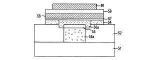
図5に示すように、本発明の第2の実施の形態に係る半導体素子は、基礎導電膜となる半導体基板51と、層間膜コンタクトホールとなる第3コンタクトホールを有し、半導体基板51上面に形成された層間絶縁膜52と、前記第3コンタクトホールと連続した接着層コンタクトホールとなる第4コンタクトホールを有し、層間絶縁膜52上面に形成された接着層54と、接着層54及び層間絶縁膜52を貫通した、前記第3コンタクトホール及び前記第4コンタクトホールからなる複合コンタクトホール内に半導体基板51に接続され、接着層54の上面に合わせて平坦化されて形成された接続部200と、接続部200及び接着層54の上面に形成された第1電極となる拡散バリヤ膜57及び下部電極58の積層構造、第1電極上面に形成された誘電体膜59、及び誘電体膜59上面に形成された第2電極となる上部電極60を備えたキャパシタを含んで構成されている。
As shown in FIG. 5, the semiconductor element according to the second embodiment of the present invention has a
本実施の形態では、図示したように、コンタクトホールの形状が図3に示したものと大きく異なっている。すなわち、接着層コンタクトホールとなる第4コンタクトホールは、層間膜コンタクトホールとなる第3コンタクトホールより広い幅を有し、層間絶縁膜52の上部を窪ませる絶縁膜凹部を備えている。
In the present embodiment, as shown in the figure, the shape of the contact hole is greatly different from that shown in FIG. That is, the fourth contact hole serving as the adhesive layer contact hole has a wider width than the third contact hole serving as the interlayer film contact hole, and includes an insulating film recess that allows the upper part of the
これにより、接続部200は、第3コンタクトホール内に形成されたプラグとなるポリシリコンプラグ53と、絶縁膜凹部を含む第4コンタクトホール内に形成されたオーミックコンタクト層となるチタニウムシリサイド膜55及びバリヤ層となるチタニウムナイトライド膜56aとを含んで構成されている。そして、接続部200の上端面となるチタニウムナイトライド膜56aは、接着層34の上面とほぼ同じ高さとなっており、また、ポリシリコンプラグ53に比べてその幅がより広くなっている。すなわち、接続部200は、その上面の面積が底面の面積に比べてより広くなっている。
As a result, the
しかし、本実施の形態における接着層54、接続部200、層間絶縁膜52、第1電極となる拡散バリヤ膜57及び下部電極58、第2電極となる上部電極60、及び誘電体膜59等を構成する物質については、図3に示したものと同様である。
However, the
図6A〜図6Eは、図5に示した半導体素子の一製造工程における素子の構造を示す断面図である。なお、ここでも、半導体基板51にトランジスタ等が省略されている。
6A to 6E are cross-sectional views showing the structure of the element in one manufacturing process of the semiconductor element shown in FIG. Here again, transistors and the like are omitted from the
図6A及び図6Bに示す層間絶縁膜成長工程、層間膜コンタクトホール形成工程、プラグ形成工程及び接着層成長工程を経て、半導体基板51上面に層間絶縁膜52及びポリシリコンプラグ53aを形成し、その上面に接着層54を形成するまでの工程は、図4A及び図4Bに示したものと同様であるので、ここではその説明を省略する。
6A and 6B, an
本実施の形態では、接着層コンタクトホール形成工程として、図6Cに示すように、接着層54をパターニングして、ポリシリコンプラグ53aの上面を露出させる第4コンタクトホールを形成する。この第4コンタクトホールは、層間絶縁膜52の上部を窪ませた絶縁膜凹部を備えており、ポリシリコンプラグ53aより広い幅をもって、埋め込まれた上記第3コンタクトホールと連続している。
In the present embodiment, as the adhesive layer contact hole forming step, as shown in FIG. 6C, the
この場合、絶縁膜凹部形成のために接着層54をエッチングした後、層間絶縁膜52をオーバエッチングすることとなるが、このとき、層間絶縁膜52とポリシリコンプラグ53aとのエッチングの選択比を調節することにより、ポリシリコンプラグ53aの上方部分を残留させておく。
In this case, after the
次いで、バリヤ層形成工程として、図6Dに示すように、絶縁膜凹部を含む第4コンタクトホール内に、チタニウムシリサイド膜55及びチタニウムナイトライド膜56aからなるバリヤ層を形成する。
Next, as a barrier layer forming step, as shown in FIG. 6D, a barrier layer made of the
まず、絶縁膜凹部を含む第4コンタクトホール内、及び接着層54上面に、チタニウム層(図示せず)を成長させ、急速熱処理(RTP)を施して、ポリシリコンプラグ53aのシリコンとチタニウムとを反応させる。このようにして、ポリシリコンプラグ53a上面にオーミックコンタクト層となるチタニウムシリサイド(Ti-Si)膜55を形成する。チタニウムシリサイド膜55は、ポリシリコンプラグ53aと第1電極との間にオーミックコンタクトを形成する役割を果たす。
First, a titanium layer (not shown) is grown in the fourth contact hole including the concave portion of the insulating film and on the upper surface of the
次いで、ウェットエッチング等で未反応チタニウムを除去した後、バリヤ層形成工程のバリヤ埋込層成長工程として、図6Cに示すように、絶縁膜凹部を含む第4コンタクトホール内、及び接着層54上面に、導電性のバリヤ埋込層としてチタニウムナイトライド(TiN)層56を成長させる。
Next, after removing unreacted titanium by wet etching or the like, as a barrier buried layer growth step in the barrier layer forming step, as shown in FIG. 6C, in the fourth contact hole including the insulating film recess and on the upper surface of the
そして、バリヤ層形成工程のバリヤ埋込層平坦化工程として、図6Dに示すように、接着層54の表面が露出するまで、チタニウムナイトライド層56をCMP法で平坦化して、第4コンタクトホールに埋め込まれたバリヤ層となるチタニウムナイトライド膜56aを形成する。チタニウムナイトライド膜56aの研磨条件等については、図4C及び図4Dに示した場合と同様である。
Then, as a barrier buried layer flattening step of the barrier layer forming step, the
次に、キャパシタ形成工程として、図6Eに示すように、チタニウムナイトライド膜56a及び接着層54上面に第1電極となる拡散バリヤ膜57及び下部電極58と、誘電体膜59と、上部電極60とを順に形成するが、これについても図4Eに示した実施の形態と同様であるので、その詳細な説明を省略する。
Next, as a capacitor forming step, as shown in FIG. 6E, a
上述したような第1の実施の形態又は第2の実施の形態によれば、バリヤ層となるチタニウムナイトライド膜36a又は56aと第1電極となる拡散バリヤ膜37又は57及び下部電極38又は58の積層構造との間を接続するための接着層コンタクトホールを形成した後、接着層34又は54の上面に合わせて平坦化されたチタニウムナイトライド膜36a又は56aを形成することにより、上述したトポロジーの発生を抑制することができる。
According to the first embodiment or the second embodiment as described above, the
また、前記した実施の形態では、積層型(Stack)キャパシタの場合を示したが、本発明は、キャパシタの誘電体膜を備え、プラグと下部電極との間バリヤ層を備える全ての半導体素子に適用することができる。したがって、下部電極を形成する部分の平坦性が要求される凹状(concave)キャパシタや、シリンダー型(cylinder)キャパシタにも適用することができる。 Further, in the above-described embodiment, the case of a stacked capacitor has been described. However, the present invention is applicable to all semiconductor devices including a capacitor dielectric film and a barrier layer between a plug and a lower electrode. Can be applied. Therefore, the present invention can also be applied to a concave capacitor that requires flatness of a portion forming the lower electrode and a cylinder capacitor.
また、本発明は、トランジスタのソース/ドレイン領域に接続されるキャパシタの他に、トランジスタのゲート電極のような導電膜に接続されるキャパシタの製造にも適用することができる。したがって、ビットライン上にキャパシタが形成されるCOB(Capacitor Over Bitline)構造や、キャパシタ上にビットラインが形成されるCUB(Capacitor Under Bitline)構造の半導体素子に適用することができる。 In addition to the capacitor connected to the source / drain region of the transistor, the present invention can be applied to the manufacture of a capacitor connected to a conductive film such as a gate electrode of the transistor. Accordingly, the present invention can be applied to a COB (Capacitor Over Bitline) structure in which a capacitor is formed on a bit line and a CUB (Capacitor Under Bitline) structure in which a bit line is formed on a capacitor.
尚、本発明は、上記実施の形態に限られるものではない。当業者は、本発明の趣旨から逸脱しない範囲内で多様に変更することが可能であるが、これらも本発明の技術的範囲に属する。 The present invention is not limited to the above embodiment. Those skilled in the art can make various modifications within the scope of the present invention, but these also belong to the technical scope of the present invention.
31、51 半導体基板
32、52 層間絶縁膜
33、53 プラグ埋込層
33a、53a ポリシリコンプラグ
34、54 接着層
35、55 チタニウムシリサイド
36a、56a チタニウムナイトライド
37、57 拡散バリヤ膜
38、58 下部電極
39、59 誘電体膜
40、60 上部電極
31, 51 Semiconductor substrate
32, 52 Interlayer insulation film
33, 53 Plug embedded layer
33a, 53a polysilicon plug
34, 54 Adhesive layer
35, 55 Titanium silicide
36a, 56a titanium nitride
37, 57 Diffusion barrier membrane
38, 58 Lower electrode
39, 59 Dielectric film
40, 60 Upper electrode
Claims (6)
前記層間絶縁膜をパターニングして、前記半導体基板の所定領域の表面を露出させる層間膜コンタクトホールを形成する層間膜コンタクトホール形成工程と、
前記層間膜コンタクトホール内、及び前記層間絶縁膜の上面に、シリコン含有物質からなるプラグ埋込層を成長させ、前記層間膜コンタクトホール内にプラグを形成するプラグ形成工程と、
前記プラグ及び前記層間絶縁膜の上面に形成された前記プラグ埋込層をエッチバック法で平坦化するプラグ埋込層平坦化工程と、
前記プラグ及び前記層間絶縁膜の上面に所定の厚さを有する反応予備膜を形成する反応予備膜形成工程と、
前記反応予備膜の上面にイリジウム含有物質を含むイリジウム反応層を成長させ、前記反応予備膜のシリコンと前記イリジウム反応層のイリジウムとを反応させて、前記プラグ及び前記層間絶縁膜の上面に、シリコン及びイリジウムを含有する接着層を成長させる接着層成長工程と、
前記接着層をパターニングして、前記プラグの上面を露出させる接着層コンタクトホールを形成する接着層コンタクトホール形成工程と、
前記接着層コンタクトホール内、及び前記接着層上面に導電性のバリヤ埋込層を成長させるバリヤ埋込層成長工程と、
前記接着層の表面が露出するまで、前記バリヤ埋込層を平坦化して、前記バリヤ層を形成するバリヤ埋込層平坦化工程と、
前記バリヤ層及び前記接着層の上面に第1電極と、誘電体膜と、第2電極とを含んで構成されるキャパシタを形成するキャパシタ形成工程とを含むことを特徴とする半導体素子の製造方法。 An interlayer insulating film growth step for growing an interlayer insulating film on the upper surface of the semiconductor substrate on which the transistor is formed;
An interlayer film contact hole forming step of patterning the interlayer insulating film to form an interlayer film contact hole exposing a surface of a predetermined region of the semiconductor substrate;
A plug forming step of growing a plug buried layer made of a silicon-containing material in the interlayer film contact hole and on the interlayer insulating film, and forming a plug in the interlayer film contact hole;
A plug buried layer planarization step of planarizing the plug buried layer formed on the upper surface of the plug and the interlayer insulating film by an etch back method;
A preliminary reaction film forming step of forming a preliminary reaction film having a predetermined thickness on the upper surface of the plug and the interlayer insulating film;
An iridium reaction layer containing an iridium-containing material is grown on the upper surface of the reaction preliminary film, and the silicon of the reaction preliminary film and the iridium of the iridium reaction layer are reacted to form silicon on the upper surfaces of the plug and the interlayer insulating film. And an adhesive layer growth step of growing an adhesive layer containing iridium,
An adhesive layer contact hole forming step of patterning the adhesive layer to form an adhesive layer contact hole exposing an upper surface of the plug;
A barrier buried layer growth step of growing a conductive barrier buried layer in the adhesive layer contact hole and on the upper surface of the adhesive layer;
A barrier buried layer planarization step of planarizing the barrier buried layer until the surface of the adhesive layer is exposed to form the barrier layer;
A method of manufacturing a semiconductor device, comprising: a capacitor forming step of forming a capacitor including a first electrode, a dielectric film, and a second electrode on upper surfaces of the barrier layer and the adhesive layer. .
前記プラグ埋込層としてポリシリコン層を成長させることを特徴とする請求項1記載の半導体素子の製造方法。 The plug forming step includes
2. The method of manufacturing a semiconductor device according to claim 1, wherein a polysilicon layer is grown as the plug buried layer.
Applications Claiming Priority (4)
| Application Number | Priority Date | Filing Date | Title |
|---|---|---|---|
| KR2001-056143 | 2001-09-12 | ||
| KR1020010056143A KR20030023142A (en) | 2001-09-12 | 2001-09-12 | Method for fabricating semiconductor device |
| KR10-2001-0057368A KR100415539B1 (en) | 2001-09-17 | 2001-09-17 | Method for fabricating semiconductor device |
| KR2001-057368 | 2001-09-17 |
Related Parent Applications (1)
| Application Number | Title | Priority Date | Filing Date |
|---|---|---|---|
| JP2002265456A Division JP4467229B2 (en) | 2001-09-12 | 2002-09-11 | Manufacturing method of semiconductor device |
Publications (2)
| Publication Number | Publication Date |
|---|---|
| JP2010004082A true JP2010004082A (en) | 2010-01-07 |
| JP5047250B2 JP5047250B2 (en) | 2012-10-10 |
Family
ID=26639338
Family Applications (2)
| Application Number | Title | Priority Date | Filing Date |
|---|---|---|---|
| JP2002265456A Expired - Fee Related JP4467229B2 (en) | 2001-09-12 | 2002-09-11 | Manufacturing method of semiconductor device |
| JP2009231557A Expired - Fee Related JP5047250B2 (en) | 2001-09-12 | 2009-10-05 | Manufacturing method of semiconductor device |
Family Applications Before (1)
| Application Number | Title | Priority Date | Filing Date |
|---|---|---|---|
| JP2002265456A Expired - Fee Related JP4467229B2 (en) | 2001-09-12 | 2002-09-11 | Manufacturing method of semiconductor device |
Country Status (2)
| Country | Link |
|---|---|
| US (1) | US6818935B2 (en) |
| JP (2) | JP4467229B2 (en) |
Families Citing this family (24)
| Publication number | Priority date | Publication date | Assignee | Title |
|---|---|---|---|---|
| US7146007B1 (en) * | 2000-03-29 | 2006-12-05 | Sony Corporation | Secure conditional access port interface |
| AR028948A1 (en) * | 2000-06-20 | 2003-05-28 | Astrazeneca Ab | NEW COMPOUNDS |
| US6908639B2 (en) * | 2001-04-02 | 2005-06-21 | Micron Technology, Inc. | Mixed composition interface layer and method of forming |
| KR100561839B1 (en) * | 2001-11-10 | 2006-03-16 | 삼성전자주식회사 | Ferroelectric capacitor and method of manufacturing the same |
| KR100440072B1 (en) * | 2001-12-10 | 2004-07-14 | 주식회사 하이닉스반도체 | A method for forming a capacitor of a semiconductor device |
| KR100988082B1 (en) * | 2003-05-21 | 2010-10-18 | 삼성전자주식회사 | Stack type capacitor, memory device having the same and manufacturing method thereof |
| US20050070097A1 (en) * | 2003-09-29 | 2005-03-31 | International Business Machines Corporation | Atomic laminates for diffusion barrier applications |
| US20050087788A1 (en) * | 2003-10-22 | 2005-04-28 | Matsushita Electric Industrial Co., Ltd. | Semiconductor device and method for fabricating the same |
| US20060046378A1 (en) * | 2004-08-26 | 2006-03-02 | Samsung Electronics Co., Ltd. | Methods of fabricating MIM capacitor employing metal nitride layer as lower electrode |
| US7151314B2 (en) * | 2004-11-17 | 2006-12-19 | Oki Electric Industry Co., Ltd. | Semiconductor device with superimposed poly-silicon plugs |
| JP4375561B2 (en) * | 2004-12-28 | 2009-12-02 | セイコーエプソン株式会社 | Semiconductor memory device and manufacturing method thereof |
| JP2006324363A (en) * | 2005-05-17 | 2006-11-30 | Elpida Memory Inc | Capacitor and method for manufacturing same |
| JP2006352082A (en) * | 2005-05-19 | 2006-12-28 | Renesas Technology Corp | Semiconductor memory device and its manufacturing method |
| KR100705397B1 (en) * | 2005-07-13 | 2007-04-10 | 삼성전자주식회사 | Method of forming tungsten layer having low resistance |
| JP5125510B2 (en) * | 2005-08-31 | 2013-01-23 | 富士通セミコンダクター株式会社 | Semiconductor device |
| KR100647468B1 (en) * | 2005-11-04 | 2006-11-23 | 삼성전자주식회사 | Metal wiring structure in semiconductor device and method for forming the same |
| JP4954614B2 (en) * | 2006-05-30 | 2012-06-20 | セイコーエプソン株式会社 | Method for manufacturing ferroelectric memory device |
| JP4884104B2 (en) * | 2006-06-29 | 2012-02-29 | 富士通セミコンダクター株式会社 | Semiconductor device including capacitor and manufacturing method thereof |
| US7582549B2 (en) | 2006-08-25 | 2009-09-01 | Micron Technology, Inc. | Atomic layer deposited barium strontium titanium oxide films |
| DE102007045074B4 (en) * | 2006-12-27 | 2009-06-18 | Hynix Semiconductor Inc., Ichon | Semiconductor device with gate stack structure |
| KR100960934B1 (en) * | 2008-05-16 | 2010-06-04 | 주식회사 하이닉스반도체 | Metal wiring of semiconductor device and method of manufacturing the same |
| JP2014053557A (en) | 2012-09-10 | 2014-03-20 | Toshiba Corp | Semiconductor device and method of manufacturing the same |
| JP2015046623A (en) * | 2014-11-04 | 2015-03-12 | ユニサンティス エレクトロニクス シンガポール プライベート リミテッドUnisantis Electronics Singapore Pte Ltd. | Semiconductor device manufacturing method and semiconductor device |
| KR20210047119A (en) | 2019-10-21 | 2021-04-29 | 삼성전자주식회사 | Method of manufacturing a metal nitride layer and electronic device including the metal nitride layer |
Citations (3)
| Publication number | Priority date | Publication date | Assignee | Title |
|---|---|---|---|---|
| JPH0917972A (en) * | 1995-06-30 | 1997-01-17 | Mitsubishi Electric Corp | Semiconductor storage device and its manufacture |
| JP2000040800A (en) * | 1998-07-24 | 2000-02-08 | Sharp Corp | Ferroelectric storage element and manufacture thereof |
| WO2000038247A1 (en) * | 1998-12-18 | 2000-06-29 | Infineon Technologies Ag | Reduced diffusion of a mobile specie from a metal oxide ceramic |
Family Cites Families (16)
| Publication number | Priority date | Publication date | Assignee | Title |
|---|---|---|---|---|
| US5382817A (en) * | 1992-02-20 | 1995-01-17 | Mitsubishi Denki Kabushiki Kaisha | Semiconductor device having a ferroelectric capacitor with a planarized lower electrode |
| KR100247455B1 (en) | 1994-11-30 | 2000-04-01 | 로데릭 더블류 루이스 | A method of depositing tungsten nitride using a fabrication of the capacitor and tungsten nitride gate electrode |
| KR100273689B1 (en) | 1997-06-30 | 2000-12-15 | 김영환 | memory device and method for fabricating the same |
| TW333684B (en) | 1997-09-24 | 1998-06-11 | Nanya Technology Co Ltd | The producing method for semiconductor capacitor electrode plate |
| JPH11195768A (en) | 1997-10-22 | 1999-07-21 | Fujitsu Ltd | Electronic device including perovskite-type oxide film, manufacture thereof and ferroelectric capacitor |
| CN1181512C (en) | 1998-05-01 | 2004-12-22 | 东洋锡钣株式会社 | Electrolytic condenser case and its fabricating method |
| CN1155092C (en) * | 1998-07-03 | 2004-06-23 | 松下电器产业株式会社 | Semiconductor device and its mfg. method |
| JP2000091539A (en) | 1998-07-16 | 2000-03-31 | Fujitsu Ltd | Semiconductor device and manufacture thereof |
| KR100324601B1 (en) | 1998-12-30 | 2002-04-17 | 박종섭 | Method for forming ferroelectric capacitor capable of improving characteristics of interfaces |
| JP3177973B2 (en) | 1999-01-28 | 2001-06-18 | 日本電気株式会社 | Method for manufacturing semiconductor device |
| US6171899B1 (en) | 1999-03-12 | 2001-01-09 | United Microelectronics Corp. | Method for fabricating a capacitor |
| US6190963B1 (en) | 1999-05-21 | 2001-02-20 | Sharp Laboratories Of America, Inc. | Composite iridium-metal-oxygen barrier structure with refractory metal companion barrier and method for same |
| JP2001044073A (en) | 1999-07-30 | 2001-02-16 | Sony Corp | Thin-film capacitor and fabrication thereof |
| JP2001053249A (en) | 1999-08-05 | 2001-02-23 | Tokyo Electron Ltd | Semiconductor device and manufacture thereof |
| KR100612561B1 (en) * | 2000-06-19 | 2006-08-11 | 주식회사 하이닉스반도체 | Method of manufacturing a capacitor in a semiconductor device |
| KR100338780B1 (en) * | 2000-09-15 | 2002-06-01 | 윤종용 | Semiconductor memory device for reducing the damage of interlevel dielectric layer, and fabrication method thereof |
-
2002
- 2002-09-11 JP JP2002265456A patent/JP4467229B2/en not_active Expired - Fee Related
- 2002-09-11 US US10/238,710 patent/US6818935B2/en not_active Expired - Lifetime
-
2009
- 2009-10-05 JP JP2009231557A patent/JP5047250B2/en not_active Expired - Fee Related
Patent Citations (3)
| Publication number | Priority date | Publication date | Assignee | Title |
|---|---|---|---|---|
| JPH0917972A (en) * | 1995-06-30 | 1997-01-17 | Mitsubishi Electric Corp | Semiconductor storage device and its manufacture |
| JP2000040800A (en) * | 1998-07-24 | 2000-02-08 | Sharp Corp | Ferroelectric storage element and manufacture thereof |
| WO2000038247A1 (en) * | 1998-12-18 | 2000-06-29 | Infineon Technologies Ag | Reduced diffusion of a mobile specie from a metal oxide ceramic |
Also Published As
| Publication number | Publication date |
|---|---|
| JP2003179164A (en) | 2003-06-27 |
| JP5047250B2 (en) | 2012-10-10 |
| US6818935B2 (en) | 2004-11-16 |
| US20030057445A1 (en) | 2003-03-27 |
| JP4467229B2 (en) | 2010-05-26 |
Similar Documents
| Publication | Publication Date | Title |
|---|---|---|
| JP5047250B2 (en) | Manufacturing method of semiconductor device | |
| US6825082B2 (en) | Ferroelectric memory device and method of forming the same | |
| US6599806B2 (en) | Method for manufacturing a capacitor of a semiconductor device | |
| KR100449949B1 (en) | Method for fabricating capacitor in ferroelectric memory device | |
| KR100725451B1 (en) | Method of manufacturing a ferroelectric capacitor and Method of manufacturing a semiconductor device using the same | |
| KR100718267B1 (en) | Ferroelectric structure, Method of forming the ferroelectric structure, Semiconductor device having the ferroelectric structure and Method of manufacturing the semiconductor device | |
| US6909134B2 (en) | Ferroelectric memory device using via etch-stop layer and method for manufacturing the same | |
| US6798010B2 (en) | Ferroelectric memory devices | |
| US20030075753A1 (en) | Stacked capacitor and method for fabricating the same | |
| JP2008066644A (en) | Semiconductor device, and manufacturing method therefor | |
| JP2003133534A (en) | Semiconductor element and manufacturing method therefor | |
| JP2005217189A (en) | Capacitive element and its manufacturing method | |
| US6682974B2 (en) | Fabricating capacitor of semiconductor device | |
| US6180970B1 (en) | Microelectronic devices including ferroelectric capacitors with lower electrodes extending into contact holes | |
| US7573120B2 (en) | Semiconductor device and method of manufacturing the same | |
| JP2008135543A (en) | Nonvoltatile memory device and manufacturing method thereof | |
| US6917114B2 (en) | Semiconductor device and method of fabricating the same | |
| US7042034B2 (en) | Capacitor | |
| KR100633330B1 (en) | Method for fabricating capacitor in semiconductor device | |
| KR100415539B1 (en) | Method for fabricating semiconductor device | |
| KR19990080412A (en) | High dielectric constant capacitor with double dielectric film and manufacturing method | |
| KR20030023142A (en) | Method for fabricating semiconductor device | |
| KR20010027679A (en) | Capacitor of a semiconductor device having low contact resistance between a lower electrode and a contact plug and method for fabricating the same | |
| KR20020094176A (en) | Method of forming memory device having electroplating electrode | |
| KR20020002613A (en) | Semiconductor memory device capable of preventing contact resistance increment and film lifting and method for forming the same |
Legal Events
| Date | Code | Title | Description |
|---|---|---|---|
| A621 | Written request for application examination |
Free format text: JAPANESE INTERMEDIATE CODE: A621 Effective date: 20091016 |
|
| A131 | Notification of reasons for refusal |
Free format text: JAPANESE INTERMEDIATE CODE: A131 Effective date: 20120313 |
|
| A977 | Report on retrieval |
Free format text: JAPANESE INTERMEDIATE CODE: A971007 Effective date: 20120315 |
|
| A521 | Request for written amendment filed |
Free format text: JAPANESE INTERMEDIATE CODE: A523 Effective date: 20120611 |
|
| TRDD | Decision of grant or rejection written | ||
| A01 | Written decision to grant a patent or to grant a registration (utility model) |
Free format text: JAPANESE INTERMEDIATE CODE: A01 Effective date: 20120626 |
|
| A01 | Written decision to grant a patent or to grant a registration (utility model) |
Free format text: JAPANESE INTERMEDIATE CODE: A01 |
|
| A61 | First payment of annual fees (during grant procedure) |
Free format text: JAPANESE INTERMEDIATE CODE: A61 Effective date: 20120717 |
|
| FPAY | Renewal fee payment (event date is renewal date of database) |
Free format text: PAYMENT UNTIL: 20150727 Year of fee payment: 3 |
|
| R150 | Certificate of patent or registration of utility model |
Free format text: JAPANESE INTERMEDIATE CODE: R150 |
|
| R250 | Receipt of annual fees |
Free format text: JAPANESE INTERMEDIATE CODE: R250 |
|
| LAPS | Cancellation because of no payment of annual fees |