JP2010003048A - Display device with touch panel - Google Patents
Display device with touch panel Download PDFInfo
- Publication number
- JP2010003048A JP2010003048A JP2008160272A JP2008160272A JP2010003048A JP 2010003048 A JP2010003048 A JP 2010003048A JP 2008160272 A JP2008160272 A JP 2008160272A JP 2008160272 A JP2008160272 A JP 2008160272A JP 2010003048 A JP2010003048 A JP 2010003048A
- Authority
- JP
- Japan
- Prior art keywords
- electrode
- electrodes
- touch panel
- substrate
- reference voltage
- Prior art date
- Legal status (The legal status is an assumption and is not a legal conclusion. Google has not performed a legal analysis and makes no representation as to the accuracy of the status listed.)
- Granted
Links
Images


Classifications
-
- G—PHYSICS
- G06—COMPUTING; CALCULATING OR COUNTING
- G06F—ELECTRIC DIGITAL DATA PROCESSING
- G06F3/00—Input arrangements for transferring data to be processed into a form capable of being handled by the computer; Output arrangements for transferring data from processing unit to output unit, e.g. interface arrangements
- G06F3/01—Input arrangements or combined input and output arrangements for interaction between user and computer
- G06F3/03—Arrangements for converting the position or the displacement of a member into a coded form
- G06F3/041—Digitisers, e.g. for touch screens or touch pads, characterised by the transducing means
- G06F3/044—Digitisers, e.g. for touch screens or touch pads, characterised by the transducing means by capacitive means
- G06F3/0446—Digitisers, e.g. for touch screens or touch pads, characterised by the transducing means by capacitive means using a grid-like structure of electrodes in at least two directions, e.g. using row and column electrodes
-
- G—PHYSICS
- G06—COMPUTING; CALCULATING OR COUNTING
- G06F—ELECTRIC DIGITAL DATA PROCESSING
- G06F3/00—Input arrangements for transferring data to be processed into a form capable of being handled by the computer; Output arrangements for transferring data from processing unit to output unit, e.g. interface arrangements
- G06F3/01—Input arrangements or combined input and output arrangements for interaction between user and computer
- G06F3/03—Arrangements for converting the position or the displacement of a member into a coded form
- G06F3/041—Digitisers, e.g. for touch screens or touch pads, characterised by the transducing means
- G06F3/0416—Control or interface arrangements specially adapted for digitisers
- G06F3/04166—Details of scanning methods, e.g. sampling time, grouping of sub areas or time sharing with display driving
-
- G—PHYSICS
- G06—COMPUTING; CALCULATING OR COUNTING
- G06F—ELECTRIC DIGITAL DATA PROCESSING
- G06F3/00—Input arrangements for transferring data to be processed into a form capable of being handled by the computer; Output arrangements for transferring data from processing unit to output unit, e.g. interface arrangements
- G06F3/01—Input arrangements or combined input and output arrangements for interaction between user and computer
- G06F3/03—Arrangements for converting the position or the displacement of a member into a coded form
- G06F3/041—Digitisers, e.g. for touch screens or touch pads, characterised by the transducing means
- G06F3/044—Digitisers, e.g. for touch screens or touch pads, characterised by the transducing means by capacitive means
- G06F3/0445—Digitisers, e.g. for touch screens or touch pads, characterised by the transducing means by capacitive means using two or more layers of sensing electrodes, e.g. using two layers of electrodes separated by a dielectric layer
Abstract
Description
本発明は、タッチパネル付き表示装置に関し、特に、静電容量結合方式のタッチパネルを備えたタッチパネル付き表示装置に適用して有効な技術に関するものである。 The present invention relates to a display device with a touch panel, and more particularly to a technique effective when applied to a display device with a touch panel including a capacitively coupled touch panel.
近年、モバイル機器の普及において、“人にやさしい”グラフィカルユーザインターフェースを支えるタッチパネル技術が重要となってきている。
このタッチパネル技術として、静電容量結合方式のタッチパネルが知られており、この静電容量結合方式のタッチパネルとして、観察者がタッチした複数のタッチ位置を検出するものが知られている。(下記、特許文献1参照)
下記特許文献1に記載されているタッチパネルは、タブレットの周辺にデマルチプレクサとマルチプレクサを設け、マルチプレクサを順次切り替えてX方向の電極線とY方向の電極線との結合容量を検出して、観察者がタッチした複数のタッチ位置座標を検出している。
In recent years, touch screen technology supporting a “human friendly” graphical user interface has become important in the spread of mobile devices.
As this touch panel technology, a capacitive coupling type touch panel is known, and as this capacitive coupling type touch panel, one that detects a plurality of touch positions touched by an observer is known. (See
The touch panel described in the following
なお、本願発明に関連する先行技術文献としては以下のものがある。
静電容量結合方式のタッチパネルは、第1の方向(例えばY方向)に延在し、前記第1の方向と交差する第2の方向(例えばX方向)に並設される複数のX電極と、このX電極と交差して前記第2の方向に延在し、前記第1の方向に並設される複数のY電極とを有している。複数のX電極と複数のY電極は、基板上に層間絶縁膜を介して積層されており、例えばITO(Indium Tin Oxide)等の透明性導電材料で形成されている。
一方、静電容量結合方式のタッチパネルにおいては、タッチパネルのタッチ面を観察者の指でタッチしてタッチ位置座標を入力する方法(以下、単に指タッチ入力方法という)と、タッチパネルのタッチ面をスタイラスペンでタッチしてタッチ位置座標を入力する方法(以下、単にスタイラスペン入力方法という)とが知られている。
前述の静電容量結合方式のタッチパネルの場合、タッチ位置座標を検出するには、X電極上及びY電極上を同時に触れる必要がある。指タッチ入力方法では、タッチパネルのタッチ面と観察者の指との接触面積が比較的大きいため特に問題とならない。
The capacitively coupled touch panel includes a plurality of X electrodes extending in a first direction (for example, the Y direction) and arranged in parallel in a second direction (for example, the X direction) intersecting the first direction. And a plurality of Y electrodes extending in the second direction intersecting with the X electrodes and arranged in parallel in the first direction. The plurality of X electrodes and the plurality of Y electrodes are laminated on the substrate via an interlayer insulating film, and are formed of a transparent conductive material such as ITO (Indium Tin Oxide), for example.
On the other hand, in a capacitively coupled touch panel, a touch surface coordinate is input by touching the touch surface of the touch panel with an observer's finger (hereinafter simply referred to as a finger touch input method), and a touch surface of the touch panel is a stylus. A method of touching with a pen to input touch position coordinates (hereinafter simply referred to as a stylus pen input method) is known.
In the case of the aforementioned capacitive coupling type touch panel, it is necessary to touch the X electrode and the Y electrode simultaneously in order to detect the touch position coordinates. The finger touch input method is not particularly problematic because the contact area between the touch surface of the touch panel and the observer's finger is relatively large.
しかしながら、スタイラスペン入力方法では、タッチパネルのタッチ面とスタイラスペンとの接触面積が指タッチ入力方式と比較して狭いため、X電極上及びY電極上を同時に触れることが難しく、X電極とY電極との結合容量の容量差の検出が困難となる。
X電極及びY電極を微細化してタッチパネルのタッチ面とスタイラスペンとの接触面積をX電極及びY電極のサイズ以上に広くすればX電極上及びY電極上を同時に触れることができるようになるが、X電極及びY電極を微細化すると感度が低くなりSN比が低下する問題が生じる。
そこで、本発明者は、タッチパネルのタッチ面にスタイラスペンでタッチした時のタッチパネルの変形で静電容量が変化することに着目し、本発明を成した。
本発明の目的は、指タッチ入力及びスタイラスペン入力が可能な信頼性の高い静電容量結合方式のタッチパネル付き表示装置を提供することにある。
本発明の前記並びにその他の目的と新規な特徴は、本明細書の記述及び添付図面によって明らかになるであろう。
However, in the stylus pen input method, since the contact area between the touch surface of the touch panel and the stylus pen is smaller than that of the finger touch input method, it is difficult to touch the X electrode and the Y electrode at the same time. It becomes difficult to detect the capacitance difference of the coupling capacitance.
If the contact area between the touch surface of the touch panel and the stylus pen is made larger than the size of the X electrode and the Y electrode by miniaturizing the X electrode and the Y electrode, the X electrode and the Y electrode can be touched simultaneously. If the X electrode and the Y electrode are miniaturized, there is a problem that the sensitivity is lowered and the SN ratio is lowered.
Accordingly, the present inventor has made the present invention by paying attention to the fact that the capacitance changes due to the deformation of the touch panel when the touch surface of the touch panel is touched with the stylus pen.
An object of the present invention is to provide a highly reliable capacitively coupled display device with a touch panel capable of finger touch input and stylus pen input.
The above and other objects and novel features of the present invention will become apparent from the description of this specification and the accompanying drawings.
本願において開示される発明のうち、代表的なものの概要を簡単に説明すれば、下記のとおりである。
(1)表示パネルと、前記表示パネルの観察者側の面上に配置される静電容量結合方式のタッチパネルとを備えた表示装置であって、
前記タッチパネルは、互いに対向して配置される第1及び第2の基板を有し、
前記第1の基板は、前記第2の基板と対向する面側に、第1の方向に延在し、前記第1の方向と交差する第2の方向に並設される複数の第1の電極と、前記第1の電極と交差して前記第2の方向に延在し、前記第1の方向に並設される複数の第2の電極とを有し、
前記第2の基板は、前記第1の基板と対向する面側に、前記複数の第1及び第2の電極を覆う面状の第3の電極を有し、
前記複数の第1及び第2の電極と前記第3の電極との間には、ゲル状シートが設けられている。
(2)前記(1)において、前記ゲル状シートは、硬度が2以上15以下である。
(3)前記(1)において、前記第1及び第2の基板はガラス基板であり、前記第2の基板の厚さは前記第1の基板の厚さよりも薄い。
(4)前記(1)において、前記第1の基板はガラス基板であり、前記第2の基板はプラスチック基板である。
(5)前記(1)において、前記第1及び第2の基板はプラスチック基板である。
Of the inventions disclosed in this application, the outline of typical ones will be briefly described as follows.
(1) A display device comprising: a display panel; and a capacitively coupled touch panel disposed on a viewer-side surface of the display panel,
The touch panel includes first and second substrates disposed to face each other,
The first substrate extends in a first direction on a surface facing the second substrate, and is arranged in parallel in a second direction intersecting the first direction. An electrode and a plurality of second electrodes extending in the second direction intersecting the first electrode and arranged in parallel in the first direction;
The second substrate has a planar third electrode that covers the plurality of first and second electrodes on the surface facing the first substrate,
A gel sheet is provided between the plurality of first and second electrodes and the third electrode.
(2) In (1), the gel-like sheet has a hardness of 2 or more and 15 or less.
(3) In (1), the first and second substrates are glass substrates, and the thickness of the second substrate is thinner than the thickness of the first substrate.
(4) In the above (1), the first substrate is a glass substrate, and the second substrate is a plastic substrate.
(5) In (1), the first and second substrates are plastic substrates.
(6)表示パネルと、前記表示パネルの観察者側の面上に配置される静電容量結合方式のタッチパネルとを備えた表示装置であって、
前記タッチパネルは、互いに対向して配置される第1及び第2の基板を有し、
前記第1の基板は、前記第2の基板と対向する面側に、第1の方向に延在し、前記第1の方向と交差する第2の方向に並設される複数の第1の電極を有し、
前記第2の基板は、前記第1の基板と対向する面側に、前記第1の電極と交差して前記第2の方向に延在し、前記第1の方向に並設される複数の第2の電極を有し、
前記複数の第1の電極と前記複数の第2の電極との間には、ゲル状シートが設けられている。
(7)前記(6)において、前記ゲル状シートは、硬度が2以上15以下である。
(8)前記(6)において、第1及び第2の基板はガラス基板であり、前記第2の基板の厚さは前記第1の基板の厚さよりも薄い。
(9)前記(6)において、前記第1の基板はガラス基板であり、前記第2の基板はプラスチック基板である。
(10)前記(6)において、前記第1及び第2の基板はプラスチック基板である。
(6) A display device including a display panel and a capacitively coupled touch panel disposed on a viewer side surface of the display panel,
The touch panel includes first and second substrates disposed to face each other,
The first substrate extends in a first direction on a surface facing the second substrate, and is arranged in parallel in a second direction intersecting the first direction. Having electrodes,
The second substrate extends on the surface facing the first substrate, intersects the first electrode, extends in the second direction, and is arranged in parallel in the first direction. Having a second electrode;
A gel-like sheet is provided between the plurality of first electrodes and the plurality of second electrodes.
(7) In the above (6), the gel sheet has a hardness of 2 or more and 15 or less.
(8) In (6), the first and second substrates are glass substrates, and the thickness of the second substrate is thinner than the thickness of the first substrate.
(9) In (6), the first substrate is a glass substrate, and the second substrate is a plastic substrate.
(10) In (6), the first and second substrates are plastic substrates.
本願において開示される発明のうち代表的なものによって得られる効果を簡単に説明すれば、下記のとおりである。
本発明によれば、指タッチ入力及びスタイラスペン入力が可能な信頼性の高い静電容量結合方式のタッチパネル付き表示装置を提供できる。
The effects obtained by the representative ones of the inventions disclosed in the present application will be briefly described as follows.
According to the present invention, it is possible to provide a highly reliable capacitively coupled display device with a touch panel capable of finger touch input and stylus pen input.
以下、図面を参照して本発明の実施例を詳細に説明する。なお、発明の実施例を説明するための全図において、同一機能を有するものは同一符号を付け、その繰り返しの説明は省略する。
[実施例1]
本実施例1では、表示パネルの一例として液晶表示パネル上にタッチパネルを備えた静電容量結合方式のタッチパネル付き表示装置に本発明を適用した例について説明する。
図1乃至図5は本発明の実施例1のタッチパネル付き表示装置に係る図であり、
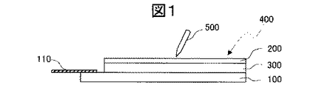
図1は、タッチパネル付き表示装置に組み込まれるタッチパネルの概略構成を示す断面図、
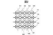
図2は、図1のタッチパネルの電極パターンを示す平面図、
図3は、図1の一部を拡大した断面図、
図4は、図1のタッチパネルの駆動回路を示すブロック図である。
図5は、タッチパネル付き表示装置の概略構成を示すブロック図である。
本実施例1のタッチパネル付き表示装置は、図5に示すように、液晶表示パネル600と、液晶液示パネル600の観察者側の面上に配置された静電容量結合方式のタッチパネル400と、液晶表示パネル600の観察者側とは反対側の面下に配置されたバックライト700とを備えている。液晶表示パネル600としては、例えばIPS方式、TN方式、VA方式等の液晶表示パネルが用いられている。
タッチパネル400は、図1に示すように、互いに対向して配置される第1及び第2の基板(100,200)と、第1の基板100と第2の基板200との間に挟持されるゲル状シート300と、第1の基板100の基板対向面(第2の基板200と対向する面)側の一辺側に一端側が固定されるフレキシブル配線基板(FPC)110とを有している。
Hereinafter, embodiments of the present invention will be described in detail with reference to the drawings. In all the drawings for explaining the embodiments of the invention, those having the same function are given the same reference numerals, and their repeated explanation is omitted.
[Example 1]
In the first embodiment, an example in which the present invention is applied to a display device with a capacitive coupling type touch panel provided with a touch panel on a liquid crystal display panel as an example of a display panel will be described.
1 to 5 are diagrams relating to a display device with a touch panel according to a first embodiment of the present invention.
FIG. 1 is a cross-sectional view illustrating a schematic configuration of a touch panel incorporated in a display device with a touch panel.
FIG. 2 is a plan view showing an electrode pattern of the touch panel of FIG.
3 is an enlarged cross-sectional view of a part of FIG.
FIG. 4 is a block diagram showing a drive circuit of the touch panel of FIG.
FIG. 5 is a block diagram illustrating a schematic configuration of a display device with a touch panel.
As shown in FIG. 5, the display device with a touch panel according to the first embodiment includes a liquid
As shown in FIG. 1, the
タッチパネル400は、図2に示すように、第1の方向(例えばY方向)に延在し、前記第1の方向と交差する第2の方向(例えばX方向)に所定の配列ピッチで並設される複数のX電極(X1〜X4)と、このX電極と交差して前記第2の方向に延在し、前記第1の方向に所定の配列ピッチで並設される複数のY電極(Y1〜Y4)とを有している。
X1〜X4のX電極は、タッチパネル領域10において、第1の部分と、この第1の部分の幅よりも広い幅の第2の部分122とが前記第1の方向(例えばY方向)に交互に複数配置された電極パターンで形成されている。
Y1〜Y4のY電極は、タッチパネル領域10において、第1の部分と、この第1の部分の幅よりも広い幅の第2の部分121とが前記第2の方向(例えばX方向)に交互に複数配置された電極パターンで形成されている。
X1〜X4のX電極の各々の第2の部分122は、平面的に見たとき、隣り合う2つのY電極間に配置されている。Y1〜Y4のY電極の各々の第2の部分121は、平面的に見たとき、隣り合う2つのX電極間に配置されている。X1〜X4のX電極の各々の第1の部分は、Y1〜Y4のY電極の各々の第1の部分と平面的に交差している。
As shown in FIG. 2, the
In the X electrodes X1 to X4, in the
In the Y electrodes Y1 to Y4, in the
The
第1の基板100は、X1〜X4のX電極とY1〜Y4のY電極とを有し、X1〜X4のX電極とY1〜Y4のY電極は、図3に示すように、第1の基板100の第2の基板200と対向する面側に絶縁膜120を介して積層されている。本実施例では、例えばY電極の方がX電極よりも上層に形成されている。
第2の基板200は、図3に示すように、第1の基板100と向かい合う面側に面状の対向電極201を有している。この対向電極201は、少なくともタッチパネル領域10の全てのX電極及びY電極を覆うようにして形成されている。
X電極(X1〜X4)及びY電極(Y1〜Y4)、並びに対向電極201は、例えばITO(Indium Tin Oxide)等の透明性導電材料で形成されている。
ゲル状シート300は、図3に示すように、第1の基板100のX電極及びY電極と、第2の基板200の対向電極201との間に設けられている。このゲル状シート300は、少なくともタッチパネル領域10の全てのX電極及びY電極を覆うようにして形成されている。本実施例において、ゲル状シート300は、これに限定されないが、例えば第2の基板200側に形成されている。
第1の基板100及び第2の基板200としては、透明な絶縁性基板が用いられている。本実施例では、第1及び第2の基板(100,200)としてガラス基板が用いられており、第2の基板200の厚さは第1の基板100の厚さよりも薄くなっている。
ゲル状シート300としては、例えばパラフィン系オイル、シリコーンゴム系の材料からなるものが用いられている。
The
As shown in FIG. 3, the
The X electrodes (X1 to X4), the Y electrodes (Y1 to Y4), and the
As illustrated in FIG. 3, the gel-
As the
As the gel-
図3では、対向電極201とX電極(X4),Y電極(Y3),X電極(X3)との間にC1,C2,C3の容量が形成されていることを模式的に示している。
このような構成にすることにより、図3に示すように、タッチパネル400のタッチ面(第2の基板200のタッチ面)を観察者がスタイラスペン500でタッチすると、第2の基板200が変形し、この変形に追従してゲル状シート300が変位(ゲル状シート300の厚さが変化)して、第1の基板100の電極(X電極又はY電極)と第2の基板200の対向電極201との間の容量が変化する。図3では、Y3のY電極上をスタイラスペン500でタッチしているため、Y3のY電極と対向電極201との間の容量が変化する。この容量変化を検出することで、スタイラスペンがタッチした位置を検出できる。
また、前述の容量変化はゲル状シート300の変位で生ずるので、観察者の指、先端が丸い棒状のものなどでもタッチ入力が可能である。
また、タッチの有無は容量の変化で検出するので、抵抗方式のように電極同士の接触がなく、信頼性の高いタッチパネル400を実現できる。
従って、指タッチ入力及びスタイラスペン入力が可能な信頼性の高い静電容量結合方式のタッチパネル付き表示装置を提供することができる。
なお、必要な容量変化を得るには、ゲル状シート300の硬度は2以上15以下が望ましい。
FIG. 3 schematically shows that capacitors C1, C2, and C3 are formed between the
With this configuration, as shown in FIG. 3, when the observer touches the touch surface of the touch panel 400 (the touch surface of the second substrate 200) with the
Further, since the above-described capacitance change is caused by the displacement of the gel-
In addition, since the presence or absence of a touch is detected by a change in capacitance, there is no contact between electrodes as in the resistance method, and a highly
Therefore, it is possible to provide a highly reliable capacitively coupled display device with a touch panel capable of finger touch input and stylus pen input.
In addition, in order to obtain a necessary capacity change, the hardness of the gel-
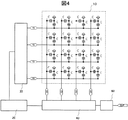
図4は、タッチパネルの駆動回路を示すブロック図である。図4において、10はタッチパネル領域(タッチセンサ領域)、20は制御回路、30はY駆動回路、40はX検出回路、60は座標検出回路である。また、X1〜X4は第1の方向(図1のY方向)に伸びるX電極、Y1〜Y4は第2の方向(図1のX方向)に伸びるY電極であり、CはX電極及びY電極と対向電極201とで形成される結合容量を示している。
図6は、図4に示すY駆動回路30を示す図である。
図6に示すように、Y駆動回路30は、シフトレジスタ310を有する。シフトレジスタ310の各シフト段の出力がHigh(以下、Hレベルという)となると、pMOSトランジスタ322がオフ、nMOSトランジスタ324がオンとなり、Y1〜Y4のY電極に基準電圧(ここでは、VLの電圧)が供給される。
また、シフトレジスタ310の各シフト段の出力がLow(以下、Lレベルという)となると、pMOSトランジスタ322がオン、nMOSトランジスタ324がオフとなり、Y1〜Y4のY電極に基準電圧より高電位の電圧(ここでは、VHの電圧)が供給される。
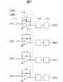
図7は、図4に示すX検出回路40を示す図である。
図7に示すように、X検出回路40は、オペアンプ412と積分容量418とで構成される積分回路を有する。積分回路の後段には、サンプルホールド回路422とA/D変換回路424が設けられる。
積分回路は、スイッチング素子414がオンのときに、Y1〜Y4のY電極に供給される電圧が、Hレベル→Lレベル、あるいは、Lレベル→Hレベルに変化したときに、X1〜X4に流れる電流を積分する。また、積分回路の積分容量418は、スイッチング素子416がオンの時にリセットされる。
FIG. 4 is a block diagram showing a touch panel drive circuit. In FIG. 4, 10 is a touch panel area (touch sensor area), 20 is a control circuit, 30 is a Y drive circuit, 40 is an X detection circuit, and 60 is a coordinate detection circuit. X1 to X4 are X electrodes extending in the first direction (Y direction in FIG. 1), Y1 to Y4 are Y electrodes extending in the second direction (X direction in FIG. 1), and C is the X electrode and Y The coupling capacitance formed by the electrode and the
FIG. 6 is a diagram showing the
As shown in FIG. 6, the
Further, when the output of each shift stage of the
FIG. 7 is a diagram showing the
As shown in FIG. 7, the
The integration circuit flows from X1 to X4 when the voltage supplied to the Y electrodes Y1 to Y4 changes from H level to L level or from L level to H level when the switching
図8は、図4に示すタッチパネルの動作を説明するためのタイミングチャートである。
Y駆動回路30のシフトレジスタ310には、スタートパルスSTと、クロックCLKとが入力され、Y1〜Y4のY電極に、順次Lレベルの電圧を供給する。
そして、Y1〜Y4のY電極の電圧が、Hレベル→Lレベルに変化した時と、Lレベル→Hレベルに変化した時に、Y1〜Y4のY電極からX1からX4のX電極にそれぞれ電流が流れる。
この電流を、X電極で検出する。例えば、Y1〜Y4のY電極からX1のX電極には、図8のI−11,I−21,I−31、I−41に示す電流が流れる。この結果、X1のX電極には、これらの電流和である図8のI−X1に示す電流が流れる。この電流を、積分回路で積分すると、図8のV−X1に示す電圧を検出することができる。なお、スイッチング素子414はタイミングパルスTG1によりオンとなり、スイッチング素子416はタイミングパルスTG2によりオンとなる。
本実施例において、X電極とY電極との結合容量が同じ場合には、Y1のY電極の電圧が、Lレベル→Hレベルに変化した時と、Y2のY電極がHレベル→Lレベルに変化した時に、X電極に流れる電流は、電流の向きが逆方向で、大きさが同じであるので、積分回路の出力電圧は、0となる。しかしながら、X電極とY電極との結合容量が異なる場合には、Y1のY電極の電圧が、Lレベル→Hレベルに変化した時と、Y2のY電極がHレベル→Lレベルに変化した時に、X電極に流れる電流は、電流の向きが逆方向で、大きさが容量差に応じて異なることになるので、積分回路の出力電圧は、0以外の電圧となる。
FIG. 8 is a timing chart for explaining the operation of the touch panel shown in FIG.
A start pulse ST and a clock CLK are input to the
When the voltage of the Y electrodes Y1 to Y4 changes from the H level to the L level, and when the voltage changes from the L level to the H level, current flows from the Y electrodes Y1 to Y4 to the X electrodes X1 to X4, respectively. Flowing.
This current is detected by the X electrode. For example, currents indicated by I-11, I-21, I-31, and I-41 in FIG. 8 flow from the Y electrodes Y1 to Y4 to the X electrode X1. As a result, the current indicated by I-X1 in FIG. 8 which is the sum of these currents flows through the X electrode of X1. When this current is integrated by an integration circuit, a voltage indicated by V-X1 in FIG. 8 can be detected. Note that the switching
In this embodiment, when the coupling capacitances of the X electrode and the Y electrode are the same, the voltage of the Y electrode of Y1 changes from L level to H level, and the Y electrode of Y2 changes from H level to L level. When the current changes, the current flowing through the X electrode has the opposite direction and the same magnitude, so the output voltage of the integrating circuit becomes zero. However, when the coupling capacities of the X electrode and the Y electrode are different, when the voltage of the Y electrode of Y1 changes from L level to H level, and when the Y electrode of Y2 changes from H level to L level The current flowing through the X electrode is in the opposite direction and the magnitude varies depending on the capacitance difference, so the output voltage of the integrating circuit is a voltage other than zero.
ここで、積分回路は、X電極で検出された電流値を積分するので、積分回路の出力電圧は、X電極とY電極との結合容量の容量差に比例することになる。
座標検出回路60は、Lレベルの電圧が供給されたY電極の位置と、各X電極で検出された電流値に応じて、観察者がスタイラスペン500でタッチした、タッチセンサ領域10のタッチ位置座標を検出する。この場合、本実施例では、観察者がタッチした複数のタッチ位置を検出することができる。
このように、本実施例では、X電極とY電極との結合容量の容量差を検出して、観察者がタッチしたタッチセンサ領域10の座標位置を検出するにしたので、X電極とY電極との間の寄生容量をキャンセルすることが可能である。
この結果、本実施例では、製造上生ずる配置上の変動によるX電極とY電極との間の寄生容量や、温度などの外的要因によるX電極とY電極との間の寄生容量の変動の影響を受けずに、観察者がスタイラスペン500でタッチした位置を検出することが可能となる。
一般に、観察者がスタイラスペン500でタッチセンサ領域10をタッチしたときの、X電極とY電極との結合容量は、X電極とY電極の電極数を増加すると減少するが、本実施例では、X電極とY電極との間の寄生容量をキャンセルして、より小さなX電極とY電極との結合容量を検出することができるので、より電極数が多い高分解のタッチパネルを実現することが可能となる。
Here, since the integration circuit integrates the current value detected by the X electrode, the output voltage of the integration circuit is proportional to the capacitance difference of the coupling capacitance between the X electrode and the Y electrode.
The coordinate
As described above, in this embodiment, since the capacitance difference of the coupling capacitance between the X electrode and the Y electrode is detected and the coordinate position of the
As a result, in the present embodiment, the parasitic capacitance between the X electrode and the Y electrode due to the variation in the layout that occurs in manufacturing, and the variation in the parasitic capacitance between the X electrode and the Y electrode due to external factors such as temperature. The position touched by the observer with the
In general, when the observer touches the
[実施例2]
図9は、本実施例2の液晶表示装置に使用されるタッチパネルの概略構成を示すブロック図である。
図9において、10はタッチセンサ領域、20は制御回路、70は電流検出回路、80は電極駆動回路である。
前述の実施例では、各Y電極に、時分割で順次Lレベルの電圧を供給し、各X電極に流れる電流を検出して座標位置を検出するようにしたが、本実施例では、制御回路20がスイッチ90を制御し、期間A内に、電極駆動回路80が、各Y電極に時分割で順次Lレベルの電圧を供給するとともに、電流検出回路70が、全X電極に流れる電流を検出し、また、期間B内に、電極駆動回路80が、各X電極に時分割で順次Lレベルの電圧を供給するとともに、電流検出回路70が、全Y電極に流れる電流を検出する。なお、電流検出回路70の後段には、座標検出回路が設けられるが、図9では省略している。
本実施例では、期間A内に、全X電極で検出される電流値は、連続する2つのY電極の一方と全X電極の間の結合容量と、連続する2つのY電極の他方と全X電極の間の結合容量との容量差に比例する。
したがって、期間A内に、観察者がスタイラスペン500でタッチしたタッチセンサ領域10のY電極の位置を検出することができ、同様に、期間B内に、全Y電極で検出された電流値に応じて、観察者がスタイラスペン500でタッチしたタッチセンサ領域10のX電極の位置を検出することができる。
これにより、観察者がタッチしたタッチセンサ領域10のタッチ位置座標を検出することができる。この場合、本実施例では、観察者がタッチした複数のタッチ位置を検出することができる。
[Example 2]
FIG. 9 is a block diagram illustrating a schematic configuration of a touch panel used in the liquid crystal display device according to the second embodiment.
In FIG. 9, 10 is a touch sensor region, 20 is a control circuit, 70 is a current detection circuit, and 80 is an electrode drive circuit.
In the above-described embodiment, the L level voltage is sequentially supplied to each Y electrode in a time division manner, and the current flowing through each X electrode is detected to detect the coordinate position. In this embodiment, however, the
In the present embodiment, during the period A, the current values detected by all the X electrodes are the coupling capacitance between one of the two consecutive Y electrodes and all the X electrodes, the other of the two consecutive Y electrodes, and the total. It is proportional to the capacitance difference with the coupling capacitance between the X electrodes.
Therefore, the position of the Y electrode in the
Thereby, the touch position coordinate of the touch sensor area |
図10は、図9に示す電極駆動回路80の一例を示す図である。
図10において、810はシフトレジスタ、822はpMOSトランジスタ、824はnMOSトランジスタである。図10において、太線はバス接続であることを示しており、図10に示す電極駆動回路80の回路構成は、図6に示すY駆動回路30と同じである。
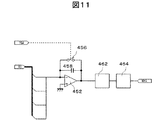
図11は、図9に示す電流検出回路70の一例を示す図である。図11においても、太線はバス接続であることを示している。
図11に示す構成では、電流検出回路70において、オペアンプ452と積分容量458とで構成される積分回路は、全電極(X電極、あるいは、Y電極)に流れる電流を積分する。なお、スイッチング素子456はタイミングパルスTG1によりオンとなり、スイッチング素子456がオンの時に積分容量はリセットされる。なお、図11において、462はサンプルホールド回路、464はA/D変換回路である。
FIG. 10 is a diagram illustrating an example of the
In FIG. 10, 810 is a shift register, 822 is a pMOS transistor, and 824 is an nMOS transistor. In FIG. 10, a thick line indicates a bus connection, and the circuit configuration of the
FIG. 11 is a diagram illustrating an example of the
In the configuration shown in FIG. 11, in the
[実施例3]
図12乃至図14は、本発明の実施例3のタッチパネル付き表示装置に係る図であり、
図12は、タッチパネル付き表示装置に組み込まれるタッチパネルの概略構成を示す断面図、
図13は、図12のタッチパネルの電極パターンを示す平面図、
図14は、図12の一部を拡大した断面図である。
本実施例2のタッチパネル付き表示装置は、基本的に前述の実施例1と同様の構成になっており、タッチパネルの構成が異なっている。
前記の実施例1のタッチパネル400は、図3に示すように、第1の基板100側にX電極(X1〜X4)及びY電極(Y1〜Y4)が形成され、第2の基板200側に対向電極201が形成された構成になっている。これに対し、本実施例2のタッチパネル401は、図14に示すように、第1の基板100側にY電極(Y1〜Y4)が形成され、第2の基板200側にX電極(X1〜X4)が形成された構成になっている。以下、本実施例2のタッチパネル401について説明する。
[Example 3]
12 to 14 are diagrams related to a display device with a touch panel according to a third embodiment of the present invention.
FIG. 12 is a cross-sectional view illustrating a schematic configuration of a touch panel incorporated in a display device with a touch panel.
FIG. 13 is a plan view showing an electrode pattern of the touch panel of FIG.
FIG. 14 is an enlarged cross-sectional view of a part of FIG.
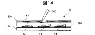
The display device with a touch panel of the second embodiment has basically the same configuration as that of the first embodiment described above, and the configuration of the touch panel is different.
As shown in FIG. 3, the
タッチパネル401は、図12に示すように、互いに対向して配置される第1及び第2の基板(100,200)と、第1の基板100と第2の基板200との間に挟持されるゲル状シート300と、第1の基板100の基板対向面(第2の基板200と対向する面)側の一辺側に一端側が固定されるフレキシブル配線基板(FPC)111と、第2の基板200の基板対向面(第1の基板100と対向する面)側の一辺側に一端側が固定されるフレキシブル配線基板(FPC)112とを有している。また、タッチパネル401は、図2に示すタッチパネル領域(タッチセンサ領域)10を有している。
タッチパネル401は、図13に示すように、第1の方向(例えばY方向)に所定の一定幅で延在し、前記第1の方向と交差する第2の方向(例えばX方向)に所定の配列ピッチで並設される複数のX電極(X1〜X4)と、このX電極と交差して前記第2の方向に所定の一定幅で延在し、前記第1の方向に所定の配列ピッチで並設される複数のY電極(Y1〜Y4)とを有している。Y電極(Y1〜Y4)及びX電極(X1〜X4)は、タッチパネル領域10の内外に亘って延在している。
As shown in FIG. 12, the
As shown in FIG. 13, the
図14に示すように、第1の基板100は、Y電極(Y1〜Y4)を有し、Y電極(Y1〜Y4)は、第1の基板100の第2の基板200と対向する面側に形成されている。第2の基板200は、X電極(X1〜X4)を有し、X電極(X1〜X4)は、第2の基板200の第1の基板100と対向する面側に形成されている。
Y電極(Y1〜Y4)とX電極(X1〜X4)は、これらの間にゲル状シート300を介して積層されており、ゲル状シート300は、少なくともタッチパネル領域内の全てのY電極及びX電極を覆うようにして形成されている。ゲル状シート300は、これに限定されないが、本実施例2においても、例えば第2の基板200側に形成されている。
本実施例のタッチパネル401は、第1及び第2の基板(100,200)の何れにも、実施例1の対向電極201が設けられていない。
X電極(X1〜X4)及びY電極(Y1〜Y4)は、例えばITO(Indium Tin Oxide)等の透明性導電材料で形成されている。
第1の基板100及び第2の基板200としては、透明な絶縁性基板が用いられている。本実施例では、第1及び第2の基板(100,200)としてガラス基板が用いられており、第2の基板200の厚さは第1の基板100の厚さよりも薄くなっている。
ゲル状シート300としては、例えばパラフィン系オイル、シリコーンゴム系の材料からなるものが用いられている。
As shown in FIG. 14, the
The Y electrode (Y1 to Y4) and the X electrode (X1 to X4) are laminated via a gel-
In the
The X electrodes (X1 to X4) and the Y electrodes (Y1 to Y4) are made of a transparent conductive material such as ITO (Indium Tin Oxide).
As the
As the gel-
図14では、X電極(X3)とY電極(X2),(Y3),(Y4)との間にC1,C2,C3の容量が形成されていることを模式的に示している。
図14に示すように、タッチパネル401のタッチ面(第2の基板200のタッチ面)を観察者がスタイラスペン500でタッチすると、第2の基板200が変形し、この変形に追従してゲル状シート300が変位(ゲル状シート300の厚さが変化)して、第1の基板100のY電極と第2の基板200のX電極との間の容量が変化する。図14では、Y3のY電極上及びX3のX電極上をスタイラスペン500でタッチしているため、Y3のY電極とX3のX電極との間の容量が変化する。この容量変化を検出することで、前述の実施例1と同様に、スタイラスペンがタッチした位置を検出できる。
また、前述の容量変化はゲル状シート300の変位で生ずるので、観察者の指、先端が丸い棒状のものなどでもタッチ入力が可能である。
また、タッチの有無は容量の変化で検出するので、抵抗方式のように電極同士の接触がなく、信頼性の高いタッチパネル401を実現できる。
従って、本実施例2においても、指タッチ入力及びスタイラスペン入力が可能な信頼性の高い静電容量結合方式のタッチパネル付き表示装置を提供することができる。
また、ゲル状シート300の屈折率を第1及び第2の基板とほぼ等しくすることで、第1及び第2の基板の各々の電極パターンを見え難くすることができる。
FIG. 14 schematically shows that capacitors C1, C2, and C3 are formed between the X electrode (X3) and the Y electrodes (X2), (Y3), and (Y4).
As shown in FIG. 14, when an observer touches the touch surface of the touch panel 401 (the touch surface of the second substrate 200) with the
Further, since the above-described capacitance change is caused by the displacement of the gel-
Further, since the presence or absence of a touch is detected by a change in capacitance, there is no contact between electrodes as in the resistance method, and a highly
Therefore, also in the second embodiment, a highly reliable capacitively coupled display device with a touch panel capable of finger touch input and stylus pen input can be provided.
Moreover, by making the refractive index of the gel-
図15は、本実施例3のタッチパネルの概略構成を示すブロック図である。
図15において、10はタッチセンサ領域、210はY電極選択回路、220はX電極選択回路、230は電流検出回路である。Y電極選択回路210と、X電極選択回路220とは同一の回路構成を有するが、図15では、Y電極選択回路210の回路構成のみを図示している。
Y電極選択回路210およびX電極選択回路220は、走査回路211と、走査回路212とを有する。走査回路212は、期間A内に全スイッチング素子SW3をオフ、期間B内に、全スイッチング素子SW3をオンとする。
走査回路211は、期間A内に、時分割で順次、隣接する電極(Y電極、あるいはX電極)に対応するスイッチング素子SW1とスイッチング素子SW2のオン・オフを制御し、期間B内に、全スイッチング素子SW1と全スイッチング素子SW2とをオフとする。例えば、走査回路211は、期間Aの始めの時分割期間に、スイッチング素子SW1−1をオン、スイッチング素子SW2−1をオンとし、さらに、残りのスイッチング素子SW1とスイッチング素子SW2とをオフにする。
また、次の時分割期間に、スイッチング素子SW1−2をオン、スイッチング素子SW2−2をオンとし、さらに、残りのスイッチング素子SW1とスイッチング素子SW2とをオフにする。以下、同様にして、電極(Y電極、あるいはX電極)を選択する。
FIG. 15 is a block diagram illustrating a schematic configuration of the touch panel according to the third embodiment.
In FIG. 15, 10 is a touch sensor region, 210 is a Y electrode selection circuit, 220 is an X electrode selection circuit, and 230 is a current detection circuit. Although the Y
The Y
The
In the next time division period, the switching element SW1-2 is turned on, the switching element SW2-2 is turned on, and the remaining switching elements SW1 and SW2 are turned off. Hereinafter, similarly, an electrode (Y electrode or X electrode) is selected.
図16は、図15に示す電流検出回路230の一例を示す図である。
図16において、221はオペアンプ、222は積分容量、223はスイッチ制御回路、224はサンプルホールド回路、225はA/D変換回路である。なお、図16において、T1、T2は、X電極あるいはY電極の隣接する2つの電極を示す。
図17は、図16の電流検出回路230の動作を説明するためのタイムチャートである。
以下、図16のT1、T2に、Y1とY2の電極が接続されているもの(以下、仮定A)として、図16に示す電流検出回路の動作を説明する。
前述した仮定Aの場合に、Y電極選択回路210内のスイッチング素子SW1−1はオン、スイッチング素子SW2−1はオン、残りのスイッチング素子SW1とスイッチング素子SW2とはオフ、かつ、全スイッチ素子SW3はオフとなっている。
また、X電極選択回路220内の全スイッチング素子SW1と全スイッチング素子SW2はオフ、全スイッチング素子SW3はオンとなり、全X電極には基準電圧(GND)が供給される。
図17に示すように、始めに、スイッチ制御回路223の制御下に、スイッチング素子SW_Aがオンとなり、積分容量222がリセットされる。次に、スイッチ制御回路223の制御下に、スイッチング素子SW_Bがオンとなり、Y1の電極に、電圧レベルが基準電圧(GND)よりも高電位(+Vref)の正極性のパルスが、Y2の電極に、電圧レベルが基準電圧(GND)よりも低電位(−Vref)の負極性のパルスを供給される。その後、スイッチ制御回路223の制御下に、スイッチング素子SW_Cがオンとなり、オペアンプ221と積分容量222とから構成される積分回路からVoの電圧が得られる。
FIG. 16 shows an example of
In FIG. 16, 221 is an operational amplifier, 222 is an integration capacitor, 223 is a switch control circuit, 224 is a sample hold circuit, and 225 is an A / D conversion circuit. In FIG. 16, T1 and T2 indicate two electrodes adjacent to the X electrode or the Y electrode.
FIG. 17 is a time chart for explaining the operation of the
The operation of the current detection circuit shown in FIG. 16 will be described below assuming that the electrodes Y1 and Y2 are connected to T1 and T2 in FIG. 16 (hereinafter assumed A).
In the case of Assumption A described above, the switching element SW1-1 in the Y
In addition, all the switching elements SW1 and all the switching elements SW2 in the X
As shown in FIG. 17, first, under the control of the
ここで、Voは、下記(1)式で表される。
[数1]
Vo=Vref/Co×(Cn+1−Cn) ・・・・・・・・・・・ (1)
但し、Coは、積分容量222の容量値、Cnは、隣接する2つのY電極の中の一方の電極(ここでは、Y1の電極)と全X電極との間の結合容量、Cn+1は、隣接する2つの電極の中の他方の電極(ここでは、Y2の電極)と全X電極との間の結合容量である。なお、図16のT1、T2に、X電極の中の隣接する2つの電極が接続されている場合には、Cnは、隣接する2つのX電極の中の一方の電極と全Y電極との間の結合容量、Cn+1は、隣接する2つのX電極の中の他方の電極と全Y電極との間の結合容量となる。
このように、全X電極で検出される電流値は、連続する2つのY電極の一方と全X電極の間の結合容量と、連続する2つのY電極の他方と全X電極の間の結合容量との容量差に比例する。
したがって、期間A内に、全X電極に基準電圧(GND)を供給するとともに、Y電極を時分割で順次Y電極の中の隣接する2つの電極を選択し、一方の電極に正極性のパルスを、他方の電極に負極性のパルスを供給することにより、観察者がスタイラスペン500でタッチしたタッチセンサ領域10のY電極の位置を検出することが可能となる。
同様に、期間B内に、全Y電極に基準電圧(GND)を供給するとともに、X電極を時分割で順次X電極の中の隣接する2つの電極を選択し、一方の電極に正極性のパルスを、他方の電極に負極性のパルスを供給することにより、観察者がスタイラスペン500でタッチしたタッチセンサ領域10のX電極の位置を検出することが可能となる。
これにより、観察者がタッチしたタッチセンサ領域10のタッチ位置座標を検出することができる。この場合、本実施例では、観察者がタッチした複数のタッチ位置を検出することができる。
Here, Vo is expressed by the following equation (1).
[Equation 1]
Vo = Vref / Co × (Cn + 1−Cn) (1)
Where Co is the capacitance value of the integrating
Thus, the current value detected by all X electrodes is the coupling capacity between one of the two consecutive Y electrodes and all the X electrodes, and the coupling between the other of the two consecutive Y electrodes and all the X electrodes. It is proportional to the capacity difference from the capacity.
Therefore, within the period A, the reference voltage (GND) is supplied to all the X electrodes, the Y electrodes are sequentially selected in time-division manner, and two adjacent electrodes among the Y electrodes are selected, and a positive pulse is applied to one electrode. By supplying a negative pulse to the other electrode, it is possible to detect the position of the Y electrode in the
Similarly, within the period B, the reference voltage (GND) is supplied to all the Y electrodes, the X electrodes are sequentially selected in time division, and two adjacent electrodes among the X electrodes are selected, and one electrode has a positive polarity. By supplying a negative pulse to the other electrode, the position of the X electrode in the
Thereby, the touch position coordinate of the touch sensor area |
なお、本実施例3のタッチパネルの駆動方法として、前述の実施例1の駆動方法を採用してもよく、同様に、本実施例3のタッチパネルの駆動方法として、前述の実施例2の駆動方法を採用してもよい。
また、前述の実施例1及び実施例3では、第1及び第2の基板(100,200)としてガラス基板を用いた例について説明したが、第1及び第2の基板(100,200)として、例えば、絶縁性樹脂からなるプラスチック基板を用いてもよく、或いは第1の基板100として、例えば、ガラス基板、第2基板200としてプラスチック基板を用いてもよい。
また、前述の実施例1及び実施例3では、第2の基板200側にゲル状シート300を設けた例について説明したが、ゲル状シート300は第1の基板100側に設けてもよい。
さらに、前述までの説明では、本発明を液晶表示装置に適用した実施例について説明したが、本発明はこれに限定されるものではなく、例えば、有機EL表示装置などの表示装置全般にも適用可能である。
以上、本発明者によってなされた発明を、前記実施例に基づき具体的に説明したが、本発明は、前記実施例に限定されるものではなく、その要旨を逸脱しない範囲において種々変更可能であることは勿論である。
As the touch panel driving method according to the third embodiment, the driving method according to the first embodiment may be adopted. Similarly, as the touch panel driving method according to the third embodiment, the driving method according to the second embodiment described above. May be adopted.
In the first and third embodiments described above, the example in which the glass substrate is used as the first and second substrates (100, 200) has been described. However, as the first and second substrates (100, 200), For example, a plastic substrate made of an insulating resin may be used, or a glass substrate may be used as the
In the first and third embodiments, the example in which the gel-
Further, in the above description, the embodiment in which the present invention is applied to the liquid crystal display device has been described. However, the present invention is not limited to this, and for example, the present invention is also applicable to display devices such as organic EL display devices in general. Is possible.
As mentioned above, the invention made by the present inventor has been specifically described based on the above embodiments. However, the present invention is not limited to the above embodiments, and various modifications can be made without departing from the scope of the invention. Of course.
10 タッチパネル領域(タッチセンサ領域)
20 制御回路
30 Y駆動回路
40 X検出回路
50 容量検出回路
60 座標検出回路
70,230 電流検出回路
80 電極駆動回路
90 スイッチ
100 第1の基板
110,111,112 フレキシブル配線基板
120 絶縁膜
121,122 第2の部分
200 第2の基板
201 対向電極
210 Y電極選択回路
220 X電極選択回路
211,212 走査回路
221,412,452 オペアンプ
222,418,458 積分容量
223 スイッチ制御回路
224,422,462 サンプルホールド回路
225,424,464 A/D変換回路
300 ゲル状シート
310,440,810 シフトレジスタ
322,822 pMOSトランジスタ
324,824 nMOSトランジスタ
400,401 タッチパネル
414,416,441〜444,456,SW1〜SW6,SW_A,SW_B,SW_C スイッチング素子
500 スタイラスペン
600 液晶表示パネル
700 バックライト
X1〜X4 X電極
Y1〜Y4 Y電極
10 Touch panel area (touch sensor area)
DESCRIPTION OF
Claims (18)
前記表示パネルの観察者側の面上に配置される静電容量結合方式のタッチパネルとを備えた表示装置であって、
前記タッチパネルは、互いに対向して配置される第1及び第2の基板を有し、
前記第1の基板は、前記第2の基板と対向する面側に、第1の方向に延在し、前記第1の方向と交差する第2の方向に並設される複数の第1の電極と、
前記第1の電極と交差して前記第2の方向に延在し、前記第1の方向に並設される複数の第2の電極とを有し、
前記第2の基板は、前記第1の基板と対向する面側に、前記複数の第1及び第2の電極を覆う面状の第3の電極を有し、
前記複数の第1及び第2の電極と前記第3の電極との間には、ゲル状シートが設けられていることを特徴とする表示装置。 A display panel;
A display device comprising a capacitively coupled touch panel disposed on a viewer side surface of the display panel,
The touch panel includes first and second substrates disposed to face each other,
The first substrate extends in a first direction on a surface facing the second substrate, and is arranged in parallel in a second direction intersecting the first direction. Electrodes,
A plurality of second electrodes extending in the second direction intersecting the first electrode and arranged in parallel in the first direction;
The second substrate has a planar third electrode that covers the plurality of first and second electrodes on the surface facing the first substrate,
A display device, wherein a gel-like sheet is provided between the plurality of first and second electrodes and the third electrode.
前記第2の基板の厚さは前記第1の基板の厚さよりも薄いことを特徴とする請求項1に記載の表示装置。 The first and second substrates are glass substrates;
The display device according to claim 1, wherein a thickness of the second substrate is thinner than a thickness of the first substrate.
前記第2の基板はプラスチック基板であることを特徴とする請求項1に記載の表示装置。 The first substrate is a glass substrate;
The display device according to claim 1, wherein the second substrate is a plastic substrate.
検出回路と、
前記タッチパネルへのタッチ位置を演算する座標位置演算回路とを有し、
前記駆動回路は、前記複数の第1の電極の中から2つの第1の電極を順次選択し、当該選択された2つの第1の電極の一方に基準電圧よりも高電位の電圧を、他方に基準電圧を供給し、
前記検出回路は、選択した前記第2の電極と前記高電位の電圧が供給された前記第1の電極との間の容量Aと、前記選択した前記第2の電極と前記基準電圧が供給された前記第1の電極との間の容量Bとの間の容量差(A−B)を検出し、
前記座標位置演算回路は、前記選択された第1の電極および第2の電極の位置と、前記容量差(A−B)に基づき前記タッチパネルへのタッチ位置を演算することを特徴とする請求項1に記載のタッチパネル付き表示装置。 A drive circuit;
A detection circuit;
A coordinate position calculation circuit for calculating a touch position on the touch panel,
The drive circuit sequentially selects two first electrodes from the plurality of first electrodes, and applies a voltage higher than a reference voltage to one of the two selected first electrodes, Supply a reference voltage to
The detection circuit is supplied with a capacitor A between the selected second electrode and the first electrode to which the high potential voltage is supplied, and the selected second electrode and the reference voltage. A capacitance difference (A−B) between the first electrode and the capacitance B between the first electrode and the first electrode;
The coordinate position calculation circuit calculates a touch position on the touch panel based on the positions of the selected first electrode and second electrode and the capacitance difference (A−B). A display device with a touch panel according to 1.
検出回路と、
前記タッチパネルへのタッチ位置を演算する座標位置演算回路とを有し、
前記駆動回路は、期間Aに前記複数の第1の電極の中から2つの第1の電極を順次選択し、当該選択された2つの第1の電極の一方に基準電圧よりも高電位の電圧を、他方に基準電圧を供給するとともに、期間Bに前記複数の第2の電極の中から2つの第2の電極を順次選択し、当該選択された2つの第2の電極の一方に基準電圧よりも高電位の電圧を、他方に基準電圧を供給し、
前記検出回路は、前記期間Aに前記各第2の電極と前記高電位の電圧が供給された前記第1の電極との間の容量Aと、前記各第2の電極と前記基準電圧が供給された前記第1の電極との間の容量Bとの間の容量差(A−B)を検出し、前記期間Bに前記各第1の電極と前記高電位の電圧が供給された前記第2の電極との間の容量Cと、前記各第1の電極と前記基準電圧が供給された前記第2の電極との間の容量Dとの間の容量差(C−D)を検出し、
前記座標位置演算回路は、前記選択された第1の電極および前記容量差(A−B)と、前記選択された第2の電極および前記容量差(C−D)とに基づき前記タッチパネルへのタッチ位置を演算することを特徴とする請求項1に記載のタッチパネル付き表示装置。 A drive circuit;
A detection circuit;
A coordinate position calculation circuit for calculating a touch position on the touch panel,
The drive circuit sequentially selects two first electrodes from the plurality of first electrodes in a period A, and applies a voltage higher than a reference voltage to one of the selected two first electrodes. , A reference voltage is supplied to the other, and two second electrodes are sequentially selected from the plurality of second electrodes in period B, and a reference voltage is applied to one of the two selected second electrodes. A higher potential voltage and a reference voltage to the other,
The detection circuit is supplied with a capacitor A between each second electrode and the first electrode to which the high potential voltage is supplied in the period A, and each second electrode and the reference voltage. The capacitance difference (A−B) between the first electrode and the capacitor B is detected, and the first electrode and the high potential voltage are supplied in the period B. A capacitance difference (C−D) between the capacitance C between the two electrodes and the capacitance D between each of the first electrodes and the second electrode supplied with the reference voltage. ,
The coordinate position calculation circuit outputs the touch panel to the touch panel based on the selected first electrode and the capacitance difference (A−B) and the selected second electrode and the capacitance difference (C−D). The display device with a touch panel according to claim 1, wherein a touch position is calculated.
第2電極選択回路と、
検出回路と、
前記タッチパネルへのタッチ位置を演算する座標位置演算回路とを有し、
前記第1電極選択回路は、期間Aに前記複数の第1の電極の中から2つの第1の電極を順次選択し、当該選択された2つの第1の電極の一方に電圧レベルが基準電圧よりも高電位の正極性のパルスを、他方に電圧レベルが基準電圧よりも低電位の負極性のパルスを供給し、
前記第2電極選択回路は、期間Bに前記複数の第2の電極の中から2つの第2の電極を順次選択し、当該選択された2つの第2の電極の一方に電圧レベルが基準電圧よりも高電位の正極性のパルスを、他方に電圧レベルが基準電圧よりも低電位の負極性のパルスを供給し、
前記検出回路は、前記期間Aに前記各第2の電極と前記正極性のパルスが供給された前記第1の電極との間の容量Aと、前記各第2の電極と前記負極性のパルスが供給された前記第1の電極との間の容量Bとの間の容量差(A−B)を検出し、前記期間Bに前記各第1の電極と前記正極性のパルスが供給された前記第2の電極との間の容量Cと、前記各第1の電極と前記負極性のパルスが供給された前記第2の電極との間の容量Dとの間の容量差(C−D)を検出し、
前記座標位置演算回路は、前記選択された第1の電極および前記容量差(A−B)と、前記選択された第2の電極および前記容量差(C−D)とに基づき前記タッチパネルへのタッチ位置を演算することを特徴とする請求項1に記載のタッチパネル付き表示装置。 A first electrode selection circuit;
A second electrode selection circuit;
A detection circuit;
A coordinate position calculation circuit for calculating a touch position on the touch panel,
The first electrode selection circuit sequentially selects two first electrodes from the plurality of first electrodes in period A, and a voltage level is applied to one of the two selected first electrodes as a reference voltage. A positive polarity pulse with a higher potential than the negative voltage pulse with a voltage level lower than the reference voltage on the other side,
The second electrode selection circuit sequentially selects two second electrodes from the plurality of second electrodes in period B, and a voltage level is applied to one of the two selected second electrodes as a reference voltage. A positive polarity pulse with a higher potential than the negative voltage pulse with a voltage level lower than the reference voltage on the other side,
The detection circuit includes a capacitance A between each second electrode and the first electrode to which the positive pulse is supplied during the period A, and each second electrode and the negative pulse. A capacitance difference (A−B) between the first electrode and the capacitor B is detected, and the first electrode and the positive pulse are supplied in the period B. A capacitance difference (C−D) between the capacitance C between the second electrode and the capacitance D between each first electrode and the second electrode supplied with the negative pulse. )
The coordinate position calculation circuit outputs the touch panel to the touch panel based on the selected first electrode and the capacitance difference (A−B) and the selected second electrode and the capacitance difference (C−D). The display device with a touch panel according to claim 1, wherein a touch position is calculated.
前記表示パネルの観察者側の面上に配置される静電容量結合方式のタッチパネルとを備えた表示装置であって、
前記タッチパネルは、互いに対向して配置される第1及び第2の基板を有し、
前記第1の基板は、前記第2の基板と対向する面側に、第1の方向に延在し、前記第1の方向と交差する第2の方向に並設される複数の第1の電極を有し、
前記第2の基板は、前記第1の基板と対向する面側に、前記第1の電極と交差して前記第2の方向に延在し、前記第1の方向に並設される複数の第2の電極を有し、
前記複数の第1の電極と前記複数の第2の電極との間には、ゲル状シートが設けられていることを特徴とする表示装置。 A display panel;
A display device comprising a capacitively coupled touch panel disposed on a viewer side surface of the display panel,
The touch panel includes first and second substrates disposed to face each other,
The first substrate extends in a first direction on a surface facing the second substrate, and is arranged in parallel in a second direction intersecting the first direction. Having electrodes,
The second substrate extends on the surface facing the first substrate, intersects the first electrode, extends in the second direction, and is arranged in parallel in the first direction. Having a second electrode;
A display device, wherein a gel-like sheet is provided between the plurality of first electrodes and the plurality of second electrodes.
前記第2の基板の厚さは前記第1の基板の厚さよりも薄いことを特徴とする請求項10に記載の表示装置。 The first and second substrates are glass substrates;
The display device according to claim 10, wherein a thickness of the second substrate is thinner than a thickness of the first substrate.
前記第2の基板はプラスチック基板であることを特徴とする請求項10に記載の表示装置。 The first substrate is a glass substrate;
The display device according to claim 10, wherein the second substrate is a plastic substrate.
検出回路と、
前記タッチパネルへのタッチ位置を演算する座標位置演算回路とを有し、
前記駆動回路は、前記複数の第1の電極の中から2つの第1の電極を順次選択し、当該選択された2つの第1の電極の一方に基準電圧よりも高電位の電圧を、他方に基準電圧を供給し、
前記検出回路は、選択した前記第2の電極と前記高電位の電圧が供給された前記第1の電極との間の容量Aと、前記選択した前記第2の電極と前記基準電圧が供給された前記第1の電極との間の容量Bとの間の容量差(A−B)を検出し、
前記座標位置演算回路は、前記選択された第1の電極および第2の電極の位置と、前記容量差(A−B)に基づき前記タッチパネルへのタッチ位置を演算することを特徴とする請求項10に記載のタッチパネル付き表示装置。 A drive circuit;
A detection circuit;
A coordinate position calculation circuit for calculating a touch position on the touch panel,
The drive circuit sequentially selects two first electrodes from the plurality of first electrodes, and applies a voltage higher than a reference voltage to one of the two selected first electrodes, Supply a reference voltage to
The detection circuit is supplied with a capacitor A between the selected second electrode and the first electrode to which the high potential voltage is supplied, and the selected second electrode and the reference voltage. A capacitance difference (A−B) between the first electrode and the capacitance B between the first electrode and the first electrode;
The coordinate position calculation circuit calculates a touch position on the touch panel based on the positions of the selected first electrode and second electrode and the capacitance difference (A−B). 10. A display device with a touch panel according to 10.
検出回路と、
前記タッチパネルへのタッチ位置を演算する座標位置演算回路とを有し、
前記駆動回路は、期間Aに前記複数の第1の電極の中から2つの第1の電極を順次選択し、当該選択された2つの第1の電極の一方に基準電圧よりも高電位の電圧を、他方に基準電圧を供給するとともに、期間Bに前記複数の第2の電極の中から2つの第2の電極を順次選択し、当該選択された2つの第2の電極の一方に基準電圧よりも高電位の電圧を、他方に基準電圧を供給し、
前記検出回路は、前記期間Aに前記各第2の電極と前記高電位の電圧が供給された前記第1の電極との間の容量Aと、前記各第2の電極と前記基準電圧が供給された前記第1の電極との間の容量Bとの間の容量差(A−B)を検出し、前記期間Bに前記各第1の電極と前記高電位の電圧が供給された前記第2の電極との間の容量Cと、前記各第1の電極と前記基準電圧が供給された前記第2の電極との間の容量Dとの間の容量差(C−D)を検出し、
前記座標位置演算回路は、前記選択された第1の電極および前記容量差(A−B)と、前記選択された第2の電極および前記容量差(C−D)とに基づき前記タッチパネルへのタッチ位置を演算することを特徴とする請求項10に記載のタッチパネル付き表示装置。 A drive circuit;
A detection circuit;
A coordinate position calculation circuit for calculating a touch position on the touch panel,
The drive circuit sequentially selects two first electrodes from the plurality of first electrodes in a period A, and applies a voltage higher than a reference voltage to one of the selected two first electrodes. , A reference voltage is supplied to the other, and two second electrodes are sequentially selected from the plurality of second electrodes in period B, and a reference voltage is applied to one of the two selected second electrodes. A higher potential voltage and a reference voltage to the other,
The detection circuit is supplied with a capacitor A between each second electrode and the first electrode to which the high potential voltage is supplied in the period A, and each second electrode and the reference voltage. The capacitance difference (A−B) between the first electrode and the capacitor B is detected, and the first electrode and the high potential voltage are supplied in the period B. A capacitance difference (C−D) between the capacitance C between the two electrodes and the capacitance D between each of the first electrodes and the second electrode supplied with the reference voltage. ,
The coordinate position calculation circuit outputs the touch panel to the touch panel based on the selected first electrode and the capacitance difference (A−B) and the selected second electrode and the capacitance difference (C−D). The display device with a touch panel according to claim 10, wherein a touch position is calculated.
第2電極選択回路と、
検出回路と、
前記タッチパネルへのタッチ位置を演算する座標位置演算回路とを有し、
前記第1電極選択回路は、期間Aに前記複数の第1の電極の中から2つの第1の電極を順次選択し、当該選択された2つの第1の電極の一方に電圧レベルが基準電圧よりも高電位の正極性のパルスを、他方に電圧レベルが基準電圧よりも低電位の負極性のパルスを供給し、
前記第2電極選択回路は、期間Bに前記複数の第2の電極の中から2つの第2の電極を順次選択し、当該選択された2つの第2の電極の一方に電圧レベルが基準電圧よりも高電位の正極性のパルスを、他方に電圧レベルが基準電圧よりも低電位の負極性のパルスを供給し、
前記検出回路は、前記期間Aに前記各第2の電極と前記正極性のパルスが供給された前記第1の電極との間の容量Aと、前記各第2の電極と前記負極性のパルスが供給された前記第1の電極との間の容量Bとの間の容量差(A−B)を検出し、前記期間Bに前記各第1の電極と前記正極性のパルスが供給された前記第2の電極との間の容量Cと、前記各第1の電極と前記負極性のパルスが供給された前記第2の電極との間の容量Dとの間の容量差(C−D)を検出し、
前記座標位置演算回路は、前記選択された第1の電極および前記容量差(A−B)と、前記選択された第2の電極および前記容量差(C−D)とに基づき前記タッチパネルへのタッチ位置を演算することを特徴とする請求項10に記載のタッチパネル付き表示装置。 A first electrode selection circuit;
A second electrode selection circuit;
A detection circuit;
A coordinate position calculation circuit for calculating a touch position on the touch panel,
The first electrode selection circuit sequentially selects two first electrodes from the plurality of first electrodes in period A, and a voltage level is applied to one of the two selected first electrodes as a reference voltage. A positive polarity pulse with a higher potential than the negative voltage pulse with a voltage level lower than the reference voltage on the other side,
The second electrode selection circuit sequentially selects two second electrodes from the plurality of second electrodes in period B, and a voltage level is applied to one of the two selected second electrodes as a reference voltage. A positive polarity pulse with a higher potential than the negative voltage pulse with a voltage level lower than the reference voltage on the other side,
The detection circuit includes a capacitance A between each second electrode and the first electrode to which the positive pulse is supplied during the period A, and each second electrode and the negative pulse. A capacitance difference (A−B) between the first electrode and the capacitor B is detected, and the first electrode and the positive pulse are supplied in the period B. A capacitance difference (C−D) between the capacitance C between the second electrode and the capacitance D between each first electrode and the second electrode supplied with the negative pulse. )
The coordinate position calculation circuit outputs the touch panel to the touch panel based on the selected first electrode and the capacitance difference (A−B) and the selected second electrode and the capacitance difference (C−D). The display device with a touch panel according to claim 10, wherein a touch position is calculated.
Priority Applications (2)
| Application Number | Priority Date | Filing Date | Title |
|---|---|---|---|
| JP2008160272A JP5133791B2 (en) | 2008-06-19 | 2008-06-19 | Display device with touch panel |
| US12/486,003 US20090315858A1 (en) | 2008-06-19 | 2009-06-17 | Display Device with Touch Panel |
Applications Claiming Priority (1)
| Application Number | Priority Date | Filing Date | Title |
|---|---|---|---|
| JP2008160272A JP5133791B2 (en) | 2008-06-19 | 2008-06-19 | Display device with touch panel |
Publications (2)
| Publication Number | Publication Date |
|---|---|
| JP2010003048A true JP2010003048A (en) | 2010-01-07 |
| JP5133791B2 JP5133791B2 (en) | 2013-01-30 |
Family
ID=41430731
Family Applications (1)
| Application Number | Title | Priority Date | Filing Date |
|---|---|---|---|
| JP2008160272A Active JP5133791B2 (en) | 2008-06-19 | 2008-06-19 | Display device with touch panel |
Country Status (2)
| Country | Link |
|---|---|
| US (1) | US20090315858A1 (en) |
| JP (1) | JP5133791B2 (en) |
Cited By (25)
| Publication number | Priority date | Publication date | Assignee | Title |
|---|---|---|---|---|
| JP2010113516A (en) * | 2008-11-06 | 2010-05-20 | Hitachi Displays Ltd | Capacitive coupling type touch panel and display device with touch panel |
| JP2011028476A (en) * | 2009-07-24 | 2011-02-10 | Sony Corp | Capacitive input device and display apparatus with input function |
| JP2011227740A (en) * | 2010-04-21 | 2011-11-10 | Hitachi Displays Ltd | Touch panel and display device |
| JP2012234475A (en) * | 2011-05-09 | 2012-11-29 | Renesas Sp Drivers Inc | Touch sensor panel controller and touch detection device |
| JP2012234474A (en) * | 2011-05-09 | 2012-11-29 | Renesas Sp Drivers Inc | Touch sensor panel controller and semiconductor device |
| JP5105499B2 (en) * | 2010-02-17 | 2012-12-26 | 日本写真印刷株式会社 | Transparent electrode film |
| WO2012176638A1 (en) * | 2011-06-22 | 2012-12-27 | Sharp Kabushiki Kaisha | Touch panel system and electronic device |
| WO2013001888A1 (en) * | 2011-06-27 | 2013-01-03 | Sharp Kabushiki Kaisha | Capacitance distribution detection method, capacitance distribution detection circuit, touch sensor system, and information input/output device |
| JP2013508887A (en) * | 2009-10-27 | 2013-03-07 | ペルセプトイベ ピクエル インコーポレイテッド | Projected capacitive touch detection |
| JP5362126B2 (en) * | 2010-11-22 | 2013-12-11 | 三菱電機株式会社 | Pressure regulating device for power storage device and power storage device |
| WO2014084089A1 (en) * | 2012-11-30 | 2014-06-05 | シャープ株式会社 | Touch panel controller and electronic device using same |
| JP2014519063A (en) * | 2011-07-12 | 2014-08-07 | シャープ株式会社 | Touch panel system and electronic device |
| JP2014519629A (en) * | 2011-06-29 | 2014-08-14 | シャープ株式会社 | Linear element value estimation method, capacitance detection method, integrated circuit, touch sensor system, electronic device |
| JP2014179062A (en) * | 2013-02-12 | 2014-09-25 | Sony Corp | Sensor device, input device and electronic apparatus |
| JP2014182471A (en) * | 2013-03-18 | 2014-09-29 | Alps Electric Co Ltd | Capacitance type touchpad |
| US8902192B2 (en) | 2011-06-22 | 2014-12-02 | Sharp Kabushiki Kaisha | Touch panel system and electronic device |
| KR20150004029A (en) * | 2013-07-02 | 2015-01-12 | 엘지디스플레이 주식회사 | Display device with input system and method for driving the same |
| US8994692B2 (en) | 2011-10-25 | 2015-03-31 | Sharp Kabushiki Kaisha | Touch panel system and electronic device |
| JP2015064899A (en) * | 2011-07-12 | 2015-04-09 | シャープ株式会社 | Touch panel system and electronic apparatus |
| US9013448B2 (en) | 2011-06-22 | 2015-04-21 | Sharp Kabushiki Kaisha | Touch panel system and electronic device |
| JP2015135706A (en) * | 2015-04-30 | 2015-07-27 | シナプティクス・ディスプレイ・デバイス合同会社 | Semiconductor device |
| JP2015158942A (en) * | 2015-04-30 | 2015-09-03 | シナプティクス・ディスプレイ・デバイス合同会社 | Touch sensor panel controller and semiconductor device |
| WO2015194241A1 (en) * | 2014-06-20 | 2015-12-23 | ソニー株式会社 | Sensor panel, input device, and display device |
| US9465492B2 (en) | 2011-06-22 | 2016-10-11 | Sharp Kabushiki Kaisha | Touch panel system and electronic device |
| JP2019106079A (en) * | 2017-12-14 | 2019-06-27 | ファナック株式会社 | Touch panel device |
Families Citing this family (32)
| Publication number | Priority date | Publication date | Assignee | Title |
|---|---|---|---|---|
| US8381135B2 (en) | 2004-07-30 | 2013-02-19 | Apple Inc. | Proximity detector in handheld device |
| JP4945345B2 (en) * | 2007-07-03 | 2012-06-06 | 株式会社 日立ディスプレイズ | Display device with touch panel |
| CN101382651B (en) * | 2007-09-07 | 2011-12-14 | 群康科技(深圳)有限公司 | Touch control type electric moisten display device, touch control type circuit base board and method for manufacturing same |
| TWI402738B (en) * | 2009-05-27 | 2013-07-21 | Wintek Corp | Touch apparatus and touch sensing method |
| US9121979B2 (en) | 2009-05-29 | 2015-09-01 | Qualcomm Mems Technologies, Inc. | Illumination devices and methods of fabrication thereof |
| TWM379118U (en) * | 2009-12-11 | 2010-04-21 | Minlad Invest Ltd | Projective capacitive touch panel |
| CN105278790B (en) * | 2009-12-29 | 2017-05-10 | 追踪有限公司 | Illumination device with integrated touch sensing capability and manufacture method thereof |
| JP2011192248A (en) * | 2010-02-19 | 2011-09-29 | Rohm Co Ltd | Electrostatic-capacitance input device, and calculation method of conductor approach position in the same |
| CN102193693B (en) * | 2010-03-17 | 2014-03-19 | 群康科技(深圳)有限公司 | Touch panel and differential identification method thereof |
| CN102236445A (en) * | 2010-04-26 | 2011-11-09 | 胜华科技股份有限公司 | Composite board structure and cover mirror laminar structure for touch panel |
| KR101274649B1 (en) * | 2010-05-27 | 2013-06-12 | 엘지디스플레이 주식회사 | Liquid Crystal Display Device including Touch Panel and Method for Manufacturing the Same |
| US8274491B2 (en) * | 2010-06-21 | 2012-09-25 | Pixart Imaging Inc. | Capacitive touchscreen signal acquisition without panel reset |
| JP5606242B2 (en) | 2010-09-24 | 2014-10-15 | 株式会社ジャパンディスプレイ | Display device |
| KR20120049019A (en) * | 2010-11-08 | 2012-05-16 | 삼성모바일디스플레이주식회사 | Capacitive touch panel |
| JP4927216B1 (en) | 2010-11-12 | 2012-05-09 | シャープ株式会社 | Linear element array value estimation method, capacitance detection method, integrated circuit, touch sensor system, and electronic device |
| US8665231B2 (en) * | 2010-11-29 | 2014-03-04 | Chimei Innolux Corporation | Sensing methods for touch sensing devices |
| FR2971066B1 (en) | 2011-01-31 | 2013-08-23 | Nanotec Solution | THREE-DIMENSIONAL MAN-MACHINE INTERFACE. |
| KR101461157B1 (en) * | 2011-04-18 | 2014-11-13 | 삼성디스플레이 주식회사 | touch screen system and driving method thereof |
| JP5350437B2 (en) | 2011-06-27 | 2013-11-27 | シャープ株式会社 | Touch sensor system |
| JP2013105327A (en) * | 2011-11-14 | 2013-05-30 | Japan Display East Co Ltd | Touch panel |
| US9329722B2 (en) * | 2012-03-06 | 2016-05-03 | Egalax—Empia Technology Inc. | Capacitive touch system and method with auto-calibration |
| TWI486849B (en) * | 2012-07-24 | 2015-06-01 | Chunghwa Picture Tubes Ltd | Capacitive touch system and method of operating a capacitive touch system |
| TWI472979B (en) * | 2012-10-22 | 2015-02-11 | Superc Touch Coporation | Touch panel device with reconfigurable sensing points and its sensing method |
| FR3002052B1 (en) | 2013-02-14 | 2016-12-09 | Fogale Nanotech | METHOD AND DEVICE FOR NAVIGATING A DISPLAY SCREEN AND APPARATUS COMPRISING SUCH A NAVIGATION |
| WO2016057174A1 (en) * | 2014-10-07 | 2016-04-14 | Analog Devices, Inc. | Focused capacitive sensing |
| TWI562042B (en) | 2015-10-21 | 2016-12-11 | Focaltech Systems Co Ltd | Touch display device and drivinig method thereof |
| TWI559192B (en) | 2015-10-28 | 2016-11-21 | 敦泰電子股份有限公司 | Touch display device and drivinig method thereof |
| JP6704802B2 (en) * | 2016-06-10 | 2020-06-03 | 株式会社ジャパンディスプレイ | Input detection device and electronic device |
| TWI685782B (en) * | 2017-10-11 | 2020-02-21 | 瑞鼎科技股份有限公司 | Capacitive touch sensing circuit and charge compensation method thereof |
| CN109871156B (en) | 2017-12-01 | 2024-04-16 | 京东方科技集团股份有限公司 | Touch panel, touch device, and method of manufacturing touch panel |
| CN108447889B (en) * | 2018-03-29 | 2021-01-26 | 京东方科技集团股份有限公司 | Touch panel, preparation method thereof and touch display device |
| US10732764B1 (en) * | 2018-09-05 | 2020-08-04 | Amazon Technologies, Inc. | Integrated touch control electrode and antenna |
Citations (6)
| Publication number | Priority date | Publication date | Assignee | Title |
|---|---|---|---|---|
| JPS5897788A (en) * | 1981-12-07 | 1983-06-10 | Sony Corp | Position detector |
| JPH10149250A (en) * | 1996-11-15 | 1998-06-02 | Alps Electric Co Ltd | Charge current detecting circuit and coordinate input device utilizing the same |
| JP2001209491A (en) * | 2000-01-27 | 2001-08-03 | Sharp Corp | Input device |
| JP2005339326A (en) * | 2004-05-28 | 2005-12-08 | Kawaguchiko Seimitsu Co Ltd | Touch panel |
| JP2006527438A (en) * | 2003-06-14 | 2006-11-30 | ビンステッド,ロナルド,ペーター | Improvement of contact technology |
| JP2008009750A (en) * | 2006-06-29 | 2008-01-17 | Casio Comput Co Ltd | Liquid crystal display element with touch panel |
Family Cites Families (5)
| Publication number | Priority date | Publication date | Assignee | Title |
|---|---|---|---|---|
| US4639720A (en) * | 1981-01-12 | 1987-01-27 | Harris Corporation | Electronic sketch pad |
| EP0375328B1 (en) * | 1988-12-19 | 1997-03-19 | Sharp Kabushiki Kaisha | Tablet integrated with display |
| US5565658A (en) * | 1992-07-13 | 1996-10-15 | Cirque Corporation | Capacitance-based proximity with interference rejection apparatus and methods |
| AU2808697A (en) * | 1996-04-24 | 1997-11-12 | Logitech, Inc. | Touch and pressure sensing method and apparatus |
| TW408277B (en) * | 1996-11-15 | 2000-10-11 | Alps Electric Co Ltd | Small current detector circuit and locator device using the same |
-
2008
- 2008-06-19 JP JP2008160272A patent/JP5133791B2/en active Active
-
2009
- 2009-06-17 US US12/486,003 patent/US20090315858A1/en not_active Abandoned
Patent Citations (6)
| Publication number | Priority date | Publication date | Assignee | Title |
|---|---|---|---|---|
| JPS5897788A (en) * | 1981-12-07 | 1983-06-10 | Sony Corp | Position detector |
| JPH10149250A (en) * | 1996-11-15 | 1998-06-02 | Alps Electric Co Ltd | Charge current detecting circuit and coordinate input device utilizing the same |
| JP2001209491A (en) * | 2000-01-27 | 2001-08-03 | Sharp Corp | Input device |
| JP2006527438A (en) * | 2003-06-14 | 2006-11-30 | ビンステッド,ロナルド,ペーター | Improvement of contact technology |
| JP2005339326A (en) * | 2004-05-28 | 2005-12-08 | Kawaguchiko Seimitsu Co Ltd | Touch panel |
| JP2008009750A (en) * | 2006-06-29 | 2008-01-17 | Casio Comput Co Ltd | Liquid crystal display element with touch panel |
Cited By (37)
| Publication number | Priority date | Publication date | Assignee | Title |
|---|---|---|---|---|
| JP2010113516A (en) * | 2008-11-06 | 2010-05-20 | Hitachi Displays Ltd | Capacitive coupling type touch panel and display device with touch panel |
| JP2011028476A (en) * | 2009-07-24 | 2011-02-10 | Sony Corp | Capacitive input device and display apparatus with input function |
| US9274654B2 (en) | 2009-10-27 | 2016-03-01 | Perceptive Pixel, Inc. | Projected capacitive touch sensing |
| JP2013508887A (en) * | 2009-10-27 | 2013-03-07 | ペルセプトイベ ピクエル インコーポレイテッド | Projected capacitive touch detection |
| JP5105499B2 (en) * | 2010-02-17 | 2012-12-26 | 日本写真印刷株式会社 | Transparent electrode film |
| JP2011227740A (en) * | 2010-04-21 | 2011-11-10 | Hitachi Displays Ltd | Touch panel and display device |
| JP5362126B2 (en) * | 2010-11-22 | 2013-12-11 | 三菱電機株式会社 | Pressure regulating device for power storage device and power storage device |
| JP2012234475A (en) * | 2011-05-09 | 2012-11-29 | Renesas Sp Drivers Inc | Touch sensor panel controller and touch detection device |
| JP2012234474A (en) * | 2011-05-09 | 2012-11-29 | Renesas Sp Drivers Inc | Touch sensor panel controller and semiconductor device |
| US9465492B2 (en) | 2011-06-22 | 2016-10-11 | Sharp Kabushiki Kaisha | Touch panel system and electronic device |
| WO2012176638A1 (en) * | 2011-06-22 | 2012-12-27 | Sharp Kabushiki Kaisha | Touch panel system and electronic device |
| US8902192B2 (en) | 2011-06-22 | 2014-12-02 | Sharp Kabushiki Kaisha | Touch panel system and electronic device |
| US9013448B2 (en) | 2011-06-22 | 2015-04-21 | Sharp Kabushiki Kaisha | Touch panel system and electronic device |
| US8976154B2 (en) | 2011-06-22 | 2015-03-10 | Sharp Kabushiki Kaisha | Touch panel system and electronic device |
| JP2013008318A (en) * | 2011-06-27 | 2013-01-10 | Sharp Corp | Capacitance value distribution detection method, capacitance value distribution detection circuit, touch sensor system, and information input/output equipment |
| WO2013001954A1 (en) * | 2011-06-27 | 2013-01-03 | Sharp Kabushiki Kaisha | Linear device value estimating method, capacitance detection method, integrated circuit, touch sensor system, and electronic device |
| US9898136B2 (en) | 2011-06-27 | 2018-02-20 | Sharp Kabushiki Kaisha | Method for specifying touched position determined by first coordinate along first signal line and second coordinate along second signal line, and circuit for specifying the touched position |
| WO2013001888A1 (en) * | 2011-06-27 | 2013-01-03 | Sharp Kabushiki Kaisha | Capacitance distribution detection method, capacitance distribution detection circuit, touch sensor system, and information input/output device |
| US9454271B2 (en) | 2011-06-27 | 2016-09-27 | Sharp Kabushiki Kaisha | Capacitance distribution detection method, capacitance distribution detection circuit, touch sensor system, and information input/output device |
| TWI465998B (en) * | 2011-06-27 | 2014-12-21 | Sharp Kk | Capacitance distribution detection method, capacitance distribution detection circuit, touch sensor system, and information input/output device |
| CN103635870A (en) * | 2011-06-27 | 2014-03-12 | 夏普株式会社 | Capacitance distribution detection method, capacitance distribution detection circuit, touch sensor system, and information input/output device |
| US8942937B2 (en) | 2011-06-27 | 2015-01-27 | Sharp Kabushiki Kaisha | Linear device value estimating method, capacitance detection method, integrated circuit, touch sensor system, and electronic device |
| JP2014519629A (en) * | 2011-06-29 | 2014-08-14 | シャープ株式会社 | Linear element value estimation method, capacitance detection method, integrated circuit, touch sensor system, electronic device |
| JP2015064899A (en) * | 2011-07-12 | 2015-04-09 | シャープ株式会社 | Touch panel system and electronic apparatus |
| JP2014519063A (en) * | 2011-07-12 | 2014-08-07 | シャープ株式会社 | Touch panel system and electronic device |
| US8994692B2 (en) | 2011-10-25 | 2015-03-31 | Sharp Kabushiki Kaisha | Touch panel system and electronic device |
| JP5792399B2 (en) * | 2012-11-30 | 2015-10-14 | シャープ株式会社 | Touch panel controller and electronic device using the same |
| WO2014084089A1 (en) * | 2012-11-30 | 2014-06-05 | シャープ株式会社 | Touch panel controller and electronic device using same |
| JP2014179062A (en) * | 2013-02-12 | 2014-09-25 | Sony Corp | Sensor device, input device and electronic apparatus |
| JP2014182471A (en) * | 2013-03-18 | 2014-09-29 | Alps Electric Co Ltd | Capacitance type touchpad |
| KR20150004029A (en) * | 2013-07-02 | 2015-01-12 | 엘지디스플레이 주식회사 | Display device with input system and method for driving the same |
| KR102113736B1 (en) * | 2013-07-02 | 2020-05-21 | 엘지디스플레이 주식회사 | Display device with input system and method for driving the same |
| WO2015194241A1 (en) * | 2014-06-20 | 2015-12-23 | ソニー株式会社 | Sensor panel, input device, and display device |
| US10871846B2 (en) | 2014-06-20 | 2020-12-22 | Sony Corporation | Sensor panel, input unit, and display unit |
| JP2015158942A (en) * | 2015-04-30 | 2015-09-03 | シナプティクス・ディスプレイ・デバイス合同会社 | Touch sensor panel controller and semiconductor device |
| JP2015135706A (en) * | 2015-04-30 | 2015-07-27 | シナプティクス・ディスプレイ・デバイス合同会社 | Semiconductor device |
| JP2019106079A (en) * | 2017-12-14 | 2019-06-27 | ファナック株式会社 | Touch panel device |
Also Published As
| Publication number | Publication date |
|---|---|
| JP5133791B2 (en) | 2013-01-30 |
| US20090315858A1 (en) | 2009-12-24 |
Similar Documents
| Publication | Publication Date | Title |
|---|---|---|
| JP5133791B2 (en) | Display device with touch panel | |
| US10712878B2 (en) | Touch sensor integrated type display device | |
| CN107037911B (en) | Touch detection device, display device with touch detection function, and cover member | |
| JP6700896B2 (en) | Detection device and display device with touch detection function | |
| EP3040828B1 (en) | Touch panel and display device including the same | |
| JP4945345B2 (en) | Display device with touch panel | |
| TWI609307B (en) | Touch panel and apparatus for driving thereof | |
| EP2492784B1 (en) | Touch sensor integrated display device | |
| US9684400B2 (en) | Capacitive sensing detection method for an active pixel matrix | |
| JP2017091224A (en) | Display device with touch detection function | |
| KR20140095279A (en) | flexible display device having touch and bending sensing function | |
| CN108415630B (en) | Device combined with capacitive touch sensor and manufacturing method thereof | |
| JP2010282501A (en) | Touch panel, display panel and display | |
| US20170024038A1 (en) | Display device | |
| CN104635976A (en) | Touch screen panel and display device | |
| US20210382571A1 (en) | Proximity sensor | |
| CN108415631B (en) | Device combined with capacitive touch sensor and manufacturing method thereof | |
| US9696576B2 (en) | Pen writing on one-dimensional capacitive touch sensor | |
| KR20100074820A (en) | Touch screen panel and method of manufacturing the same | |
| US9304617B2 (en) | Mesh design for touch sensors | |
| KR102161084B1 (en) | Touch Integrated Circuit, And Touch Display Device And Method Of Driving The Same | |
| US10528178B2 (en) | Capacitive touch sensing with conductivity type determination | |
| JP2013254360A (en) | Touch panel | |
| KR20170040408A (en) | Flexible display device having touch sensor integarted bend sensor | |
| JP2010107990A (en) | Liquid crystal device mounting touch panel, and electronic apparatus with the liquid crystal device |
Legal Events
| Date | Code | Title | Description |
|---|---|---|---|
| A711 | Notification of change in applicant |
Free format text: JAPANESE INTERMEDIATE CODE: A712 Effective date: 20110218 |
|
| RD03 | Notification of appointment of power of attorney |
Free format text: JAPANESE INTERMEDIATE CODE: A7423 Effective date: 20110218 |
|
| A621 | Written request for application examination |
Free format text: JAPANESE INTERMEDIATE CODE: A621 Effective date: 20110414 |
|
| A977 | Report on retrieval |
Free format text: JAPANESE INTERMEDIATE CODE: A971007 Effective date: 20120321 |
|
| A131 | Notification of reasons for refusal |
Free format text: JAPANESE INTERMEDIATE CODE: A131 Effective date: 20120403 |
|
| A521 | Request for written amendment filed |
Free format text: JAPANESE INTERMEDIATE CODE: A523 Effective date: 20120525 |
|
| TRDD | Decision of grant or rejection written | ||
| A01 | Written decision to grant a patent or to grant a registration (utility model) |
Free format text: JAPANESE INTERMEDIATE CODE: A01 Effective date: 20121030 |
|
| A01 | Written decision to grant a patent or to grant a registration (utility model) |
Free format text: JAPANESE INTERMEDIATE CODE: A01 |
|
| A61 | First payment of annual fees (during grant procedure) |
Free format text: JAPANESE INTERMEDIATE CODE: A61 Effective date: 20121108 |
|
| FPAY | Renewal fee payment (event date is renewal date of database) |
Free format text: PAYMENT UNTIL: 20151116 Year of fee payment: 3 |
|
| R150 | Certificate of patent or registration of utility model |
Free format text: JAPANESE INTERMEDIATE CODE: R150 Ref document number: 5133791 Country of ref document: JP Free format text: JAPANESE INTERMEDIATE CODE: R150 |
|
| R250 | Receipt of annual fees |
Free format text: JAPANESE INTERMEDIATE CODE: R250 |
|
| R250 | Receipt of annual fees |
Free format text: JAPANESE INTERMEDIATE CODE: R250 |
|
| R250 | Receipt of annual fees |
Free format text: JAPANESE INTERMEDIATE CODE: R250 |
|
| R250 | Receipt of annual fees |
Free format text: JAPANESE INTERMEDIATE CODE: R250 |
|
| R250 | Receipt of annual fees |
Free format text: JAPANESE INTERMEDIATE CODE: R250 |
|
| R250 | Receipt of annual fees |
Free format text: JAPANESE INTERMEDIATE CODE: R250 |
|
| S531 | Written request for registration of change of domicile |
Free format text: JAPANESE INTERMEDIATE CODE: R313531 |
|
| S533 | Written request for registration of change of name |
Free format text: JAPANESE INTERMEDIATE CODE: R313533 |
|
| R350 | Written notification of registration of transfer |
Free format text: JAPANESE INTERMEDIATE CODE: R350 |
|
| R250 | Receipt of annual fees |
Free format text: JAPANESE INTERMEDIATE CODE: R250 |
|
| R250 | Receipt of annual fees |
Free format text: JAPANESE INTERMEDIATE CODE: R250 |
|
| S111 | Request for change of ownership or part of ownership |
Free format text: JAPANESE INTERMEDIATE CODE: R313117 |
|
| R350 | Written notification of registration of transfer |
Free format text: JAPANESE INTERMEDIATE CODE: R350 |
|
| R250 | Receipt of annual fees |
Free format text: JAPANESE INTERMEDIATE CODE: R250 |