JP2009503470A - Measuring method of light propagation time - Google Patents
Measuring method of light propagation time Download PDFInfo
- Publication number
- JP2009503470A JP2009503470A JP2008523264A JP2008523264A JP2009503470A JP 2009503470 A JP2009503470 A JP 2009503470A JP 2008523264 A JP2008523264 A JP 2008523264A JP 2008523264 A JP2008523264 A JP 2008523264A JP 2009503470 A JP2009503470 A JP 2009503470A
- Authority
- JP
- Japan
- Prior art keywords
- signal
- optical
- clock
- receiver
- section
- Prior art date
- Legal status (The legal status is an assumption and is not a legal conclusion. Google has not performed a legal analysis and makes no representation as to the accuracy of the status listed.)
- Pending
Links
Images


Classifications
-
- G—PHYSICS
- G01—MEASURING; TESTING
- G01S—RADIO DIRECTION-FINDING; RADIO NAVIGATION; DETERMINING DISTANCE OR VELOCITY BY USE OF RADIO WAVES; LOCATING OR PRESENCE-DETECTING BY USE OF THE REFLECTION OR RERADIATION OF RADIO WAVES; ANALOGOUS ARRANGEMENTS USING OTHER WAVES
- G01S17/00—Systems using the reflection or reradiation of electromagnetic waves other than radio waves, e.g. lidar systems
- G01S17/02—Systems using the reflection of electromagnetic waves other than radio waves
- G01S17/06—Systems determining position data of a target
- G01S17/08—Systems determining position data of a target for measuring distance only
- G01S17/10—Systems determining position data of a target for measuring distance only using transmission of interrupted, pulse-modulated waves
-
- G—PHYSICS
- G01—MEASURING; TESTING
- G01S—RADIO DIRECTION-FINDING; RADIO NAVIGATION; DETERMINING DISTANCE OR VELOCITY BY USE OF RADIO WAVES; LOCATING OR PRESENCE-DETECTING BY USE OF THE REFLECTION OR RERADIATION OF RADIO WAVES; ANALOGOUS ARRANGEMENTS USING OTHER WAVES
- G01S7/00—Details of systems according to groups G01S13/00, G01S15/00, G01S17/00
- G01S7/48—Details of systems according to groups G01S13/00, G01S15/00, G01S17/00 of systems according to group G01S17/00
- G01S7/483—Details of pulse systems
- G01S7/486—Receivers
- G01S7/4865—Time delay measurement, e.g. time-of-flight measurement, time of arrival measurement or determining the exact position of a peak
-
- G—PHYSICS
- G01—MEASURING; TESTING
- G01S—RADIO DIRECTION-FINDING; RADIO NAVIGATION; DETERMINING DISTANCE OR VELOCITY BY USE OF RADIO WAVES; LOCATING OR PRESENCE-DETECTING BY USE OF THE REFLECTION OR RERADIATION OF RADIO WAVES; ANALOGOUS ARRANGEMENTS USING OTHER WAVES
- G01S7/00—Details of systems according to groups G01S13/00, G01S15/00, G01S17/00
- G01S7/48—Details of systems according to groups G01S13/00, G01S15/00, G01S17/00 of systems according to group G01S17/00
- G01S7/483—Details of pulse systems
- G01S7/486—Receivers
- G01S7/487—Extracting wanted echo signals, e.g. pulse detection
Abstract
Description
関連出願
本発明は、2005年7月29日付出願のドイツ特許願第10 2005 036 354.7号、および2005年9月27日付出願のドイツ特許願10 2005 045 993.5号に基づく優先権を主張するものであり、これらの出願の開示内容は本願の(開示)対象でもあることをここに明示する。
RELATED APPLICATIONS This invention is based on German Patent Application No. 10 2005 036 354.7 filed on July 29, 2005 and German Patent Application No. 10 2005 045 993.5 filed on September 27, 2005. It is claimed here that the disclosure content of these applications is also the subject matter of this application.
発明の分野
本発明は、請求項1および18の上位概念による、とりわけカメラのための光伝搬時間測定方法および装置に関する。
The invention relates to a method and a device for measuring the light propagation time, in particular for cameras, according to the superordinate concept of
多くの適用領域で基準対象物と別の対象物との距離を検出することが必要である。この種の使用領域はとりわけカメラシステムであり、車両分野またはロボティクスの分野もそうである。 It is necessary to detect the distance between the reference object and another object in many application areas. This area of use is in particular camera systems, as is the field of vehicles or robotics.
ここで従来技術では次の問題点がある:発光ダイオードにパルス状電圧を印加すると、この発光ダイオードは印加される電圧のリズムで発光する。反射性の対象物は照射された光出力を、有利には送信LEDの近傍にあるフォトダイオードに反射することができる。反射された信号の大きさは、LEDの送信出力、対象物の反射率、および対象物と送信LEDとの間隔に依存する。反射性対象物、例えば手までの間隔が1mであり、例えば100mAのパルス電流と、例えば15°の開口角を備える市販のLEDと、(例えばOsram社のBPW34である)市販の低価格フォトダイオードを使用すると、手の反射により引き起こされる光電流はフォトダイオードにおいて例えば数μAである。この光電流はもちろん反射性対象物までの間隔により変化し、1mより距離が大きいとフォトダイオードにおいて場合により数pAとなる。反射性対象物までの距離を測定するためには、送信信号と受信信号との間の伝搬時間を測定する手段もある。しかし上記のようにフォトダイオードにおける受信電流が非常に小さい場合、正確な到着時点を検出するのが困難である。 Here, the prior art has the following problem: When a pulse voltage is applied to the light emitting diode, the light emitting diode emits light at the rhythm of the applied voltage. The reflective object can reflect the irradiated light output, preferably to a photodiode in the vicinity of the transmitting LED. The magnitude of the reflected signal depends on the transmit power of the LED, the reflectivity of the object, and the distance between the object and the transmit LED. A reflective object, for example a commercially available LED with a 1 m spacing to the hand, for example a 100 mA pulse current, for example a 15 ° opening angle, and a commercially available low-cost photodiode (for example Osram BPW34) , The photocurrent caused by hand reflection is, for example, a few μA in the photodiode. Of course, this photocurrent changes depending on the distance to the reflective object, and if the distance is longer than 1 m, it may be several pA in the photodiode. In order to measure the distance to the reflective object, there is also means for measuring the propagation time between the transmission signal and the reception signal. However, when the received current in the photodiode is very small as described above, it is difficult to detect an accurate arrival point.
これに加えて、到着する信号はフォトダイオードないしは接続された増幅器(複数)で送信時のエッジ勾配の急峻性を形成しない。フォトダイオードは、とりわけ感度を上昇するために大きなフォトダイオード(大きな感知面積)が選択される場合、ローパスフィルタとして作用する。光伝搬時間は約15cmの間隔で約1nsである。上記のフォトダイオードと(前)増幅器のローパス挙動(特性)のため、受信信号の立上がり時間は10μsにもなる。送信LEDも顕著な立上がり時間を有するが、この立上がり時間は低価格フォトダイオードのローパス挙動(特性)よりも小さいオーダーにある。この立上がり時間は通常、5から10nsの領域にあり、以降の説明では考慮しない。 In addition, the arriving signal does not form the steepness of the edge gradient at the time of transmission by the photodiode or the connected amplifier (s). The photodiode acts as a low pass filter, especially when a large photodiode (large sensing area) is selected to increase sensitivity. The light propagation time is about 1 ns with an interval of about 15 cm. Due to the low-pass behavior (characteristics) of the photodiode and the (pre) amplifier, the rise time of the received signal is 10 μs. The transmit LED also has a significant rise time, but this rise time is on the order of less than the low-pass behavior (characteristic) of a low-cost photodiode. This rise time is usually in the region of 5 to 10 ns and is not considered in the following description.
従って反射信号の正確な到着時点の検出には大きな困難性があり、多くの特許出願が反射信号の正確な到着時点の検出の改善に取り組んでいる。 Therefore, there is a great difficulty in detecting the accurate arrival time of the reflected signal, and many patent applications are working on improving the accurate arrival time detection of the reflected signal.
一般的に、例えば10から100mの比較的に大きな反射間隔は、このやり方で比較的容易に検出できることが周知である。さらに約3mから250mまでの測定は0から3mの近接野(範囲)での測定よりも簡単であるが、近接野の測定ではns精度で測定しなければならず、このことはさらにGHz領域のフォトダイオードと増幅器を必要とする。さらに、外部光、温度、および測定対象物のその都度の反射率が問題をますます難しくする。これらのパラメータは通常、距離測定に大きく関与する。しかし実際には、格段に大きな送信出力(例えば10Wのパルスレーザ)がしばしば使用される。 In general, it is well known that relatively large reflection intervals, for example 10 to 100 m, can be detected relatively easily in this manner. Furthermore, the measurement from about 3 m to 250 m is simpler than the measurement in the proximity field (range) of 0 to 3 m, but the measurement in the proximity field has to be measured with ns accuracy, which is further in the GHz range. Requires photodiode and amplifier. Furthermore, external light, temperature, and the respective reflectivity of the measurement object make the problem increasingly difficult. These parameters are usually heavily involved in distance measurements. In practice, however, much higher transmit power (eg, a 10 W pulsed laser) is often used.
受信信号の到着時点が正確に検出されても、別の不所望な作用が生じる。付加的な外部光はフォトダイオードにおいて受信信号の振幅および立上がり時間を変化させる。そのため距離測定も外部光により影響を受け得る。 Even if the arrival time of the received signal is accurately detected, another undesirable effect occurs. The additional external light changes the amplitude and rise time of the received signal at the photodiode. Therefore distance measurement can also be affected by external light.
距離測定の手段は、光ビームを送信する送信器と、この光ビームを反射する対象物および受信器との間の光伝搬時間を測定することである。高い光速度と測定の所望の精度のため、この測定は現在では非常に高速の増幅器と意図的に小さく選択されたフォトダイオードにより動作する。このフォトダイオードは例えば100MHzの高い周波数で駆動することができる。 The means of distance measurement is to measure the light propagation time between the transmitter that transmits the light beam and the object and receiver that reflects the light beam. Due to the high speed of light and the desired accuracy of the measurement, this measurement is now operated with very fast amplifiers and deliberately chosen photodiodes. This photodiode can be driven at a high frequency of 100 MHz, for example.
DE 10022054 A1から、送信光ビームと受信光ビームとの間の位相ずれを距離測定に利用する光学的距離センサが公知である。このために最小振幅の受信信号が発振器の電圧と共に同期整流器に供給される。従って光区間(光路)から発生する信号が純粋な電気的伝達信号と共に同期整流器の入力端(複数)に供給される。同期整流器の出力端に発生する出力信号は遅延素子の制御によって、(正負)符合が変化するまで、すなわち2つの信号の平均値が出力端においてほぼゼロになるまで制御される。ここで同期整流器の役目は、信号を非常に正確に位相に分解することである。構成部材に起因する遅延、老化(経時劣化)および温度の影響は別個に参照され、補償される。基準光区間を使用する場合でも、遅延素子の調整によって電気的に制御される。従って古典的な同期整流器には、フォトダイオード信号と純粋な電気的伝達信号が位相検出のために90°ないしは270°ずらされて供給される。このために両信号は同期整流器の上流でゼロに等しくなく、平均値はほぼゼロにすることができ、受信信号のその都度の信号区間を同じ長さに維持する。 From DE 10022054 A1, an optical distance sensor is known which utilizes the phase shift between a transmitted light beam and a received light beam for distance measurement. For this purpose, the received signal with the minimum amplitude is supplied to the synchronous rectifier together with the voltage of the oscillator. Therefore, the signal generated from the optical section (optical path) is supplied to the input terminals (s) of the synchronous rectifier together with a pure electrical transmission signal. The output signal generated at the output terminal of the synchronous rectifier is controlled by the control of the delay element until the (positive / negative) sign changes, that is, until the average value of the two signals becomes substantially zero at the output terminal. The role of the synchronous rectifier here is to decompose the signal into phases very accurately. The effects of delay, aging (aging) and temperature due to components are separately referenced and compensated. Even when the reference light section is used, it is electrically controlled by adjusting the delay element. Thus, a classical synchronous rectifier is supplied with a photodiode signal and a pure electrical transfer signal shifted by 90 ° or 270 ° for phase detection. For this reason, both signals are not equal to zero upstream of the synchronous rectifier, the average value can be approximately zero, and the respective signal sections of the received signal are kept the same length.
WO 01/90778 A1からさらに、伝搬時間測定による距離測定方法が公知である。ここでは送信信号と受信器に生ずる受信信号とが同じクロックで制御される。このようにして求められた制御信号は位相シフタによって、伝搬時間測定により検出された、目標対象物までの距離と実際の距離との距離差が最小になるようにシフトされる。その目的は、伝搬時間によるサンプリング時点を高い周波数で最適化することである。 From WO 01/90778 A1, a distance measuring method by means of propagation time measurement is also known. Here, the transmission signal and the reception signal generated in the receiver are controlled by the same clock. The control signal thus obtained is shifted by the phase shifter so that the distance difference between the distance to the target object and the actual distance detected by the propagation time measurement is minimized. The purpose is to optimize the sampling time point by the propagation time at a high frequency.
EP 706648 B1から、光信号を光送信器と光受信器との間における外部の影響、例えば外部光、温度、または老化などの影響、を補償して、検出することが公知である。複数の光送信器がクロック発生器を介して時間(インターバル)毎に交互に駆動される。少なくとも1つの光区間での振幅が制御された光は、場合により、別の光送信器、例えば補償光源の光と共に光受信器に作用し、クロック同期信号成分のない受信信号が発生する。光受信器の受信信号は同期復調器に供給される。この同期復調器は受信信号をさらに、2つの光源に相応する信号成分に分解する。これらの成分は比較器で相互に比較され、このとき外部光成分のない、ゼロ状態に相応する信号が発生する。比較器の出力端に、ゼロ状態に相応する信号が発生しない場合、光源に供給されるビーム出力がこの状態に達するまで制御される。 From EP 706648 B1, it is known to detect and compensate for optical influences between the optical transmitter and the optical receiver, for example external light, temperature or aging effects. A plurality of optical transmitters are alternately driven through a clock generator at intervals (intervals). The light whose amplitude is controlled in at least one optical section may act on the optical receiver together with the light of another optical transmitter, for example, a compensation light source, to generate a reception signal having no clock synchronization signal component. The received signal of the optical receiver is supplied to the synchronous demodulator. This synchronous demodulator further decomposes the received signal into signal components corresponding to the two light sources. These components are compared with each other by a comparator, and at this time, a signal corresponding to a zero state without an external light component is generated. If no signal corresponding to the zero state is generated at the output of the comparator, the beam output supplied to the light source is controlled until this state is reached.
DE 10322552 A1から、対象物で反射された光ビームと、別の送信器または補償光源から発する第2の光区間(光路)の光ビームとを平行に、または同じ角度で受信器に導くことが公知である。すなわち一方の光源からの光が前方からフォトダイオードに入射され、別の光源からの光が側方から入力結合されると、パルス電流を使用する場合の光信号の立上がり時間が側方からの入力結合の場合には格段に増大する。従って外部光は、側方から入力結合する場合には格段に大きな影響を有する。これにより、補償が完全であるときに発生する、光強度−光電流特性曲線上の無次元ポイントが再び、フォトダイオードの特性曲線上で外部光の影響を受ける区間になる。従って理想的には、受信信号と補償信号に対する入射角が同じである。
この従来技術から出発して本発明の基礎とする課題は、とりわけカメラにおいて、比較的(もっと)有利な構成素子(複数)とより低い周波数の増幅器により動作することのできる光伝搬時間の測定方法を提供することである。 Starting from this prior art, the problem on which the present invention is based is, in particular, in a camera, a method for measuring the light propagation time which can be operated with relatively (more) advantageous components and lower frequency amplifiers. Is to provide.
この課題は請求項1の特徴部分の構成を有する方法によって、および請求項18の特徴部分の構成を有する装置によって解決される。
This problem is solved by a method having the feature configuration of
受信器にはクロッキングされる信号が少なくとも2つの送信器から供給され、光源または補償光源はLEDの形態とすることができる。光源は光を、その距離/反射を検出すべき対象物に送信する。反射された光は受信器に導かれる。補償光源は光を、規定された距離から受信器に直接送信する。光源の受信信号と補償光源の受信信号は相互に比較され、振幅および位相制御によって相互に最小差に制御され、これにより反射、外部光、温度、および老化の影響が補償される。この場合、振幅ないし位相制御の制御値は、反射ないし光伝搬時間の値に相応する。このために光源および補償光源からの1つのクロックサイクルの受信信号は有利には、例えば4つの同じ区間に分割される。光源のスイッチオン時間を区間AとBにより表し、補償光源のスイッチオン時間をCとDにより表すと、区間AとCが比較され、位相シフトによって相互に最小差に制御される。区間BとDは振幅制御によって同様に相互に最小差に制御される。区間AとCには光伝搬時間の情報が、区間BとDには反射率に関する情報が入っている。位相シフタの遅延から、光伝搬時間、ひいては光源と対象物ないし受信器との距離を検出することができる。 The receiver is provided with a clocked signal from at least two transmitters, and the light source or compensating light source can be in the form of an LED. The light source transmits light to the object whose distance / reflection is to be detected. The reflected light is guided to the receiver. The compensating light source transmits light directly from the defined distance to the receiver. The received signal of the light source and the received signal of the compensation light source are compared with each other and controlled to a minimum difference from each other by amplitude and phase control, thereby compensating for the effects of reflection, external light, temperature, and aging. In this case, the control value of amplitude or phase control corresponds to the value of reflection or light propagation time. For this purpose, the received signal of one clock cycle from the light source and the compensating light source is advantageously divided, for example, into four identical sections. When the switch-on time of the light source is represented by sections A and B and the switch-on time of the compensation light source is represented by C and D, sections A and C are compared and controlled to the minimum difference from each other by phase shift. Sections B and D are similarly controlled to a minimum difference from each other by amplitude control. Sections A and C contain information on the light propagation time, and sections B and D contain information on the reflectance. From the delay of the phase shifter, it is possible to detect the light propagation time, and hence the distance between the light source and the object or receiver.
補償によってクロック同期した信号成分を完全に消去することができる。すなわち本来の増幅器ノイズだけが残る。従ってフォトダイオード増幅器は非常に高い増幅率を有することができ、ないしは高増幅率のリミッタ増幅器(Begrenzerverstaerker, limiting amplifier)として構成することができる。 Compensation can completely eliminate the clock-synchronized signal component. That is, only the original amplifier noise remains. Therefore, the photodiode amplifier can have a very high gain, or can be configured as a high gain limiter amplifier (Begrenzerverstaerker, limiting amplifier).
これによりクロック変化の際に発生するクロック変化信号が検知され、この信号から位相シフタにより最小にされる差値が検出される。位相シフタの遅延から、光伝搬時間、ひいては送信器と対象物ないしは受信器との距離を検出することができる。補償によって一方ではクロック同期した信号成分を完全に消去することができる。すなわち増幅器ノイズだけが残る。受信信号を大きく増幅することによりクロック変化の際のピークが顕著になる。このピークは送信光源と補償光源のそれぞれのクロックで、ノイズの平均値に対して異なる極性で発生し、比較器の2つの入力端に供給される。これら入力端は、相応する時間区間のクロックに相応に同期して接続される。このクロック変化信号の振幅は反射に依存している。しかし差値の最小化だけが問題であるから、信号の差値はクロックに従ってクロック同期して振幅が復調され、位相シフタの制御に使用される。クロックに基づきクロック変化信号(Taktwechselsignal)の発生時点は既知であるから、そこではピークだけを検出すればよい。同時に、任意のクロックにより動作することができる。 As a result, a clock change signal generated when the clock changes is detected, and a difference value minimized by the phase shifter is detected from this signal. From the delay of the phase shifter, it is possible to detect the optical propagation time, and hence the distance between the transmitter and the object or receiver. On the one hand, the signal components that are clock-synchronized can be completely eliminated by the compensation. That is, only amplifier noise remains. By greatly amplifying the received signal, the peak at the time of clock change becomes significant. This peak is generated in the clocks of the transmission light source and the compensation light source with different polarities with respect to the average value of noise, and is supplied to the two input terminals of the comparator. These inputs are connected in synchronism with the corresponding time interval clock. The amplitude of this clock change signal depends on reflection. However, since only minimization of the difference value is a problem, the amplitude of the signal difference value is demodulated in synchronization with the clock and used for controlling the phase shifter. Since the time of generation of the clock change signal (Taktwechselsignal) is known based on the clock, only the peak need be detected there. At the same time, it can operate with any clock.
従って同期復調器はクロック区間に従った振幅検出のために配設(使用)され、その入力端には制御されたゼロ信号が有利には光学的秤の2つの区間から印加される。または第1の光信号と、第2の区間からの電子的に伝達された電圧信号が印加される。前者の場合、2つの光区間が相互に独立して外部に導かれる。そしてそれら光区間の振幅は、受信信号がセンタリング増幅器(Zentrierverstaerker)ないしは同期復調器の入力端で相互にすでにゼロであり、従って変化する信号を生じないように、制御される。同期復調器と比較器の出力端にまだ信号が発生する場合、センタリング段(信号のセンタリングを行う、Zentrierstufe)または比較器を介して、少なくとも1つの送信器の光出力が制御器により調整され、この信号がクロック毎に相互にゼロになり、従って同期復調器の入力端の信号もゼロになるように、制御される。残ったゼロ信号から(このゼロ信号は本来、クロック同期した変化成分がなく、増幅器ノイズからだけ発生する)、振幅検出器の出力端でノイズ中に場合により発生するクロック変化信号を検出し、これを再びゼロに制御することができる。この値は、位相情報がもはや存在しない任意の時点でもサンプリングすることができる。位相どおりではない振幅値のこの差値は位相シフタにおいて、これが最小となり、有利にはゼロとなるように変化され、これにより光伝搬時間が検出される。 The synchronous demodulator is therefore arranged (used) for amplitude detection according to the clock interval, and at its input a controlled zero signal is preferably applied from two intervals of the optical scale. Alternatively, the first optical signal and the electronically transmitted voltage signal from the second interval are applied. In the former case, the two light sections are guided outside independently of each other. The amplitudes of these optical sections are controlled so that the received signals are already zero with respect to each other at the input of a centering amplifier or synchronous demodulator, and therefore do not produce a changing signal. If the signal is still generated at the output of the synchronous demodulator and the comparator, the optical output of at least one transmitter is adjusted by the controller via a centering stage (Zentrierstufe that performs signal centering) or a comparator, This signal is controlled so that it becomes zero for each clock, and therefore the signal at the input of the synchronous demodulator is also zero. From the remaining zero signal (this zero signal originally has no clock-synchronized change component and is generated only from amplifier noise), the output signal of the amplitude detector detects the clock change signal that occurs in the noise and detects this. Can be controlled to zero again. This value can be sampled at any time when phase information no longer exists. This difference value of the amplitude values which are not in phase is changed in the phase shifter so that it is minimized, preferably zero, so that the light propagation time is detected.
これにより3D能力を備えるカメラが作製される。検出された信号は、反射測定と同時にまたはほぼ同時に距離測定が行われるように、そして発生した光信号が画像情報としても存在するように、評価することができる。これによりカメラのピクセルが制御されるならば、正確な距離測定に基づいて非常に好適で正確に動作する画像検出手段が得られる。 As a result, a camera having 3D capability is produced. The detected signal can be evaluated so that the distance measurement is performed simultaneously or nearly simultaneously with the reflection measurement and that the generated optical signal is also present as image information. This provides a highly suitable and accurately operating image detection means based on accurate distance measurements if the camera pixels are controlled.
2つの閉じたループ制御(geschlossener Regelkreis)によって、一方では振幅制御が他方では伝搬時間制御が、それぞれ0クロック同期成分について行われ、以下の利点がとりわけカメラで使用するために達成される:
・非常に高い感度
・近接領域(0間隔まで)でも非常に良好な伝搬時間測定
・外部光感度がない
・伝搬時間検出への温度の影響がない
・低周波構成素子(CMOS技術)の使用
・固有キャパシタンスの大きな低価格大面積フォトダイオードの使用
・LEDの送信器としての使用(小さな送信出力)
・前(置)増幅器パラメータの変化にクリティカルでない
・反射性物体の反射特性が距離測定に影響を及ぼさない。
With two closed-loop controls (geschlossener Regelkreis), on the one hand amplitude control and on the other hand propagation time control are performed for each of the 0 clock synchronization components, the following advantages are achieved especially for use in cameras:
・ Very high sensitivity ・ Very good propagation time measurement even in close range (up to 0 interval) ・ No external light sensitivity ・ No influence of temperature on propagation time detection ・ Use of low frequency components (CMOS technology) ・Use of low-cost, large-area photodiode with large intrinsic capacitance ・ Use as LED transmitter (small transmission output)
-Not critical to changes in pre-amplifier parameters-Reflective properties of reflective objects do not affect distance measurement.
有利には、光区間を介する第1の光信号と、更なる(別の)送信器または補償素子からの第2の信号との間の位相シフトは制御回路によって行われる。この制御回路には、制御によって最小とされるクロック変化信号の差値が制御信号として入力される。 Advantageously, the phase shift between the first optical signal through the optical section and the second signal from the further (another) transmitter or compensation element is performed by a control circuit. A difference value of the clock change signal that is minimized by the control is input to the control circuit as a control signal.
光区間からの光と別の光経路からの光とができるだけ同じ角度で受信器に入射されると有利である。このために偏向手段を設けることができる。 It is advantageous if the light from the light section and the light from another light path are incident on the receiver at the same angle as possible. For this purpose, deflection means can be provided.
さらなる利点は以下の説明および従属請求項から明らかとなる。 Further advantages will become apparent from the following description and the dependent claims.
(好適な実施例の詳細な説明)
本発明を例として添付図面を参照して詳細に説明する。とりわけこれらの実施例は、本発明の技術思想を特定の構成に限定するための例ではない。
Detailed Description of the Preferred Embodiment
The present invention will now be described in detail by way of example with reference to the accompanying drawings. In particular, these examples are not examples for limiting the technical idea of the present invention to a specific configuration.
本発明を詳細に説明する前に、本発明はこの回路のそれぞれの構成素子に、またはそれぞれの方法ステップに制限されるものではないことを述べておく。なぜならこれらの構成素子および方法は変化することができるからである。ここで使用される概念はとりわけ実施形態を説明するためにだけ定義されるものであり、制限的に使用されるものではない。加えて明細書および特許請求の範囲に単数または不定冠詞が使用されていても、全体的関連性が明らかに別のものとならない限り、このことはこの素子の複数にも関連する。 Before describing the present invention in detail, it is noted that the present invention is not limited to each component of this circuit or to each method step. Because these components and methods can vary. The concepts used here are defined only for the purpose of describing embodiments in particular and are not intended to be limiting. In addition, the use of the singular or indefinite article in the specification and claims relates to the plurality of elements, unless the overall relevance is clearly different.
本発明により、外部光問題がなく、反射率に依存せず、大面積の低価格フォトダイオードと帯域幅の狭い増幅器を使用して、正確な光伝搬時間測定が行われる距離測定が可能となる。さらにセンサ表面での近接領域から遠距離まで、測定領域を切り替えることなしに伝搬時間測定を行うことができる。以下では1つのピクセルに基づいてだけ本発明を説明するが、有利な使用用途はカメラである。 The present invention eliminates the problem of external light, does not depend on reflectivity, and enables distance measurement in which accurate light propagation time measurement is performed using a large-area low-cost photodiode and a narrow-bandwidth amplifier. . Furthermore, it is possible to perform propagation time measurement without switching the measurement region from a close region to a long distance on the sensor surface. In the following, the invention will be described on the basis of only one pixel, but an advantageous application is a camera.
本発明は以下の考察から出発する:LED(またはレーザ)が例えば100kHz、デューティ比50%のパルスを送信し、フォトダイオードが受信する。このパルスは約15cm離れた反射性対象物により反射され、受信器13としてのフォトダイオードにより受信される。従って理論的には、受信されたパルスは送信パルスに対して約1nsだけ時間がずれている。まず時間差、すなわち送信パルスの遅れた到着を本来のパルス情報から分離する。このために送信パルスのパルス休止時に第2のLEDをアクティベートする。この第2のLEDは、光出力を反射区間で迂回せずにフォトダイオードに直接送信する。フォトダイオードに、図4に示すよう同じ振幅の2つの光出力S1,S2が到来すると(振幅はもちろんLEDの振幅制御を介して同じ大きさに維持することができる)、フォトダイオードには実質的に同レベル光信号(同じ強度の継続的ないし矩形波光信号、Gleichlichtsignal)が発生する。この同レベル光信号は、2つのLEDの交互の光と、場合による外部光成分からなる。従ってこの同レベル光(信号)は、実質的にクロック同期せずに変調された直流(ないし同レベル)電流(Gleichstrom)をフォトダイオードで形成する。もちろん第2の信号は光信号として存在する必要はなく、電子的線路に電圧信号として存在しても良い。
The present invention starts from the following considerations: an LED (or laser) transmits a pulse of, for example, 100 kHz and a duty ratio of 50%, and a photodiode receives. This pulse is reflected by a reflective object about 15 cm away and received by a photodiode as a
詳細に観察すると、この直流(ないし同レベル)電流(Gleichstrom)では2つのLEDの送信パルスが移行する時に1nsの伝搬時間差が顕著になる。1つのフェーズで、交番するLEDの「同レベル光」(信号)には切れ目(ギャップ)が発生する。この切れ目は、受信器の近傍にあるLEDはすでにオフしているが、第2のLEDの光は反射性対象物までの15cmを往復進行しなければならないからである。第2のフェーズでは、フォトダイオードの近傍にあるLEDがすでに光を送信しているが、正しい時点で遮断された第2のLEDからの光は未だフォトダイオードへの途中である。このことが図5に模式的に示されている。受信信号には位相同期して交互の極性を有する非常に短いピークが発生する。この時間差は、受信フォトダイオードに対しては極端に短い。従って時間差は、例えばローパス特性が200kHzの場合(大面積のフォトダイオード、例えばBPW34)、非常に小さな電流変化値としてだけ発生する。 When observed in detail, in this direct current (or the same level) current (Gleichstrom), a propagation time difference of 1 ns becomes remarkable when the transmission pulses of the two LEDs shift. In one phase, a break (gap) occurs in the “same level light” (signal) of alternating LEDs. This break is because the LEDs in the vicinity of the receiver are already off, but the light from the second LED must travel back and forth 15 cm to the reflective object. In the second phase, the LED in the vicinity of the photodiode is already transmitting light, but the light from the second LED that is blocked at the correct time is still on the way to the photodiode. This is schematically shown in FIG. The received signal has very short peaks with alternating polarity in phase synchronization. This time difference is extremely short for the receiving photodiode. Therefore, the time difference occurs only as a very small current change value when the low-pass characteristic is 200 kHz (a large-area photodiode, for example, BPW34).
ここにエネルギー保存の法則を適用する:外に向かって反射性対象物に指向されたLEDだけがクロック制御で送信し、フォトダイオードに指向されたLEDはオフであると仮定すると、フォトダイオードは電圧として出現する(交番)変化光(Wechsellicht)を受光する。この変化光は例えば10mVの(交番)変化電圧(Wechselspannung)を、フォトダイオードに後置接続された任意の(交番)変化電圧増幅器の出力端に発生させる。理想的なフォトダイオードと、理想的な立上がり時間特性を備える理想的な増幅器を前提とし、さらに送信LEDは50%サイクル(デューティ化)の10mV出力信号であると仮定する。第2のLEDを追加で(オン)接続すると、信号の伝搬時間のため、1nsのパルスがクロック同期して正と負の方向に交互に発生する(図5)。これらのパルスは前記の場合、増幅信号における唯一の情報であり、伝搬時間情報を表す。しかし実際には、フォトダイオードおよび増幅器の「ローパス特性」がこの非常に短いパルスを「吸収」(verschlucken)してしまう。 Here we apply the law of conservation of energy: assuming that only LEDs directed towards the reflective object to the outside transmit in a clocked manner, and LEDs directed to the photodiode are off, the photodiode is voltage It receives the (alternating) change light (Wechsellicht) that appears as This change light generates, for example, a 10 mV (alternate) change voltage (Wechselspannung) at the output terminal of an arbitrary (alternate) change voltage amplifier connected downstream of the photodiode. Assume an ideal photodiode and an ideal amplifier with ideal rise time characteristics, and further assume that the transmitting LED is a 10 mV output signal with 50% cycle (duty). When the second LED is additionally connected (ON), a pulse of 1 ns is alternately generated in the positive and negative directions in synchronization with the clock due to the signal propagation time (FIG. 5). In the above case, these pulses are the only information in the amplified signal and represent propagation time information. In practice, however, the “low pass characteristics” of the photodiode and amplifier “verschlucken” this very short pulse.
ここでは本発明により振幅制御されるシステムの利点が効力を発揮する:短いパルスだけが(交番)変化情報(Wechselinformation)としてフォトダイオードに印加されるから、フォトダイオード信号はほとんど任意に、例えば1万倍の増幅率で増幅することができる。長さが1nsであり、理想例では10mVである理論的光パルスは、理想的増幅器の出力端で実際には、強く細められた例えば10μVの電圧上昇ストローク(Hub)だけを引き起こす(図6に概略的に示されている)。しかしこの電圧上昇ストロークは1万倍の増幅後に、例えば5μsである長さt1を備える100mVの信号となる(図7)。ここで増幅器には特別の要求は課せられず、帯域幅が200kHzあれば相応の増幅率に対して十分である。この信号は、一方のLEDを第2のLEDに切り替えた後、切替時点後に交互の方向(正と負)に現れる。クロックに同期して接続される整流器によって、この時点での受信信号を同期信号成分について検査することができる。同期して復調された信号成分を単純に積分(Integration)することにより、例えばフォトダイオードへ直射日光が当たる際に発生する光子ノイズにより強くノイズの混入した信号から、伝搬時間差により発生した信号成分を申し分なく検出することができる。同期整流器または同期復調器D1,D2は、位相を正確に検出しなければならないだけでなくクロックに従って(taktweise)振幅も検出する回路であることを述べておく。位相精度は測定精度に何の影響も及ぼさない。従って例えば20°の位相ずれも無視できる。
Here, the advantages of the amplitude-controlled system according to the invention take effect: since only short pulses are applied to the photodiode as (alternative) change information (Wechsel information), the photodiode signal is almost arbitrarily, for example 10,000. Amplification can be performed at a double amplification factor. A theoretical light pulse with a length of 1 ns and 10 mV in the ideal case actually causes only a strongly narrowed voltage increase stroke (Hub) of
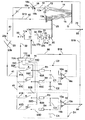
このクロック同期した信号成分の発生は2つのLED間の伝搬時間差を指示するものであり、2つのLEDへの明白な割当ても可能であるから、この情報により図1の制御回路(ないしループ、Regelkreis)(下記参照)を次のように接続することができる。すなわち、フォトダイオードに直接入射するLEDの信号を公知の手段(例えば調整可能なオールパスフィルタによる制御可能な伝搬時間、またはデジタルで調整可能な位相シフト)によって、対象物で反射される光と同じ大きさだけシフトするのである。直接的に入射するLED12に対する位相シフタ17(図1)における電気制御パルスの所要のシフトは、伝搬時間に対する直接的尺度であり、従って反射性対象物の距離に対する直接的尺度でもある。
The generation of this clock-synchronized signal component indicates the propagation time difference between the two LEDs and can also be clearly assigned to the two LEDs, so this information allows the control circuit (or loop, Regelkreis) of FIG. ) (See below) can be connected as follows. That is, the signal of the LED directly incident on the photodiode is as large as the light reflected by the object by known means (eg, controllable propagation time by an adjustable all-pass filter, or digitally adjustable phase shift). It shifts by this amount. The required shift of the electrical control pulse in the phase shifter 17 (FIG. 1) relative to the directly
伝搬時間に依存する信号成分を同期復調した後、2つの信号は直接入射するLEDの位相シフトによって相互に“0”に制御するため、例えば、もちろんさらなる高増幅率演算増幅器で相互に比較される。この演算増幅器の帯域幅には特別の要求はない。その際クロック同期される2つの信号成分にまだ小さな差が存在すれば、この差は位相制御を介して“0”に制御される。任意の増幅器を使用することができるが、有利には(交番)変化電圧増幅器(Wechselspannungsverstaerker)が使用される。 After synchronously demodulating the signal component that depends on the propagation time, the two signals are controlled to “0” by the phase shift of the directly incident LED, so that they are compared with each other by, for example, a further high-amplification operational amplifier. . There is no special requirement for the bandwidth of this operational amplifier. At this time, if there is still a small difference between the two signal components that are clock-synchronized, this difference is controlled to "0" via phase control. Any amplifier can be used, but preferably an (alternate) variable voltage amplifier (Wechselspannungsverstaerker) is used.
実施例では、図1下方の2つの異なる制御回路が同時に使用される。一方では、2つのLED区間に対する受信振幅は、2つのLEDの少なくとも1つの振幅制御によって、フォトダイオード(受信器13)の入力端で同じ値になるよう制御される。これはEP706648B1から公知のものと同様である。一方のLEDを第2のLEDに切り替えた後、振幅情報としての位相差は長さに大きく引き伸ばされるから、伝搬時間情報がすでに消失した時点で初めて信号を、クロック同期した振幅差について検査すべきである。実際には例えば100kHzから200kHzのクロック周波数が有効(適切)であることが判明している。ここで1クロック期間の第1の部分では信号が信号中の振幅として発生する伝搬時間差についてクロック制御の前に検査され、クロック期間の第2の部分では純粋に振幅差について検査される。クロック期間の第2の半分からの情報により、実施例では2つのLEDの少なくとも1つの振幅だけが調整され、2つの光区間からほぼ同じ大きさの信号が得られるようにし、これにより差値をゼロに制御する。2つの光区間の信号が同じ大きさであれば、クロック同期した(交番)変化成分(Wechselanteile)のないゼロ信号が得られる。 In the embodiment, two different control circuits at the bottom of FIG. 1 are used simultaneously. On the other hand, the reception amplitude for the two LED sections is controlled to be the same value at the input end of the photodiode (receiver 13) by controlling the amplitude of at least one of the two LEDs. This is similar to that known from EP706648B1. After switching one LED to the second LED, the phase difference as amplitude information is greatly extended in length, so the signal should be checked for clock-synchronized amplitude difference only when the propagation time information has already disappeared It is. In practice, it has been found that a clock frequency of, for example, 100 kHz to 200 kHz is effective (appropriate). Here, in the first part of one clock period, the propagation time difference generated as an amplitude in the signal is inspected before clock control, and in the second part of the clock period, the amplitude difference is inspected purely. With the information from the second half of the clock period, in the embodiment only the amplitude of at least one of the two LEDs is adjusted so that a signal of approximately the same magnitude is obtained from the two light sections, so that the difference value is obtained. Control to zero. If the signals in the two optical sections are the same, a zero signal without a clock-synchronized (alternating) change component (Wechselanteile) can be obtained.
もちろんフォトダイオードに直接入射するLEDの位相を、反射を引き起こす他方のLEDの伝搬時間に相応して適合する必要はなく、相応に回路構成すれば、反射を引き起こすLEDも調整することができる。 Of course, it is not necessary to adjust the phase of the LED directly incident on the photodiode in accordance with the propagation time of the other LED causing the reflection, and if the circuit is configured accordingly, the LED causing the reflection can be adjusted.
この2つの閉制御ループとしての
・振幅制御
・伝搬時間制御
をそれぞれの“0クロック同期”成分について行うことにより、冒頭に述べた利点が達成される。
By performing the amplitude control and propagation time control as the two closed control loops for the respective “0 clock synchronization” components, the advantages described at the beginning are achieved.
個々にアドレシング可能なピクセルを備えるカメラに適用する場合、もちろん各ピクセルに対して反射性対象物までの距離が検出される。カメラでの適用で前記のシステムは、距離、反射および画像内容に対する情報が各別に発生するという利点を提供する。距離測定はそれぞれのピクセルにおいて“0信号”を調整するから、本来の測定が外部光源(自然の日光、太陽)に基づく画像情報を妨げることはない。 When applied to a camera with individually addressable pixels, of course, the distance to the reflective object is detected for each pixel. In camera applications, the system provides the advantage that information on distance, reflection and image content is generated separately. The distance measurement adjusts the “0 signal” at each pixel, so the original measurement does not interfere with image information based on an external light source (natural sunlight, sun).
図1を参照すると、本発明の装置では光が受信器13に第2の光区間(光路)20を介して導かれ、とりわけ振幅補償部が設けられている。この方法は、とりわけカメラ10(図8)に対する光伝搬時間測定に有用である。まず光ビームがクロック制御部11により例えば200kHzに変調されて、出力端11Eから線路30,31,32を介し、さらに(光)送信器12を介して光区間14に入射される。線路30(線路31を経て)は出力制御器18の入力端に至り、その出力端18bから線路32を介して送信器12の入力端12aに至る。光は送信器12から対象物Oに達し、そこで反射されて受信器13に達する。同じクロックではあるが、インバータ22により反転されたクロックにより、補償光源としての別の送信器21または図示しない補償光源からも光は受信器13に入射される。このためにクロック制御部11の信号は線路30,33を介して位相シフタ17の入力端17aに、また位相シフタの出力端17bと線路34を介してインバータ22の入力端22aに達する。このインバータの出力端22bから信号は線路35を介して(更なる)別の送信器21の入力端21に達する。これにより受信器の出力端13aでは、クロック制御部11のクロックの変化時に2つの光区間からの信号S13が線路40に出力される。別の送信器21から発する別の信号も、図1の実施例では同様にクロック制御部11によりクロッキングされる光信号であり、この光信号は、有利には光区間14からの第1の光信号に対して平行に、受信器13に導かれる。しかしこの光信号は進行する区間(光路)長がほとんどないか、またはその距離に関して既知の区間(光路)を進行する。信号S13は線路40を介して増幅器23に供給され、増幅器で増幅され、線路41を介して同じように構成された2つの同期復調器D1、D2に導かれる。これら同期復調器は図1の下方に示されており、それぞれ比較器を備えている。ここで同期復調器D1,D2の役目は、位相を正確に検出することではなく、クロックに従って(taktweise)振幅を検出することである。位相精度は測定精度に何の影響も及ぼさない。従って例えば20°の位相ずれも無視できる。
Referring to FIG. 1, in the apparatus of the present invention, light is guided to a
これらの回路に詳細に立ち入る前に、図2の上部は増幅器23の後方に発生する信号を示していることを述べる。図示の信号は、例えば15cmの反射距離による伝搬時間がある場合の信号経過を示しており、ここでは送信器12と別の送信器21である2つのLEDの少なくとも一方の信号位相に適合していない。クロック同期した信号成分の発生は、相応のゲート回路により検出することができ、相応するLEDに対応付けることができる。その際クロック領域全体の振幅差と信号振幅とはクロックの切替直後に区別される(べきものである)。このためにクロック周期が、図2で4つの区間A/B/C/Dに分割される。区間B,Dは、クロック同期した振幅差がない場合の制御状態での振幅値を表す。すなわち振幅値はクロックからクロックへと同じである。区間B,Dの制御状態は、双方(2つ)のLEDの少なくとも一方の振幅制御に関連する。クロック区間BとDで振幅が同じ値に制御された状態では、2つのLEDの光伝搬時間が同じ場合、フォトダイオードにはクロック同期した信号成分のない信号が発生する。別の光区間20と光区間14との間に伝搬時間差がある場合だけ、クロック同期した信号成分が発生する。
Before going into details of these circuits, it will be noted that the upper part of FIG. 2 shows the signal generated behind the
図1で、比較器を備える同期復調器D1とD2はクロック制御部11により、出力端11A,11B,11C,11Dと所属のクロック線路50A,50B,50C,50Dを介して次のように制御される。すなわち(一方の)同期復調器D1は受信した信号S13におけるクロック同期した振幅差を、振幅制御のための出力制御器18を介して“0”になるように制御し、(他方の)同期復調器D2は(両)光区間の間の伝搬時間差を検出し、位相シフタ17を介してこれが“0”になるように制御する。光伝搬時間が制御されない場合には、クロック区間AとCにクロック同期した信号成分が発生し、この信号成分は位相ごとに(交番ないし極性)変化する極性を有している。この信号成分は同期復調器D2の出力端で制御信号S16となり、この制御信号S16は位相シフタ17を、増幅器23の出力端23bに、クロック同期した信号成分のない“0”信号が発生するように制御する。
In FIG. 1, synchronous demodulators D1 and D2 having comparators are controlled by a
同期復調器D1では、受信信号S13が再び2つの光区間14と20に分解される。このために信号は線路41,41B,41Dを介して、区間BとDに配属(割当て)されたスイッチに供給される。これらのスイッチはクロック線路50Bと50Dを介してクロック制御部11により、区間BとDのクロック変化時に操作される。これによりスイッチ位置に相応してスイッチの出力端では、区間BとDに相応する信号が線路60Bと60D上に発生する。これらの信号は積分器(Integrator)R3,R4および/またはC3,C4を介して比較器15の入力端15a,15bに供給される。比較器の出力端15cには、信号が同じ大きさの場合、信号S13のゼロ状態に対する相応の制御信号が発生する。そこに別の信号が発生する場合、任意の制御信号が出力制御器18による振幅制御のための信号S15として線路70を介して出力制御器18の入力端18cに生じる。この出力制御器は送信器12のビーム出力における振幅を、信号S13がゼロ状態に相応する信号になるように後(追従)制御(nachregelt)する。すなわち信号S13がクロック同期した成分を含んでおらず、それ以上の後制御が必要ないようにする。この状態でクロック同期した変化成分(Wechselanteile)は除去(ないし最小に軽減)される(eliminiert)。すなわち反射特性、外部光または温度変化により惹起される影響は光伝搬時間測定に影響を及ぼさない。図面では送信器12のビーム出力が後制御されるが、この制御はEP706648B1から公知のように(更なる)別の送信器21でも、または2つの送信器でも、または複数の送信器がある場合には複数の送信器でも行うことができることは自明である。同じことが受信器13に直接割り当てられた補償光源の場合に対しても当てはまる。従って信号S15は同時に、反射または振幅に対する信号94である。
In the synchronous demodulator D1, the received signal S13 is again decomposed into two
言い替えると、同期復調器D1はクロック区間に従って(taktabschnittweise)に振幅検出するために使用され、その入力端、すなわち区間BとDに割り当てられたスイッチには、光学的秤の2つの区間からの、有利にはすでに制御された、ゼロ信号が印加される。このために図1では、2つの光区間が相互に独立して外部に導かれる。そしてそれら光区間の振幅は、同期復調器D1の入力端で相互にすでにゼロであり、変化する信号を生じないように制御される。このことは、図1の下方に図示された、外部影響を所望の精度に必要であるよう補償するためのスイッチBとDにより行われる。次いで残ったゼロ信号から、同期復調器D2の形態にある振幅検出器の出力端でノイズ中のクロック(交番)変化信号(Taktwechselsignal)を検出することができる。 In other words, the synchronous demodulator D1 is used to detect amplitude in accordance with the clock period, and its input, ie the switch assigned to the periods B and D, is from the two sections of the optical scale, A zero signal, preferably already controlled, is applied. For this reason, in FIG. 1, the two light sections are guided to the outside independently of each other. The amplitudes of these optical sections are already zero with respect to each other at the input end of the synchronous demodulator D1, and are controlled so as not to generate a changing signal. This is done by the switches B and D shown in the lower part of FIG. 1 to compensate for external influences as required for the desired accuracy. Then, from the remaining zero signal, the clock (alternate) change signal (Taktwechselsignal) in the noise can be detected at the output end of the amplitude detector in the form of the synchronous demodulator D2.
クロック線路50A,50B,50C,50Dを介するサンプリング時点の位相変化は、広い領域にわたって距離測定には影響を及ぼさない。DE10022054A1では、同期復調器の位相に高精度が必要であるが、それに対しこのことは本発明では距離測定に関与しない。振幅のサンプリング(Abtasten)時点がほぼクロック時点(ungefaehrer Zeitpunkt des Taktes)であることが必要なだけである。従って本発明では、「同期復調」は擬似的な同期復調である。位相自体は、クロック変化信号の振幅差を識別可能にし、同期復調器D2の形態の振幅検出器の入力端における出力をゼロにするためには殆んど重要ではない。このクロック変化信号は、成分の位相シフトによって相互に最小に、有利にはゼロにされる。これにより生じる位相シフタ17の遅延は光伝搬時間である。
The phase change at the time of sampling via the clock lines 50A, 50B, 50C, 50D does not affect the distance measurement over a wide area. DE 10022054A1 requires high accuracy in the phase of the synchronous demodulator, whereas this is not involved in distance measurement in the present invention. It is only necessary that the amplitude sampling (Abtasten) time is approximately the clock time (ungefaehrer Zeitpunkt des Taktes). Therefore, in the present invention, “synchronous demodulation” is pseudo synchronous demodulation. The phase itself makes it possible to identify the amplitude difference of the clock change signal and is hardly important for zeroing the output at the input of the amplitude detector in the form of a synchronous demodulator D2. This clock change signal is minimized, preferably zero, by the phase shift of the components. The delay of the
図1中央部では、同期復調器D2の上部の2つのスイッチがゲート回路により、図2上部の領域AとCに相応して制御される。同期復調器D2では、受信信号S13が同様に2つの光区間14並びに20の振幅信号に割り当てられる。すなわち区間AとCに相応する信号区間である。このために信号は線路41,41A,41Cを介して、区間AとCに配属されたスイッチに供給される。これらのスイッチはクロック線路50Aと50Cを介してクロック制御部11により、区間AとCのクロック変化時に操作される。これによりスイッチ位置に相応してスイッチの出力端では、区間AとCに相応する信号が線路60Aと60C上に発生する。これらの信号は積分器R1,R2および/またはC1,C2を介して比較器16の入力端16a,16bに供給される。
In the central part of FIG. 1, the two switches at the top of the synchronous demodulator D2 are controlled by the gate circuit in accordance with the areas A and C at the top of FIG. In the synchronous demodulator D2, the received signal S13 is similarly assigned to the amplitude signals of the two
これによりクロックに従って(taktweise)、クロック変化の際に発生し、光区間の光伝搬時間に相応する第1の光信号と第2の信号、すなわち(さらなる)別の光信号とが検出される。これらの信号の大きさ、すなわち振幅は反射に依存するが、しかしこれら2つの信号の、クロック同期した差値の検出が問題なので、このことは何の影響もない。2つの信号は別の比較器16で比較される。この差値は、第1の光信号と第2の信号との間の位相差に相応し、フォトダイオードでの積分に基づいて振幅値に変換される。この値は、位相情報がもはや存在しない任意の時点でサンプリングすることができる。位相どおりではない、すなわち位相境界(Phasengrenze)では正確には一致しない振幅値の差値は線路80を介し信号S16として位相シフタ17の入力端17cに達し、この位相シフタ17でこれが最小に、有利にはゼロになるように変化される。そしてこれにより光伝搬時間が検出される。ここで位相シフタ17での調整された遅延から、光伝搬時間を検出することができ、ひいては距離を検出することができる。この距離は位相シフタ17の出力端17dに、伝搬時間信号93として発生する。位相シフタの変化によって、図3のようにクロック変化信号(Taktwechselsignal)TWの振幅はノイズ中に消失する。
Thereby, according to the clock (taktweise), the first optical signal and the second signal, ie (further) another optical signal, which are generated when the clock changes and correspond to the optical propagation time of the optical section, are detected. The magnitude, or amplitude, of these signals depends on the reflection, but this has no effect because the detection of the clock-synchronized difference between these two signals is a problem. The two signals are compared by another
位相シフタ17はアナログ動作する回路とすることができるが、デジタル信号遅延部とすることもできる。ここで高周波クロックは、例えばクロックが1nsステップで、ずれること(シフト)ができるように選択することができる。このために信号S16はA/D変換器によりサンプリング(ないし走査、abtasten)され、結果は相応の位相シフトに変換される。
The
図9は、別の実施例の概略的回路図を示す。この別の実施例では、第2の信号が光区間ではなく、電子的に増幅器23に供給される。この実施例で、図1の実施例と同じ構成部材および線路には同じ参照符合が使用されている。増幅器の後の構成部材、すなわち同期復調器D1とD2、およびそこで得られた結果、すなわち信号S15とS16も、92と94も同じである。同様に送信器12とその制御も、出力制御器18を除いて図1の実施例と同じであり、光区間14も同じである。しかし信号S15は線路70と71を介して分岐点に達し、この分岐点で線路72と73に導かれる。スイッチ91はクロック制御部11により、送信器12と同じ出力端11Eを介し同じクロックで、しかしインバータ22により反転して制御される。このためにクロック制御部11の信号は線路30,33を介して位相シフタの入力端17aに、また位相シフタの出力端17bと線路34を介してインバータ22の入力端22aに達する。このインバータの出力端22bから信号は線路79を介してスイッチ91に達する。これによりスイッチ下流の線路74にはクロック制御部11のクロック変化時に、線路73の信号S15または線路72を介する信号が印加される。これにより電子的に伝達された信号は光区間を進まず、従って光速度による光区間の分だけ信号S13よりも高速である。線路74上の信号は、容量C5を備える積分器R5とDC脱結合(分離)部90を介し、さらに線路75[90は誤記]と線路40を介して増幅器23に供給される。そこから信号は、図1の実施例と同じように線路41を介して、同じように構成された2つの同期復調器D1,D2に供給される。これら同期復調器は夫々比較器を備えており、信号は第1の実施例と同じように処理される。
FIG. 9 shows a schematic circuit diagram of another embodiment. In this alternative embodiment, the second signal is supplied to the
この種の非対称構成は外部の影響に鋭敏に応答する。従ってこれに対して対策を講じる必要がある。1つの手段は、受信器13として部分的に非透光に被覆されたフォトダイオードを使用することである。このために例えばフォトダイオードの縁部13bを非透光に被覆することができる。フォトダイオードに入射する光は、とりわけこれがフォトダイオードの正面に直接当たらない場合、正面に入射する光の電気信号とは異なる立上がり時間を引き起こす。このことによって測定結果に誤差が出る。
This type of asymmetric configuration is sensitive to external influences. Therefore, it is necessary to take measures against this. One means is to use a partially non-transparent photodiode as the
これまでに説明は1つのピクセルの表示に関連するものである。もちろん1つのアレイに複数ないしは多数のピクセルが配置されていても良く、これらのピクセルが光学系により観察領域を結像する。この場合、各ピクセルに対して、例えばシーケンシャルに、個々の距離が検出される。 The description so far has been related to the display of a single pixel. Of course, a plurality of or many pixels may be arranged in one array, and these pixels form an image of the observation region by the optical system. In this case, individual distances are detected for each pixel, for example, sequentially.
実際には、反射された信号と直接入射するLEDの入射角が種々異なることにより、測定結果に誤差が生じることが判明した。DE103 22 552 A1から、2つの異なる光経路(光路長)を、ほぼ同じ角度を以てフォトダイオードに衝突させるための手段が公知である。従って別の送信器21から発する光信号は半透明または透明の偏向手段25を介して偏向され、光区間14から発する光に対してほぼ平行にまたは同じ角度で受信器に入射する。有利には第2の信号は少なくとも部分的に受信器13に向けて偏向され、一方、光区間14から発する第1の光信号は実質的に変更なしで受信器に入射する。
In practice, it has been found that the measurement result has an error due to the different incident angles of the reflected signal and the directly incident LED. From DE 103 22 552 A1, means are known for causing two different light paths (light path lengths) to collide with a photodiode at approximately the same angle. Accordingly, an optical signal emitted from another
クロック制御部11は有利には50から200kHzの間のクロックにより動作する。このクロック数は、これまで従来技術で光伝搬時間測定に使用されていたクロックより格段に低い。これにより比較的に大きく有利なフォトダイオードを使用することができる。とりわけ比較的に周波数の低い増幅器により動作することができる。
The
伝搬時間測定ないしは距離測定と反射測定のために、送信されたクロック同期光信号はフォトダイオードでクロック同期したゼロ成分(Null-Anteil)に制御されるから、この測定がカメラの非クロック同期の画像情報を損なうことはない。クロック同期したゼロ成分は小さな付加的同光レベル(Gleichlichtpegel)でだけ現れる。補償制御回路での振幅制御の際に、この同光レベルは反射性対象物での反射強度と共に変化する。しかし反射の値は信号S15に含まれているから、ピクセルにより測定された本来の輝度(ないし明るさ)はこの値により相応に補正される。実際にはほとんどの場合、補正は必要ないことが判明している。これとは反対に、周囲光が欠けているときに対象物照明のために送信された光には補正が必要である。 For transmission time measurement or distance measurement and reflection measurement, the transmitted clock-synchronized optical signal is controlled by a zero-clock component (Null-Anteil) that is clock-synchronized with a photodiode, so this measurement is a non-clock-synchronized image of the camera There is no loss of information. The clock-synchronized zero component appears only at a small additional light level (Gleichlichtpegel). When the amplitude is controlled by the compensation control circuit, the same light level changes with the reflection intensity at the reflective object. However, since the reflection value is included in the signal S15, the original luminance (or brightness) measured by the pixel is corrected accordingly. In practice, it has been found that in most cases no correction is necessary. In contrast, light transmitted for object illumination when ambient light is lacking needs correction.
1つのピクセルだけを使用する場合、送信エレメントとして従来のLEDを、フォトダイオードとして大面積の低価格フォトダイオード、例えばOsram社のBPW34を使用することができる。フォトダイオード増幅器はCMOS技術で形成することができ、例えばわずか200kHzの帯域幅を有することができる。増幅器のパラメータはほとんど測定精度に関与しない。従ってここでの要求は低い。本発明では詳細に説明していないが、基準信号を従来技術によりデジタルで位相シフトする(高クロック周波数)ことを別にすれば、このシステムをわずか50から200kHzのシステムクロックにより駆動することができる。高クロック周波数をもっぱらデジタル位相シフトの発生のためにだけ使用する場合、もちろんいずれの形式の位相シフトも、例えばアナログ積分形態(in analog integrierter Form)で、用いることができる。 If only one pixel is used, a conventional LED can be used as the transmitting element, and a large-area low-cost photodiode, such as BPW34 from Osram, can be used as the photodiode. The photodiode amplifier can be formed in CMOS technology and can have a bandwidth of only 200 kHz, for example. Amplifier parameters have little to do with measurement accuracy. Therefore, the demand here is low. Although not described in detail in the present invention, the system can be driven by a system clock of only 50 to 200 kHz, except that the reference signal is digitally phase shifted (high clock frequency) according to the prior art. If a high clock frequency is used exclusively for the generation of a digital phase shift, then of course any form of phase shift can be used, for example in an analog integral form.
有利には本発明で、クロックサイクルにより任意の値を取ることのできるクロック周波数を任意の値に選択することもできる。同期不可のシステムを並列に使用する場合に生じ得る干渉を抑圧するために、任意の「周波数ホッピング」(FDMA)を問題なしに使用することができる。従ってこのシステムは簡単な手段により、ただ1つの個別の光伝搬時間測定区間を実現するのに適するだけでなく、従来のカメラ、有利にはCMOSカメラから3D能力を有するシステムを形成するのにも適する。ここで前記の本発明では、送信源の照明領域にある対象物の距離測定ではあるが、従来の画像情報も同時に使用される。 Advantageously, in the present invention, it is also possible to select a clock frequency that can take any value according to the clock cycle. Any “frequency hopping” (FDMA) can be used without problems to suppress the interference that can occur when using non-synchronized systems in parallel. The system is therefore not only suitable for realizing only one individual light propagation time measurement section by simple means, but also for forming a system with 3D capability from a conventional camera, preferably a CMOS camera. Suitable. Here, in the present invention, the conventional image information is also used at the same time, although it is a distance measurement of the object in the illumination area of the transmission source.
本発明によれば、簡単な手段と小さな送信出力を使用して、外部光および温度に対して完全に不感な光伝搬時間測定が可能であり、この光伝搬時間測定は受信信号に大きなノイズがあっても極く近傍の近接領域から最大距離まで電子回路を適合することなしに行うことができる。測定すべき対象物の反射特性も測定結果に影響を及ぼさない。ここでは基本的に送信器または補償器(すなわち例えば別の送信器または電子的補償)、または両者の位相もしくは出力が制御される。 According to the present invention, it is possible to measure an optical propagation time completely insensitive to external light and temperature by using a simple means and a small transmission power, and this optical propagation time measurement has a large noise on a received signal. Even if it exists, it can carry out without adapting an electronic circuit from the proximity | contact area | region of the near neighborhood to the maximum distance. The reflection characteristics of the object to be measured do not affect the measurement results. Here basically the phase or output of the transmitter or compensator (ie another transmitter or electronic compensation, for example) or both is controlled.
所属の装置のエレメントは、特に図1と9を参照したこれまでの説明からすでに明らかである。少なくとも送信器12は、クロック制御部11によりクロッキングされる第1の光信号を少なくとも1つの光区間14へ反射性対象物Oを介して少なくとも1つの受信器13に送信する。この受信器は、前記対象物Oの接近、存在および/または距離により変化した第1の光信号を検出する。受信器13は光区間14から到来する第1の光信号を受信する。受信器13には、第1の光信号による受信信号を検出するための手段が設けられている。さらに、クロック制御部11によりクロッキングされた第2の信号を伝送するための手段が設けられており、この第2の信号は光区間14なしで、またはその距離に関して既知の区間を介して生じる。この伝送は第1の実施例では、(更なる)別の送信器21によって別の光区間20を介して行われる。しかし図9の如く電子的に行うこともできる。比較器15はクロックに従って光区間14からの受信信号と第2の信号を比較し、比較器15の出力端に比較値を形成する。少なくとも1つの制御器18は送信信号および/または第2の信号の振幅を制御するために前記比較値を使用し、受信信号と第2の信号が少なくとも比較器の入力端で実質的に同じ大きさになるようにする。クロック変化の際に発生し、光伝搬時間に相応する、光区間14からの受信信号と第2の信号との間のクロック変化信号TWをクロックに従って検出するための手段が、ゲート回路の形態で設けられている。この光区間14からの受信信号と第2の信号は比較器15の入力端において実質的に同じ大きさに制御される。別の比較器16は、光区間14からの受信信号と第2の信号との間のクロック変化信号TWを、振幅に従って比較することによって差値S16を検出する。位相シフタ17は、差値S16が最小に、有利にはゼロになるまで、受信信号と第2の信号の位相の位相遅延を変化する。差値が最小であるときに発生した位相シフタの遅延は光伝搬時間に相応する。
The elements of the device to which it belongs are already apparent from the previous description, in particular with reference to FIGS. At least the
比較器15は、振幅検知のための同期復調器D1の一部である。クロック変化信号TWをクロックに従って検出するための手段はゲート回路であり、このゲート回路は符合の変化するクロック変化信号TWを検出し、クロック変化信号TW間の差値S16が制御回路の制御量として使用される。このゲート回路と、割当てられた比較器を備える同期復調器D1,D2の別のゲート回路は、光区間14と、第2の信号が導かれる区間からの受信信号S13を異なる領域A,B,C,Dに区分け(分割)するための手段として用いられる。
The
偏向手段25が設けられており、この偏向手段は第1の光信号と第2の信号(この信号は図1では第2の光区間から生じる同様の光信号である)を受信器13に導き、偏向された光信号が実質的に平行に、または同じ角度で受信器13に当たるように偏向する。
A deflecting means 25 is provided, which guides the first optical signal and the second signal (this signal is a similar optical signal originating from the second optical section in FIG. 1) to the
少なくとも1つの送信器12、(更なる)別の送信器21および/または補償光源として少なくとも部分的に、有利には一貫して、LEDが使用される。
LEDs are used at least in part, advantageously consistently, as at least one
前記の説明に、従属請求項と等価の領域内で変化する種々の変形、変更、適合を施すことができることは自明である。 Obviously, various modifications, changes and adaptations may be made to the above description, which vary within the scope equivalent to the dependent claims.
10 カメラ
11 クロック制御部
11A,11E,11B,11C,11D 出力端
12 送信器
12a 入力端
13 受信器
13a 出力端
14 光区間(光路)
15 比較器
15a,15b 入力端
15c 出力端
S15 比較器15後方(下流)の信号
16 (更なる)別の比較器
16a,16b 入力端
16c 出力端
S16 比較器16後方の差値
17 位相シフタ
17a,17c 入力端
17b、17d 出力端
18 出力制御器
18a,18c 入力端
18b 出力端
20 (更なる)別の光区間
21 (更なる)別の送信器
21a 入力端
22 インバータ
22a 入力端
22b 出力端
23 増幅器
23a 入力端
23b 出力端
24 ピクセル
25 偏向手段
D1,D2 同期復調器
O 対象物
R1〜R5 積分器
TW クロック変化信号
30〜35 線路
40,41 線路
41A,41B,41C,41D 線路
50A,50B,50C,50D クロック線路
60A,60B,60C,50D クロック線路
75〜75,79,80 線路
90 DC分離部(脱結合部)
91 スイッチ
93 信号伝搬時間
94 信号反射
DESCRIPTION OF
15
91
Claims (27)
・クロック制御部(11)によりクロッキングされる第1の光信号を少なくとも1つの送信器(12)から少なくとも1つの光区間(14)へ、反射性対象物(O)を介して少なくとも1つの受信器(13)に送信するステップ、
ただし前記受信器は、前記対象物(O)の接近、滞留(停止)および/または離隔(Entfernung)により変化した前記第1の光信号を検出するものである、
・前記光区間(14)から到来する前記第1の光信号を、少なくとも1つの受信器(13)により受信するステップ、
・前記第1の光信号の結果である受信信号を受信器(13)で検出するステップ、
・クロック制御部(11)によりクロッキングされた第2の信号を伝送するステップ、
ただし前記第2の信号は前記光区間(14)なしで、またはその距離(離隔)に関して既知の区間を介して生じる、
・前記光区間(14)からの受信信号と前記第2の信号をクロックに従って比較し、比較値を比較器(15)の出力端に形成するステップ、
ただし前記比較器は、前記送信信号および/または前記第2の信号の振幅値を制御するために使用され、これにより前記受信信号と前記第2の信号とが少なくとも前記比較器の入力端で実質的に同じ大きさになるようにする、
・クロック変化の際に発生し、光伝搬時間に相応する、前記光区間(14)からの前記受信信号と前記第2の信号との間のクロック変化信号(TW)をクロックに従って検出するステップ、
ここで前記光区間(14)からの前記受信信号と前記第2の信号は前記比較器(15)の入力端において実質的に同じ大きさに制御される、
・前記光区間(14)からの前記受信信号と前記第2の信号との間のクロック変化信号(TW)をその振幅に従い、別の比較器(16)で比較することによって差値(S16)を検出するステップ、
・位相シフタ(17)によって、前記差値(S16)が最小に、有利にはゼロになるまで、前記受信信号と前記第2の信号の位相の位相遅延を変化するステップ、
・前記差値が最小であるときに発生した位相シフタの遅延を光伝搬時間の検出に使用するステップ、
を有することを特徴とする方法。 In particular, a method for measuring light propagation time for a camera (10) comprising the following steps:
At least one first optical signal clocked by the clock controller (11) from at least one transmitter (12) to at least one optical section (14) via a reflective object (O) Transmitting to the receiver (13);
However, the receiver detects the first optical signal changed due to approach, stay (stop) and / or separation (Entfernung) of the object (O).
Receiving the first optical signal coming from the optical section (14) by at least one receiver (13);
Detecting at the receiver (13) a received signal that is the result of the first optical signal;
Transmitting the second signal clocked by the clock controller (11);
However, the second signal is generated without the light section (14) or through a section known with respect to its distance (separation).
Comparing the received signal from the optical section (14) with the second signal according to a clock and forming a comparison value at the output of the comparator (15);
However, the comparator is used to control the amplitude value of the transmission signal and / or the second signal, whereby the reception signal and the second signal are substantially transmitted at least at the input end of the comparator. To be the same size,
Detecting a clock change signal (TW) between the received signal from the optical section (14) and the second signal, which occurs at the time of a clock change, corresponding to the optical propagation time, according to the clock;
Here, the received signal and the second signal from the optical section (14) are controlled to have substantially the same magnitude at the input end of the comparator (15).
A difference value (S16) is obtained by comparing the clock change signal (TW) between the received signal and the second signal from the optical section (14) with another comparator (16) according to the amplitude. Detecting step,
Changing the phase delay of the phase of the received signal and the second signal by the phase shifter (17) until the difference value (S16) is minimized, preferably zero,
Using the phase shifter delay generated when the difference value is minimum to detect the optical propagation time;
A method characterized by comprising:
前記第2の信号は、第2の光区間から少なくとも1つの受信器(13)によって受信された受信信号である、ことを特徴とする方法。 The method of claim 1, wherein
Method according to claim 1, characterized in that the second signal is a received signal received by at least one receiver (13) from a second optical interval.
前記第2の信号を、電子的区間(線路)を介して伝送する、ことを特徴とする方法。 The method of claim 1, wherein
A method of transmitting the second signal through an electronic section (line).
前記光区間(14)からの前記受信信号と前記第2の信号との比較は、振幅検出のための同期復調器(D1)の比較器(15)の出力端に比較値を形成するために行い、
前記比較値は、送信信号および/または第2の信号の振幅値を制御するために使用され、これにより前記光区間(14)からの受信信号と前記第2の信号とは実質的に同じ大きさになり、
同時に、反射率、外部光および温度の影響が、前記信号(S15)を前記比較器(15)の出力端で、少なくとも1つの送信器(12)の光出力を調整することによりゼロ状態に制御することによって補償される、ことを特徴とする方法。 The method according to any one of claims 1 to 3, wherein
The comparison between the received signal from the optical section (14) and the second signal is to form a comparison value at the output terminal of the comparator (15) of the synchronous demodulator (D1) for amplitude detection. Done
The comparison value is used to control the amplitude value of the transmitted signal and / or the second signal, so that the received signal from the optical section (14) and the second signal are substantially the same magnitude. Soon,
At the same time, the influence of reflectivity, external light and temperature is controlled to zero by adjusting the light output of at least one transmitter (12) with the signal (S15) at the output of the comparator (15). A method characterized by being compensated by.
前記光区間(14)からの受信信号と前記第2の信号とが少なくとも前記比較器(15)の入力端で実質的に同じ大きさである場合、増幅器(23)の出力端には、クロック同期した変化成分のない送信器からのノイズだけが存在する、ことを特徴とする方法。 The method according to any one of claims 1 to 4, wherein
When the received signal from the optical section (14) and the second signal are substantially the same size at least at the input end of the comparator (15), the output end of the amplifier (23) A method characterized in that there is only noise from a transmitter without synchronized change components.
クロック変化の際に発生し、前記光区間(14)での光伝搬時間に相応する、第1の光信号と第2の信号との間、ないしは第2の信号と光信号との間のクロック変化信号(TW)をクロックに従って検出する際、制御された状態のノイズ中のクロック変化信号の振幅は、前記比較器(15)の入力端において受信信号と第2の信号とが実質的に同じ大きさになるよう制御される、ことを特徴とする方法。 The method according to any one of claims 1 to 5, wherein
A clock generated between the first optical signal and the second signal, or between the second signal and the optical signal, which is generated when the clock changes and corresponds to the optical propagation time in the optical section (14). When detecting the change signal (TW) according to the clock, the amplitude of the clock change signal in the controlled noise is substantially the same as the received signal and the second signal at the input of the comparator (15). A method characterized by being controlled to a size.
受信器(13)として、部分的に、有利にはその縁部(13b)において、非透光性に被覆されたフォトダイオードが使用される、ことを特徴とする方法。 The method according to claim 1, wherein
Method characterized in that a non-translucently coated photodiode is used as the receiver (13), in part, preferably at its edge (13b).
前記クロック変化信号(TW)の振幅が検出され、
制御ループは前記位相シフタ(17)を、前記クロック変化信号が最小になるように制御する、ことを特徴とする方法。 The method according to any one of claims 1 to 7, wherein
The amplitude of the clock change signal (TW) is detected;
A control loop controls the phase shifter (17) to minimize the clock change signal.
符合が変化するクロック変化信号(TW)はゲート回路によって検出され、
前記クロック変化信号(TW)の間の差値(S16)は、制御ループの制御量として使用され、これにより前記差値(S16)はゼロに制御され、これにより前記位相シフタの(調整)位置が検出される、ことを特徴とする方法。 The method according to any one of claims 1 to 8,
A clock change signal (TW) whose sign changes is detected by a gate circuit,
The difference value (S16) between the clock change signals (TW) is used as a control amount of the control loop, whereby the difference value (S16) is controlled to zero, thereby the (adjustment) position of the phase shifter. Is detected.
前記光伝搬時間を測定するために、前記送信器(12,21)の切替後の振幅が測定され、前記位相シフタ(17)によってゼロに制御される、ことを特徴とする方法。 10. A method according to any one of claims 1 to 9,
Method for measuring the light propagation time, wherein the amplitude after switching of the transmitter (12, 21) is measured and controlled to zero by the phase shifter (17).
前記振幅をゼロに制御したときに発生する位相シフトは、前記対象物の距離に相当する、ことを特徴とする方法。 The method of claim 10, wherein
The phase shift that occurs when the amplitude is controlled to zero corresponds to the distance of the object.
前記光区間(14)からの受信信号(S13)と、前記第2の信号が導かれる区間からの受信信号とは種々異なる領域(A,B,C,D)に分割され、
クロック変化の領域(A,C)の間にある領域(B,D)は、ゲート回路によって前記クロック制御部(11)のクロックで、前記光区間(14)からの受信信号と第2の信号とを比較し、比較値を前記比較器(15)の出力端に形成するために使用され、
前記比較値は、前記光区間(14)からの受信信号および/または第2の信号の振幅値を制御するために使用され、当該制御より前記光区間(14)の受信信号と前記第2の信号とは実質的に同じ大きさになり、前記差値はゼロになる、ことを特徴とする方法。 12. The method according to any one of claims 1 to 11, wherein
The received signal (S13) from the optical section (14) and the received signal from the section from which the second signal is guided are divided into different regions (A, B, C, D),
The regions (B, D) between the clock change regions (A, C) are the clocks of the clock controller (11) by the gate circuit, and the received signal and the second signal from the optical section (14). And is used to form a comparison value at the output of the comparator (15),
The comparison value is used to control the amplitude value of the received signal and / or the second signal from the optical section (14), and the received signal of the optical section (14) and the second signal are controlled by the control. The method is characterized in that the signal is substantially the same size and the difference value is zero.
前記第1の光信号と、光信号として同様に第2の光区間から生じる第2の信号とは偏向手段(25)を介して受信器13に導かれ、
前記偏向手段は、偏向された光信号が実質的に平行に、または同じ角度で受信器13に当たるように偏向する、ことを特徴とする方法。 13. A method according to any one of claims 1, 2 or 4 to 12,
The first optical signal and the second signal generated from the second optical section in the same manner as an optical signal are guided to the receiver 13 via the deflecting means (25),
The method characterized in that the deflecting means deflects the deflected optical signals to impinge on the receiver 13 substantially in parallel or at the same angle.
前記対象物の種々異なる反射特性を調整するために、前記少なくとも1つの送信器(12)および別の送信器(21)および/または補償光源が前記受信器(13)において同じ振幅になるよう制御される、ことを特徴とする方法。 14. A method according to any one of claims 1 to 13, wherein
Control the at least one transmitter (12) and another transmitter (21) and / or compensating light source to have the same amplitude in the receiver (13) to adjust different reflection characteristics of the object. A method characterized by that.
振幅を制御するためにLEDの少なくとも1つが制御され、前記LEDは前記少なくとも1つの送信器(12)、前記別の送信器(21)および/または補償光源として設けられている、ことを特徴とする方法。 The method of claim 14, wherein
At least one of the LEDs is controlled to control the amplitude, said LED being provided as said at least one transmitter (12), said another transmitter (21) and / or a compensating light source how to.
発生する制御電圧は、前記対象物の反射を検出するための測定値として使用される、ことを特徴とする方法。 The method according to claim 14 or 15, wherein
The generated control voltage is used as a measurement value for detecting reflection of the object.
前記クロック変化の領域(A,C)で検出された信号は距離測定のために使用される、ことを特徴とする方法。 The method according to any one of claims 1 to 16, wherein
Method according to claim 1, characterized in that the signals detected in the clock change areas (A, C) are used for distance measurement.
・クロック制御部(11)を備え、
・前記クロック制御部(11)によりクロッキングされる第1の光信号を少なくとも1つの光区間(14)へ、反射する対象物(O)を介して少なくとも1つの受信器(13)に送信する少なくとも1つの送信器(12)を備え、
前記受信器(13)は、前記対象物(O)の接近、滞留(停止)および/または離隔(Entfernung)により変化した第1の光信号を検出するものであり、
・前記光区間(14)から到来する前記第1の光信号を受信するための少なくとも1つの受信器(13)を備え、
・前記第1の光信号の結果である受信信号を検出する手段を前記受信器(13)に備え、
・前記クロック制御部(11)によりクロッキングされた第2の信号を伝送する手段を備え、
前記第2の信号は前記光区間(14)なしで、またはその距離に関して既知の区間を介して生じるものであり、
・クロックに従って前記光区間(14)からの受信信号と前記第2の信号とを比較し、その出力端に比較値を形成する比較器(15)を備え、
・前記送信信号および/または前記第2の信号の振幅を制御するために前記比較値を使用し、前記受信信号と前記第2の信号が少なくとも前記比較器の入力端で実質的に同じ大きさになるようにする少なくとも1つの制御器(18)を備え、
・クロック変化の際に発生し、光伝搬時間に相応する、前記光区間(14)からの前記受信信号と前記第2の信号との間のクロック変化信号(TW)をクロックに従って検出する手段を備え、
ここで前記光区間(14)からの前記受信信号と前記第2の信号は前記比較器(15)の入力端において実質的に同じ大きさに制御され、
・前記光区間(14)からの前記受信信号と前記第2の信号との間のクロック変化信号(TW)を、その振幅に従い比較することによって差値(S16)を検出する別の比較器を備え、
・前記差値(S16)が最小に、有利にはゼロになるまで、前記受信信号と前記第2の信号の位相の位相遅延を変化する位相シフタ(17)を備え、
・前記差値が最小であるときに発生した前記位相シフタの遅延を光伝搬時間の検出に使用する手段を備える、
ことを特徴とする装置。 In particular, a light propagation time measuring device for a camera (10),
-It has a clock control unit (11),
Transmitting the first optical signal clocked by the clock control unit (11) to at least one optical section (14) via the reflecting object (O) to at least one receiver (13); Comprising at least one transmitter (12);
The receiver (13) detects a first optical signal changed by approaching, staying (stopping) and / or separating (Entfernung) the object (O),
Comprising at least one receiver (13) for receiving the first optical signal coming from the optical section (14);
The receiver (13) comprises means for detecting a received signal that is a result of the first optical signal;
A means for transmitting the second signal clocked by the clock controller (11);
The second signal is generated without the light section (14) or through a section known with respect to its distance;
A comparator (15) for comparing the received signal from the optical section (14) with the second signal according to a clock and forming a comparison value at an output end thereof;
Using the comparison value to control the amplitude of the transmitted signal and / or the second signal, wherein the received signal and the second signal are at least substantially the same magnitude at the input of the comparator; Comprising at least one controller (18) to be
Means for detecting a clock change signal (TW) between the received signal from the optical section (14) and the second signal, which is generated when the clock changes and corresponds to the optical propagation time, according to the clock; Prepared,
Here, the received signal and the second signal from the optical section (14) are controlled to have substantially the same magnitude at the input end of the comparator (15),
Another comparator for detecting the difference value (S16) by comparing the clock change signal (TW) between the received signal from the optical section (14) and the second signal according to the amplitude thereof. Prepared,
A phase shifter (17) for changing the phase delay of the phase of the received signal and the second signal until the difference value (S16) is minimized, preferably zero,
-Means for using the delay of the phase shifter generated when the difference value is minimum to detect the optical propagation time;
A device characterized by that.
前記第2の信号を第2の光区間へ、少なくとも1つの受信器(13)に送信する別の送信器(21)が設けられている、ことを特徴とする装置。 The apparatus of claim 18.
Device, characterized in that another transmitter (21) is provided for transmitting the second signal to the second optical section to at least one receiver (13).
前記第2の信号を、電子的区間を介して伝送する手段が設けられている、ことを特徴とする装置。 The apparatus of claim 18.
Means for transmitting the second signal via an electronic section are provided.
前記比較器(15)は、振幅検知のための同期復調器(D1)の一部である、ことを特徴とする装置。 21. The device according to any one of claims 18-20.
The device (15) characterized in that the comparator (15) is part of a synchronous demodulator (D1) for amplitude detection.
前記光区間(14)からの受信信号と前記第2の信号とが少なくとも前記比較器(15)の入力端で実質的に同じ大きさである場合、増幅器(23)の出力端には、クロック同期した変化成分のない送信器からのノイズだけが存在する、ことを特徴とする装置。 The device according to any one of claims 18 to 21,
When the received signal from the optical section (14) and the second signal are substantially the same size at least at the input end of the comparator (15), the output end of the amplifier (23) An apparatus characterized in that there is only noise from a transmitter without synchronized change components.
前記受信器(13)は、部分的に有利にはその縁部(13b)において非透光性に被覆されたフォトダイオードである、ことを特徴とする装置。 23. The device according to any one of claims 18 to 22,
Device according to claim 1, characterized in that the receiver (13) is partly advantageously a non-transparent photodiode at its edge (13b).
クロック変化信号(TW)をクロック毎に検出するための手段はゲート回路であり、
該ゲート回路は符合の変化するクロック変化信号(TW)を検出し、
クロック変化信号(TW)間の差値(S16)は制御ループの制御量として使用される、ことを特徴とする装置。 24. A device as claimed in any one of claims 18 to 23.
The means for detecting the clock change signal (TW) for each clock is a gate circuit,
The gate circuit detects a clock change signal (TW) whose sign changes,
The difference value (S16) between the clock change signals (TW) is used as a control amount of the control loop.
前記光区間(14)からの受信信号(S13)と、前記第2の信号が導かれる区間からの受信信号とを種々異なる領域(A,B,C,D)に分割する手段が設けられており、
クロック変化の領域(A,C)の間にある領域(B,D)をクロックに従って検出するための手段としてゲート回路が設けられている、ことを特徴とする装置。 25. Apparatus according to any one of claims 18 to 24,
Means are provided for dividing the received signal (S13) from the optical section (14) and the received signal from the section from which the second signal is guided into different regions (A, B, C, D). And
A device comprising a gate circuit as means for detecting an area (B, D) between clock change areas (A, C) according to a clock.
偏向手段(25)が設けられており、
該偏向手段は前記第1の光信号と、光信号として同様に第2の光区間から生じる前記第2の信号を前記受信器(13)に導き、偏向された光信号が実質的に平行に、または同じ角度で前記受信器(13)に当たるように偏向する、ことを特徴とする装置。 26. The device according to any one of claims 18, 19 or 21 to 25,
Deflection means (25) are provided,
The deflecting means guides the first optical signal and the second signal similarly generated as the optical signal from the second optical section to the receiver (13), so that the deflected optical signal is substantially parallel. Or deflecting to strike the receiver (13) at the same angle.
前記少なくとも1つの送信器(12)、前記別の送信器(21)および/または前記補償光源は少なくとも部分的に、LEDによって構成されている、ことを特徴とする装置。 27. The device according to any one of claims 18 to 26,
The device characterized in that the at least one transmitter (12), the further transmitter (21) and / or the compensating light source are at least partly constituted by LEDs.
Applications Claiming Priority (3)
| Application Number | Priority Date | Filing Date | Title |
|---|---|---|---|
| DE102005036354 | 2005-07-29 | ||
| DE102005045993A DE102005045993B4 (en) | 2005-07-29 | 2005-09-27 | Method for measuring the time of flight |
| PCT/EP2006/007549 WO2007012501A1 (en) | 2005-07-29 | 2006-07-29 | Method for light propagation time measurement |
Publications (2)
| Publication Number | Publication Date |
|---|---|
| JP2009503470A true JP2009503470A (en) | 2009-01-29 |
| JP2009503470A5 JP2009503470A5 (en) | 2010-01-28 |
Family
ID=36972857
Family Applications (1)
| Application Number | Title | Priority Date | Filing Date |
|---|---|---|---|
| JP2008523264A Pending JP2009503470A (en) | 2005-07-29 | 2006-07-29 | Measuring method of light propagation time |
Country Status (10)
| Country | Link |
|---|---|
| US (1) | US7821618B2 (en) |
| EP (1) | EP1913420B1 (en) |
| JP (1) | JP2009503470A (en) |
| AT (1) | ATE511108T1 (en) |
| DE (1) | DE102005045993B4 (en) |
| DK (1) | DK1913420T3 (en) |
| PL (1) | PL1913420T3 (en) |
| PT (1) | PT1913420E (en) |
| SI (1) | SI1913420T1 (en) |
| WO (1) | WO2007012501A1 (en) |
Cited By (8)
| Publication number | Priority date | Publication date | Assignee | Title |
|---|---|---|---|---|
| JP2011511261A (en) * | 2007-01-29 | 2011-04-07 | ライメ、ゲルト | Method and apparatus for determining the distance to a reflective object |
| WO2012073378A1 (en) * | 2010-12-03 | 2012-06-07 | ジックオプテックス株式会社 | Optical distance measurement device |
| WO2013014761A1 (en) | 2011-07-27 | 2013-01-31 | ジックオプテックス株式会社 | Optical wave distance measurement device |
| KR101460917B1 (en) | 2010-07-06 | 2014-11-13 | 메카레스 시스템스 게엠베하 | Optoelectronic measuring arrangement having a compensation light source |
| JP2015505034A (en) * | 2011-12-06 | 2015-02-16 | エルモス セミコンダクタ アーゲー | Method for measuring a transmission line by compensating amplitude measurements and delta-sigma method and device for carrying out said method |
| JP2015514968A (en) * | 2012-02-23 | 2015-05-21 | エルモス セミコンダクタ アーゲー | Method and sensor system for measuring the characteristics of a transmission line of a measuring device between a transmitter and a receiver |
| JP2016502657A (en) * | 2012-11-08 | 2016-01-28 | ブルーテックニックス ゲーエムベーハー | Recording method using at least two Time-of-flight cameras |
| WO2018159289A1 (en) * | 2017-02-28 | 2018-09-07 | ソニーセミコンダクタソリューションズ株式会社 | Distance measurement device, distance measurement method, and distance measurement system |
Families Citing this family (39)
| Publication number | Priority date | Publication date | Assignee | Title |
|---|---|---|---|---|
| US20080111607A1 (en) * | 2006-11-10 | 2008-05-15 | Hart Robert T | Amplitude-linear differential phase shift circuit |
| DE102006057495A1 (en) * | 2006-12-06 | 2008-08-21 | Valeo Schalter Und Sensoren Gmbh | Method for detecting a physical quantity and device therefor |
| US8063790B2 (en) * | 2009-07-10 | 2011-11-22 | Rothenberger David C | System and method for detecting the presence of an object |
| JP5725979B2 (en) * | 2011-06-03 | 2015-05-27 | キヤノン株式会社 | Imaging apparatus and control method thereof |
| EP2597482A1 (en) | 2011-11-22 | 2013-05-29 | ELMOS Semiconductor AG | Device and sensor for distance measurement using the duration of compensated pulses |
| KR101851427B1 (en) | 2012-02-03 | 2018-04-23 | 메카레스 시스템스 게엠베하 | Compensation of an optical sensor via printed circuit board |
| DE102012024597B4 (en) | 2012-12-13 | 2014-07-24 | Elmos Semiconductor Ag | Time-resolved delay measurement system |
| EP2936201B1 (en) | 2012-12-21 | 2020-04-15 | Elmos Semiconductor Aktiengesellschaft | Device for determining a property of a transmission channel between a transmitter and a receiver |
| DE102012025466A1 (en) | 2012-12-28 | 2014-07-03 | Valeo Schalter Und Sensoren Gmbh | Method for distinguishing between a target object and an atmospheric component during a measurement with the aid of an optoelectronic sensor device of a motor vehicle, sensor device and motor vehicle |
| DE102012025464A1 (en) | 2012-12-28 | 2014-07-03 | Valeo Schalter Und Sensoren Gmbh | Optoelectronic sensor device for e.g. passenger car, has aperture stop and light trapping structure for preventing impingement of scattered radiation to receiver and for preventing crosstalk between optical transmitter and receiver |
| DE102012025467A1 (en) | 2012-12-28 | 2014-07-03 | Valeo Schalter Und Sensoren Gmbh | Optoelectronic sensor device, particularly visibility sensor for motor vehicle, has measuring unit measuring intensity loss of radiation based on pollution of disk, where evaluation device determines reflecting power |
| WO2014170118A1 (en) | 2013-04-17 | 2014-10-23 | Mechaless Systems Gmbh | Method for optically measuring distances in the near and far range |
| DE102013013664B3 (en) * | 2013-08-17 | 2014-08-14 | Elmos Semiconductor Ag | Time resolution delay measurement system has controller whose control characteristic is selected, such that amplitude of receiver output signal and parasitic elements of system caused control error are considered as constant |
| EP3124993B1 (en) | 2013-08-22 | 2021-10-06 | Elmos Semiconductor SE | Disturbance-compensated device for measuring an optical signal transfer route |
| DE202014010352U1 (en) | 2013-09-12 | 2015-06-17 | Mechaless Systems Gmbh | Gesture recognition device |
| DE102014106463A1 (en) * | 2014-05-08 | 2015-11-12 | Sick Ag | Distance measuring sensor and method for detection and distance determination of objects |
| DE102015002270A1 (en) | 2014-05-09 | 2015-11-26 | Elmos Semiconductor Aktiengesellschaft | Device and method for in particular three-dimensional optical scanning, measuring and classifying objects and for object recognition by means of light transit time measurement |
| DE102014019709A1 (en) | 2014-05-19 | 2015-11-19 | Elmos Semiconductor Aktiengesellschaft | Method for operating a mechanical device |
| DE102014019708A1 (en) | 2014-05-19 | 2015-11-19 | Elmos Semiconductor Aktiengesellschaft | Method for operating a mechanical device |
| DE102014017237A1 (en) | 2014-11-21 | 2016-05-25 | Mechaless Systems Gmbh | Measuring system for energy-saving optical distance measurement |
| DE102014019172B4 (en) | 2014-12-17 | 2023-12-07 | Elmos Semiconductor Se | Device and method for distinguishing between solid objects, cooking fumes and smoke using a compensating optical measuring system |
| DE102014019773B4 (en) | 2014-12-17 | 2023-12-07 | Elmos Semiconductor Se | Device and method for distinguishing between solid objects, cooking fumes and smoke using the display of a mobile telephone |
| DE102015006174B3 (en) * | 2015-05-08 | 2016-08-11 | Elmos Semiconductor Aktiengesellschaft | Device and method for measuring an optical, capacitive, inductive transmission path |
| DE102015015244A1 (en) | 2015-11-18 | 2017-05-18 | Elmos Semiconductor Aktiengesellschaft | Simple gesture recognition device |
| DE102015015248A1 (en) | 2015-11-18 | 2017-05-18 | Elmos Semiconductor Aktiengesellschaft | Simple gesture recognition device |
| DE102015015246A1 (en) | 2015-11-18 | 2017-05-18 | Elmos Semiconductor Aktiengesellschaft | Simple gesture recognition device |
| DE102015015389A1 (en) | 2015-11-18 | 2017-05-18 | Elmos Semiconductor Ag | Simple gesture recognition device |
| DE102015015245A1 (en) | 2015-11-18 | 2017-05-18 | Elmos Semiconductor Aktiengesellschaft | Simple gesture recognition device |
| DE102015015390A1 (en) | 2015-11-18 | 2017-05-18 | Elmos Semiconductor Ag | Simple gesture recognition device |
| DE102016103690B3 (en) * | 2016-03-01 | 2017-05-18 | Elmos Semiconductor Aktiengesellschaft | Optical transit time measurement according to a one- or two-stage delta-sigma method |
| DE102016103688B3 (en) * | 2016-03-01 | 2017-05-18 | Elmos Semiconductor Aktiengesellschaft | Optical transit time measurement according to a one- or two-stage delta-sigma method and associated device |
| DE102017106813B4 (en) | 2016-05-09 | 2018-01-18 | Elmos Semiconductor Aktiengesellschaft | Device and associated method for autonomous address configuration of configurable, flexible sensor bands |
| DE102017106812B4 (en) | 2016-05-09 | 2018-01-11 | Elmos Semiconductor Aktiengesellschaft | Device and associated method for autonomous address configuration of configurable, flexible LED sensor strips |
| DE102017106811B4 (en) | 2016-05-09 | 2018-01-11 | Elmos Semiconductor Aktiengesellschaft | Device and associated method for autonomous address configuration of configurable, flexible LED strips |
| DE102017100308B3 (en) | 2016-12-06 | 2018-05-30 | Elmos Semiconductor Aktiengesellschaft | Device and method for measuring an optical, capacitive, inductive transmission path with reduced EMC sensitivity |
| DE102017100305B4 (en) | 2017-01-09 | 2021-08-12 | Elmos Semiconductor Se | Device and method for measuring an optical, capacitive, inductive transmission path by means of multiple modulation |
| DE102017100306B4 (en) | 2017-01-09 | 2021-08-12 | Elmos Semiconductor Se | Device and method for measuring an optical, capacitive, inductive transmission path by means of multiple modulation |
| EP3525004B1 (en) * | 2018-02-08 | 2020-10-14 | Cedes AG | Tof sensor with test transmitter |
| CN108508451A (en) * | 2018-04-03 | 2018-09-07 | 深圳新亮智能技术有限公司 | The pulsed laser ranging sensor of High-precision high-frequency time |
Family Cites Families (10)
| Publication number | Priority date | Publication date | Assignee | Title |
|---|---|---|---|---|
| JP2896782B2 (en) * | 1988-12-30 | 1999-05-31 | 株式会社トプコン | Pulse type lightwave distance meter |
| JP3362852B2 (en) * | 1993-07-02 | 2003-01-07 | ライメ、ゲルト | Device for measuring or identifying changes in reflective elements |
| US5796098A (en) * | 1995-09-29 | 1998-08-18 | Board Of Supervisors Of Louisiana State University And Agricultural And Mechanical College | Sensor for rotational velocity and rotational acceleration |
| DE19616038A1 (en) * | 1996-04-23 | 1997-10-30 | Bosch Gmbh Robert | Method and measuring device for determining the position of an object |
| DE10001955A1 (en) | 2000-01-18 | 2001-07-19 | Gerd Reime | Optoelectronic switch evaluates variation in received light signal for operating switch element when movement of switch operating object conforms to given movement pattern |
| DE10022054B4 (en) * | 2000-05-06 | 2006-05-24 | Leuze Electronic Gmbh & Co Kg | Optical distance sensor |
| DE10025844A1 (en) * | 2000-05-25 | 2001-12-06 | Adc Automotive Dist Control | Method for determining the distance between a reference object and at least one target object |
| DE10133823A1 (en) | 2001-07-16 | 2003-02-27 | Gerd Reime | Optoelectronic device for position and movement detection and associated method |
| DE10300223B3 (en) | 2003-01-03 | 2004-06-24 | Gerd Reime | Optoelectronic measuring device with stray light compensation provided by intensity regulation of additional light source |
| DE10322552A1 (en) * | 2003-05-20 | 2004-12-30 | Gerd Reime | Method and device for measuring a modulated light signal |
-
2005
- 2005-09-27 DE DE102005045993A patent/DE102005045993B4/en active Active
-
2006
- 2006-07-29 SI SI200631081T patent/SI1913420T1/en unknown
- 2006-07-29 JP JP2008523264A patent/JP2009503470A/en active Pending
- 2006-07-29 EP EP06776514A patent/EP1913420B1/en active Active
- 2006-07-29 PT PT06776514T patent/PT1913420E/en unknown
- 2006-07-29 WO PCT/EP2006/007549 patent/WO2007012501A1/en active Application Filing
- 2006-07-29 US US11/997,273 patent/US7821618B2/en active Active
- 2006-07-29 DK DK06776514.9T patent/DK1913420T3/en active
- 2006-07-29 PL PL06776514T patent/PL1913420T3/en unknown
- 2006-07-29 AT AT06776514T patent/ATE511108T1/en active
Cited By (13)
| Publication number | Priority date | Publication date | Assignee | Title |
|---|---|---|---|---|
| JP2011511261A (en) * | 2007-01-29 | 2011-04-07 | ライメ、ゲルト | Method and apparatus for determining the distance to a reflective object |
| KR101460917B1 (en) | 2010-07-06 | 2014-11-13 | 메카레스 시스템스 게엠베하 | Optoelectronic measuring arrangement having a compensation light source |
| WO2012073378A1 (en) * | 2010-12-03 | 2012-06-07 | ジックオプテックス株式会社 | Optical distance measurement device |
| WO2013014761A1 (en) | 2011-07-27 | 2013-01-31 | ジックオプテックス株式会社 | Optical wave distance measurement device |
| JP2017223707A (en) * | 2011-12-06 | 2017-12-21 | エルモス セミコンダクタ アーゲー | Method for measuring transmission path by compensating amplitude measurement, and delta-sigma method and device for implementing the method |
| JP2015505034A (en) * | 2011-12-06 | 2015-02-16 | エルモス セミコンダクタ アーゲー | Method for measuring a transmission line by compensating amplitude measurements and delta-sigma method and device for carrying out said method |
| JP2015514968A (en) * | 2012-02-23 | 2015-05-21 | エルモス セミコンダクタ アーゲー | Method and sensor system for measuring the characteristics of a transmission line of a measuring device between a transmitter and a receiver |
| JP2016502657A (en) * | 2012-11-08 | 2016-01-28 | ブルーテックニックス ゲーエムベーハー | Recording method using at least two Time-of-flight cameras |
| WO2018159289A1 (en) * | 2017-02-28 | 2018-09-07 | ソニーセミコンダクタソリューションズ株式会社 | Distance measurement device, distance measurement method, and distance measurement system |
| CN110168403A (en) * | 2017-02-28 | 2019-08-23 | 索尼半导体解决方案公司 | Distance-measuring device, distance measurement method and Range Measurement System |
| JPWO2018159289A1 (en) * | 2017-02-28 | 2019-12-19 | ソニーセミコンダクタソリューションズ株式会社 | Distance measuring device, distance measuring method, and distance measuring system |
| JP7027403B2 (en) | 2017-02-28 | 2022-03-01 | ソニーセミコンダクタソリューションズ株式会社 | Distance measuring device and distance measuring method |
| CN110168403B (en) * | 2017-02-28 | 2023-12-01 | 索尼半导体解决方案公司 | Distance measuring device, distance measuring method, and distance measuring system |
Also Published As
| Publication number | Publication date |
|---|---|
| WO2007012501A1 (en) | 2007-02-01 |
| DE102005045993A1 (en) | 2007-02-01 |
| PL1913420T3 (en) | 2011-10-31 |
| SI1913420T1 (en) | 2011-09-30 |
| US7821618B2 (en) | 2010-10-26 |
| US20080204700A1 (en) | 2008-08-28 |
| PT1913420E (en) | 2011-09-01 |
| ATE511108T1 (en) | 2011-06-15 |
| DK1913420T3 (en) | 2011-09-05 |
| EP1913420B1 (en) | 2011-05-25 |
| DE102005045993B4 (en) | 2008-11-13 |
| EP1913420A1 (en) | 2008-04-23 |
Similar Documents
| Publication | Publication Date | Title |
|---|---|---|
| JP2009503470A (en) | Measuring method of light propagation time | |
| US8405821B2 (en) | Method and device for determining the distance to a retroreflective object | |
| WO2020042166A1 (en) | Time of flight-based distance measurement method and distance measurement system | |
| US9599713B2 (en) | Distance-measuring device | |
| EP3072162B1 (en) | Lidar scanner calibration | |
| CN101142822B (en) | 3-d imaging system | |
| EP1997322B1 (en) | Active 3d triangulation-based imaging method and device | |
| JP2011511261A5 (en) | ||
| US9041918B2 (en) | Measuring apparatus and referencing method for a digital laser distance meter, and laser distance meter | |
| CN101233425A (en) | Method For Light Propagation Time Measurement | |
| CN110456370A (en) | Flight time sensor-based system and its distance measuring method | |
| US11681025B2 (en) | Simultaneous data transmission and depth image recording with time-of-flight cameras | |
| CN110673152A (en) | Time-of-flight sensor and distance measuring method thereof | |
| CN101263402B (en) | Optical receiver with modulated photodetector | |
| JPS60158309A (en) | Distance detector | |
| CN109084884B (en) | Homodyne laser vibration measurement device and vibration detection method thereof | |
| US11486982B2 (en) | Optical phase detector using electrical pulse that corresponds to a phase error between electrical pulses and optical pulses, and sensing system including the same | |
| CN106405569B (en) | Laser ranging system applying laser ranging method based on mode-locked pulse sequence | |
| US10969477B2 (en) | Method to detect a signal and optoelectronic sensor | |
| US20220326359A1 (en) | Measurement and compensation for phase errors in time-of-flight-cameras | |
| EP3913401A1 (en) | Method of optical detection and optical detection apparatus | |
| CN115184907B (en) | Balance detection circuit and laser ranging system | |
| JP2011247717A (en) | Distance sensor | |
| US7592615B2 (en) | Optical receiver with a modulated photo-detector | |
| JPH03293580A (en) | Range finder |
Legal Events
| Date | Code | Title | Description |
|---|---|---|---|
| A621 | Written request for application examination |
Free format text: JAPANESE INTERMEDIATE CODE: A621 Effective date: 20090722 |
|
| A521 | Request for written amendment filed |
Free format text: JAPANESE INTERMEDIATE CODE: A523 Effective date: 20091203 |
|
| A131 | Notification of reasons for refusal |
Free format text: JAPANESE INTERMEDIATE CODE: A131 Effective date: 20120508 |
|
| A601 | Written request for extension of time |
Free format text: JAPANESE INTERMEDIATE CODE: A601 Effective date: 20120808 |
|
| A521 | Request for written amendment filed |
Free format text: JAPANESE INTERMEDIATE CODE: A523 Effective date: 20120813 |
|
| A602 | Written permission of extension of time |
Free format text: JAPANESE INTERMEDIATE CODE: A602 Effective date: 20120815 |
|
| A131 | Notification of reasons for refusal |
Free format text: JAPANESE INTERMEDIATE CODE: A131 Effective date: 20130813 |
|
| A601 | Written request for extension of time |
Free format text: JAPANESE INTERMEDIATE CODE: A601 Effective date: 20131113 |
|
| A602 | Written permission of extension of time |
Free format text: JAPANESE INTERMEDIATE CODE: A602 Effective date: 20131120 |
|
| A601 | Written request for extension of time |
Free format text: JAPANESE INTERMEDIATE CODE: A601 Effective date: 20131213 |
|
| A602 | Written permission of extension of time |
Free format text: JAPANESE INTERMEDIATE CODE: A602 Effective date: 20131220 |
|
| A521 | Request for written amendment filed |
Free format text: JAPANESE INTERMEDIATE CODE: A523 Effective date: 20131225 |
|
| A02 | Decision of refusal |
Free format text: JAPANESE INTERMEDIATE CODE: A02 Effective date: 20140819 |