WO2018159289A1 - Distance measurement device, distance measurement method, and distance measurement system - Google Patents
Distance measurement device, distance measurement method, and distance measurement system Download PDFInfo
- Publication number
- WO2018159289A1 WO2018159289A1 PCT/JP2018/004984 JP2018004984W WO2018159289A1 WO 2018159289 A1 WO2018159289 A1 WO 2018159289A1 JP 2018004984 W JP2018004984 W JP 2018004984W WO 2018159289 A1 WO2018159289 A1 WO 2018159289A1
- Authority
- WO
- WIPO (PCT)
- Prior art keywords
- unit
- light
- conversion
- ranging
- distance
- Prior art date
Links
- 238000005259 measurement Methods 0.000 title claims abstract description 90
- 238000000691 measurement method Methods 0.000 title abstract 2
- 238000006243 chemical reaction Methods 0.000 claims abstract description 139
- 238000004364 calculation method Methods 0.000 claims abstract description 53
- 238000001514 detection method Methods 0.000 claims description 93
- 230000008859 change Effects 0.000 claims description 79
- 238000000034 method Methods 0.000 claims description 62
- 230000033001 locomotion Effects 0.000 claims description 12
- 238000004891 communication Methods 0.000 claims description 8
- 238000003384 imaging method Methods 0.000 description 73
- 101150066718 FMOD gene Proteins 0.000 description 60
- 230000008569 process Effects 0.000 description 41
- 238000010586 diagram Methods 0.000 description 33
- 238000012545 processing Methods 0.000 description 28
- 230000001629 suppression Effects 0.000 description 21
- 238000009825 accumulation Methods 0.000 description 19
- 239000010410 layer Substances 0.000 description 18
- 238000002366 time-of-flight method Methods 0.000 description 12
- 238000005516 engineering process Methods 0.000 description 10
- 238000012546 transfer Methods 0.000 description 9
- 239000004020 conductor Substances 0.000 description 7
- 230000006870 function Effects 0.000 description 7
- 239000004065 semiconductor Substances 0.000 description 7
- XAGFODPZIPBFFR-UHFFFAOYSA-N aluminium Chemical compound [Al] XAGFODPZIPBFFR-UHFFFAOYSA-N 0.000 description 5
- 229910052782 aluminium Inorganic materials 0.000 description 5
- 230000000694 effects Effects 0.000 description 5
- 230000007246 mechanism Effects 0.000 description 4
- 239000000758 substrate Substances 0.000 description 4
- 230000001681 protective effect Effects 0.000 description 3
- 229920006395 saturated elastomer Polymers 0.000 description 3
- 230000015572 biosynthetic process Effects 0.000 description 2
- 230000004397 blinking Effects 0.000 description 2
- 238000009434 installation Methods 0.000 description 2
- 239000011229 interlayer Substances 0.000 description 2
- 239000011159 matrix material Substances 0.000 description 2
- 230000003287 optical effect Effects 0.000 description 2
- 238000003786 synthesis reaction Methods 0.000 description 2
- 230000001133 acceleration Effects 0.000 description 1
- 230000005540 biological transmission Effects 0.000 description 1
- 238000002485 combustion reaction Methods 0.000 description 1
- 238000009792 diffusion process Methods 0.000 description 1
- 238000007667 floating Methods 0.000 description 1
- 238000010438 heat treatment Methods 0.000 description 1
- 230000010354 integration Effects 0.000 description 1
- 230000001678 irradiating effect Effects 0.000 description 1
- 238000003475 lamination Methods 0.000 description 1
- 230000000116 mitigating effect Effects 0.000 description 1
- 238000012986 modification Methods 0.000 description 1
- 230000004048 modification Effects 0.000 description 1
- 230000004044 response Effects 0.000 description 1
- 230000002441 reversible effect Effects 0.000 description 1
- 238000001228 spectrum Methods 0.000 description 1
- 238000010408 sweeping Methods 0.000 description 1
- 230000001360 synchronised effect Effects 0.000 description 1
- 230000002194 synthesizing effect Effects 0.000 description 1
- 230000002123 temporal effect Effects 0.000 description 1
- 230000001960 triggered effect Effects 0.000 description 1
Images


Classifications
-
- G—PHYSICS
- G01—MEASURING; TESTING
- G01S—RADIO DIRECTION-FINDING; RADIO NAVIGATION; DETERMINING DISTANCE OR VELOCITY BY USE OF RADIO WAVES; LOCATING OR PRESENCE-DETECTING BY USE OF THE REFLECTION OR RERADIATION OF RADIO WAVES; ANALOGOUS ARRANGEMENTS USING OTHER WAVES
- G01S17/00—Systems using the reflection or reradiation of electromagnetic waves other than radio waves, e.g. lidar systems
- G01S17/88—Lidar systems specially adapted for specific applications
- G01S17/89—Lidar systems specially adapted for specific applications for mapping or imaging
- G01S17/894—3D imaging with simultaneous measurement of time-of-flight at a 2D array of receiver pixels, e.g. time-of-flight cameras or flash lidar
-
- B—PERFORMING OPERATIONS; TRANSPORTING
- B60—VEHICLES IN GENERAL
- B60W—CONJOINT CONTROL OF VEHICLE SUB-UNITS OF DIFFERENT TYPE OR DIFFERENT FUNCTION; CONTROL SYSTEMS SPECIALLY ADAPTED FOR HYBRID VEHICLES; ROAD VEHICLE DRIVE CONTROL SYSTEMS FOR PURPOSES NOT RELATED TO THE CONTROL OF A PARTICULAR SUB-UNIT
- B60W30/00—Purposes of road vehicle drive control systems not related to the control of a particular sub-unit, e.g. of systems using conjoint control of vehicle sub-units
- B60W30/08—Active safety systems predicting or avoiding probable or impending collision or attempting to minimise its consequences
- B60W30/09—Taking automatic action to avoid collision, e.g. braking and steering
-
- G—PHYSICS
- G01—MEASURING; TESTING
- G01S—RADIO DIRECTION-FINDING; RADIO NAVIGATION; DETERMINING DISTANCE OR VELOCITY BY USE OF RADIO WAVES; LOCATING OR PRESENCE-DETECTING BY USE OF THE REFLECTION OR RERADIATION OF RADIO WAVES; ANALOGOUS ARRANGEMENTS USING OTHER WAVES
- G01S17/00—Systems using the reflection or reradiation of electromagnetic waves other than radio waves, e.g. lidar systems
- G01S17/02—Systems using the reflection of electromagnetic waves other than radio waves
- G01S17/06—Systems determining position data of a target
- G01S17/42—Simultaneous measurement of distance and other co-ordinates
-
- G—PHYSICS
- G01—MEASURING; TESTING
- G01S—RADIO DIRECTION-FINDING; RADIO NAVIGATION; DETERMINING DISTANCE OR VELOCITY BY USE OF RADIO WAVES; LOCATING OR PRESENCE-DETECTING BY USE OF THE REFLECTION OR RERADIATION OF RADIO WAVES; ANALOGOUS ARRANGEMENTS USING OTHER WAVES
- G01S17/00—Systems using the reflection or reradiation of electromagnetic waves other than radio waves, e.g. lidar systems
- G01S17/87—Combinations of systems using electromagnetic waves other than radio waves
-
- G—PHYSICS
- G01—MEASURING; TESTING
- G01S—RADIO DIRECTION-FINDING; RADIO NAVIGATION; DETERMINING DISTANCE OR VELOCITY BY USE OF RADIO WAVES; LOCATING OR PRESENCE-DETECTING BY USE OF THE REFLECTION OR RERADIATION OF RADIO WAVES; ANALOGOUS ARRANGEMENTS USING OTHER WAVES
- G01S17/00—Systems using the reflection or reradiation of electromagnetic waves other than radio waves, e.g. lidar systems
- G01S17/88—Lidar systems specially adapted for specific applications
- G01S17/93—Lidar systems specially adapted for specific applications for anti-collision purposes
- G01S17/931—Lidar systems specially adapted for specific applications for anti-collision purposes of land vehicles
-
- G—PHYSICS
- G01—MEASURING; TESTING
- G01S—RADIO DIRECTION-FINDING; RADIO NAVIGATION; DETERMINING DISTANCE OR VELOCITY BY USE OF RADIO WAVES; LOCATING OR PRESENCE-DETECTING BY USE OF THE REFLECTION OR RERADIATION OF RADIO WAVES; ANALOGOUS ARRANGEMENTS USING OTHER WAVES
- G01S7/00—Details of systems according to groups G01S13/00, G01S15/00, G01S17/00
- G01S7/48—Details of systems according to groups G01S13/00, G01S15/00, G01S17/00 of systems according to group G01S17/00
- G01S7/4808—Evaluating distance, position or velocity data
-
- G—PHYSICS
- G01—MEASURING; TESTING
- G01S—RADIO DIRECTION-FINDING; RADIO NAVIGATION; DETERMINING DISTANCE OR VELOCITY BY USE OF RADIO WAVES; LOCATING OR PRESENCE-DETECTING BY USE OF THE REFLECTION OR RERADIATION OF RADIO WAVES; ANALOGOUS ARRANGEMENTS USING OTHER WAVES
- G01S7/00—Details of systems according to groups G01S13/00, G01S15/00, G01S17/00
- G01S7/48—Details of systems according to groups G01S13/00, G01S15/00, G01S17/00 of systems according to group G01S17/00
- G01S7/483—Details of pulse systems
- G01S7/486—Receivers
- G01S7/4865—Time delay measurement, e.g. time-of-flight measurement, time of arrival measurement or determining the exact position of a peak
-
- G—PHYSICS
- G01—MEASURING; TESTING
- G01S—RADIO DIRECTION-FINDING; RADIO NAVIGATION; DETERMINING DISTANCE OR VELOCITY BY USE OF RADIO WAVES; LOCATING OR PRESENCE-DETECTING BY USE OF THE REFLECTION OR RERADIATION OF RADIO WAVES; ANALOGOUS ARRANGEMENTS USING OTHER WAVES
- G01S7/00—Details of systems according to groups G01S13/00, G01S15/00, G01S17/00
- G01S7/48—Details of systems according to groups G01S13/00, G01S15/00, G01S17/00 of systems according to group G01S17/00
- G01S7/483—Details of pulse systems
- G01S7/486—Receivers
- G01S7/4868—Controlling received signal intensity or exposure of sensor
-
- G—PHYSICS
- G06—COMPUTING; CALCULATING OR COUNTING
- G06V—IMAGE OR VIDEO RECOGNITION OR UNDERSTANDING
- G06V20/00—Scenes; Scene-specific elements
- G06V20/50—Context or environment of the image
- G06V20/56—Context or environment of the image exterior to a vehicle by using sensors mounted on the vehicle
- G06V20/58—Recognition of moving objects or obstacles, e.g. vehicles or pedestrians; Recognition of traffic objects, e.g. traffic signs, traffic lights or roads
-
- H—ELECTRICITY
- H04—ELECTRIC COMMUNICATION TECHNIQUE
- H04B—TRANSMISSION
- H04B1/00—Details of transmission systems, not covered by a single one of groups H04B3/00 - H04B13/00; Details of transmission systems not characterised by the medium used for transmission
- H04B1/69—Spread spectrum techniques
- H04B1/713—Spread spectrum techniques using frequency hopping
- H04B1/7143—Arrangements for generation of hop patterns
-
- B—PERFORMING OPERATIONS; TRANSPORTING
- B60—VEHICLES IN GENERAL
- B60W—CONJOINT CONTROL OF VEHICLE SUB-UNITS OF DIFFERENT TYPE OR DIFFERENT FUNCTION; CONTROL SYSTEMS SPECIALLY ADAPTED FOR HYBRID VEHICLES; ROAD VEHICLE DRIVE CONTROL SYSTEMS FOR PURPOSES NOT RELATED TO THE CONTROL OF A PARTICULAR SUB-UNIT
- B60W2420/00—Indexing codes relating to the type of sensors based on the principle of their operation
- B60W2420/40—Photo, light or radio wave sensitive means, e.g. infrared sensors
- B60W2420/408—Radar; Laser, e.g. lidar
-
- B—PERFORMING OPERATIONS; TRANSPORTING
- B60—VEHICLES IN GENERAL
- B60W—CONJOINT CONTROL OF VEHICLE SUB-UNITS OF DIFFERENT TYPE OR DIFFERENT FUNCTION; CONTROL SYSTEMS SPECIALLY ADAPTED FOR HYBRID VEHICLES; ROAD VEHICLE DRIVE CONTROL SYSTEMS FOR PURPOSES NOT RELATED TO THE CONTROL OF A PARTICULAR SUB-UNIT
- B60W2554/00—Input parameters relating to objects
Definitions
- the present disclosure relates to a distance measuring apparatus, a distance measuring method, and a distance measuring system, and in particular, a distance measuring apparatus, a distance measuring method, and an operation time shortened by simplifying an AD (Analog-Digital) conversion process, And a ranging system.
- AD Analog-Digital
- a TOF (TimeTOOf Flight) sensor is known as a distance measuring device that measures the distance to an object (hereinafter also referred to as distance measurement) (see, for example, Patent Document 1).
- the TOF sensor emits irradiation light, which is light that irradiates the object, and receives the reflected light reflected by the object, so that the time from emission of the emitted light to reception of the reflected light, that is, The reflection time ⁇ t until the irradiation light is reflected by the object and returned is obtained. Then, using this reflection time ⁇ t and the speed of light c [m / s], the distance L to the object is calculated based on the following equation (1).
- L c ⁇ ⁇ t / 2 (1)
- the TOF sensor obtains the time ⁇ t until the irradiated light is reflected by the object and returns, and is configured similarly to a CMOS image sensor or the like as a configuration for receiving the reflected light.
- a solid-state imaging device is employed.
- an ADC Analog Digital Converter
- AD-converts a pixel signal based on the charge generated by photoelectric conversion is provided, but the operation of the ADC becomes a bottleneck and the entire operation of the TOF sensor Is a hindrance when speeding up.
- the present disclosure has been made in view of such a situation, and proposes a method for using the TOF sensor at a higher speed while speeding up the entire operation of the TOF sensor by speeding up the operation of the ADC. is there.
- a distance measuring device includes a light emitting unit that emits irradiation light, a light receiving unit that includes a plurality of pixels, and that receives reflected light reflected by an object, and light emission of the irradiation light.
- the calculation unit that calculates the distance to the object based on the time from the reception of the reflected light to the target, the emission of the irradiation light by the light emitting unit, and the reception of the reflected light by the light receiving unit are controlled.
- a light receiving unit configured to include a plurality of AD converting units that perform AD conversion on pixel signals read from the pixels, and the AD converting unit performs the first bit number accuracy. 1 AD conversion and the second AD conversion performed with the accuracy of the second bit number larger than the first bit number are switched and executed, and the calculation unit is configured by the AD conversion unit Using the result of the first or second AD conversion up to the object Configured to measure a release.
- the distance measuring method includes a light emitting unit that emits irradiation light, a light receiving unit that includes a plurality of pixels, and that receives reflected light reflected by an object, and the irradiation light.
- a calculation unit that calculates a distance to the object based on a time from light emission to reception of the reflected light, light emission of the irradiation light by the light emitting unit, and light reception of the reflected light by the light receiving unit.
- the AD conversion performed by the calculation unit is performed by switching between a first AD conversion performed with accuracy of a number and a second AD conversion performed with accuracy of a second number of bits larger than the first number of bits.
- the target using the result of the first or second AD conversion by the unit Comprising the step of measuring the distance to.
- a distance measuring system is a distance measuring system including a distance measuring apparatus and another electronic device, wherein the distance measuring apparatus includes a light emitting unit that emits irradiation light and a plurality of pixels.
- a light receiving unit that receives reflected light reflected from the object by the irradiation light; a calculation unit that calculates a distance to the object based on a time from light emission of the irradiation light to light reception of the reflected light;
- a control unit that controls light emission of the irradiation light by the light emitting unit and light reception of the reflected light by the light receiving unit, and the light receiving unit performs a plurality of AD conversion units that AD-convert pixel signals read from the pixels
- the AD conversion unit includes a first AD conversion performed with the accuracy of the first bit number, and a second AD performed with the accuracy of the second bit number larger than the first bit number.
- the distance to the object is measured using the result of the first or second AD conversion by the AD converter. Further, the other electronic device is configured to start an operation with a result of the high-speed distance measurement by the distance measuring device as a trigger.
- the first AD conversion performed with the accuracy of the first bit number and the second AD conversion performed with the accuracy of the second bit number larger than the first bit number are switched. And the distance to the object is measured using the result of the first or second AD conversion.
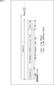
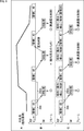
- FIG. 3 is a block diagram illustrating a configuration example of a light receiving unit 12.
- FIG. It is a figure which shows the required time when performing AD conversion by 10 bits with respect to a pixel signal in column ADC330. It is a figure which shows the required time when performing AD conversion by 1 bit with respect to a pixel signal in column ADC330.
- FIG. 6 is a timing chart in the case of using 1-bit AD conversion for saturation detection and performing exposure control based on the detection result.
- FIG. 6 is a timing chart when 1-bit AD conversion is used for saturation detection and light emission control is performed based on the detection result.
- FIG. 6 is a diagram for explaining a cooperative operation between a TOF sensor 10 and an HDR (High Dynamic Range) TOF sensor 600. It is a timing chart in the case of using 1-bit AD conversion for saturation detection and controlling the HDR-TOF sensor 600 based on the detection result.
- FIG. 5 is a diagram for explaining a cooperative operation between a TOF sensor 10 and a lid sensor 700.
- FIG. 5 is a diagram for explaining a cooperative operation between a TOF sensor 10 and a lid sensor 700.
- FIG. 6 is a diagram for explaining a first cooperative operation of 1-bit high-speed ranging and 10-bit high-precision ranging in the TOF sensor 10;
- FIG. 6 is a diagram for explaining a first cooperative operation of 1-bit high-speed ranging and 10-bit high-precision ranging in the TOF sensor 10;
- FIG. It is a figure for demonstrating the 2nd cooperation operation
- FIG. 3 is a block diagram illustrating a second configuration example of the TOF sensor 10.
- FIG. 4 is a block diagram illustrating a third configuration example of the TOF sensor 10.
- FIG. 7 is a block diagram illustrating a fourth configuration example of the TOF sensor 10.
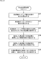
- FIG. It is a figure which shows the example of a light emission frequency state. It is a flowchart explaining the 1st light emission frequency Fmod change process. It is a flowchart explaining the 2nd light emission frequency Fmod change process. It is a flowchart explaining the 3rd light emission frequency Fmod change process.
- 6 is a block diagram illustrating a fifth configuration example of the TOF sensor 10.
- FIG. 10 is a block diagram illustrating a sixth configuration example of the TOF sensor 10.
- FIG. It is a figure which shows the outline
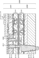
- FIG. 12 is a cross-sectional view illustrating a first configuration example of a stacked solid-state imaging device 23020.
- FIG. FIG. 11 is a cross-sectional view illustrating a second configuration example of a stacked solid-state imaging device 23020. It is sectional drawing which shows the 3rd structural example of the lamination type solid-state imaging device 23020.
- FIG. 12 is a cross-sectional view illustrating another configuration example of a stacked solid-state imaging device to which the technology according to the present disclosure can be applied. It is a block diagram which shows an example of a schematic structure of a vehicle control system. It is explanatory drawing which shows an example of the installation position of a vehicle exterior information detection part and an imaging part.
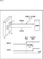
- FIG. 1 is a diagram illustrating an overview of an embodiment of a TOF sensor to which the present disclosure is applied.
- the TOF sensor 10 has a light emitting unit 11 and a light receiving unit 12, and measures the distance to the object by the TOF method.
- the light emitting unit 11 emits irradiation light such as predetermined modulated light such as pulsed light applied to the object.
- the light receiving unit 12 receives the reflected light reflected from the object by the irradiated light.
- the TOF sensor 10 obtains a time (hereinafter also referred to as reflection time) ⁇ t from the emission of the irradiation light at the light emitting unit 11 to the reception of the reflected light at the light receiving unit 12, and based on the above-described equation (1). Calculate the distance L to the object.
- the distance L to the object can be obtained by obtaining the reflection time ⁇ t.
- the first calculation method and the second calculation are used. There is a method.
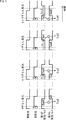
- FIG. 2 is a diagram for explaining the principle of the first calculation method of the reflection time ⁇ t.
- pulse light having a predetermined pulse width Tp is employed as the irradiation light.
- the TOF sensor receives the reflected light of the irradiated light (the light reflected by the target object) after a lapse of the reflection time ⁇ t corresponding to the distance L to the target object after the irradiated light is emitted.
- a pulse having the same pulse width and the same phase as the pulse light as the irradiation light is referred to as a first light reception pulse.
- a pulse having the same pulse width as that of the pulsed light as the irradiation light and having a phase shifted by the same width as the pulse width Tp of the pulsed light is referred to as a second received light pulse.
- reflected light is received in each of the period of the first light reception pulse (H (High) level) and the period of the second light reception pulse.
- the charge amount (received light amount) of the reflected light received during the period of the first light receiving pulse is expressed as Q1
- the charge amount of the reflected light received during the period of the second light receiving pulse is expressed as Q2.
- the reflection time ⁇ t can be obtained according to the following equation (2).
- ⁇ t Tp ⁇ Q2 / (Q1 + Q2) (2)
- the reflection time ⁇ t is proportional to the charge amount Q2. Therefore, when the distance L to the object is a short distance, the charge amount Q2 is small, and when the distance L to the object is a long distance, the charge amount Q2 is large.
- FIG. 2A shows irradiation light, reflected light, charge amount Q1 in the first light reception pulse, and charge amount Q2 in the second light reception pulse when the distance L to the object is a short distance
- B of FIG. 2 represents irradiation light, reflected light, the charge amount Q1 in the first light reception pulse, and the charge amount Q2 in the second light reception pulse when the distance L to the object is a long distance.
- the ambient light is received in addition to the reflected light during the period of the first and second light receiving pulses, the ambient light is calculated in calculating the reflection time ⁇ t (and the distance L). It is necessary to cancel the charge amount.
- the description of the cancellation of the amount of charge of the ambient light is omitted.
- FIG. 3 is a diagram for explaining the principle of the second calculation method of the reflection time ⁇ t.
- emission of pulsed light as irradiation light is performed a plurality of times, for example, four times.
- reflected light is received by shifting the first and second light-receiving pulses by ⁇ [rad] from the case of the first calculation method.
- the phase of the pulse width Tp of the pulsed light as the irradiation light is ⁇ [rad].
- the charge amount of the reflected light received during the period of the first light reception pulse in the ⁇ -shifted light reception is expressed as TapA
- the charge amount of the reflected light received during the period of the second light reception pulse is expressed as TapB. I will decide.
- the difference TapA-TapB between the charge amounts TapA and TapB obtained by shifting light by 0 is represented as a difference signal Sig1.
- the difference TapA-TapB between the charge amounts TapA and TapB obtained by ⁇ / 2 shifted light reception, ⁇ shifted light reception, and 3 ⁇ / 2 shifted light reception are represented as difference signals Sig2, Sig3, and Sig4, respectively. I will decide.
- phase difference ⁇ between the irradiated light and the reflected light can be obtained according to the following equation (3).
- ⁇ arctan ((Sig2-Sig4) / (Sig1-Sig3)) (3)
- phase difference ⁇ and the reflection time ⁇ t have a one-to-one correspondence, and the reflection time ⁇ t can be obtained according to the following equation (4) based on the phase difference ⁇ .
- ⁇ t Tp ⁇ ⁇ / ⁇ (4)
- the present disclosure can be applied to any of the first and second calculation methods described above, but hereinafter, the second calculation method of the first and second calculation methods will be described as an example.
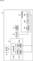
- FIG. 4 is a block diagram showing a first configuration example of the TOF sensor 10 shown in FIG.
- the first configuration example includes a light emitting unit 11, a light receiving unit 12, a distance calculating unit 51, and a control unit 53.
- the light emitting unit 11 is configured by, for example, an LED (Light Emitting Diode) or the like, and the target object is irradiated with light flashed in synchronization with the light emission frequency Fmod (including phase information) in accordance with control from the control unit 53. Irradiate in a possible direction.
- LED Light Emitting Diode
- Fmod including phase information
- the light receiving unit 12 includes the effective pixel unit 30 and the dummy pixel unit 40, and receives the reflected light from the object of the irradiation light emitted by the light emitting unit 11 according to the control from the control unit 53.
- a detailed configuration example of the light receiving unit 12 will be described later with reference to FIG.
- the effective pixel unit 30 includes a plurality of pixels 31, and the dummy pixel unit 40 includes a plurality of pixels 41.
- the pixels 31 and 41 are composed of, for example, a PD (photodiode) or the like, receive light incident thereon, and generate charges corresponding to the amount of light.
- a PD photodiode
- the pixel 31 receives the reflected light of the irradiation light emitted by the light emitting unit 11 according to the control of the control unit 53, and charges corresponding to the reflected light, that is, for example, the first described in FIG.
- the charge amount TapA of the reflected light received during the period of one light reception pulse and the charge amount TapB of the reflected light received during the period of the second light reception pulse are generated and supplied to the distance calculation unit 51.
- the pixel 41 is shielded from light, for example, and functions as a so-called OPB (Optical Black) pixel.
- OPB Optical Black
- the pixel 31 that constitutes the effective pixel unit 30 and the pixel 41 that constitutes the dummy pixel unit 40 are arranged in separate areas in order to avoid making the diagram complicated.
- the pixels 41 can be arranged so as to be mixed in the pixels 31, for example.
- the distance calculation unit 51 calculates the phase difference ⁇ using the charge amount of the charge from the pixel 31, for example, as described in FIG. 3, and based on the reflection time ⁇ t obtained from the phase difference ⁇ , the target Calculate the distance L to the object.
- the distance calculation unit 51 calculates a distance L for each pixel 31 constituting the effective pixel unit 30, and outputs a distance image having the pixel value as the distance L (a value corresponding to the distance L) as distance information. .
- the control unit 53 controls the emission of irradiation light by the light emitting unit 11 and the reception of reflected light by the pixels 31 of the light receiving unit 12.
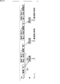
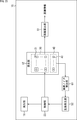
- FIG. 5 is a block diagram illustrating a configuration example of the light receiving unit 12.
- the light receiving unit 12 is configured in substantially the same manner as a solid-state imaging device such as a CMOS image sensor employing a column parallel ADC (Analog Digital Converter).
- a solid-state imaging device such as a CMOS image sensor employing a column parallel ADC (Analog Digital Converter).
- the light receiving unit 12 includes a pixel unit 101, a horizontal transfer scanning circuit 103, a vertical scanning circuit 105, a DAC (Digital Analog Converter) 310, a counter control unit 320, and a column parallel ADC 330.
- the column parallel ADC 330 is referred to as a column ADC 330.
- the pixel unit 101 corresponds to the effective pixel unit 30 and the dummy pixel unit 40 of FIG. 4, and is configured by arranging unit pixels 121 including PDs and various types of pixels Tr. (Transistors) in a matrix (matrix). .
- the unit pixel 121 corresponds to the pixels 31 and 41 in FIG.
- pixel drive lines (not shown) are formed for each row in a matrix-like pixel arrangement along the horizontal direction in the figure (pixel arrangement direction of the pixel row), and vertical signal lines are provided for each column.
- 122-1 to 122-N are formed along the vertical direction in the drawing (pixel arrangement direction of the pixel column).
- the vertical signal lines 122-1 to 122 -N are simply referred to as the vertical signal lines 122 when it is not necessary to distinguish them individually. The same description is applied to other parts.
- the vertical scanning circuit 105 is configured by a shift register, an address decoder, or the like, and is a pixel driving unit that drives each pixel of the pixel unit 101 at the same time or in units of rows.
- the vertical scanning circuit 105 is configured to have a readout scanning system and a sweep scanning system, or batch sweep and batch transfer, although illustration of the specific configuration is omitted.
- a pixel signal (voltage signal VSL) output from each unit pixel 121 in the pixel row selectively scanned by the vertical scanning circuit 105 is supplied to the column ADCs 330-1 to 330 through the vertical signal lines 122-1 to 122-N. -N supplied.
- the column ADC 330 performs AD conversion by performing predetermined signal processing on the pixel signal output from each unit pixel in the selected row through the vertical signal line 122 for each pixel column of the pixel unit 101, and is AD converted.
- the obtained pixel signal is supplied to the horizontal transfer scanning circuit 103.
- the horizontal transfer scanning circuit 103 includes a shift register, an address decoder, and the like, and sequentially selects unit circuits corresponding to the pixel columns of the columns ASDC 330-1 to 330-N. By the selective scanning by the horizontal transfer scanning circuit 103, the pixel signals AD-converted by the column ADC 330 are sequentially output to the distance calculation unit 51 in the subsequent stage.
- the DAC 310 includes a Vslop 311, a Vcons 312, and a switch 313.
- the counter control unit 320 includes a 10 bit / count 321, a 1 bit / count 322, and a switch 323.
- the column ADC 330 includes a comparator 331 and a counter 332, and performs AD conversion on the pixel signal from the unit pixel 121 supplied via the vertical signal line 122 with two or more different bit numbers (that is, accuracy). be able to.
- the column ADC 330 performs AD conversion on the pixel signal with an accuracy of 10 bits or 1 bit.
- these numbers of bits are merely examples, and are not limited to these. Note that AD conversion performed with 1-bit accuracy can be regarded as first AD conversion in one aspect of the present disclosure, and AD conversion performed with 10-bit accuracy is regarded as second AD conversion in one aspect of the present disclosure. be able to.
- the column ADC 330 performs AD conversion with 10-bit accuracy. Conversely, when the TOF sensor 10 performs distance measurement with low accuracy, the column ADC 330 performs AD conversion with 1-bit accuracy.
- the case where the TOF sensor 10 performs distance measurement with low accuracy means, for example, that there is no need to accurately determine the distance to the target object, and that no object is present up to a predetermined distance. This refers to the case where it can be detected.
- the switch 313 of the DAC 310 is connected to the Vslop 311 side. Further, the switch 323 of the counter control unit 320 is connected to the 10-bit / count 321 side (both are in a state opposite to the state shown in FIG. 5).
- the comparator 331 of the column ADC 330 is supplied with the reference voltage Vramp that changes in a slope shape generated by the Vslop 311 of the DAC 310.
- the counter 332 of the column ADC 330 is supplied with a control signal instructing to perform AD conversion at 10 bits from the 10 bits / count 321 of the counter controller 320.
- the reference voltage Vramp and the voltage signal VSL are compared in the comparator 331, and the comparator 331 outputs 1 as the output signal VCO while the reference voltage Vramp is larger than the voltage signal VSL.
- the counting operation of the counter 332 is stopped at this falling edge.
- the count value VCNT has a one-to-one relationship with the voltage width obtained by sweeping the reference voltage Vramp.
- the count value VCNT is supplied to the horizontal transfer scanning circuit 103 at the subsequent stage as a result of AD conversion of the pixel signal with 10 bits.
- the switch 313 of the DAC 301 is connected to the Vcons 312 side. Further, the switch 323 of the counter control unit 320 is connected to the 1 bit / count 322 side (both are shown in FIG. 5).
- the constant voltage Vcons generated by the Vcons 312 of the DAC 310 is supplied to the comparator 331 of the column ADC 330.
- the counter 332 of each column ADC 330 is supplied with a control signal instructing to perform AD conversion at 1 bit from 1 bit count 321 of the counter control unit 320.
- the comparator 331 compares the constant voltage Vcons with the voltage signal Vsl, and the comparator 331 outputs 1 as the output signal VCO while the constant voltage Vcons is larger than the voltage signal VSL. Then, at the timing when the constant voltage Vcons falls below the voltage signal VSL, 0 is output as the output signal VCO of the comparator 331. Then, triggered by the output signal VCO of the comparator 331 being inverted from 1 to 0 as a trigger, the digital code generated by the 1bit1count 322 in response to the inverted output signal of the comparator 331 (for example, a sum 1 greater than the reference voltage) If it is smaller, 0) is latched to the counter 332 (latch unit). This digital code is supplied to the horizontal transfer scanning circuit 103 at the subsequent stage as a result of AD conversion of the pixel signal by 1 bit.
- the time required for one ⁇ -shifted light reception includes a charge accumulation time (integration) in the unit pixel 121, a time required for AD conversion (RO), and an interval until the next ⁇ -shifted light reception (dead time).
- FIG. 6 shows a case where the column ADC 330 performs AD conversion on the pixel signal with 10-bit accuracy.
- the accumulation time is 0.5 [ms]
- the time required for 10-bit AD conversion is 2 [ms]
- the interval until the next ⁇ -shifted light reception requires a total of 2.6 [ms]. Therefore, one frame (time required for four times of ⁇ -shifted light reception) in the second calculation method of the reflection time ⁇ t described above is 10.4 [ms]
- the frame rate is 100 fps.
- the AD conversion performed on the pixel signal by the column ADC 330 with a precision of 10 bits (performs a high precision operation) and the distance measurement with a high precision based on the result is referred to as a 10 bit high precision distance measurement.
- FIG. 7 shows a case where the column ADC 330 performs AD conversion on the pixel signal with 1-bit accuracy.
- the accumulation time is 0.5 [ms]
- the time required for 1-bit AD conversion is 0.2 [ms]
- the interval until the next ⁇ -shifted light reception is 0.1 [ms] for a total of 0.8 [ms ] Is required.
- one frame (time required for four times of ⁇ -shifted light reception) in the second calculation method of the reflection time ⁇ t described above is 3.2 [ms]
- the frame rate is 313 fps.
- the AD conversion performed on the pixel signal by the column ADC 330 with 1-bit accuracy performs high-speed operation
- the distance measurement is performed with low accuracy based on the result is referred to as 1-bit high-speed distance measurement.
- the 1-bit high-speed distance measurement can significantly increase the speed compared to the 10-bit high-precision distance measurement.
- 1-bit high-speed ranging is used to detect the presence of an object within a predetermined distance or to detect that the light receiving unit 12 is saturated due to disturbance light or the like. Etc. can be used.
- the configuration example of the light receiving unit 12 illustrated in FIG. 5 can be formed as a stacked semiconductor device described later with reference to FIGS. 31 to 34.
- the components shown in FIG. 5 can be distributed and arranged on a plurality of stacked substrates.
- the pixel unit 101 may be arranged on the uppermost substrate and the other components may be arranged on the lower substrate.
- an ADC column ADC 330
- an ADC may be provided for every several pixels or ultimately for each unit pixel 121. Good. In that case, 1-bit high-speed ranging and 10-bit high-precision ranging can be further accelerated.
- 1-bit high-speed ranging For example, 1 greater than the reference voltage, 0 if smaller
- 1-bit digital code for example, 1 greater than the reference voltage, 0 if smaller
- FIG. 8 shows a timing chart when 1-bit high-speed ranging is used for saturation detection and exposure control of the light receiving unit 12 is performed based on the detection result.
- FIG. 8 has shown the change of the disturbance light which can become a factor of the saturation of the light-receiving part 12.
- FIG. FIG. 8B shows a case where 1-bit high-speed ranging is not used for saturation detection
- AD in the figure means execution of 10-bit AD conversion for 10-bit high-precision ranging.
- C in FIG. 8 shows a case where 1-bit high-speed ranging is used for saturation detection.
- AD in the figure means execution of 10-bit AD conversion for 10-bit high-precision ranging, and saturation detection in the figure.
- 10-bit AD conversion is performed as HW (hardware) processing.
- SW software
- a distance measurement calculation is performed by the processing, and an image for each frame (an image in which the pixel value of each pixel represents a distance or the like) is generated using the result.
- exposure control is performed when saturation of the light receiving unit 12 is detected based on the generated image.
- 10-bit AD conversion per frame requires about 3 [ms] including the charge accumulation time, and 30 [ms] for the SW processing for performing distance measurement and image generation. It takes a degree.
- FIG. 9 shows a timing chart when 1-bit high-speed ranging is used for saturation detection and light emission control of the light emitting unit 11 is performed based on the detection result.
- AD in the figure means execution of 10-bit AD conversion for 10-bit high-precision distance measurement
- saturation detection in the figure means execution of 1-bit high-speed distance measurement, that is, execution of 1-bit AD conversion.
- 1-bit high-speed processing is performed as HW processing during a period in which 10-bit AD conversion is not performed as HW processing, that is, during SW processing in the case of B in FIG. Saturation detection using distance measurement (1-bit AD conversion) is performed, and light emission control is performed using the result.
- the HDR TOF sensor can be regarded as another electronic device according to one aspect of the present disclosure.
- FIG. 10 and 11 are diagrams for explaining the cooperative operation between the TOF sensor 10 and the HDR-TOF sensor.
- a of FIG. 11 has shown the change of the disturbance light which can become a factor of the saturation of the light-receiving part 12.
- FIG. B of FIG. 11 shows the timing of saturation detection by 1-bit high-speed ranging by the TOF sensor 10 and the control timing of the HDR-TOF sensor based on the result.
- the HDR-TOF sensor performs imaging with a certain short exposure time (for example, 0.01 [ms], hereinafter referred to as short accumulation), and subsequently, a longer exposure time (for example, 1 [ms]). (Hereinafter referred to as long accumulation), and by synthesizing images taken with short accumulation and images taken with long accumulation, it is possible to generate an image with a high dynamic range wider than the normal dynamic range or calculate the distance. Point to.
- a certain short exposure time for example, 0.01 [ms]
- a longer exposure time for example, 1 [ms]
- the TOF sensor 10 performs saturation detection by performing 1-bit high-speed ranging when the HDR-TOF sensor 600 performs imaging with a short accumulation, and at the same time, the saturation detection result is converted into the HDR-TOF.
- the sensor 600 is notified.
- the long accumulation imaging that is scheduled to be performed after the short accumulation imaging is stopped. In this case, it is possible to promptly output short accumulation imaging without waiting for the time required for long accumulation imaging and synthesis.
- the HDR-TOF sensor 600 When the HDR-TOF sensor 600 has the same function as the TOF sensor 10, the HDR-TOF sensor 600 alone uses 1-bit high-speed ranging for saturation detection, and controls its own HDR function based on the detection result. It may be. That is, the HDR-TOF sensor 600 is scheduled to perform 1-bit high-speed ranging to detect saturation before performing short-accumulation imaging, and to perform short-accumulation imaging when saturation is detected. Try to stop long accumulation imaging. In this case, it is possible to promptly output short accumulation imaging without waiting for the time required for long accumulation imaging and synthesis.
- the lidar sensor can be regarded as another electronic device according to one aspect of the present disclosure.
- the lidar sensor measures the distance to the object by irradiating the object with laser light emitted in a pulsed manner and measuring the scattered light.
- the Lidar sensor can measure the distance with higher accuracy than the TOF sensor 10.
- an image obtained compared to the TOF sensor 10 (the pixel value of each pixel represents a distance).
- the scanning interval of the laser beam becomes wider as the resolution of the image or the like becomes lower and becomes farther away.
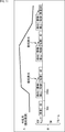
- FIG. 12 and 13 are diagrams for explaining the cooperative operation between the TOF sensor 10 and the lidar sensor 700.
- FIG. 12 and 13 are diagrams for explaining the cooperative operation between the TOF sensor 10 and the lidar sensor 700.
- the TOF sensor 10 and the lidar sensor 700 are mounted on the same vehicle (automobile or the like), and first, 1-bit AD conversion is performed by the column ADC 330 in the light receiving unit 12 of the TOF sensor 10. As shown by a broken line in FIG. 13A, the entire angle of view of the TOF sensor 10 is measured at high speed and with low accuracy. In practice, a region where some object is present up to a predetermined distance is detected.
- the TOF sensor 10 can detect a region where a certain object is present up to a predetermined distance (in the case of FIG. 13A, a humanoid region) in the entire angle of view.
- the TOF sensor 10 notifies the detection result to the lidar sensor 700.
- the lidar sensor 700 that has received the notification of the detection result from the TOF sensor 10 includes a relatively narrow area including an area where some object notified from the TOF sensor 10 exists (in the case of A in FIG. 13, a humanoid area).
- the distance to the object is measured with high accuracy by setting the scan range of the laser beam (indicated by a broken line in FIG. 13B).
- the lidar sensor 700 since the scan range of the laser beam by the lidar sensor 700 is limited to a relatively narrow region, the lidar sensor 700 has a scan interval even at a long distance compared to the case where the entire view angle is the scan range. Can be suppressed, and a high-resolution image (such as an image in which the pixel value of each pixel represents a distance) can be output.
- the TOF sensor 10 can perform low-precision distance measurement by 1-bit high-speed distance measurement and high-precision distance measurement by 10-bit high-precision distance measurement.
- 1-bit high-speed ranging can be executed at high speed and with low power consumption compared to 10-bit high-precision ranging. Therefore, in the first cooperative operation, the TOF sensor 10 is operated using such characteristics.
- FIG. 14 and FIG. 15 are diagrams for explaining a first cooperative operation between 1-bit high-speed ranging and 10-bit high-precision ranging in the TOF sensor 10.
- the column ADC 330 in the light receiving unit 12 of the TOF sensor 10 performs 1-bit AD conversion so that the entire angle of view of the TOF sensor 10 is targeted as shown by a broken line in FIG. Ranging is performed at high speed and with low accuracy as an object detection angle of view. In practice, a region where some object is present up to a predetermined distance is detected. While performing 1-bit AD conversion, the power consumption of the entire TOF sensor 10 can be suppressed.
- the TOF sensor 10 When an area where some object exists within a predetermined distance can be detected, the TOF sensor 10 then detects a relatively narrow area including the area (in the case of FIG. 15A, a humanoid area).
- the distance to the target is measured with high accuracy by performing 10-bit AD conversion (shown by a broken line in FIG. 15B) as the detection angle of view of the target.
- 10-bit AD conversion shown by a broken line in FIG. 15B
- an image (such as an image in which the pixel value of each pixel represents a distance) can be obtained more quickly than when the entire image is set as the detection angle of view. it can.
- the TOF sensor 10 can perform 1-bit high-speed ranging and 10-bit high accuracy.
- 10-bit high-precision distance measurement if the motion blur (blur) increases due to the movement of the object, it is difficult to perform distance measurement with high precision.
- 1-bit high-speed distance measurement even if motion blur occurs due to the movement of the object, the influence on distance measurement performed with low accuracy is relatively small. Therefore, in the second cooperative operation, the TOF sensor 10 is operated using such characteristics.
- FIGS. 16 and 17 are diagrams for explaining a second cooperative operation of the 1-bit high-speed ranging and the 10-bit high-precision ranging in the TOF sensor 10.
- the TOF sensor 10 performs 10-bit high-precision distance measurement. Then, as shown in FIG. 17A, when a motion occurs in the object and the motion bra exceeds a predetermined threshold, the TOF sensor 10 then performs 10-bit high accuracy as shown in FIG. Switch from ranging to 1-bit high-speed ranging.
- the light emission frequency Fmod (light blinking frequency) of the light emitting unit 11 is started from a predetermined low value, and the object is present at a predetermined medium and long distance. Is detected, the emission frequency Fmod is increased stepwise to a high value to measure the distance to the object more accurately.
- the Vision sensor can be regarded as another electronic device according to one aspect of the present disclosure.
- the Vision sensor can capture moving images at a very high frame rate (for example, 300 fps) compared to the frame rate of general video cameras (about 30 fps).
- FIG. 18 is a diagram for explaining the cooperative operation between the TOF sensor 10 and the Vision sensor 800.
- the TOF sensor 10 and the Vision sensor 800 are mounted on the same vehicle (automobile or the like), and the TOF sensor 10 performs 1-bit AD conversion and operates at 300 fps.
- the Vision sensor 800 is operated at 300 fps, a moving image with a very high frame rate and an output image from the TOF sensor 10 synchronized with the moving image (the object exists between the pixel value of each pixel up to a predetermined distance) An image showing whether or not to do so can be obtained.
- the Vision sensor 800 when the Vision sensor 800 is operated first and it is detected that an object is present in the moving image picked up by the Vision sensor 800, 1-bit high-speed measurement is performed with the TOF sensor 10 as a trigger.
- the distance may be started, or 10-bit high-precision distance measurement may be started.
- the detection result of one of the TOF sensor 10 and the Vision sensor 800 is used as a trigger for starting the other operation, an object moving at high speed can be handled. In this case, while waiting for one detection result, the other can reduce power consumption.
- a certain TOF sensor receives not only the reflected light of the emitted light emitted by itself but also the emitted light emitted by other TOF sensors and the reflected light thereof. Interference may occur. If interference occurs in the TOF sensor, the accuracy of distance measurement will decrease, so it is necessary to take measures against interference in the TOF sensor so that the accuracy of distance measurement can be maintained.
- FIG. 19 is a timing chart illustrating an example of distance measurement when the TOF sensor obtains the reflection time ⁇ t by the above-described second calculation method.
- the TOF sensor calculates the distance L in units of frames, with the period for calculating the distance L to the object as a frame.
- the frame length is, for example, 33 [ms].
- the frame includes a plurality of subframes sub that are periods in which the irradiation light is emitted.
- the length of the subframe is, for example, 0.2 [ms].
- the frame includes, for example, four subframes sub, and the four subframes sub are arranged from the head of the frame at a predetermined constant interval sd.
- the time of light emission and ⁇ -shifted light reception for one time (for example, the time corresponding to the phase of 2 ⁇ ) is set to 100 [ns], for example, the time of light emission and ⁇ -shifted light reception For example, 2000 times or more.
- the total amount of the charges of the reflected light received a plurality of times such as 2000 times is used.
- the subframe sub of one frame with the TOF sensor and the subframe of another TOF sensor When an overlap with sub occurs, the overlap of the subframe sub continues with other TOF sensors in the subsequent frames of the TOF sensor.
- the TOF sensor In the period in which the subframes sub are overlapped, the TOF sensor generates interference that receives irradiation light emitted by other TOF sensors in addition to the irradiation light emitted by itself.
- Interference affects the charge amount TapA (or Q1) during the first light-receiving pulse period and the charge amount TapB (or Q2) during the second light-receiving pulse period, and causes a decrease in distance measurement accuracy.
- FIG. 20 is a timing chart for explaining an example of distance measurement in the case where the TOF sensor that has taken measures against interference obtains the reflection time ⁇ t by the second calculation method.
- each frame when a plurality of subframes sub are arranged from the head of the frame at a constant interval sd, subframes are exchanged with other TOF sensors.
- subframe sub overlap occurs, sub frame sub overlap also continues in subsequent frames, and interference continues.
- the timing of the first subframe sub is different between the first frame that is a certain frame and the second frame that follows the first frame, and the subframes are different from each other.
- the emission of the irradiation light (and the reception of the reflected light of the irradiation light) is controlled so that the interval sd is constant.
- the TOF sensor that has performed the interference countermeasures arranges a plurality of subframes sub at a constant interval sd from the beginning of the frame in the first frame, as in the case of FIG. 19.
- the emission of irradiation light is controlled.
- the TOF sensor that has taken measures against interference causes the irradiation light to be arranged so that a plurality of subframes sub are arranged at a constant interval sd from the timing when a predetermined time has elapsed from the beginning of the frame. Control light emission.
- the timing at which the top subframe sub of a plurality of subframes sub in the frame starts is also referred to as head timing.
- the first frame which is a frame
- the second frame following the first frame the interval sd between subframes is kept constant (fixed), and the head
- the emission of irradiation light is controlled so as to change only the timing.
- the emission of irradiation light is controlled so that the first frame and the second frame following the first frame have different start timings and the intervals between subframes are constant. Thus, interference can be suppressed.
- the subframe sub does not overlap with other TOF sensors, and interference does not occur.
- the head timing can be changed, for example, according to a predetermined pattern or can be changed randomly. Rather than changing the start timing according to a predetermined pattern, the probability of suppressing interference can be improved by changing it randomly.
- the start timing (subframe position) of the subframe is changed randomly in units of subframes rather than the start timing is changed randomly in units of frames.
- the probability of suppressing interference can be improved.
- the process and circuit for controlling the emission of emitted light is less than in the case where the start timing of subframes is changed randomly in units of subframes. As a result, interference can be easily suppressed.
- the power consumption can be suppressed compared to when the start timing of subframes is changed randomly in units of subframes.
- FIG. 21 shows a case where the start timing is randomly changed in units of frames (A in FIG. 21), and a case where the start timing of the subframe is changed randomly in units of subframes (B in FIG. 21). It is a figure explaining the example of the power consumption of.
- a method of randomly changing (shifting) the start timing in units of frames for example, a method of controlling the start timing based on a random number can be employed.
- a method of randomly changing (shifting) the start timing of subframes in units of subframes a method of controlling the start timing of subframes based on random numbers can be employed.
- FIG. 21A shows an example of the state of random number generation processing when the head timing is changed randomly in units of frames.
- the random number generation process can be in an active state for a predetermined period immediately before the start of a frame, and can be in a standby state for other periods.
- the power consumption when the random number generation process is in the active state is 50 [mW]
- the power consumption when the random number generation process is in the standby state is 0.1 [mW].
- FIG. 21B shows an example of the state of random number generation processing when the start timing of a subframe is randomly changed in units of subframes.
- the random number generation processing is made active only for a predetermined period immediately before the start of the frame, and in other cases the standby state can be set for the other period.
- the standby state can be set for the other period.
- FIG. 22 is a block diagram illustrating a configuration example (second configuration example) of the TOF sensor 10 that has taken measures against interference.
- the second configuration example is obtained by adding a random number generator 52 to the first configuration example (configuration example in which interference countermeasures are not taken) shown in FIG. 4, and other common configurations. Since the same reference numerals are given to the elements, description thereof will be omitted as appropriate.
- the random number generation unit 52 generates a random number using, for example, a predetermined value as a seed of random numbers, and supplies the random number to the control unit 53.
- the control unit 53 in the second configuration example controls the emission of irradiation light by the light emitting unit 11 and the reception of reflected light by the pixels 31 of the light receiving unit 12.
- control unit 53 controls the emission of emitted light and the reception of reflected light based on the random number from the random number generation unit 52. Control the start timing to start. As a result, the head timing changes randomly in units of frames.
- the control unit 53 can control the active and standby of the random number generation unit 52 (random number generation processing) as shown in A of FIG.
- FIG. 23 is a block diagram showing another configuration example (third configuration example) of the TOF sensor 10 that has taken measures against interference.
- the third configuration example is obtained by adding a pixel noise detection unit 61 to the second configuration example shown in FIG. 22, and other common components are denoted by the same reference numerals. Therefore, the description is omitted as appropriate.
- the pixel noise detection unit 61 detects, for example, the charge amount of the pixel 41 which is an OPB pixel as pixel noise generated in the pixels 31 and 41 and supplies the detected noise to the random number generation unit 52.
- the pixel noise detection unit 61 can select the plurality of pixels 41 of the dummy pixel unit 40 in a specific order or an arbitrary order, and detect the charge amount of the selected pixel 41 as pixel noise.
- the random number generation unit 52 in the third configuration example generates a random number using the pixel noise supplied from the pixel noise detection unit 61 as a seed of random numbers.
- the pixel noise characteristics of the pixel 31 and the pixel 41 are (almost) random characteristics. Therefore, in the third configuration example in which random numbers are generated using pixel noise having such random characteristics as a seed, and the leading timing is controlled based on the random numbers, the second configuration example shown in FIG. Compared to the above, interference (possibility of occurrence) can be further suppressed.
- the distance measurement accuracy of the TOF sensor 10 is proportional to the product of the characteristics of the pixel 31 and the interference suppression characteristics.
- the TOF sensor 10 when the TOF sensor 10 generates a random number using pixel noise as a seed and controls the head timing based on the random number, the accuracy of distance measurement can be maintained at a (substantially) constant value. .
- interference is suppressed by performing at least one of frequency hopping of the light emission frequency Fmod (light blinking frequency) of the light emitting unit 11 and phase change. .
- the frequency hopping of the emission frequency Fmod is a method of spread spectrum, and refers to a process of switching the emission frequency Fmod at high speed according to a certain rule. Specifically, for example, it indicates a process of changing the emission frequency Fmod (for example, 60 [MHz]) before frequency hopping to 59.999 [MHz], 59.992 [MHz], or the like step by step.
- Frequency hopping of the emission frequency Fmod is effective for suppressing interference, but disadvantages include complicated processing and increased power consumption.
- the phase change of the light emission frequency Fmod refers to a process of shifting the phase of two values switched in synchronization with the light emission frequency Fmod (for example, 101010, 0 is turned off and 1 is turned on) by ⁇ [rad] and inverted to 010101. For example, it is assumed that the processing is executed randomly in subframe sub units.
- Changing the phase of the emission frequency Fmod is also effective for suppressing interference. Further, it can be executed without increasing the power consumption as in the case of frequency hopping. However, as a demerit, when the light emission frequency Fmod and the interference wave (light emission frequency Fmod of other TOF sensors) are almost the same, the effect of suppressing interference is reduced.
- the frequency hopping and phase change characteristics described above are considered and the frequency hopping and phase change are used properly according to the use case.
- phase change should be prioritized and frequency hopping should be avoided as much as possible.
- frequency hopping and phase change are executed so that interference can be suppressed more effectively.
- frequency hopping is repeatedly executed to search for the optimum light emission frequency Fmod, and then the phase is changed to reliably suppress interference with the jamming waves.
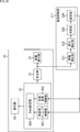
- FIG. 24 is a block diagram illustrating a fourth configuration example of the TOF sensor 10.
- the fourth configuration example is obtained by adding an interference suppression unit 511 to the outside of the first configuration example shown in FIG.
- symbol is attached
- the control unit 53 in the fourth configuration example includes a frequency hopping control unit 501, a phase change control unit 502, and an Fmod setting unit 503.
- the frequency hopping control unit 501 causes the Fmod setting unit 503 to perform frequency hopping of the light emission frequency Fmod according to the control from the interference suppression unit 511.
- the phase change control unit 502 causes the Fmod setting unit 503 to change the phase of the light emission frequency Fmod according to the control from the interference suppression unit 511.
- the Fmod setting unit 503 executes frequency hopping of the light emission frequency Fmod according to the control from the frequency hopping control unit 501. Further, the Fmod setting unit 503 executes the phase change of the light emission frequency Fmod according to the control from the phase change control unit 502.
- the interference suppression unit 511 includes a distance detection unit 521, a difference detection unit 522, a determination unit 523, and a setting unit 524.
- the distance detecting unit 521 Based on the pixel signal supplied from the light receiving unit 12 (same as the pixel signal output to the distance calculating unit 51), the distance detecting unit 521 has a distance to the object in units of frames as in the distance calculating unit 51. L is calculated and output to the difference detection unit 522.
- the distance detection unit 521 may be omitted, and the distance L to the object calculated by the distance calculation unit 51 may be supplied to the difference detection unit 522.
- the difference detection unit 522 calculates the variation in the distance L corresponding to each frame for a predetermined number of frames (for example, several hundred frames) calculated under the same light emission frequency state (light emission frequency Fmod and presence / absence of phase change). A difference representing the degree is detected and output to the determination unit 523.
- the difference described above is calculated by calculating the average value of the distance L corresponding to each frame for a predetermined number of frames as a reference value, and calculating the average value of the difference between the reference value and the distance L of each frame as a percentage. And so on.
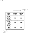
- FIG. 25 is a diagram showing an example of a light emission frequency state.
- a state a indicates a state where frequency hopping and phase change are not applied (not implemented).
- State b indicates a state where frequency hopping is not applied and phase change is applied (implemented).
- the state c indicates a state where frequency hopping is applied in one stage and phase change is not applied.
- State d indicates a state where frequency hopping is applied in one stage and phase change is applied.
- State e refers to a state where frequency hopping is applied in two stages and phase change is not applied.
- the state f indicates a state where frequency hopping is applied in two stages and phase change is applied.
- the value of the light emission frequency Fmod shown in FIG. 25 is merely an example, and is not limited to these.
- the determination unit 523 compares the differences detected under different light emission frequency conditions. For example, the difference detected in the state a in FIG. 25 is compared with the difference detected in the state b, or the difference detected in the state c is compared with the difference detected in the state e.
- the determination unit 523 outputs the comparison result to the setting unit 524.
- the setting unit 524 controls the frequency hopping control unit 501 and the phase change control unit 502 based on the determination result input from the determination unit 523.
- FIG. 26 is a flowchart for explaining the first light emission frequency Fmod changing process according to the fourth configuration example of the TOF sensor 10.
- the first light emission frequency Fmod changing process assumes a use case in the mobile field where power saving is required.
- the first light emission frequency Fmod change process is started when interference is suspected.
- step S11 the difference detection unit 522 of the interference suppression unit 511 maintains the current light emission frequency Fmod, and calculates a predetermined value calculated under a state in which no phase change is applied (for example, state a in FIG. 25). A difference representing the degree of variation in the distance L corresponding to each frame for the number of frames is detected and output to the determination unit 523.
- the control unit 53 controls the emission frequency state according to the control from the setting unit 524 so that the interference suppression unit 511 can obtain the pixel signal used to calculate the distance L corresponding to each frame for a predetermined number of frames. Are adjusted appropriately.
- step S12 the difference detection unit 522 maintains the current light emission frequency Fmod and outputs a predetermined number of frames calculated under the state where the phase change is applied (in this case, the state b in FIG. 25). A difference representing the degree of variation in the distance L corresponding to each frame is detected and output to the determination unit 523.
- step S ⁇ b> 13 the determination unit 523 has the effect of applying the phase change based on the difference calculated under the state where the phase change is not applied and the difference calculated under the state where the phase change is applied. It is determined whether or not there is.
- the difference calculated under the condition where the phase change is not applied is equal to or greater than the first threshold value for determining the presence / absence of interference, and is calculated under the condition where the phase change is applied. If the calculated difference is equal to or smaller than the second threshold value that is smaller than the first threshold value, it can be estimated that the state in which interference has occurred has changed to a state in which interference has been suppressed. Therefore, it is determined that there is an effect of applying the phase change. In this case, the process proceeds to step S14.
- the setting unit 524 controls the phase change control unit 502 of the control unit 53 to apply the phase change while maintaining the current light emission frequency Fmod.
- step S15 the setting unit 524 controls the frequency hopping control unit 501 of the control unit 53 so as to perform frequency hopping without applying the phase change while maintaining the light emission frequency Fmod.
- the first light emission frequency Fmod changing process described above it is possible to suppress the generated interference and maintain the accuracy of distance measurement.
- the phase change can be performed with priority and frequency hopping can be avoided as much as possible, an increase in power consumption that can be caused by performing frequency hopping can be suppressed.
- FIG. 27 is a flowchart for explaining the second light emission frequency Fmod changing process by the fourth configuration example of the TOF sensor 10.
- the second light emission frequency Fmod changing process assumes a use case in a vehicle or the like in which distance measurement with higher accuracy than power saving is required.
- the second light emission frequency Fmod changing process is started when interference is suspected.
- step S21 the difference detection unit 522 of the interference suppression unit 511 remains in the current emission frequency Fmod before performing frequency hopping, and does not apply a phase change (for example, state a in FIG. 25).
- the calculated difference indicating the degree of variation in the distance L corresponding to each predetermined number of frames is detected and output to the determination unit 523.
- the control unit 53 controls the emission frequency state according to the control from the setting unit 524 so that the interference suppression unit 511 can obtain the pixel signal used to calculate the distance L corresponding to each frame for a predetermined number of frames. Are adjusted appropriately.
- step S22 the difference detection unit 522 performs frequency hopping from the current light emission frequency Fmod, and calculates a predetermined frame calculated under a state where no phase change is applied (in this case, state c in FIG. 25). A difference indicating the degree of variation in the distance L corresponding to several frames is detected and output to the determination unit 523.
- step S23 the determination unit 523 compares the difference calculated in step S21 with the difference calculated in step S22, and notifies the setting unit 524 of the frequency having the smaller value.
- the setting unit 524 controls the frequency hopping control unit 501 of the control unit 53 according to the notification from the determination unit 523. That is, if the difference calculated in step S21 is smaller, control is performed so that frequency hopping is not performed, and if the difference calculated in step S22 is smaller, control is performed so that frequency hopping is performed.
- step S24 the difference detection unit 522 of the interference suppression unit 511 remains in the light emission frequency Fmod set in step S23 and does not apply the phase change (in this case, the state a or the state a in FIG. A difference representing the degree of variation in the distance L corresponding to each predetermined number of frames calculated under the state c) is detected and output to the determination unit 523. Since the process of step S24 is the same as the process of step S21 that has already been executed or the process of step S22, either of the process results may be used in accordance with the determination result of step S23.
- step S25 the difference detection unit 522 of the interference suppression unit 511 remains in the light emission frequency Fmod set in step S23 and is in a state where the phase change is applied (for example, state b or state d in FIG. 25).
- the difference indicating the degree of variation in the distance L corresponding to each frame for the predetermined number of frames calculated in step S is detected and output to the determination unit 523.
- step S26 the determination unit 523 compares the difference calculated in step S24 (phase change not applied) with the difference calculated in step S25 (phase change applied), and determines the smaller value.
- the determination result is notified to the setting unit 524.
- the setting unit 524 controls the phase change control unit 502 of the control unit 53 based on the determination result of the determination unit 523. That is, if the difference calculated in step S24 is smaller, control is performed so that the phase change is not applied, and if the difference calculated in step S25 is smaller, control is performed so that the phase change is applied.
- frequency hopping and phase change can be used together depending on the situation, so that interference can be further suppressed and the accuracy of distance measurement can be maintained.
- FIG. 28 is a flowchart for explaining the third light emission frequency Fmod changing process according to the fourth configuration example of the TOF sensor 10.
- the third light emission frequency Fmod changing process assumes a use case in an environment with many interference waves, for example. Steps S31 to S33 in the third light emission frequency Fmod change process are the same as steps S21 to S23 in the second light emission frequency Fmod change process shown in FIG.
- step S34 the determination unit 523 determines whether or not a desired accuracy is obtained as a result of the process in the previous step S33. If it is determined that the desired accuracy is not obtained, the process returns to step S32, and steps S32 and S34 are repeated. That is, frequency hopping is repeated. When the frequency hopping is repeated, the emission frequency Fmod gradually moves away from the frequency of the interference wave, so that interference can be further suppressed. Thereafter, when it is determined in step S34 that the desired accuracy is obtained, the process proceeds to step S35. Note that steps S35 to S37 are the same as steps S24 to S26 in the second light emission frequency Fmod changing process shown in FIG.
- frequency hopping can be repeated until a desired accuracy is obtained, and furthermore, phase change can be used together. It is possible to further suppress and maintain the accuracy of distance measurement.
- FIG. 29 is a block diagram illustrating a fifth configuration example of the TOF sensor 10.
- the interference suppression unit 511 provided outside in the fourth configuration example shown in FIG. 24 is provided inside the TOF sensor 10, and the interference detection unit 511 to the distance detection unit 521 are provided. Is omitted.
- symbol is attached
- the interference suppression unit 511 in the fifth configuration example includes a difference detection unit 522, a determination unit 523, and a setting unit 524.
- the difference detection unit 522 in the fifth configuration example has a predetermined value input from the light receiving unit 12 corresponding to each frame for a predetermined number of frames (for example, several hundred frames) under the same light emission frequency state. A difference indicating the degree of variation is detected and output to the determination unit 523.
- the difference detected by the difference detection unit 522 is used to determine the presence / absence and the degree of interference, and therefore does not necessarily represent the degree of variation in the distance L.
- the value supplied from the light receiving unit 12 to the difference detecting unit 522 in the fifth configuration example may be anything as long as it corresponds to each frame. For example, a charge amount generated in a pixel, a pixel signal before AD conversion corresponding to the charge amount, a pixel signal after AD conversion corresponding to the charge amount, or a charge amount TapA-charge amount TapB are adopted. Can do.
- the average value of the distance L corresponding to each frame for a predetermined number of frames is calculated as a reference value, and the distance between the reference value and each frame is calculated.
- the average value of the difference from L is calculated and expressed as a percentage or the like.
- FIG. 30 is a block diagram illustrating a sixth configuration example of the TOF sensor 10.
- the sixth configuration example is obtained by adding an interference suppression unit 551 to the first configuration example shown in FIG.
- symbol is attached
- the control unit 53 in the sixth configuration example includes a frequency hopping control unit 501, a phase change control unit 502, and an Fmod setting unit 503.
- the frequency hopping control unit 501, the phase change control unit 502, and the Fmod setting unit 503 are the same as those in the fourth configuration example shown in FIG.
- the interference suppression unit 551 includes a communication unit 552 and a setting unit 553.
- the communication unit 552 communicates the light emission frequency state with the communication unit 552 of another TOF sensor having the same configuration existing in the surroundings, and supplies the light emission frequency state of the other TOF sensor to the setting unit 553.
- the setting unit 553 controls the frequency hopping control unit 501 and the phase change control unit 502 so that interference does not occur based on the emission frequency state of another TOF sensor supplied from the communication unit 552.
- the interference with the TOF sensor existing in the surrounding area is prevented. It can be surely suppressed. Therefore, the accuracy of distance measurement can be maintained.
- FIG. 31 is a diagram illustrating an outline of a configuration example of a solid-state imaging device as an example of a stacked semiconductor device to which the technology according to the present disclosure can be applied.
- FIG. 31A shows a schematic configuration example of a non-stacked solid-state imaging device.
- the solid-state imaging device 23010 has one die (semiconductor substrate) 23011 as shown in FIG.
- the die 23011 is mounted with a pixel region 23012 in which pixels are arranged in an array, a control circuit 23013 for driving the pixel and other various controls, and a logic circuit 23014 for signal processing.
- the solid-state imaging device 23020 is configured as a single semiconductor chip in which two dies, a sensor die 23021 and a logic die 23024, are stacked and electrically connected.
- the pixel region 23012 and the control circuit 23013 are mounted on the sensor die 23021, and the logic circuit 23014 including a signal processing circuit for performing signal processing is mounted on the logic die 23024.
- the pixel region 23012 is mounted on the sensor die 23021, and the control circuit 23013 and the logic circuit 23014 are mounted on the logic die 23024.
- FIG. 32 is a cross-sectional view showing a first configuration example of a stacked solid-state imaging device 23020.
- a PD photodiode
- an FD floating diffusion
- a Tr MOS FET
- a Tr serving as a control circuit 23013, and the like constituting a pixel serving as a pixel region 23012 are formed.
- the sensor die 23021 is formed with a wiring layer 23101 having a plurality of layers, in this example, three layers of wiring 23110.
- the control circuit 23013 (which is the Tr) can be configured not on the sensor die 23021 but on the logic die 23024.
- a Tr constituting the logic circuit 23014 is formed. Further, the logic die 23024 is formed with a wiring layer 23161 having a plurality of layers 23170 in this example. In the logic die 23024, a connection hole 23171 having an insulating film 23172 formed on the inner wall surface is formed, and a connection conductor 23173 connected to the wiring 23170 and the like is embedded in the connection hole 23171.
- the sensor die 23021 and the logic die 23024 are bonded together so that the wiring layers 23101 and 23161 face each other, thereby forming a stacked solid-state imaging device 23020 in which the sensor die 23021 and the logic die 23024 are stacked.
- a film 23191 such as a protective film is formed on the surface where the sensor die 23021 and the logic die 23024 are bonded.
- connection hole 23111 is formed which penetrates the sensor die 23021 from the back side (side where light enters the PD) (upper side) of the sensor die 23021 to reach the uppermost wiring 23170 of the logic die 23024.
- a connection hole 23121 is formed in the sensor die 23021 in the vicinity of the connection hole 23111 so as to reach the first layer wiring 23110 from the back surface side of the sensor die 23021.
- An insulating film 23112 is formed on the inner wall surface of the connection hole 23111, and an insulating film 23122 is formed on the inner wall surface of the connection hole 23121.
- Connection conductors 23113 and 23123 are embedded in the connection holes 23111 and 23121, respectively.
- connection conductor 23113 and the connection conductor 23123 are electrically connected on the back side of the sensor die 23021, whereby the sensor die 23021 and the logic die 23024 are connected to the wiring layer 23101, the connection hole 23121, the connection hole 23111, and the wiring layer. Electrical connection is established via 23161.
- FIG. 33 is a cross-sectional view illustrating a second configuration example of the stacked solid-state imaging device 23020.
- the sensor die 23021 (the wiring layer 23101 (the wiring 23110)) and the logic die 23024 (the wiring layer 23161 (the wiring thereof) are formed by one connection hole 23211 formed in the sensor die 23021. 23170)) are electrically connected.
- connection hole 23211 is formed so as to penetrate the sensor die 23021 from the back side of the sensor die 23021 to reach the uppermost layer wiring 23170 of the logic die 23024 and to reach the uppermost layer wiring 23110 of the sensor die 23021. Is done.
- An insulating film 23212 is formed on the inner wall surface of the connection hole 23211, and a connection conductor 23213 is embedded in the connection hole 23211.
- the sensor die 23021 and the logic die 23024 are electrically connected by the two connection holes 23111 and 23121.
- the sensor die 23021 and the logic die 23024 are connected by the single connection hole 23211. Electrically connected.
- FIG. 34 is a cross-sectional view showing a third configuration example of the stacked solid-state imaging device 23020.
- the solid-state imaging device 23020 in FIG. 34 has a surface on which the sensor die 23021 and the logic die 23024 are bonded to each other in that a film 23191 such as a protective film is not formed on the surface on which the sensor die 23021 and the logic die 23024 are bonded. This is different from the case of FIG. 32 in which a film 23191 such as a protective film is formed.
- the solid-state imaging device 23020 in FIG. 34 is configured by superimposing the sensor die 23021 and the logic die 23024 so that the wirings 23110 and 23170 are in direct contact with each other, heating them while applying a required weight, and directly joining the wirings 23110 and 23170. Composed.
- FIG. 35 is a cross-sectional view illustrating another configuration example of the stacked solid-state imaging device to which the technology according to the present disclosure can be applied.
- the solid-state imaging device 23401 has a three-layer structure in which three dies of a sensor die 23411, a logic die 23412, and a memory die 23413 are stacked.
- the memory die 23413 includes, for example, a memory circuit that stores data temporarily required for signal processing performed by the logic die 23412.
- the logic die 23412 and the memory die 23413 are stacked in that order under the sensor die 23411. However, the logic die 23412 and the memory die 23413 are arranged in the reverse order, that is, in the order of the memory die 23413 and the logic die 23412. Can be laminated under 23411.
- the sensor die 23411 is formed with a PD serving as a photoelectric conversion portion of the pixel and a source / drain region of the pixel Tr.
- a gate electrode is formed around the PD via a gate insulating film, and a pixel Tr23421 and a pixel Tr23422 are formed by a source / drain region paired with the gate electrode.
- the pixel Tr23421 adjacent to the PD is the transfer Tr, and one of the pair of source / drain regions constituting the pixel Tr23421 is FD.
- an interlayer insulating film is formed in the sensor die 23411, and a connection hole is formed in the interlayer insulating film.
- a connection hole is formed in the connection hole, a pixel Tr23421 and a connection conductor 23431 connected to the pixel Tr23422 are formed.
- the sensor die 23411 is formed with a wiring layer 23433 having a plurality of layers of wirings 23432 connected to the respective connection conductors 23431.
- an aluminum pad 23434 serving as an electrode for external connection is formed in the lowermost layer of the wiring layer 23433 of the sensor die 23411.
- the aluminum pad 23434 is formed at a position closer to the bonding surface 23440 with the logic die 23412 than to the wiring 23432.
- the aluminum pad 23434 is used as one end of a wiring related to signal input / output with the outside.
- a contact 23441 used for electrical connection with the logic die 23412 is formed on the sensor die 23411.
- the contact 23441 is connected to the contact 23451 of the logic die 23412 and also to the aluminum pad 23442 of the sensor die 23411.
- a pad hole 23443 is formed so as to reach the aluminum pad 23442 from the back side (upper side) of the sensor die 23411.
- the technology according to the present disclosure can be formed as a stacked semiconductor device as described above.
- the technology (present disclosure) according to the present disclosure can be applied to various products.
- the technology according to the present disclosure is realized as a device that is mounted on any type of mobile body such as an automobile, an electric vehicle, a hybrid electric vehicle, a motorcycle, a bicycle, personal mobility, an airplane, a drone, a ship, and a robot. May be.
- FIG. 36 is a block diagram illustrating a schematic configuration example of a vehicle control system that is an example of a mobile control system to which the technology according to the present disclosure can be applied.
- the vehicle control system 12000 includes a plurality of electronic control units connected via a communication network 12001.
- the vehicle control system 12000 includes a drive system control unit 12010, a body system control unit 12020, an outside information detection unit 12030, an in-vehicle information detection unit 12040, and an integrated control unit 12050.
- a microcomputer 12051, an audio image output unit 12052, and an in-vehicle network I / F (interface) 12053 are illustrated.
- the drive system control unit 12010 controls the operation of the device related to the drive system of the vehicle according to various programs.
- the drive system control unit 12010 includes a driving force generator for generating a driving force of a vehicle such as an internal combustion engine or a driving motor, a driving force transmission mechanism for transmitting the driving force to wheels, and a steering angle of the vehicle. It functions as a control device such as a steering mechanism that adjusts and a braking device that generates a braking force of the vehicle.
- the body system control unit 12020 controls the operation of various devices mounted on the vehicle body according to various programs.
- the body system control unit 12020 functions as a keyless entry system, a smart key system, a power window device, or a control device for various lamps such as a headlamp, a back lamp, a brake lamp, a blinker, or a fog lamp.
- the body control unit 12020 can be input with radio waves transmitted from a portable device that substitutes for a key or signals from various switches.
- the body system control unit 12020 receives input of these radio waves or signals, and controls a door lock device, a power window device, a lamp, and the like of the vehicle.
- the vehicle outside information detection unit 12030 detects information outside the vehicle on which the vehicle control system 12000 is mounted.
- the imaging unit 12031 is connected to the vehicle exterior information detection unit 12030.
- the vehicle exterior information detection unit 12030 causes the imaging unit 12031 to capture an image outside the vehicle and receives the captured image.
- the vehicle outside information detection unit 12030 may perform an object detection process or a distance detection process such as a person, a car, an obstacle, a sign, or a character on a road surface based on the received image.
- the imaging unit 12031 is an optical sensor that receives light and outputs an electrical signal corresponding to the amount of received light.
- the imaging unit 12031 can output an electrical signal as an image, or can output it as distance measurement information. Further, the light received by the imaging unit 12031 may be visible light or invisible light such as infrared rays.
- the vehicle interior information detection unit 12040 detects vehicle interior information.
- a driver state detection unit 12041 that detects a driver's state is connected to the in-vehicle information detection unit 12040.
- the driver state detection unit 12041 includes, for example, a camera that images the driver, and the vehicle interior information detection unit 12040 determines the degree of fatigue or concentration of the driver based on the detection information input from the driver state detection unit 12041. It may be calculated or it may be determined whether the driver is asleep.
- the microcomputer 12051 calculates a control target value of the driving force generator, the steering mechanism, or the braking device based on the information inside / outside the vehicle acquired by the vehicle outside information detection unit 12030 or the vehicle interior information detection unit 12040, and the drive system control unit A control command can be output to 12010.
- the microcomputer 12051 realizes an ADAS (Advanced Driver Assistance System) function including vehicle collision avoidance or impact mitigation, following traveling based on inter-vehicle distance, vehicle speed maintaining traveling, vehicle collision warning, or vehicle lane departure warning, etc. It is possible to perform cooperative control for the purpose.
- ADAS Advanced Driver Assistance System
- the microcomputer 12051 controls the driving force generator, the steering mechanism, the braking device, and the like based on the information around the vehicle acquired by the vehicle exterior information detection unit 12030 or the vehicle interior information detection unit 12040. It is possible to perform cooperative control for the purpose of automatic driving that autonomously travels without depending on the operation.
- the microcomputer 12051 can output a control command to the body system control unit 12020 based on information outside the vehicle acquired by the vehicle outside information detection unit 12030.
- the microcomputer 12051 controls the headlamp according to the position of the preceding vehicle or the oncoming vehicle detected by the outside information detection unit 12030, and performs cooperative control for the purpose of anti-glare, such as switching from a high beam to a low beam. It can be carried out.
- the sound image output unit 12052 transmits an output signal of at least one of sound and image to an output device capable of visually or audibly notifying information to a vehicle occupant or outside the vehicle.
- an audio speaker 12061, a display unit 12062, and an instrument panel 12063 are illustrated as output devices.
- the display unit 12062 may include at least one of an on-board display and a head-up display, for example.
- FIG. 37 is a diagram illustrating an example of an installation position of the imaging unit 12031.
- the vehicle 12100 includes imaging units 12101, 12102, 12103, 12104, and 12105 as the imaging unit 12031.
- the imaging units 12101, 12102, 12103, 12104, and 12105 are provided, for example, at positions such as a front nose, a side mirror, a rear bumper, a back door, and an upper portion of a windshield in the vehicle interior of the vehicle 12100.
- the imaging unit 12101 provided in the front nose and the imaging unit 12105 provided in the upper part of the windshield in the vehicle interior mainly acquire an image in front of the vehicle 12100.
- the imaging units 12102 and 12103 provided in the side mirror mainly acquire an image of the side of the vehicle 12100.
- the imaging unit 12104 provided in the rear bumper or the back door mainly acquires an image behind the vehicle 12100.
- the forward images acquired by the imaging units 12101 and 12105 are mainly used for detecting a preceding vehicle or a pedestrian, an obstacle, a traffic light, a traffic sign, a lane, or the like.
- FIG. 37 shows an example of the shooting range of the imaging units 12101 to 12104.
- the imaging range 12111 indicates the imaging range of the imaging unit 12101 provided in the front nose
- the imaging ranges 12112 and 12113 indicate the imaging ranges of the imaging units 12102 and 12103 provided in the side mirrors, respectively
- the imaging range 12114 The imaging range of the imaging part 12104 provided in the rear bumper or the back door is shown. For example, by superimposing the image data captured by the imaging units 12101 to 12104, an overhead image when the vehicle 12100 is viewed from above is obtained.
- At least one of the imaging units 12101 to 12104 may have a function of acquiring distance information.
- at least one of the imaging units 12101 to 12104 may be a stereo camera including a plurality of imaging elements, or may be an imaging element having pixels for phase difference detection.
- the microcomputer 12051 based on the distance information obtained from the imaging units 12101 to 12104, the distance to each three-dimensional object in the imaging range 12111 to 12114 and the temporal change in this distance (relative speed with respect to the vehicle 12100).
- a predetermined speed for example, 0 km / h or more
- the microcomputer 12051 can set an inter-vehicle distance to be secured in advance before the preceding vehicle, and can perform automatic brake control (including follow-up stop control), automatic acceleration control (including follow-up start control), and the like.
- automatic brake control including follow-up stop control
- automatic acceleration control including follow-up start control
- cooperative control for the purpose of autonomous driving or the like autonomously traveling without depending on the operation of the driver can be performed.
- the microcomputer 12051 converts the three-dimensional object data related to the three-dimensional object to other three-dimensional objects such as a two-wheeled vehicle, a normal vehicle, a large vehicle, a pedestrian, and a utility pole based on the distance information obtained from the imaging units 12101 to 12104. It can be classified and extracted and used for automatic avoidance of obstacles.
- the microcomputer 12051 identifies obstacles around the vehicle 12100 as obstacles that are visible to the driver of the vehicle 12100 and obstacles that are difficult to see.
- the microcomputer 12051 determines the collision risk indicating the risk of collision with each obstacle, and when the collision risk is equal to or higher than the set value and there is a possibility of collision, the microcomputer 12051 is connected via the audio speaker 12061 or the display unit 12062. By outputting an alarm to the driver and performing forced deceleration or avoidance steering via the drive system control unit 12010, driving assistance for collision avoidance can be performed.
- At least one of the imaging units 12101 to 12104 may be an infrared camera that detects infrared rays.
- the microcomputer 12051 can recognize a pedestrian by determining whether a pedestrian is present in the captured images of the imaging units 12101 to 12104. Such pedestrian recognition is, for example, whether or not the user is a pedestrian by performing a pattern matching process on a sequence of feature points indicating the outline of an object and a procedure for extracting feature points in the captured images of the imaging units 12101 to 12104 as infrared cameras. It is carried out by the procedure for determining.
- the audio image output unit 12052 When the microcomputer 12051 determines that there is a pedestrian in the captured images of the imaging units 12101 to 12104 and recognizes the pedestrian, the audio image output unit 12052 has a rectangular contour line for emphasizing the recognized pedestrian.
- the display unit 12062 is controlled so as to be superimposed and displayed.
- voice image output part 12052 may control the display part 12062 so that the icon etc. which show a pedestrian may be displayed on a desired position.
- This indication can also take the following composition.
- a light emitting unit for emitting irradiation light A light receiving unit that includes a plurality of pixels, and receives the reflected light reflected from the object by the irradiation light; A calculation unit that calculates a distance to the object based on a time from emission of the irradiation light to reception of the reflected light; A control unit that controls light emission of the irradiation light by the light emitting unit and light reception of the reflected light by the light receiving unit;
- the light receiving unit is configured to have a plurality of AD conversion units that perform AD conversion on pixel signals read from the pixels, The AD conversion unit performs switching between a first AD conversion performed with the accuracy of the first bit number and a second AD conversion performed with the accuracy of the second bit number larger than the first bit number.
- the said calculating part is comprised so that the distance to the said target object may be measured using the result of the said 1st or 2nd AD conversion by the said AD conversion part.
- the calculation unit performs high-speed ranging using the result of the first AD conversion by the AD conversion unit before performing high-precision ranging using the result of the second AD conversion by the AD conversion unit.
- the ranging device according to (1), configured to perform.
- the control unit controls the exposure of the light receiving unit corresponding to the high-precision distance measurement performed immediately after saturation is detected from the result of the high-speed distance measurement performed before the high-precision distance measurement.
- the distance measuring apparatus according to (1) or (2).
- the control unit controls light emission of the light emitting unit corresponding to the high precision distance measurement performed immediately after saturation is detected from the result of the high speed distance measurement performed before the high precision distance measurement.
- the distance measuring apparatus according to (1) or (2).
- the control unit is configured to cancel the high-precision distance measurement that is scheduled to be performed immediately after saturation is detected from the result of the high-speed distance measurement performed before the high-precision distance measurement.
- the distance measuring device according to (1) or (2).
- the calculation unit is configured to limit a detection angle of view in the high-precision ranging performed immediately after based on a result of the high-speed ranging performed before performing the high-precision ranging. (1) Or the distance measuring device as described in (2).
- the calculation unit performs high-precision ranging using the result of the second AD conversion by the AD conversion unit before performing high-speed ranging using the result of the first AD conversion by the AD conversion unit.
- the ranging device according to (1) configured to perform.
- the AD conversion unit is configured to switch from the second AD conversion to the first AD conversion,
- the distance measurement device according to any one of (1) to (8), wherein the result of the high-speed distance measurement is used as a trigger for starting an operation of another electronic device.
- the distance measuring device according to any one of (1) to (9), wherein the high-speed distance measurement is executed in synchronization with another electronic device.
- the controller is A frequency hopping control unit for performing frequency hopping of the emission frequency of the irradiation light;
- the distance measuring device according to any one of (1) to (10), further including: a phase change control unit that executes a phase change of a light emission frequency of the irradiation light.
- a difference detection unit that detects variation in numerical values output from the light receiving unit under the same emission frequency state;
- the distance measuring device according to (11) or (12), further including: a light emission frequency state setting unit that controls at least one of the frequency hopping control unit and the phase change control unit based on an output of the difference detection unit.
- the light emission frequency state setting unit is configured to preferentially execute the phase change with respect to the frequency hopping.
- the distance measuring device according to (13).
- the light emitting frequency state setting unit is configured to execute the phase change after the frequency hopping.
- the distance measuring device 13).
- the light emitting frequency state setting unit is configured to repeatedly execute the frequency hopping until a desired distance measurement accuracy is obtained.
- the distance measuring apparatus according to (13).
- the light emission frequency state setting unit is configured to repeatedly execute the frequency hopping until a desired distance measurement accuracy is obtained, and then to perform the phase change.
- the distance measuring device according to (13).
- a communication unit that communicates the light emission frequency state with other distance measuring devices, The light emission frequency state setting unit that controls at least one of the frequency hopping control unit and the phase change control unit based on the light emission frequency state of the other distance measuring device, further comprising: (11) or (12) Distance measuring device.
- a light emitting unit for emitting irradiation light for emitting irradiation light;
- a light receiving unit that includes a plurality of pixels, and receives the reflected light reflected from the object by the irradiation light;
- a calculation unit that calculates a distance to the object based on a time from emission of the irradiation light to reception of the reflected light;
- a control unit that controls light emission of the irradiation light by the light emitting unit and light reception of the reflected light by the light receiving unit;
- the light receiving unit includes a plurality of AD conversion units that AD convert pixel signals read from the pixels.
- a distance measuring method comprising a step of measuring a distance to the object by using the result of the first or second AD conversion by the AD converter by the calculating unit.
- the distance measuring device is A light emitting unit for emitting irradiation light; A light receiving unit that includes a plurality of pixels, and receives the reflected light reflected from the object by the irradiation light; A calculation unit that calculates a distance to the object based on a time from emission of the irradiation light to reception of the reflected light; A control unit that controls light emission of the irradiation light by the light emitting unit and light reception of the reflected light by the light receiving unit;
- the light receiving unit is configured to have a plurality of AD conversion units that perform AD conversion on pixel signals read from the pixels, The AD conversion unit performs switching between a first AD conversion performed with the accuracy of the first bit number and a second AD conversion performed with the accuracy of the second bit number larger than the first bit number.
- the calculation unit is configured to measure a distance to the object using a result of the first or second AD conversion by the AD conversion unit
- the other electronic device is A ranging system configured to start an operation using a result of the high-speed ranging by the ranging device as a trigger.
Landscapes
- Engineering & Computer Science (AREA)
- Physics & Mathematics (AREA)
- Computer Networks & Wireless Communication (AREA)
- General Physics & Mathematics (AREA)
- Remote Sensing (AREA)
- Radar, Positioning & Navigation (AREA)
- Electromagnetism (AREA)
- Signal Processing (AREA)
- Automation & Control Theory (AREA)
- Transportation (AREA)
- Mechanical Engineering (AREA)
- Multimedia (AREA)
- Theoretical Computer Science (AREA)
- Optical Radar Systems And Details Thereof (AREA)
Abstract
The present invention relates to a distance measurement device, distance measurement method, and distance measurement system that make it possible to increase the overall operation speed of a TOF sensor by increasing the speed of operation of an A/D converter. In a distance measurement device in one aspect of the present invention, a light reception unit has a plurality of A/D conversion units for subjecting pixel signals read from pixels to A/D conversion. The A/D conversion units switch between first A/D conversion having a precision of a first number of bits and second A/D conversion having a precision of a second number of bits larger than the first number of bits. A calculation unit measures the distance to the object using the results of the first or second A/D conversion by the A/D conversion units. The present invention can be applied to, for example, a vehicle-mounted TOF sensor.
Description
本開示は、測距装置、測距方法、および測距システムに関し、特に、AD(Analog-Digital)変換処理を簡略化することにより動作時間を短縮できるようにした測距装置、測距方法、および測距システムに関する。
The present disclosure relates to a distance measuring apparatus, a distance measuring method, and a distance measuring system, and in particular, a distance measuring apparatus, a distance measuring method, and an operation time shortened by simplifying an AD (Analog-Digital) conversion process, And a ranging system.
対象物までの距離を測定する(以下、測距を行うとも称する)測距装置としてTOF(Time Of Flight)センサが知られている(例えば、特許文献1参照)。
A TOF (TimeTOOf Flight) sensor is known as a distance measuring device that measures the distance to an object (hereinafter also referred to as distance measurement) (see, for example, Patent Document 1).
TOFセンサは、対象物に照射する光である照射光を発光し、その照射光が対象物において反射した反射光を受光することで、照射光の発光から反射光の受光までの時間、すなわち、照射光が対象物で反射されて戻ってくるまでの反射時間Δtを求めている。そして、この反射時間Δtと光速c[m/s]とを用い、次式(1)に基づいて対象物までの距離Lを演算している。
L=c×Δt/2 ・・・(1) The TOF sensor emits irradiation light, which is light that irradiates the object, and receives the reflected light reflected by the object, so that the time from emission of the emitted light to reception of the reflected light, that is, The reflection time Δt until the irradiation light is reflected by the object and returned is obtained. Then, using this reflection time Δt and the speed of light c [m / s], the distance L to the object is calculated based on the following equation (1).
L = c × Δt / 2 (1)
上述したように、TOFセンサでは、照射光が対象物で反射されて戻ってくるまでの時間Δtを求めており、反射光を受光するための構成として、例えばCMOSイメージセンサ等と同様に構成される固体撮像装置が採用されている。
As described above, the TOF sensor obtains the time Δt until the irradiated light is reflected by the object and returns, and is configured similarly to a CMOS image sensor or the like as a configuration for receiving the reflected light. A solid-state imaging device is employed.
該固体撮像装置においては、光電変換によって生成された電荷に基づく画素信号をAD変換するADC(Analog Digital Converter)が設けられているが、ADCの動作がボトルネックとなってTOFセンサの全体の動作を高速化させる際の妨げとなっている。
In the solid-state imaging device, an ADC (Analog Digital Converter) that AD-converts a pixel signal based on the charge generated by photoelectric conversion is provided, but the operation of the ADC becomes a bottleneck and the entire operation of the TOF sensor Is a hindrance when speeding up.
本開示は、このような状況に鑑みてなされたものでありADCの動作を高速化することによってTOFセンサの全体の動作を高速化させるとともに、高速化したTOFセンサの利用方法を提案するものである。
The present disclosure has been made in view of such a situation, and proposes a method for using the TOF sensor at a higher speed while speeding up the entire operation of the TOF sensor by speeding up the operation of the ADC. is there.
本開示の一側面である測距装置は、照射光を発光する発光部と、複数の画素から成り、前記照射光が対象物において反射した反射光を受光する受光部と、前記照射光の発光から前記反射光の受光までの時間に基づいて、前記対象物までの距離を算出する算出部と、前記発光部による前記照射光の発光と、前記受光部による前記反射光の受光とを制御する制御部とを備え、前記受光部は、前記画素から読み出される画素信号をAD変換する複数のAD変換部を有するように構成され、前記AD変換部は、第1のbit数の精度で行う第1のAD変換と、前記第1のbit数よりも大きい第2のbit数の精度で行う第2のAD変換とを切り替えて実行するように構成され、前記算出部は、前記AD変換部による前記第1または第2のAD変換の結果を用いて前記対象物までの距離を測定するように構成される。
A distance measuring device according to an aspect of the present disclosure includes a light emitting unit that emits irradiation light, a light receiving unit that includes a plurality of pixels, and that receives reflected light reflected by an object, and light emission of the irradiation light. The calculation unit that calculates the distance to the object based on the time from the reception of the reflected light to the target, the emission of the irradiation light by the light emitting unit, and the reception of the reflected light by the light receiving unit are controlled. And a light receiving unit configured to include a plurality of AD converting units that perform AD conversion on pixel signals read from the pixels, and the AD converting unit performs the first bit number accuracy. 1 AD conversion and the second AD conversion performed with the accuracy of the second bit number larger than the first bit number are switched and executed, and the calculation unit is configured by the AD conversion unit Using the result of the first or second AD conversion up to the object Configured to measure a release.
本開示の第1の側面である測距方法は、照射光を発光する発光部と、複数の画素から成り、前記照射光が対象物において反射した反射光を受光する受光部と、前記照射光の発光から前記反射光の受光までの時間に基づいて、前記対象物までの距離を算出する算出部と、前記発光部による前記照射光の発光と、前記受光部による前記反射光の受光とを制御する制御部とを備え、前記受光部は、前記画素から読み出される画素信号をAD変換する複数のAD変換部を有する測距装置の測距方法において、前記AD変換部による、第1のbit数の精度で行う第1のAD変換と、前記第1のbit数よりも大きい第2のbit数の精度で行う第2のAD変換とを切り替えて実行し、前記算出部による、前記AD変換部による前記第1または第2のAD変換の結果を用いて前記対象物までの距離を測定するステップを含む。
The distance measuring method according to the first aspect of the present disclosure includes a light emitting unit that emits irradiation light, a light receiving unit that includes a plurality of pixels, and that receives reflected light reflected by an object, and the irradiation light. A calculation unit that calculates a distance to the object based on a time from light emission to reception of the reflected light, light emission of the irradiation light by the light emitting unit, and light reception of the reflected light by the light receiving unit. A control unit for controlling, in the distance measuring method of the distance measuring apparatus having a plurality of AD conversion units for AD converting pixel signals read from the pixels, the AD conversion unit performs a first bit The AD conversion performed by the calculation unit is performed by switching between a first AD conversion performed with accuracy of a number and a second AD conversion performed with accuracy of a second number of bits larger than the first number of bits. The target using the result of the first or second AD conversion by the unit Comprising the step of measuring the distance to.
本開示の第1の側面である測距システムは、測距装置と他の電子機器から成る測距システムにおいて、前記測距装置が、照射光を発光する発光部と、複数の画素から成り、前記照射光が対象物において反射した反射光を受光する受光部と、前記照射光の発光から前記反射光の受光までの時間に基づいて、前記対象物までの距離を算出する算出部と、前記発光部による前記照射光の発光と、前記受光部による前記反射光の受光とを制御する制御部とを備え、前記受光部は、前記画素から読み出される画素信号をAD変換する複数のAD変換部を有するように構成され、前記AD変換部は、第1のbit数の精度で行う第1のAD変換と、前記第1のbit数よりも大きい第2のbit数の精度で行う第2のAD変換とを切り替えて実行するように構成され、前記算出部は、前記AD変換部による前記第1または第2のAD変換の結果を用いて前記対象物までの距離を測定するように構成される。また、前記他の電子機器が、前記測距装置による前記高速測距の結果をトリガとして動作を開始するように構成される。
A distance measuring system according to a first aspect of the present disclosure is a distance measuring system including a distance measuring apparatus and another electronic device, wherein the distance measuring apparatus includes a light emitting unit that emits irradiation light and a plurality of pixels. A light receiving unit that receives reflected light reflected from the object by the irradiation light; a calculation unit that calculates a distance to the object based on a time from light emission of the irradiation light to light reception of the reflected light; A control unit that controls light emission of the irradiation light by the light emitting unit and light reception of the reflected light by the light receiving unit, and the light receiving unit performs a plurality of AD conversion units that AD-convert pixel signals read from the pixels The AD conversion unit includes a first AD conversion performed with the accuracy of the first bit number, and a second AD performed with the accuracy of the second bit number larger than the first bit number. It is configured to execute by switching between AD conversion, the calculation unit The distance to the object is measured using the result of the first or second AD conversion by the AD converter. Further, the other electronic device is configured to start an operation with a result of the high-speed distance measurement by the distance measuring device as a trigger.
本開示の一側面においては、第1のbit数の精度で行う第1のAD変換と、前記第1のbit数よりも大きい第2のbit数の精度で行う第2のAD変換とが切り替えて実行され、前記第1または第2のAD変換の結果を用いて対象物までの距離が測定される。
In one aspect of the present disclosure, the first AD conversion performed with the accuracy of the first bit number and the second AD conversion performed with the accuracy of the second bit number larger than the first bit number are switched. And the distance to the object is measured using the result of the first or second AD conversion.
本開示の一側面によれば、ADCの動作を高速化することによってTOFセンサの全体の動作を高速化させることができる。
According to one aspect of the present disclosure, it is possible to speed up the overall operation of the TOF sensor by speeding up the operation of the ADC.
以下、本開示を実施するための最良の形態(以下、実施の形態と称する)について、図面を参照しながら詳細に説明する。
Hereinafter, the best mode for carrying out the present disclosure (hereinafter referred to as an embodiment) will be described in detail with reference to the drawings.
<本開示を適用したTOFセンサの一実施の形態>
図1は、本開示を適用したTOFセンサの一実施の形態の概要を説明する図である。 <One embodiment of TOF sensor to which the present disclosure is applied>
FIG. 1 is a diagram illustrating an overview of an embodiment of a TOF sensor to which the present disclosure is applied.
図1は、本開示を適用したTOFセンサの一実施の形態の概要を説明する図である。 <One embodiment of TOF sensor to which the present disclosure is applied>
FIG. 1 is a diagram illustrating an overview of an embodiment of a TOF sensor to which the present disclosure is applied.
TOFセンサ10は、発光部11および受光部12を有し、TOF方式で、対象物までの距離を測定する。
The TOF sensor 10 has a light emitting unit 11 and a light receiving unit 12, and measures the distance to the object by the TOF method.
発光部11は、対象物に照射するパルス光等の所定の変調光等である照射光を発光する。
The light emitting unit 11 emits irradiation light such as predetermined modulated light such as pulsed light applied to the object.
受光部12は、照射光が対象物において反射した反射光を受光する。
The light receiving unit 12 receives the reflected light reflected from the object by the irradiated light.
TOFセンサ10は、発光部11での照射光の発光から、受光部12での反射光の受光までの時間(以下、反射時間ともいう)Δtを求め、上述した式(1)に基づいて対象物までの距離Lを算出する。
The TOF sensor 10 obtains a time (hereinafter also referred to as reflection time) Δt from the emission of the irradiation light at the light emitting unit 11 to the reception of the reflected light at the light receiving unit 12, and based on the above-described equation (1). Calculate the distance L to the object.
したがって、対象物までの距離Lは、反射時間Δtを求めることにより得ることができるが、TOFセンサ10等において、反射時間Δtを求める方法としては、例えば、第1の算出方法と第2の算出方法とがある。
Therefore, the distance L to the object can be obtained by obtaining the reflection time Δt. As a method for obtaining the reflection time Δt in the TOF sensor 10 or the like, for example, the first calculation method and the second calculation are used. There is a method.
<反射時間Δtの第1の算出方法>
図2は、反射時間Δtの第1の算出方法の原理を説明する図である。 <First calculation method of reflection time Δt>
FIG. 2 is a diagram for explaining the principle of the first calculation method of the reflection time Δt.
図2は、反射時間Δtの第1の算出方法の原理を説明する図である。 <First calculation method of reflection time Δt>
FIG. 2 is a diagram for explaining the principle of the first calculation method of the reflection time Δt.
ここで、照射光として、例えば所定のパルス幅Tpのパルス光を採用することにする。
Here, for example, pulse light having a predetermined pulse width Tp is employed as the irradiation light.
TOFセンサでは、照射光が発光されてから、対象物までの距離Lに応じた反射時間Δtだけ経過した後に、照射光の反射光(照射光が対象物で反射した光)が受光される。
The TOF sensor receives the reflected light of the irradiated light (the light reflected by the target object) after a lapse of the reflection time Δt corresponding to the distance L to the target object after the irradiated light is emitted.
いま、照射光としてのパルス光と同一のパルス幅であって、位相が等しいパルスを第1の受光パルスと称することにする。また、照射光としてのパルス光と同一のパルス幅であって、位相がパルス光のパルス幅Tpと同じ幅だけずれたパルスを第2の受光パルスと称することにする。
Now, a pulse having the same pulse width and the same phase as the pulse light as the irradiation light is referred to as a first light reception pulse. A pulse having the same pulse width as that of the pulsed light as the irradiation light and having a phase shifted by the same width as the pulse width Tp of the pulsed light is referred to as a second received light pulse.
第1の算出方法では、第1の受光パルスの(H(High)レベルの)期間と、第2の受光パルスの期間とのそれぞれの期間において、反射光が受光される。
In the first calculation method, reflected light is received in each of the period of the first light reception pulse (H (High) level) and the period of the second light reception pulse.
いま、第1の受光パルスの期間に受光された反射光の電荷量(受光量)をQ1と表すとともに、第2の受光パルスの期間に受光された反射光の電荷量をQ2と表すことにする。
Now, the charge amount (received light amount) of the reflected light received during the period of the first light receiving pulse is expressed as Q1, and the charge amount of the reflected light received during the period of the second light receiving pulse is expressed as Q2. To do.
この場合、反射時間Δtは次式(2)に従って求めることができる。
△t=Tp×Q2/(Q1+Q2) ・・・(2) In this case, the reflection time Δt can be obtained according to the following equation (2).
△ t = Tp × Q2 / (Q1 + Q2) (2)
△t=Tp×Q2/(Q1+Q2) ・・・(2) In this case, the reflection time Δt can be obtained according to the following equation (2).
△ t = Tp × Q2 / (Q1 + Q2) (2)
式(2)から分かるように、反射時間Δtは、電荷量Q2に比例する。よって、対象物までの距離Lが近距離である場合、電荷量Q2は小さくなり、対象物までの距離Lが遠距離である場合、電荷量Q2は大きくなる。
As can be seen from equation (2), the reflection time Δt is proportional to the charge amount Q2. Therefore, when the distance L to the object is a short distance, the charge amount Q2 is small, and when the distance L to the object is a long distance, the charge amount Q2 is large.
図2のAは、対象物までの距離Lが近距離である場合の照射光、反射光、第1の受光パルスにおける電荷量Q1、および第2の受光パルスにおける電荷量Q2を表しており、図2のBは、対象物までの距離Lが遠距離である場合の照射光、反射光、第1の受光パルスにおける電荷量Q1、および第2の受光パルスにおける電荷量Q2を表している。
FIG. 2A shows irradiation light, reflected light, charge amount Q1 in the first light reception pulse, and charge amount Q2 in the second light reception pulse when the distance L to the object is a short distance, B of FIG. 2 represents irradiation light, reflected light, the charge amount Q1 in the first light reception pulse, and the charge amount Q2 in the second light reception pulse when the distance L to the object is a long distance.
なお、実際には、第1および第2の受光パルスの期間においては、反射光の他、環境光も受光されるため、反射時間Δt(延いては距離L)の算出にあたっては、環境光の電荷量をキャンセルする必要がある。但し、本実施の形態では、説明を簡単にするため、環境光の電荷量のキャンセルについては説明を省略する。
Actually, since the ambient light is received in addition to the reflected light during the period of the first and second light receiving pulses, the ambient light is calculated in calculating the reflection time Δt (and the distance L). It is necessary to cancel the charge amount. However, in this embodiment, in order to simplify the description, the description of the cancellation of the amount of charge of the ambient light is omitted.
<反射時間Δtの第2の算出方法>
図3は、反射時間Δtの第2の算出方法の原理を説明する図である。 <Second calculation method of reflection time Δt>
FIG. 3 is a diagram for explaining the principle of the second calculation method of the reflection time Δt.
図3は、反射時間Δtの第2の算出方法の原理を説明する図である。 <Second calculation method of reflection time Δt>
FIG. 3 is a diagram for explaining the principle of the second calculation method of the reflection time Δt.
第2の算出方法では、照射光としてのパルス光の発光が、複数回、例えば4回行われる。
In the second calculation method, emission of pulsed light as irradiation light is performed a plurality of times, for example, four times.
そして、4回のパルス光の発光に対して、0ずらし受光、π/2ずらし受光、πずらし受光、および、3π/2ずらし受光が、それぞれ行われる。
Then, with respect to the light emission of the four times of pulsed light, 0-shifted light reception, π / 2-shifted light reception, π-shifted light reception, and 3π / 2-shifted light reception are performed, respectively.
θずらし受光では、第1および第2の受光パルスを、第1の算出方法の場合から、θ[rad]だけずらして、反射光の受光が行われる。ここで、照射光としてのパルス光のパルス幅Tpの位相がπ[rad]である。
In θ-shifted light reception, reflected light is received by shifting the first and second light-receiving pulses by θ [rad] from the case of the first calculation method. Here, the phase of the pulse width Tp of the pulsed light as the irradiation light is π [rad].
いま、θずらし受光における第1の受光パルスの期間に受光された反射光の電荷量を、TapAと表すとともに、第2の受光パルスの期間に受光された反射光の電荷量を、TapBと表すことにする。
Now, the charge amount of the reflected light received during the period of the first light reception pulse in the θ-shifted light reception is expressed as TapA, and the charge amount of the reflected light received during the period of the second light reception pulse is expressed as TapB. I will decide.
そして、0ずらし受光で得られた電荷量TapAとTapBとの差分TapA-TapBを差信号Sig1と表すことにする。
Then, the difference TapA-TapB between the charge amounts TapA and TapB obtained by shifting light by 0 is represented as a difference signal Sig1.
同様に、π/2ずらし受光、πずらし受光、および、3π/2ずらし受光で得られた電荷量TapAとTapBとの差分TapA-TapBを、差信号Sig2,Sig3、および、Sig4と、それぞれ表すことにする。
Similarly, the difference TapA-TapB between the charge amounts TapA and TapB obtained by π / 2 shifted light reception, π shifted light reception, and 3π / 2 shifted light reception are represented as difference signals Sig2, Sig3, and Sig4, respectively. I will decide.
この場合、照射光と反射光との位相差φは、次式(3)に従って求めることができる。
φ=arctan((Sig2-Sig4)/(Sig1-Sig3)) ・・・(3) In this case, the phase difference φ between the irradiated light and the reflected light can be obtained according to the following equation (3).
φ = arctan ((Sig2-Sig4) / (Sig1-Sig3)) (3)
φ=arctan((Sig2-Sig4)/(Sig1-Sig3)) ・・・(3) In this case, the phase difference φ between the irradiated light and the reflected light can be obtained according to the following equation (3).
φ = arctan ((Sig2-Sig4) / (Sig1-Sig3)) (3)
さらに、位相差φと反射時間Δtとは一対一に対応し、反射時間Δtは、位相差φに基づき、次式(4)に従って求めることができる。
Δt=Tp×φ/π ・・・(4) Further, the phase difference φ and the reflection time Δt have a one-to-one correspondence, and the reflection time Δt can be obtained according to the following equation (4) based on the phase difference φ.
Δt = Tp × φ / π (4)
Δt=Tp×φ/π ・・・(4) Further, the phase difference φ and the reflection time Δt have a one-to-one correspondence, and the reflection time Δt can be obtained according to the following equation (4) based on the phase difference φ.
Δt = Tp × φ / π (4)
本開示は、上述した第1および第2の算出方法のいずれも適用することができるが、以下では、第1および第2の算出方法のうち、第2の算出方法を例に説明を行う。
The present disclosure can be applied to any of the first and second calculation methods described above, but hereinafter, the second calculation method of the first and second calculation methods will be described as an example.
<TOFセンサ10の第1の構成例>
図4は、図1に示されたTOFセンサ10の第1の構成例を示すブロック図である。 <First Configuration Example ofTOF Sensor 10>
FIG. 4 is a block diagram showing a first configuration example of theTOF sensor 10 shown in FIG.
図4は、図1に示されたTOFセンサ10の第1の構成例を示すブロック図である。 <First Configuration Example of
FIG. 4 is a block diagram showing a first configuration example of the
該第1の構成例は、発光部11、受光部12、距離算出部51、および、制御部53を有する。
The first configuration example includes a light emitting unit 11, a light receiving unit 12, a distance calculating unit 51, and a control unit 53.
発光部11は、例えば、LED(Light Emitting Diode)等で構成され、制御部53からの制御に従い、発光周波数Fmod(位相情報を含む)に同期して明滅させた光を照射光として対象物が存在し得る方向に照射する。
The light emitting unit 11 is configured by, for example, an LED (Light Emitting Diode) or the like, and the target object is irradiated with light flashed in synchronization with the light emission frequency Fmod (including phase information) in accordance with control from the control unit 53. Irradiate in a possible direction.
受光部12は、有効画素部30およびダミー画素部40を有し、制御部53からの制御に従って、発光部11によって発光した照射光の対象物における反射光を受光する。なお、受光部12の詳細な構成例については、図5を参照して後述する。
The light receiving unit 12 includes the effective pixel unit 30 and the dummy pixel unit 40, and receives the reflected light from the object of the irradiation light emitted by the light emitting unit 11 according to the control from the control unit 53. A detailed configuration example of the light receiving unit 12 will be described later with reference to FIG.
有効画素部30は、複数の画素31を有し、ダミー画素部40は、複数の画素41を有する。
The effective pixel unit 30 includes a plurality of pixels 31, and the dummy pixel unit 40 includes a plurality of pixels 41.
画素31および41は、例えば、PD(フォトダイオード)等で構成され、そこに入射する光を受光し、その光の光量に対応する電荷を発生する。
The pixels 31 and 41 are composed of, for example, a PD (photodiode) or the like, receive light incident thereon, and generate charges corresponding to the amount of light.
有効画素部30では、画素31が、制御部53の制御に従って、発光部11が発光した照射光の反射光を受光し、その反射光に応じた電荷、すなわち、例えば、図3で説明した第1の受光パルスの期間に受光された反射光の電荷量TapA、および、第2の受光パルスの期間に受光された反射光の電荷量TapBを生成して距離算出部51に供給する。
In the effective pixel unit 30, the pixel 31 receives the reflected light of the irradiation light emitted by the light emitting unit 11 according to the control of the control unit 53, and charges corresponding to the reflected light, that is, for example, the first described in FIG. The charge amount TapA of the reflected light received during the period of one light reception pulse and the charge amount TapB of the reflected light received during the period of the second light reception pulse are generated and supplied to the distance calculation unit 51.
ダミー画素部40では、画素41は、例えば、遮光されており、いわゆるOPB(Optical Black)画素として機能する。
In the dummy pixel unit 40, the pixel 41 is shielded from light, for example, and functions as a so-called OPB (Optical Black) pixel.
なお、図4に示された構成例では、図が煩雑になるのを避けるため、有効画素部30を構成する画素31と、ダミー画素部40を構成する画素41とを、別個のエリアに配置してあるが、画素41は、例えば、画素31の中に混在するように配置することができる。
In the configuration example shown in FIG. 4, the pixel 31 that constitutes the effective pixel unit 30 and the pixel 41 that constitutes the dummy pixel unit 40 are arranged in separate areas in order to avoid making the diagram complicated. However, the pixels 41 can be arranged so as to be mixed in the pixels 31, for example.
距離算出部51は、画素31からの電荷の電荷量を用いて、例えば、図3で説明したように、位相差φを算出し、その位相差φから求められる反射時間Δtに基づいて、対象物までの距離Lを算出する。距離算出部51は、有効画素部30を構成する各画素31に対して、距離Lを算出し、その距離L(に対応する値)を画素値とする距離画像等を、距離情報として出力する。
The distance calculation unit 51 calculates the phase difference φ using the charge amount of the charge from the pixel 31, for example, as described in FIG. 3, and based on the reflection time Δt obtained from the phase difference φ, the target Calculate the distance L to the object. The distance calculation unit 51 calculates a distance L for each pixel 31 constituting the effective pixel unit 30, and outputs a distance image having the pixel value as the distance L (a value corresponding to the distance L) as distance information. .
制御部53は、発光部11による照射光の発光、および、受光部12の画素31による反射光の受光を制御する。
The control unit 53 controls the emission of irradiation light by the light emitting unit 11 and the reception of reflected light by the pixels 31 of the light receiving unit 12.
<受光部12の構成例>
図5は、受光部12の構成例を示すブロック図である。 <Configuration example of light receivingunit 12>
FIG. 5 is a block diagram illustrating a configuration example of thelight receiving unit 12.
図5は、受光部12の構成例を示すブロック図である。 <Configuration example of light receiving
FIG. 5 is a block diagram illustrating a configuration example of the
受光部12は、同図に示されるように、列並列ADC(Analog Digital Converter)が採用されたCMOSイメージセンサ等の固体撮像装置と略同様に構成される。
As shown in the figure, the light receiving unit 12 is configured in substantially the same manner as a solid-state imaging device such as a CMOS image sensor employing a column parallel ADC (Analog Digital Converter).
受光部12は、画素部101、水平転送走査回路103、垂直走査回路105、DAC(Digital Analog Converter)310、カウンタ制御部320、および列並列ADC330から構成されている。以下、列並列ADC330をカラムADC330と称する。
The light receiving unit 12 includes a pixel unit 101, a horizontal transfer scanning circuit 103, a vertical scanning circuit 105, a DAC (Digital Analog Converter) 310, a counter control unit 320, and a column parallel ADC 330. Hereinafter, the column parallel ADC 330 is referred to as a column ADC 330.
画素部101は、図4の有効画素部30およびダミー画素部40に相当し、PDと各種の画素Tr.(トランジスタ)を含む単位画素121がマトリクス状(行列状)に配置されて構成される。単位画素121は、図4の画素31,41に相当する。
The pixel unit 101 corresponds to the effective pixel unit 30 and the dummy pixel unit 40 of FIG. 4, and is configured by arranging unit pixels 121 including PDs and various types of pixels Tr. (Transistors) in a matrix (matrix). . The unit pixel 121 corresponds to the pixels 31 and 41 in FIG.
また画素部101は、行列状の画素配列に対して行毎に画素駆動線(不図示)が図の左右方向(画素行の画素の配列方向)に沿って形成され、列ごとに垂直信号線122-1乃至122-Nが図の上下方向(画素列の画素の配列方向)に沿って形成されている。なお、以下の説明において、垂直信号線122-1乃至122-Nを個々に区別する必要がない場合、単に垂直信号線122と記述する。他の部分も同様の記載を行う。
Further, in the pixel portion 101, pixel drive lines (not shown) are formed for each row in a matrix-like pixel arrangement along the horizontal direction in the figure (pixel arrangement direction of the pixel row), and vertical signal lines are provided for each column. 122-1 to 122-N are formed along the vertical direction in the drawing (pixel arrangement direction of the pixel column). In the following description, the vertical signal lines 122-1 to 122 -N are simply referred to as the vertical signal lines 122 when it is not necessary to distinguish them individually. The same description is applied to other parts.
垂直走査回路105は、シフトレジスタやアドレスデコーダなどによって構成され、画素部101の各画素を、全画素同時あるいは行単位等で駆動する画素駆動部である。この垂直走査回路105は、その具体的な構成については図示を省略するが、読み出し走査系と、掃き出し走査系あるいは、一括掃き出し、一括転送を有する構成となっている。
The vertical scanning circuit 105 is configured by a shift register, an address decoder, or the like, and is a pixel driving unit that drives each pixel of the pixel unit 101 at the same time or in units of rows. The vertical scanning circuit 105 is configured to have a readout scanning system and a sweep scanning system, or batch sweep and batch transfer, although illustration of the specific configuration is omitted.
垂直走査回路105によって選択走査された画素行の各単位画素121から出力される画素信号(電圧信号VSL)は、垂直信号線122-1乃至122-Nの各々を介してカラムADC330-1乃至330-Nに供給される。カラムADC330は、画素部101の画素列ごとに、選択行の各単位画素から垂直信号線122を通して出力される画素信号に対して所定の信号処理を行うことによりAD変換を行って、AD変換された画素信号を水平転送走査回路103に供給する。
A pixel signal (voltage signal VSL) output from each unit pixel 121 in the pixel row selectively scanned by the vertical scanning circuit 105 is supplied to the column ADCs 330-1 to 330 through the vertical signal lines 122-1 to 122-N. -N supplied. The column ADC 330 performs AD conversion by performing predetermined signal processing on the pixel signal output from each unit pixel in the selected row through the vertical signal line 122 for each pixel column of the pixel unit 101, and is AD converted. The obtained pixel signal is supplied to the horizontal transfer scanning circuit 103.
水平転送走査回路103は、シフトレジスタやアドレスデコーダなどによって構成され、カラムASDC330-1乃至330-Nの画素列に対応する単位回路を順番に選択する。この水平転送走査回路103による選択走査により、カラムADC330でAD変換された画素信号が順番に後段の距離算出部51に出力される。
The horizontal transfer scanning circuit 103 includes a shift register, an address decoder, and the like, and sequentially selects unit circuits corresponding to the pixel columns of the columns ASDC 330-1 to 330-N. By the selective scanning by the horizontal transfer scanning circuit 103, the pixel signals AD-converted by the column ADC 330 are sequentially output to the distance calculation unit 51 in the subsequent stage.
DAC310は、Vslop311、Vcons312、およびスイッチ313を備える。カウンタ制御部320は、10bit count321、1bit count322、およびスイッチ323を備える。
The DAC 310 includes a Vslop 311, a Vcons 312, and a switch 313. The counter control unit 320 includes a 10 bit / count 321, a 1 bit / count 322, and a switch 323.
カラムADC330は、比較器331とカウンタ332を備え、垂直信号線122を介して供給される単位画素121からの画素信号に対して異なる2種類以上のbit数(すなわち、精度)でAD変換を行うことができる。以下、カラムADC330は、画素信号に対して10bitまたは1bitの精度でAD変換を行うことにする。ただし、これらのbit数は、一例であって、これらに限るものではない。なお、1bitの精度で行うAD変換を、本開示の一側面における第1のAD変換とみなすことができ、10bitの精度で行うAD変換を、本開示の一側面における第2のAD変換とみなすことができる。
The column ADC 330 includes a comparator 331 and a counter 332, and performs AD conversion on the pixel signal from the unit pixel 121 supplied via the vertical signal line 122 with two or more different bit numbers (that is, accuracy). be able to. Hereinafter, the column ADC 330 performs AD conversion on the pixel signal with an accuracy of 10 bits or 1 bit. However, these numbers of bits are merely examples, and are not limited to these. Note that AD conversion performed with 1-bit accuracy can be regarded as first AD conversion in one aspect of the present disclosure, and AD conversion performed with 10-bit accuracy is regarded as second AD conversion in one aspect of the present disclosure. be able to.
TOFセンサ10が高い精度で測距を行う場合、カラムADC330では10bitの精度でAD変換が行われる。反対に、TOFセンサ10が低い精度で測距を行う場合、カラムADC330では1bitの精度でAD変換が行われる。
場合 When the TOF sensor 10 performs distance measurement with high accuracy, the column ADC 330 performs AD conversion with 10-bit accuracy. Conversely, when the TOF sensor 10 performs distance measurement with low accuracy, the column ADC 330 performs AD conversion with 1-bit accuracy.
なお、TOFセンサ10が低い精度で測距を行う場合とは、例えば、対象物までの距離を正確に求める必要はなく、所定の距離までの間に何からの物体が存在していることを検知できればよい場合等を指す。
Note that the case where the TOF sensor 10 performs distance measurement with low accuracy means, for example, that there is no need to accurately determine the distance to the target object, and that no object is present up to a predetermined distance. This refers to the case where it can be detected.
カラムADC330で10bitの精度でAD変換を行う場合、DAC310のスイッチ313は、Vslop311側に接続される。また、カウンタ制御部320のスイッチ323は、10bit count321側に接続される(いずれも、図5に示されている状態と反対の状態)。
When the column ADC 330 performs AD conversion with 10-bit accuracy, the switch 313 of the DAC 310 is connected to the Vslop 311 side. Further, the switch 323 of the counter control unit 320 is connected to the 10-bit / count 321 side (both are in a state opposite to the state shown in FIG. 5).
この場合、カラムADC330の比較器331には、DAC310のVslop311で生成されたスロープ状に変化する参照電圧Vrampが供給される。また、カラムADC330のカウンタ332には、カウンタ制御部320の10bit count321から、10bitでAD変換を行うように指示する制御信号が供給される。
In this case, the comparator 331 of the column ADC 330 is supplied with the reference voltage Vramp that changes in a slope shape generated by the Vslop 311 of the DAC 310. The counter 332 of the column ADC 330 is supplied with a control signal instructing to perform AD conversion at 10 bits from the 10 bits / count 321 of the counter controller 320.
そして、カラムADC330においては、比較器331において参照電圧Vrampと電圧信号VSLが比較され、電圧信号VSLよりも参照電圧Vrampが大きい間は、比較器331は出力信号VCOとして1を出力する。そして、参照電圧Vrampが電圧信号VSLを下回ったタイミングで、比較器331の出力信号VCOとして0を出力し、この立ち下りエッジでカウンタ332のカウント動作が停止される。カウント値VCNTは参照電圧Vrampがスイープした電圧幅と1対1の関係であり、このカウント値VCNTが、画素信号を10bitでAD変換した結果として、後段の水平転送走査回路103に供給される。
In the column ADC 330, the reference voltage Vramp and the voltage signal VSL are compared in the comparator 331, and the comparator 331 outputs 1 as the output signal VCO while the reference voltage Vramp is larger than the voltage signal VSL. At the timing when the reference voltage Vramp falls below the voltage signal VSL, 0 is output as the output signal VCO of the comparator 331, and the counting operation of the counter 332 is stopped at this falling edge. The count value VCNT has a one-to-one relationship with the voltage width obtained by sweeping the reference voltage Vramp. The count value VCNT is supplied to the horizontal transfer scanning circuit 103 at the subsequent stage as a result of AD conversion of the pixel signal with 10 bits.
一方、カラムADC330で1bitの精度でAD変換を行う場合、DAC301のスイッチ313は、Vcons312側に接続される。また、カウンタ制御部320のスイッチ323は、1bit count322側に接続される(いずれも、図5に示されている状態)。
On the other hand, when the column ADC 330 performs AD conversion with 1-bit accuracy, the switch 313 of the DAC 301 is connected to the Vcons 312 side. Further, the switch 323 of the counter control unit 320 is connected to the 1 bit / count 322 side (both are shown in FIG. 5).
この場合、カラムADC330の比較器331には、DAC310のVcons312で生成された定電圧Vconsが供給される。また、各カラムADC330のカウンタ332には、カウンタ制御部320の1bit count321から、1bitでAD変換を行うように指示する制御信号が供給される。
In this case, the constant voltage Vcons generated by the Vcons 312 of the DAC 310 is supplied to the comparator 331 of the column ADC 330. In addition, the counter 332 of each column ADC 330 is supplied with a control signal instructing to perform AD conversion at 1 bit from 1 bit count 321 of the counter control unit 320.
そして、カラムADC330においては、比較器331で定電圧Vconsと電圧信号Vslとが比較され、電圧信号VSLよりも定電圧Vconsが大きい間は、比較器331は出力信号VCOとして1を出力する。そして、定電圧Vconsが電圧信号VSLを下回ったタイミングで、比較器331の出力信号VCOとして0を出力する。そして、比較器331の出力信号VCOが1から0に反転したことをトリガとして、反転した比較器331の出力信号に応答して1bit count322で生成されたデジタルコード(例えば、参照電圧より大きい合1、小さい場合0)をカウンタ332(ラッチ部)へラッチする。そして、このデジタルコードが画素信号を1bitでAD変換した結果として、後段の水平転送走査回路103に供給される。
In the column ADC 330, the comparator 331 compares the constant voltage Vcons with the voltage signal Vsl, and the comparator 331 outputs 1 as the output signal VCO while the constant voltage Vcons is larger than the voltage signal VSL. Then, at the timing when the constant voltage Vcons falls below the voltage signal VSL, 0 is output as the output signal VCO of the comparator 331. Then, triggered by the output signal VCO of the comparator 331 being inverted from 1 to 0 as a trigger, the digital code generated by the 1bit1count 322 in response to the inverted output signal of the comparator 331 (for example, a sum 1 greater than the reference voltage) If it is smaller, 0) is latched to the counter 332 (latch unit). This digital code is supplied to the horizontal transfer scanning circuit 103 at the subsequent stage as a result of AD conversion of the pixel signal by 1 bit.
<カラムADC330にて画素信号に10bitまたは1bitの精度でAD変換を行う場合の比較>
次に、カラムADC330にて画素信号に10bitまたは1bitの精度でAD変換を行う場合について、上述した反射時間Δtの第2の算出方法における、1回のθずらし受光に要する時間を比較する。 <Comparison when AD conversion is performed on pixel signal by column ADC330 with 10bit or 1bit accuracy>
Next, when AD conversion is performed on the pixel signal with a 10-bit or 1-bit accuracy by thecolumn ADC 330, the time required for one light reception shifted by θ in the second calculation method of the reflection time Δt is compared.
次に、カラムADC330にて画素信号に10bitまたは1bitの精度でAD変換を行う場合について、上述した反射時間Δtの第2の算出方法における、1回のθずらし受光に要する時間を比較する。 <Comparison when AD conversion is performed on pixel signal by column ADC330 with 10bit or 1bit accuracy>
Next, when AD conversion is performed on the pixel signal with a 10-bit or 1-bit accuracy by the
1回のθずらし受光に要する時間は、単位画素121における電荷の蓄積時間(integration)、AD変換に要する時間(RO)、および、次のθずらし受光までの間隔(dead time)から成る。
The time required for one θ-shifted light reception includes a charge accumulation time (integration) in the unit pixel 121, a time required for AD conversion (RO), and an interval until the next θ-shifted light reception (dead time).
図6は、カラムADC330にて画素信号に10bitの精度でAD変換を行う場合を示している。同図の場合、例えば、蓄積時間に0.5[ms]、10bitのAD変換に要する時間に2[ms]、次のθずらし受光までの間隔に0.1[ms]の合計2.6[ms]を要する。したがって、上述した反射時間Δtの第2の算出方法における1フレーム(4回のθずらし受光に要する時間)は10.4[ms]となり、フレームレートは100fpsとなる。以下、カラムADC330にて画素信号に10bitの精度でAD変換を行い(高精度動作を行い)、その結果に基づいて高精度で測距を行うことを、10bit高精度測距と称する。
FIG. 6 shows a case where the column ADC 330 performs AD conversion on the pixel signal with 10-bit accuracy. In the case of the figure, for example, the accumulation time is 0.5 [ms], the time required for 10-bit AD conversion is 2 [ms], and the interval until the next θ-shifted light reception requires a total of 2.6 [ms]. Therefore, one frame (time required for four times of θ-shifted light reception) in the second calculation method of the reflection time Δt described above is 10.4 [ms], and the frame rate is 100 fps. Hereinafter, the AD conversion performed on the pixel signal by the column ADC 330 with a precision of 10 bits (performs a high precision operation) and the distance measurement with a high precision based on the result is referred to as a 10 bit high precision distance measurement.
図7は、カラムADC330にて画素信号に1bitの精度でAD変換を行う場合をそれぞれ示している。同図の場合、例えば、蓄積時間に0.5[ms]、1bitのAD変換に要する時間に0.2[ms]、次のθずらし受光までの間隔(dead time)に0.1[ms]の合計0.8[ms]を要する。したがって、上述した反射時間Δtの第2の算出方法における1フレーム(4回のθずらし受光に要する時間)は3.2[ms]となり、フレームレートは313fpsとなる。以下、カラムADC330にて画素信号に1bitの精度でAD変換を行い(高速動作を行い)、その結果に基づいて低い精度で測距を行うことを、1bit高速測距と称する。
FIG. 7 shows a case where the column ADC 330 performs AD conversion on the pixel signal with 1-bit accuracy. In the case of the figure, for example, the accumulation time is 0.5 [ms], the time required for 1-bit AD conversion is 0.2 [ms], and the interval until the next θ-shifted light reception (dead 受 光 time) is 0.1 [ms] for a total of 0.8 [ms ] Is required. Accordingly, one frame (time required for four times of θ-shifted light reception) in the second calculation method of the reflection time Δt described above is 3.2 [ms], and the frame rate is 313 fps. Hereinafter, the AD conversion performed on the pixel signal by the column ADC 330 with 1-bit accuracy (performs high-speed operation), and the distance measurement is performed with low accuracy based on the result is referred to as 1-bit high-speed distance measurement.
図6と図7を比較して明らかなように、1bit高速測距の場合には、10bit高精度測距の場合に比較して大幅に高速化できることが分かる。
As is clear from comparison between FIG. 6 and FIG. 7, it can be seen that the 1-bit high-speed distance measurement can significantly increase the speed compared to the 10-bit high-precision distance measurement.
ただし、1bit高速測距の場合、10bit高精度測距の場合に比較して、測距の精度は低下するので、1bit高速測距と10it AD変換の使い分けが必要となる。
However, in the case of 1-bit high-speed distance measurement, the accuracy of distance measurement is lower than in the case of 10-bit high-precision distance measurement, so it is necessary to use 1-bit high-speed distance measurement and 10-it AD conversion properly.
1bit高速測距は、例えば、所定の距離までの間に何からの物体が存在していることを検知したり、外乱光等に起因して受光部12が飽和したことを検出したりする用途等に用いることができる。
1-bit high-speed ranging is used to detect the presence of an object within a predetermined distance or to detect that the light receiving unit 12 is saturated due to disturbance light or the like. Etc. can be used.
なお、図5に示された受光部12の構成例は、図31乃至図34を参照して後述する積層型の半導体装置として形成することができる。その場合、図5に示された構成要素を積層されている複数の基板に分散して配置することができる。例えば、画素部101を最上層の基板に配置し、その他の構成要素を下層の基板に配置するようにしてもよい。
Note that the configuration example of the light receiving unit 12 illustrated in FIG. 5 can be formed as a stacked semiconductor device described later with reference to FIGS. 31 to 34. In that case, the components shown in FIG. 5 can be distributed and arranged on a plurality of stacked substrates. For example, the pixel unit 101 may be arranged on the uppermost substrate and the other components may be arranged on the lower substrate.
また、図5に示された受光部12の構成例では、カラム毎にADC(カラムADC330)を設けているが、数画素毎または究極的には単位画素121毎にADCを設けるようにしてもよい。その場合、1bit高速測距および10bit高精度測距をより高速化することができる。
In the configuration example of the light receiving unit 12 shown in FIG. 5, an ADC (column ADC 330) is provided for each column. However, an ADC may be provided for every several pixels or ultimately for each unit pixel 121. Good. In that case, 1-bit high-speed ranging and 10-bit high-precision ranging can be further accelerated.
以下、TOFセンサ10にて1bit高速測距を行う場合における様々な利用方法ついて説明する。
Hereinafter, various usage methods when 1-bit high-speed ranging is performed with the TOF sensor 10 will be described.
<1bit高速測距を飽和検出に用いた第1の例>
1bit高速測距を受光部12が飽和したことを検出する用途に用いる場合は、受光部12から後段に出力される1bitのデジタルコード(例えば、参照電圧より大きい合1、小さい場合0)が1である画素の数をカウントし、その画素数が所定の閾値を超えているときに、受光部12が飽和していると判断すればよい。 <First example using 1-bit high-speed ranging for saturation detection>
When 1-bit high-speed ranging is used for the purpose of detecting that thelight receiving unit 12 is saturated, 1-bit digital code (for example, 1 greater than the reference voltage, 0 if smaller) is output to the subsequent stage from the light receiving unit 12 is 1. It is only necessary to count the number of pixels and determine that the light receiving unit 12 is saturated when the number of pixels exceeds a predetermined threshold.
1bit高速測距を受光部12が飽和したことを検出する用途に用いる場合は、受光部12から後段に出力される1bitのデジタルコード(例えば、参照電圧より大きい合1、小さい場合0)が1である画素の数をカウントし、その画素数が所定の閾値を超えているときに、受光部12が飽和していると判断すればよい。 <First example using 1-bit high-speed ranging for saturation detection>
When 1-bit high-speed ranging is used for the purpose of detecting that the
図8は、1bit高速測距を飽和検出に用い、その検出結果に基づき、受光部12の露光制御を行う場合のタイミングチャートを示している。
FIG. 8 shows a timing chart when 1-bit high-speed ranging is used for saturation detection and exposure control of the light receiving unit 12 is performed based on the detection result.
なお、図8のAは、受光部12の飽和の要因と成り得る外乱光の変化を示している。図8のBは、1bit高速測距を飽和検出に用いない場合を示しており、図中のADは10bit高精度測距のため10bitのAD変換の実行を意味する。図8のCは、1bit高速測距を飽和検出に用いた場合を示しており、図中のADは10bit高精度測距のための10bitのAD変換の実行を意味し、図中の飽和検出は1bit高速測距、すなわち、1bitのAD変換の実行を意味する。
In addition, A of FIG. 8 has shown the change of the disturbance light which can become a factor of the saturation of the light-receiving part 12. FIG. FIG. 8B shows a case where 1-bit high-speed ranging is not used for saturation detection, and AD in the figure means execution of 10-bit AD conversion for 10-bit high-precision ranging. C in FIG. 8 shows a case where 1-bit high-speed ranging is used for saturation detection. AD in the figure means execution of 10-bit AD conversion for 10-bit high-precision ranging, and saturation detection in the figure. Means 1-bit high-speed ranging, that is, execution of 1-bit AD conversion.
1bit高速測距を飽和検出に用いない場合、図8のBに示されるように、HW(ハードウェア)処理として10bitのAD変換が行われ、10bitのAD変換の結果に基づき、SW(ソフトウェア)処理によって測距演算が行われ、その結果を用いてフレーム毎の画像(各画素の画素値が距離を表す画像等)が生成される。そして、生成した画像に基づいて受光部12の飽和が検出された場合に露光制御が行われる。なお、図8の例では、1フレーム当たりの10bitのAD変換には、電荷の蓄積時間も含めて3[ms]程度を要し、測距演算と画像生成を行うSW処理には30[ms]程度を要するものとする。
When 1-bit high-speed ranging is not used for saturation detection, as shown in Fig. 8B, 10-bit AD conversion is performed as HW (hardware) processing. Based on the result of 10-bit AD conversion, SW (software) A distance measurement calculation is performed by the processing, and an image for each frame (an image in which the pixel value of each pixel represents a distance or the like) is generated using the result. Then, exposure control is performed when saturation of the light receiving unit 12 is detected based on the generated image. In the example of FIG. 8, 10-bit AD conversion per frame requires about 3 [ms] including the charge accumulation time, and 30 [ms] for the SW processing for performing distance measurement and image generation. It takes a degree.
図8のBの場合、SW処理を待ってから飽和の有無が検出されて露光制御が行われるので、飽和が生じている場合には、正常な(飽和が生じていない)画像を得ることができないことになる。すなわち、飽和が生じている場合には、10bitのAD変換の結果が1024LSBのフルコードとなるので、SW処理では、この出力が1000LSB以上であるか否かに基づいて飽和が生じている否かを判断する。そして、SW処理で飽和が生じていると判断された場合、例えば、次のフレームの露光制御を、現フレームの露光制御より短い露光時間に設定する。次のフレームの蓄積は、この短い露光時間で蓄積が実施されるので、飽和を回避することができる。このように、次のフレームでは飽和は回避されるが、現フレームは飽和が生じたものとなる。
In the case of B in FIG. 8, after the SW process is waited, the presence or absence of saturation is detected and exposure control is performed. Therefore, when saturation occurs, a normal (no saturation) image can be obtained. It will not be possible. That is, when saturation occurs, the result of 10-bit AD conversion is a full code of 1024 LSB, so in SW processing, whether or not saturation occurs based on whether this output is 1000 LSB or more. Judging. If it is determined that saturation has occurred in the SW process, for example, the exposure control for the next frame is set to an exposure time shorter than the exposure control for the current frame. Since the accumulation of the next frame is performed with this short exposure time, saturation can be avoided. Thus, saturation is avoided in the next frame, but saturation occurs in the current frame.
これに対して、1bit高速測距を飽和検出に用いる場合、図8のCに示されるように、HW処理として10bitのAD変換が行われない期間、すなわち、図8のBの場合においてSW処理が行われている期間に、HW処理として1bit高速測距(1bitのAD変換)を利用した飽和検出を行い、その結果を用いて露光制御を行うようにする。
On the other hand, when 1-bit high-speed ranging is used for saturation detection, as shown in FIG. 8C, SW processing is performed in a period in which 10-bit AD conversion is not performed as HW processing, that is, in the case of B in FIG. During the period in which saturation is performed, saturation detection using 1-bit high-speed ranging (1-bit AD conversion) is performed as HW processing, and exposure control is performed using the result.
1bit高速測距を利用した飽和検出は、図8のBの場合のようなSW処理による飽和の検出に比較して、要する時間が短く、且つ、消費電力を抑えることができる。
Saturation detection using 1-bit high-speed distance measurement takes less time and suppresses power consumption than detection of saturation by SW processing as in B of FIG.
したがって、1bit高速測距を飽和検出に用いる場合、SW処理の結果を待つことなく速やかに、10bit高精度測距を行う場合の露光を最適な状態に制御することができ、正常な(飽和が生じていない)画像を得ることができる。
Therefore, when 1-bit high-speed distance measurement is used for saturation detection, the exposure for 10-bit high-precision distance measurement can be quickly controlled without waiting for the result of SW processing. An image that does not occur can be obtained.
<1bit高速測距を飽和検出に用いた第2の例>
図9は、1bit高速測距を飽和検出に用い、その検出結果に基づいて、発光部11の発光制御を行う場合のタイミングチャートを示している。図中のADは10bit高精度測距のための10bitのAD変換の実行を意味し、図中の飽和検出は1bit高速測距、すなわち、1bitのAD変換の実行を意味する。 <Second example using 1-bit high-speed ranging for saturation detection>
FIG. 9 shows a timing chart when 1-bit high-speed ranging is used for saturation detection and light emission control of thelight emitting unit 11 is performed based on the detection result. AD in the figure means execution of 10-bit AD conversion for 10-bit high-precision distance measurement, and saturation detection in the figure means execution of 1-bit high-speed distance measurement, that is, execution of 1-bit AD conversion.
図9は、1bit高速測距を飽和検出に用い、その検出結果に基づいて、発光部11の発光制御を行う場合のタイミングチャートを示している。図中のADは10bit高精度測距のための10bitのAD変換の実行を意味し、図中の飽和検出は1bit高速測距、すなわち、1bitのAD変換の実行を意味する。 <Second example using 1-bit high-speed ranging for saturation detection>
FIG. 9 shows a timing chart when 1-bit high-speed ranging is used for saturation detection and light emission control of the
この場合、上述した図8のCと同様に、HW処理として10bitのAD変換が行われない期間、すなわち、図8のBの場合においてSW処理が行われている期間に、HW処理として1bit高速測距(1bitのAD変換)を利用した飽和検出を行い、その結果を用いて発光制御を行うようにする。
In this case, similarly to C in FIG. 8 described above, 1-bit high-speed processing is performed as HW processing during a period in which 10-bit AD conversion is not performed as HW processing, that is, during SW processing in the case of B in FIG. Saturation detection using distance measurement (1-bit AD conversion) is performed, and light emission control is performed using the result.
1bit高速測距を利用した飽和検出は、図8のBの場合のようなSW処理による飽和の検出に比較して、要する時間が短く、且つ、消費電力を抑えることができる。
Saturation detection using 1-bit high-speed distance measurement takes less time and suppresses power consumption than detection of saturation by SW processing as in B of FIG.
したがって、1bit高速測距を飽和検出に用いる場合、SW処理の結果を待つことなく速やかに、10bit高精度測距を行う場合の発光を最適な状態に制御することができ、正常な(飽和や露光不足が生じていない)画像を得ることができる。
Therefore, when 1-bit high-speed ranging is used for saturation detection, it is possible to quickly control the light emission when performing 10-bit high-precision ranging without waiting for the result of SW processing. An image with no underexposure) can be obtained.
<TOFセンサ10とHDR(High Dynamic Range) TOFセンサの連携動作>
次に、TOFセンサ10による1bit高速測距を、HDR TOFセンサとの連携動作に利用する場合について説明する。ここで、HDR TOFセンサは、本開示の一側面における他の電子機器とみなすことができる。 <Cooperation ofTOF sensor 10 and HDR (High Dynamic Range) TOF sensor>
Next, a case where 1-bit high-speed distance measurement by theTOF sensor 10 is used for cooperative operation with the HDR TOF sensor will be described. Here, the HDR TOF sensor can be regarded as another electronic device according to one aspect of the present disclosure.
次に、TOFセンサ10による1bit高速測距を、HDR TOFセンサとの連携動作に利用する場合について説明する。ここで、HDR TOFセンサは、本開示の一側面における他の電子機器とみなすことができる。 <Cooperation of
Next, a case where 1-bit high-speed distance measurement by the
図10および図11は、TOFセンサ10とHDR TOFセンサとの連携動作を説明するための図である。なお、図11のAは、受光部12の飽和の要因と成り得る外乱光の変化を示している。図11のBは、TOFセンサ10による1bit高速測距による飽和検出と、その結果に基づくHDR TOFセンサの制御のタイミングを示している。
10 and 11 are diagrams for explaining the cooperative operation between the TOF sensor 10 and the HDR-TOF sensor. In addition, A of FIG. 11 has shown the change of the disturbance light which can become a factor of the saturation of the light-receiving part 12. FIG. B of FIG. 11 shows the timing of saturation detection by 1-bit high-speed ranging by the TOF sensor 10 and the control timing of the HDR-TOF sensor based on the result.
ここで、HDR TOFセンサは、ある短い露光時間(例えば、0.01[ms]。以下、短蓄積と称する)で撮像を行い、これに続いて、それよりも長い露光時間(例えば、1[ms]。以下、長蓄積と称する)で撮像を行い、短蓄積で撮像した画像と長蓄積で撮像した画像を合成することにより、通常のダイナミックレンジよりも広いハイダイナミックレンジの画像生成または距離算出できるものを指す。
Here, the HDR-TOF sensor performs imaging with a certain short exposure time (for example, 0.01 [ms], hereinafter referred to as short accumulation), and subsequently, a longer exposure time (for example, 1 [ms]). (Hereinafter referred to as long accumulation), and by synthesizing images taken with short accumulation and images taken with long accumulation, it is possible to generate an image with a high dynamic range wider than the normal dynamic range or calculate the distance. Point to.
図11のBに示されるように、TOFセンサ10は、HDR TOFセンサ600が短蓄積で撮像を行うとき、それと同時に、1bit高速測距を行って飽和検出を行い、飽和検出の結果をHDR TOFセンサ600に通知するようにする。HDR TOFセンサ600では、TOFセンサ10から飽和が検出された旨が通知された場合、短蓄積の撮像に続けて行う予定であった長蓄積の撮像を止めるようにする。この場合、長蓄積の撮像と合成に要する時間を待つことなく、短蓄積の撮像を速やかに出力することできる。
As shown in FIG. 11B, the TOF sensor 10 performs saturation detection by performing 1-bit high-speed ranging when the HDR-TOF sensor 600 performs imaging with a short accumulation, and at the same time, the saturation detection result is converted into the HDR-TOF. The sensor 600 is notified. In the HDR-TOF sensor 600, when the fact that the saturation is detected is notified from the TOF sensor 10, the long accumulation imaging that is scheduled to be performed after the short accumulation imaging is stopped. In this case, it is possible to promptly output short accumulation imaging without waiting for the time required for long accumulation imaging and synthesis.
なお、HDR TOFセンサ600がTOFセンサ10と同等の機能を有する場合、HDR TOFセンサ600が単独で1bit高速測距を飽和検出に用い、その検出結果に基づいて、自らのHDR機能を制御するようにしてもよい。すなわち、HDR TOFセンサ600は、短蓄積で撮像を行うとき、その前に、1bit高速測距を行って飽和検出を行い、飽和が検出された場合、短蓄積の撮像に続けて行う予定であった長蓄積の撮像を止めるようにする。この場合、長蓄積の撮像と合成に要する時間を待つことなく、短蓄積の撮像を速やかに出力することできる。
When the HDR-TOF sensor 600 has the same function as the TOF sensor 10, the HDR-TOF sensor 600 alone uses 1-bit high-speed ranging for saturation detection, and controls its own HDR function based on the detection result. It may be. That is, the HDR-TOF sensor 600 is scheduled to perform 1-bit high-speed ranging to detect saturation before performing short-accumulation imaging, and to perform short-accumulation imaging when saturation is detected. Try to stop long accumulation imaging. In this case, it is possible to promptly output short accumulation imaging without waiting for the time required for long accumulation imaging and synthesis.
<TOFセンサ10とLidarセンサの連携動作>
次に、TOFセンサ10による1bit高速測距を、Lidarセンサとの連携動作に利用する場合について説明する。ここで、Lidarセンサは、本開示の一側面における他の電子機器とみなすことができる。 <Cooperation betweenTOF sensor 10 and lidar sensor>
Next, a case where 1-bit high-speed ranging by theTOF sensor 10 is used for a cooperative operation with the lidar sensor will be described. Here, the lidar sensor can be regarded as another electronic device according to one aspect of the present disclosure.
次に、TOFセンサ10による1bit高速測距を、Lidarセンサとの連携動作に利用する場合について説明する。ここで、Lidarセンサは、本開示の一側面における他の電子機器とみなすことができる。 <Cooperation between
Next, a case where 1-bit high-speed ranging by the
Lidarセンサとは、対象物に対してパルス状に発光するレーザ光を照射し、その散乱光を測定することにより対象物までの距離を測定するものである。Lidarセンサは、TOFセンサ10に比較して高精度で測距を行うことができる。ただし、対象物が存在し得る方向をレーザ光でスキャンするため、TOFセンサ10と同じ画角をスキャンした場合、TOFセンサ10に比較して、得られる画像(各画素の画素値が距離を表す画像等)の解像度が低くなり、遠方になるほどレーザ光のスキャン間隔が広がってしまう欠点がある。
The lidar sensor measures the distance to the object by irradiating the object with laser light emitted in a pulsed manner and measuring the scattered light. The Lidar sensor can measure the distance with higher accuracy than the TOF sensor 10. However, in order to scan the direction in which the object can exist with laser light, when the same angle of view as that of the TOF sensor 10 is scanned, an image obtained compared to the TOF sensor 10 (the pixel value of each pixel represents a distance). There is a drawback that the scanning interval of the laser beam becomes wider as the resolution of the image or the like becomes lower and becomes farther away.
そこで、TOFセンサ10とLidarセンサ700とを連携動作させることにより、上述した欠点を補うような運用が考えられる。
Therefore, by operating the TOF sensor 10 and the lidar sensor 700 in a coordinated manner, an operation that compensates for the above-described drawbacks can be considered.
図12および図13は、TOFセンサ10とLidarセンサ700との連携動作を説明するための図である。
12 and 13 are diagrams for explaining the cooperative operation between the TOF sensor 10 and the lidar sensor 700. FIG.
図12に示されるように、例えば、同一の車両(自動車等)にTOFセンサ10とLidarセンサ700を搭載し、始めに、TOFセンサ10の受光部12におけるカラムADC330で1bit AD変換を行うことにより、図13のAに破線で示すように、TOFセンサ10の画角全体を高速、且つ、低精度で測距を行う。実質的には、所定の距離までの間に何らかの物体が存在している領域を検出する。
As shown in FIG. 12, for example, the TOF sensor 10 and the lidar sensor 700 are mounted on the same vehicle (automobile or the like), and first, 1-bit AD conversion is performed by the column ADC 330 in the light receiving unit 12 of the TOF sensor 10. As shown by a broken line in FIG. 13A, the entire angle of view of the TOF sensor 10 is measured at high speed and with low accuracy. In practice, a region where some object is present up to a predetermined distance is detected.
これにより、TOFセンサ10は、画角全体のうち、所定の距離までの間に何らかの物体が存在している領域(図13のAの場合、人型の領域)を検出できる。TOFセンサ10は、この検出結果をLidarセンサ700に通知する。
Thereby, the TOF sensor 10 can detect a region where a certain object is present up to a predetermined distance (in the case of FIG. 13A, a humanoid region) in the entire angle of view. The TOF sensor 10 notifies the detection result to the lidar sensor 700.
TOFセンサ10から検出結果の通知を受けたLidarセンサ700は、TOFセンサ10から通知された何らかの物体が存在している領域(図13のAの場合、人型の領域)を含む比較的狭い領域(図13のBに破線で示す)をレーザ光のスキャン範囲に設定して対象物までの距離を高精度に測距する。この場合、Lidarセンサ700によるレーザ光のスキャン範囲は比較的狭い領域に制限されているので、Lidarセンサ700は、画角全体をスキャン範囲としている場合に比較して、遠方であってもスキャン間隔の広がりを抑えることができ、高い解像度の画像(各画素の画素値が距離を表す画像等)を出力することができる。
The lidar sensor 700 that has received the notification of the detection result from the TOF sensor 10 includes a relatively narrow area including an area where some object notified from the TOF sensor 10 exists (in the case of A in FIG. 13, a humanoid area). The distance to the object is measured with high accuracy by setting the scan range of the laser beam (indicated by a broken line in FIG. 13B). In this case, since the scan range of the laser beam by the lidar sensor 700 is limited to a relatively narrow region, the lidar sensor 700 has a scan interval even at a long distance compared to the case where the entire view angle is the scan range. Can be suppressed, and a high-resolution image (such as an image in which the pixel value of each pixel represents a distance) can be output.
<TOFセンサ10における1bit高速測距と10bit高精度測距との第1の連携動作>
次に、TOFセンサ10における1bit高速測距と10bit高精度測距との第1の連携動作について説明する。 <First cooperative operation of 1-bit high-speed ranging and 10-bit high-precision ranging in theTOF sensor 10>
Next, a first cooperative operation between 1-bit high-speed ranging and 10-bit high-precision ranging in theTOF sensor 10 will be described.
次に、TOFセンサ10における1bit高速測距と10bit高精度測距との第1の連携動作について説明する。 <First cooperative operation of 1-bit high-speed ranging and 10-bit high-precision ranging in the
Next, a first cooperative operation between 1-bit high-speed ranging and 10-bit high-precision ranging in the
上述したように、TOFセンサ10では、1bit高速測距により低精度の測距、10bit高精度測距により高精度の測距を行うことができる。そして、1bit高速測距は、10bit高精度測距に比較して、高速、且つ、低消費電力で実行できる。そこで、第1の連携動作では、このような特性を利用してTOFセンサ10を運用する。
As described above, the TOF sensor 10 can perform low-precision distance measurement by 1-bit high-speed distance measurement and high-precision distance measurement by 10-bit high-precision distance measurement. 1-bit high-speed ranging can be executed at high speed and with low power consumption compared to 10-bit high-precision ranging. Therefore, in the first cooperative operation, the TOF sensor 10 is operated using such characteristics.
図14および図15は、TOFセンサ10における1bit高速測距と10bit高精度測距との第1の連携動作を説明するための図である。
FIG. 14 and FIG. 15 are diagrams for explaining a first cooperative operation between 1-bit high-speed ranging and 10-bit high-precision ranging in the TOF sensor 10.
図14に示されるように、始めに、TOFセンサ10の受光部12におけるカラムADC330で1bit AD変換を行うことにより、図15のAに破線で示すように、TOFセンサ10の画角全体を対象物の検出画角として、高速、且つ、低精度で測距を行う。実質的には、所定の距離までの間に何らかの物体が存在している領域を検出する。1bit AD変換を行う間は、TOFセンサ10全体の消費電力を抑えることができる。
As shown in FIG. 14, first, the column ADC 330 in the light receiving unit 12 of the TOF sensor 10 performs 1-bit AD conversion so that the entire angle of view of the TOF sensor 10 is targeted as shown by a broken line in FIG. Ranging is performed at high speed and with low accuracy as an object detection angle of view. In practice, a region where some object is present up to a predetermined distance is detected. While performing 1-bit AD conversion, the power consumption of the entire TOF sensor 10 can be suppressed.
所定の距離までの間に何らかの物体が存在している領域を検出できた場合、次に、TOFセンサ10は、該領域(図15のAの場合、人型の領域)を含む比較的狭い領域(図15のBに破線で示す)を対象物の検出画角に設定して、10bit AD変換を行うことにより、対象物までの距離を高精度に測距する。この場合、対象物の検出画角が制限されているので、画像全体を検出画角とする場合に比較して、速やかに画像(各画素の画素値が距離を表す画像等)を得ることができる。
When an area where some object exists within a predetermined distance can be detected, the TOF sensor 10 then detects a relatively narrow area including the area (in the case of FIG. 15A, a humanoid area). The distance to the target is measured with high accuracy by performing 10-bit AD conversion (shown by a broken line in FIG. 15B) as the detection angle of view of the target. In this case, since the detection angle of view of the object is limited, an image (such as an image in which the pixel value of each pixel represents a distance) can be obtained more quickly than when the entire image is set as the detection angle of view. it can.
<TOFセンサ10における1bit高速測距と10bit高精度測距との第2の連携動作>
次に、TOFセンサ10における1bit高速測距と10bit高精度測距との第2の連携動作について説明する。 <Second cooperative operation of 1-bit high-speed ranging and 10-bit high-precision ranging in theTOF sensor 10>
Next, the second cooperative operation of the 1-bit high-speed distance measurement and the 10-bit high-precision distance measurement in theTOF sensor 10 will be described.
次に、TOFセンサ10における1bit高速測距と10bit高精度測距との第2の連携動作について説明する。 <Second cooperative operation of 1-bit high-speed ranging and 10-bit high-precision ranging in the
Next, the second cooperative operation of the 1-bit high-speed distance measurement and the 10-bit high-precision distance measurement in the
上述したように、TOFセンサ10では、1bit高速測距と10bit高精度を行うことができる。ただし、10bit高精度測距の場合、対象物が移動することによってモーションブラ(ぶれ)が大きくなると、高精度での測距が困難となる。これに対して、1bit高速測距の場合、対象物が移動することによってモーションブラが生じても、低精度で行う測距への影響が比較的少ない。そこで、第2の連携動作では、このような特性を利用してTOFセンサ10を運用する。
As described above, the TOF sensor 10 can perform 1-bit high-speed ranging and 10-bit high accuracy. However, in the case of 10-bit high-precision distance measurement, if the motion blur (blur) increases due to the movement of the object, it is difficult to perform distance measurement with high precision. On the other hand, in the case of 1-bit high-speed distance measurement, even if motion blur occurs due to the movement of the object, the influence on distance measurement performed with low accuracy is relatively small. Therefore, in the second cooperative operation, the TOF sensor 10 is operated using such characteristics.
図16および図17は、TOFセンサ10における1bit高速測距と10bit高精度測距との第2の連携動作を説明するための図である。
FIGS. 16 and 17 are diagrams for explaining a second cooperative operation of the 1-bit high-speed ranging and the 10-bit high-precision ranging in the TOF sensor 10.
図16に示されるように、始めに、TOFセンサ10は10bit高精度測距を行う。そして、図17のAに示すように、対象物に動きが生じて、モーションブラが所定の閾値を超えた場合、次に、TOFセンサ10は、図17のBに示すように、10bit高精度測距から1bit高速測距に切り替える。
As shown in FIG. 16, first, the TOF sensor 10 performs 10-bit high-precision distance measurement. Then, as shown in FIG. 17A, when a motion occurs in the object and the motion bra exceeds a predetermined threshold, the TOF sensor 10 then performs 10-bit high accuracy as shown in FIG. Switch from ranging to 1-bit high-speed ranging.
1bit高速測距に切り替えることにより、10bit高精度測距の場合に比較して、モーションブラの影響が比較的少ない画像(各画素の画素値が、所定の距離までの間に物体が存在するか否かを表す画像等)を高速で得ることができる。
By switching to 1-bit high-speed ranging, an image with relatively little influence of motion blur compared to the case of 10-bit high-precision ranging (whether an object exists before the pixel value of each pixel reaches a predetermined distance) Image indicating whether or not) can be obtained at high speed.
<TOFセンサ10における1bit高速測距と10bit高精度測距との第3の連携動作>
次に、TOFセンサ10における1bit高速測距と10bit高精度測距との第3の連携動作について説明する。 <Third cooperative operation of 1-bit high-speed ranging and 10-bit high-precision ranging inTOF sensor 10>
Next, the third cooperative operation of 1-bit high-speed ranging and 10-bit high-precision ranging in theTOF sensor 10 will be described.
次に、TOFセンサ10における1bit高速測距と10bit高精度測距との第3の連携動作について説明する。 <Third cooperative operation of 1-bit high-speed ranging and 10-bit high-precision ranging in
Next, the third cooperative operation of 1-bit high-speed ranging and 10-bit high-precision ranging in the
TOFセンサ10では、対象物を測距する場合、発光部11の発光周波数Fmod(光の明滅の周波数)を所定の低い値から開始し、対象物が所定の中長距離に存在していることが検出された場合には、発光周波数Fmodを高い値まで段階的に上げることにより、対象物までの距離をより正確に測定するようになされている。
In the TOF sensor 10, when the object is measured, the light emission frequency Fmod (light blinking frequency) of the light emitting unit 11 is started from a predetermined low value, and the object is present at a predetermined medium and long distance. Is detected, the emission frequency Fmod is increased stepwise to a high value to measure the distance to the object more accurately.
そこで、上述したように、発光部11の発光周波数Fmodを低い値から高い値まで段階的に上げる場合には、発光周波数Fmodが低い値であるときには1bit高速測距を行い、ある程度発光周波数Fmodが高い値になったときに10bit高精度測距を行うようにする。このようにすれば、常に10bit高精度測距を行う場合に比較して、発光周波数Fmodが低い値である測距開始時から、発光周波数Fmodが高い値となって正確な測距を行えるまでのトータルの時間を短縮することができる。
Therefore, as described above, when the light emission frequency Fmod of the light emitting unit 11 is increased stepwise from a low value to a high value, 1-bit high-speed ranging is performed when the light emission frequency Fmod is a low value, and the light emission frequency Fmod has a certain degree. 10bit high-precision ranging is performed when the value becomes high. In this way, from the start of distance measurement where the emission frequency Fmod is low compared to the case of always performing 10-bit high-precision distance measurement, until the emission frequency Fmod is high and accurate distance measurement can be performed. Total time can be shortened.
<TOFセンサ10とVisionセンサの連携動作>
次に、TOFセンサ10による1bit高速測距を、Visionセンサとの連携動作に利用する場合について説明する。ここで、Visionセンサは、本開示の一側面における他の電子機器とみなすことができる。 <Cooperation betweenTOF sensor 10 and Vision sensor>
Next, the case where 1-bit high-speed ranging by theTOF sensor 10 is used for the cooperative operation with the Vision sensor will be described. Here, the Vision sensor can be regarded as another electronic device according to one aspect of the present disclosure.
次に、TOFセンサ10による1bit高速測距を、Visionセンサとの連携動作に利用する場合について説明する。ここで、Visionセンサは、本開示の一側面における他の電子機器とみなすことができる。 <Cooperation between
Next, the case where 1-bit high-speed ranging by the
Visionセンサとは、一般的なビデオカメラのフレームレート(30fps程度)に比較して非常に高速なフレームレート(例えば、300fps等)で動画像を撮像できるものである。
The Vision sensor can capture moving images at a very high frame rate (for example, 300 fps) compared to the frame rate of general video cameras (about 30 fps).
図18は、TOFセンサ10とVisionセンサ800との連携動作を説明するための図である。
FIG. 18 is a diagram for explaining the cooperative operation between the TOF sensor 10 and the Vision sensor 800.
図18に示されるように、例えば、同一の車両(自動車等)にTOFセンサ10とVisionセンサ800を搭載し、TOFセンサ10で1bit AD変換を行うことにより300fpsで動作させるとともに、それに同期させてVisionセンサ800を300fpsで動作させれば、非常に高速なフレームレートの動画像と、それに同期したTOFセンサ10からの出力画像(各画素の画素値が、所定の距離までの間に物体が存在するか否かを表す画像等)を得ることができる。
As shown in FIG. 18, for example, the TOF sensor 10 and the Vision sensor 800 are mounted on the same vehicle (automobile or the like), and the TOF sensor 10 performs 1-bit AD conversion and operates at 300 fps. When the Vision sensor 800 is operated at 300 fps, a moving image with a very high frame rate and an output image from the TOF sensor 10 synchronized with the moving image (the object exists between the pixel value of each pixel up to a predetermined distance) An image showing whether or not to do so can be obtained.
なお、上述したLidarセンサ700との連携動作と同様に、先にTOFセンサ10で1bit高速測距を行い、その結果、所定の距離までの間に何らかの物体が存在している領域が検出された場合には、それをトリガとして、Visionセンサ800の動作を開始させるようにしてもよい。
Note that, similarly to the above-described cooperative operation with the lidar sensor 700, 1-bit high-speed distance measurement was first performed with the TOF sensor 10, and as a result, a region where some object was present up to a predetermined distance was detected. In some cases, the operation of the Vision sensor 800 may be started using this as a trigger.
または反対に、先にVisionセンサ800を動作させ、Visionセンサ800によって撮像された動画像に物体が存在していることが検知された場合には、それをトリガとして、TOFセンサ10で1bit高速測距を開始するか、または、10bit高精度測距を開始するようにしてもよい。
Or, on the contrary, when the Vision sensor 800 is operated first and it is detected that an object is present in the moving image picked up by the Vision sensor 800, 1-bit high-speed measurement is performed with the TOF sensor 10 as a trigger. The distance may be started, or 10-bit high-precision distance measurement may be started.
このように、TOFセンサ10とVisionセンサ800の一方の検出結果を、他方の動作開始のトリガとするようにすれば、高速で移動する物体に対応することができる。また、この場合、一方の検出結果を待っている間、他方は消費電力を抑えることができる。
As described above, if the detection result of one of the TOF sensor 10 and the Vision sensor 800 is used as a trigger for starting the other operation, an object moving at high speed can be handled. In this case, while waiting for one detection result, the other can reduce power consumption.
<TOFセンサに生じ得る混信とその対策について>
次に、TOFセンサに生じ得る混信とその対策について説明する。 <Interference that may occur in TOF sensors and countermeasures>
Next, interference that may occur in the TOF sensor and countermeasures will be described.
次に、TOFセンサに生じ得る混信とその対策について説明する。 <Interference that may occur in TOF sensors and countermeasures>
Next, interference that may occur in the TOF sensor and countermeasures will be described.
例えば、1台の車両の複数のTOFセンサを搭載した場合、あるTOFセンサが、自身で発光した照射光の反射光だけでなく、他のTOFセンサが発光した照射光やその反射光を受光してしまう混信が生じ得る。TOFセンサに混信が生じた場合、測距の精度が低下することになるので、測距の精度を維持できるように、TOFセンサに混信対策を行う必要がある。
For example, when multiple TOF sensors of a single vehicle are installed, a certain TOF sensor receives not only the reflected light of the emitted light emitted by itself but also the emitted light emitted by other TOF sensors and the reflected light thereof. Interference may occur. If interference occurs in the TOF sensor, the accuracy of distance measurement will decrease, so it is necessary to take measures against interference in the TOF sensor so that the accuracy of distance measurement can be maintained.
ここで、混信対策を説明するために、改めてTOFセンサによる測距のタイミングについて説明する。
Here, in order to explain interference countermeasures, the timing of distance measurement by the TOF sensor will be explained again.
図19は、TOFセンサが、上述した第2の算出方法により反射時間Δtを求める場合の測距の例を説明するタイミングチャートである。
FIG. 19 is a timing chart illustrating an example of distance measurement when the TOF sensor obtains the reflection time Δt by the above-described second calculation method.
TOFセンサでは、対象物までの距離Lを算出する期間をフレームとして、フレーム単位で、距離Lを算出する。図19の例では、フレームの長さ(フレーム長)は、例えば、33[ms]になっている。
The TOF sensor calculates the distance L in units of frames, with the period for calculating the distance L to the object as a frame. In the example of FIG. 19, the frame length (frame length) is, for example, 33 [ms].
フレームは、照射光を発光する期間である複数のサブフレームsubを含む。
The frame includes a plurality of subframes sub that are periods in which the irradiation light is emitted.
図19の例では、サブフレームの長さ(サブフレーム長)は、例えば、0.2[ms]になっている。
In the example of FIG. 19, the length of the subframe (subframe length) is, for example, 0.2 [ms].
さらに、図19の例では、フレームは、例えば、4個のサブフレームsubを含み、その4個のサブフレームsubは、所定の一定の間隔sdで、フレームの先頭から配置されている。4個のサブフレームsubの先頭から終わりまでの長さは、例えば、1[ms]になっており、したがって、図19のフレームでは、先頭から1[ms]の期間に、4個のサブフレームsubが存在し、残りの32(=33-1)[ms]の期間は、サブフレームが存在しない期間になっている。
Further, in the example of FIG. 19, the frame includes, for example, four subframes sub, and the four subframes sub are arranged from the head of the frame at a predetermined constant interval sd. The length from the beginning to the end of the four subframes sub is, for example, 1 [ms]. Therefore, in the frame of FIG. 19, four subframes are included in the period of 1 [ms] from the beginning. The sub period exists, and the remaining 32 (= 33-1) [ms] period is a period in which no subframe exists.
フレームにおいて、4個のサブフレームsubでは、0ずらし受光、π/2ずらし受光、πずらし受光、および、3π/2ずらし受光が、それぞれ行われる。
In a frame, in 4 subframes sub, 0-shifted light reception, π / 2-shifted light reception, π-shifted light reception, and 3π / 2-shifted light reception are performed, respectively.
サブフレームsubでは、1回の照射光の発光およびθずらし受光の時間(例えば、2πの位相に対応する時間)を、例えば、100[ns]として、照射光の発光およびθずらし受光の時間が、例えば、2000回等の複数回繰り返される。そして、照射光と反射光との位相差φの算出には、2000回等の複数回受光された反射光の電荷量の総和が用いられる。
In subframe sub, the time of light emission and θ-shifted light reception for one time (for example, the time corresponding to the phase of 2π) is set to 100 [ns], for example, the time of light emission and θ-shifted light reception For example, 2000 times or more. For the calculation of the phase difference φ between the irradiation light and the reflected light, the total amount of the charges of the reflected light received a plurality of times such as 2000 times is used.
ところで、あるTOFセンサの周囲に、他のTOFセンサが存在すると、両TOFセンサのサブフレームsubの少なくとも一部が重複してしまうことが、少なからず起こり得る。
By the way, if there are other TOF sensors around a certain TOF sensor, at least a part of the subframe sub of both TOF sensors may overlap.
上述のように、フレームにおいて、その先頭から4個のサブフレームsubが一定の間隔sdで配置されている場合には、該TOFセンサのあるフレームのサブフレームsubと、他のTOFセンサのサブフレームsubとの重複が生じると、該TOFセンサの以降のフレームでも、他のTOFセンサとの間で、サブフレームsubの重複が継続する。
As described above, when four subframes sub from the head are arranged at a constant interval sd in the frame, the subframe sub of one frame with the TOF sensor and the subframe of another TOF sensor When an overlap with sub occurs, the overlap of the subframe sub continues with other TOF sensors in the subsequent frames of the TOF sensor.
サブフレームsubが重複している期間では、該TOFセンサでは、自身が発光する照射光の他、他のTOFセンサが発光する照射光を受光する混信が生じる。
In the period in which the subframes sub are overlapped, the TOF sensor generates interference that receives irradiation light emitted by other TOF sensors in addition to the irradiation light emitted by itself.
混信は、第1の受光パルスの期間の電荷量TapA(またはQ1)や、第2の受光パルスの期間の電荷量TapB(またはQ2)に影響し、測距の精度を低下させる原因となる。
Interference affects the charge amount TapA (or Q1) during the first light-receiving pulse period and the charge amount TapB (or Q2) during the second light-receiving pulse period, and causes a decrease in distance measurement accuracy.
このように、フレームにおいて、その先頭から4個のサブフレームsubが、一定の間隔sdで配置されている場合には、以上のような混信は、例えば、該TOFセンサの周囲に、他のTOFセンサが存在しなくなるまで解消しない。
Thus, in the frame, when four subframes sub from the head are arranged at a constant interval sd, such interference as described above may occur, for example, around other TOFs around the TOF sensor. It will not be resolved until the sensor no longer exists.
図20は、混信対策を行ったTOFセンサが、第2の算出方法により反射時間Δtを求める場合の測距の例を説明するタイミングチャートである。
FIG. 20 is a timing chart for explaining an example of distance measurement in the case where the TOF sensor that has taken measures against interference obtains the reflection time Δt by the second calculation method.
図19を参照して説明したように、各フレームにおいて、複数のサブフレームsubが、一定の間隔sdで、フレームの先頭から配置されている場合には、他のTOFセンサとの間で、サブフレームsubの重複が生じると、以降のフレームでも、サブフレームsubの重複が継続し、混信が生じ続ける。
As described with reference to FIG. 19, in each frame, when a plurality of subframes sub are arranged from the head of the frame at a constant interval sd, subframes are exchanged with other TOF sensors. When frame sub overlap occurs, sub frame sub overlap also continues in subsequent frames, and interference continues.
そこで、混信対策を行ったTOFセンサでは、あるフレームである第1のフレームと、その第1のフレームに続く第2のフレームとで、先頭のサブフレームsubのタイミングが異なり、かつ、サブフレームどうしの間隔sdが一定になるように、照射光の発光(および照射光の反射光の受光)を制御するようにする。
Therefore, in the TOF sensor with the countermeasure against interference, the timing of the first subframe sub is different between the first frame that is a certain frame and the second frame that follows the first frame, and the subframes are different from each other. The emission of the irradiation light (and the reception of the reflected light of the irradiation light) is controlled so that the interval sd is constant.
図20の例の場合、混信対策を行ったTOFセンサは、最初のフレームにおいては、図19の場合と同様に、フレームの先頭から、複数のサブフレームsubを、一定の間隔sdで配置するように、照射光の発光を制御する。
In the case of the example in FIG. 20, the TOF sensor that has performed the interference countermeasures arranges a plurality of subframes sub at a constant interval sd from the beginning of the frame in the first frame, as in the case of FIG. 19. In addition, the emission of irradiation light is controlled.
そして、混信対策を行ったTOFセンサは、次のフレームにおいては、フレームの先頭から所定の時間だけ経過したタイミングから、複数のサブフレームsubを、一定の間隔sdで配置するように、照射光の発光を制御する。
Then, in the next frame, the TOF sensor that has taken measures against interference causes the irradiation light to be arranged so that a plurality of subframes sub are arranged at a constant interval sd from the timing when a predetermined time has elapsed from the beginning of the frame. Control light emission.
以下、フレーム内の複数のサブフレームsubの先頭のサブフレームsubが開始するタイミングを、先頭タイミングとも称する。
Hereinafter, the timing at which the top subframe sub of a plurality of subframes sub in the frame starts is also referred to as head timing.
混信対策を行ったTOFセンサでは、あるフレームである第1のフレームと、その第1のフレームに続く第2のフレームとで、サブフレームどうしの間隔sdを一定(固定)にしたままで、先頭タイミングだけを変化させるように、照射光の発光を制御する。
In a TOF sensor with anti-interference measures, the first frame, which is a frame, and the second frame following the first frame, the interval sd between subframes is kept constant (fixed), and the head The emission of irradiation light is controlled so as to change only the timing.
以上のように、第1のフレームと、第1のフレームに続く第2のフレームとで、先頭タイミングが異なり、かつ、サブフレームどうしの間隔が一定になるように、照射光の発光を制御することで、混信を抑制することができる。
As described above, the emission of irradiation light is controlled so that the first frame and the second frame following the first frame have different start timings and the intervals between subframes are constant. Thus, interference can be suppressed.
すなわち、図20の例では、混信対策を行ったTOFセンサの最初のフレームでは、図19の場合と同様に、他のTOFセンサとの間で、サブフレームsubの重複が生じ、混信が生じている。
That is, in the example of FIG. 20, in the first frame of the TOF sensor for which interference countermeasures have been taken, as in the case of FIG. 19, subframes overlap with other TOF sensors, resulting in interference. Yes.
しかしながら、次のフレームでは、先頭タイミングが、最初のフレームとは異なっているため、他のTOFセンサとの間で、サブフレームsubが重複しておらず、混信は生じない。
However, since the start timing of the next frame is different from that of the first frame, the subframe sub does not overlap with other TOF sensors, and interference does not occur.
なお、混信対策を行ったTOFセンサにおいて、先頭タイミングは、例えば、あらかじめ決められたパターンに従って変化させることや、ランダムに変化させることができる。先頭タイミングを、あらかじめ決められたパターンに従って変化させるよりも、ランダムに変化させる方が、混信を抑制する確率を向上させることができる。
Note that, in the TOF sensor that has taken measures against interference, the head timing can be changed, for example, according to a predetermined pattern or can be changed randomly. Rather than changing the start timing according to a predetermined pattern, the probability of suppressing interference can be improved by changing it randomly.
ここで、混信を抑制する確率を向上させる観点からは、フレーム単位で、先頭タイミングをランダムに変化させるよりも、サブフレーム単位で、サブフレームの開始タイミング(サブフレームの位置)をランダムに変化させる方が、混信を抑制する確率を向上させることができる。
Here, from the viewpoint of improving the probability of suppressing interference, the start timing (subframe position) of the subframe is changed randomly in units of subframes rather than the start timing is changed randomly in units of frames. However, the probability of suppressing interference can be improved.
しかしながら、サブフレーム単位で、サブフレームの開始タイミングをランダムに変化させる場合には、フレーム単位で、先頭タイミングをランダムに変化させるよりも、照射光の発光(および照射光の反射光の受光)の制御の処理や回路が複雑になる。
However, when the subframe start timing is randomly changed in units of subframes, the emission light (and the reflected light of the irradiation light) is received rather than the head timing is randomly changed in units of frames. Control processing and circuits become complicated.
言い換えれば、フレーム単位で、先頭タイミングをランダムに変化させる場合には、サブフレーム単位で、サブフレームの開始タイミングをランダムに変化させる場合に比較して、照射光の発光の制御の処理や回路が簡素化され、その結果、混信を、容易に抑制することができる。
In other words, when the start timing is changed randomly in units of frames, the process and circuit for controlling the emission of emitted light is less than in the case where the start timing of subframes is changed randomly in units of subframes. As a result, interference can be easily suppressed.
さらに、フレーム単位で、先頭タイミングをランダムに変化させる場合には、サブフレーム単位で、サブフレームの開始タイミングをランダムに変化させる場合に比較して、消費電力を抑制することができる。
Furthermore, when the head timing is changed randomly in units of frames, the power consumption can be suppressed compared to when the start timing of subframes is changed randomly in units of subframes.
次に、図21は、フレーム単位で、先頭タイミングをランダムに変化させる場合(図21のA)と、サブフレーム単位で、サブフレームの開始タイミングをランダムに変化させる場合(図21のB)との消費電力の例を説明する図である。
Next, FIG. 21 shows a case where the start timing is randomly changed in units of frames (A in FIG. 21), and a case where the start timing of the subframe is changed randomly in units of subframes (B in FIG. 21). It is a figure explaining the example of the power consumption of.
フレーム単位で、先頭タイミングをランダムに変化させる(ずらす)方法としては、例えば、先頭タイミングを、乱数に基づいて制御する方法を採用することができる。同様に、サブフレーム単位で、サブフレームの開始タイミングをランダムに変化させる(ずらす)方法としては、サブフレームの開始タイミングを、乱数に基づいて制御する方法を採用することができる。
As a method of randomly changing (shifting) the start timing in units of frames, for example, a method of controlling the start timing based on a random number can be employed. Similarly, as a method of randomly changing (shifting) the start timing of subframes in units of subframes, a method of controlling the start timing of subframes based on random numbers can be employed.
以上のような乱数に基づく制御を行う場合には、その制御に用いる乱数を発生する乱数発生処理を行う必要がある。
When performing control based on random numbers as described above, it is necessary to perform random number generation processing for generating random numbers used for the control.
図21のAは、フレーム単位で、先頭タイミングをランダムに変化させる場合の乱数発生処理の状態の例を示している。
FIG. 21A shows an example of the state of random number generation processing when the head timing is changed randomly in units of frames.
フレーム単位で、先頭タイミングをランダムに変化させる場合には、少なくとも、フレームが開始するまでに、そのフレームの先頭タイミングの制御に用いる乱数を得られれば良い。したがって、乱数発生処理は、フレームが開始する直前の所定の期間だけアクティブ(Active)状態にし、他の期間についてはスタンバイ(Standby)状態にすることができる。
When changing the start timing randomly in units of frames, it is sufficient to obtain a random number used for controlling the start timing of the frame at least before the start of the frame. Therefore, the random number generation process can be in an active state for a predetermined period immediately before the start of a frame, and can be in a standby state for other periods.
図21の例では、乱数発生処理がアクティブ状態である場合の消費電力が、50[mW]になっており、乱数発生処理がスタンバイ状態である場合の消費電力が、0.1[mW]になっている。
In the example of FIG. 21, the power consumption when the random number generation process is in the active state is 50 [mW], and the power consumption when the random number generation process is in the standby state is 0.1 [mW]. Yes.
したがって、乱数発生処理を、フレームが開始する直前の所定の期間だけアクティブ状態にし、他の期間についてはスタンバイ状態にすることにより、消費電力を抑制することができる。
Therefore, power consumption can be suppressed by setting the random number generation process to an active state only for a predetermined period immediately before the start of a frame and to a standby state for other periods.
図21のBは、サブフレーム単位で、サブフレームの開始タイミングをランダムに変化させる場合の乱数発生処理の状態の例を示している。
FIG. 21B shows an example of the state of random number generation processing when the start timing of a subframe is randomly changed in units of subframes.
サブフレーム単位で、サブフレームの開始タイミングをランダムに変化させる場合には、サブフレームの開始タイミングの制御に用いる乱数が、適宜必要になる。そのため、乱数発生処理は、常時、アクティブ状態にする必要がある。
When randomly changing the subframe start timing in units of subframes, a random number used for controlling the subframe start timing is required as appropriate. Therefore, the random number generation process needs to be always active.
したがって、図21のBの場合には、乱数発生処理を、フレームが開始する直前の所定の期間だけアクティブ状態にし、他の期間についてはスタンバイ状態にすることができる図21のAの場合に比較して、消費電力が大になることが分かる。
Therefore, in the case of FIG. 21B, the random number generation processing is made active only for a predetermined period immediately before the start of the frame, and in other cases the standby state can be set for the other period. Thus, it can be seen that power consumption increases.
<TOFセンサ10の第2の構成例>
図22は、混信対策を行ったTOFセンサ10の構成例(第2の構成例)を示すブロック図である。 <Second configuration example of theTOF sensor 10>
FIG. 22 is a block diagram illustrating a configuration example (second configuration example) of theTOF sensor 10 that has taken measures against interference.
図22は、混信対策を行ったTOFセンサ10の構成例(第2の構成例)を示すブロック図である。 <Second configuration example of the
FIG. 22 is a block diagram illustrating a configuration example (second configuration example) of the
該第2の構成例は、図4に示された第1の構成例(混信対策が行われていない構成例)に対して、乱数発生部52を追加したものであり、その他の共通する構成要素については同一の符号を付しているので、その説明は適宜省略する。
The second configuration example is obtained by adding a random number generator 52 to the first configuration example (configuration example in which interference countermeasures are not taken) shown in FIG. 4, and other common configurations. Since the same reference numerals are given to the elements, description thereof will be omitted as appropriate.
乱数発生部52は、例えば、あらかじめ決められた値を、乱数の種として用いて、乱数を発生し、制御部53に供給する。
The random number generation unit 52 generates a random number using, for example, a predetermined value as a seed of random numbers, and supplies the random number to the control unit 53.
第2の構成例における制御部53は、発光部11による照射光の発光、および、受光部12の画素31による反射光の受光を制御する。
The control unit 53 in the second configuration example controls the emission of irradiation light by the light emitting unit 11 and the reception of reflected light by the pixels 31 of the light receiving unit 12.
制御部53は、照射光の発光、および、反射光の受光の制御において、乱数発生部52からの乱数に基づいて、フレーム単位で、フレーム内の複数のサブフレームsubの先頭のサブフレームsubが開始する先頭タイミングを制御する。これにより、フレーム単位で、先頭タイミングがランダムに変化する。
Based on the random number from the random number generator 52, the control unit 53 controls the emission of emitted light and the reception of reflected light based on the random number from the random number generation unit 52. Control the start timing to start. As a result, the head timing changes randomly in units of frames.
なお、制御部53では、乱数発生部52(の乱数発生処理)について、図21のAに示したように、アクティブとスタンバイとの制御を行うことができる。
The control unit 53 can control the active and standby of the random number generation unit 52 (random number generation processing) as shown in A of FIG.
<TOFセンサ10の第2の構成例>
図23は、混信対策を行ったTOFセンサ10の他の構成例(第3の構成例)を示すブロック図である。 <Second configuration example of theTOF sensor 10>
FIG. 23 is a block diagram showing another configuration example (third configuration example) of theTOF sensor 10 that has taken measures against interference.
図23は、混信対策を行ったTOFセンサ10の他の構成例(第3の構成例)を示すブロック図である。 <Second configuration example of the
FIG. 23 is a block diagram showing another configuration example (third configuration example) of the
該第3構成例は、図22に示された第2の構成例に対して、画素ノイズ検出部61を追加したものであり、その他の共通する構成要素については同一の符号を付しているので、その説明は適宜省略する。
The third configuration example is obtained by adding a pixel noise detection unit 61 to the second configuration example shown in FIG. 22, and other common components are denoted by the same reference numerals. Therefore, the description is omitted as appropriate.
画素ノイズ検出部61は、例えば、OPB画素である画素41の電荷量を、画素31や41で生じる画素ノイズとして検出し、乱数発生部52に供給する。
The pixel noise detection unit 61 detects, for example, the charge amount of the pixel 41 which is an OPB pixel as pixel noise generated in the pixels 31 and 41 and supplies the detected noise to the random number generation unit 52.
なお、画素ノイズ検出部61では、ダミー画素部40の複数の画素41を、特定の順番や任意の順番で選択し、その選択した画素41の電荷量を、画素ノイズとして検出することができる。
The pixel noise detection unit 61 can select the plurality of pixels 41 of the dummy pixel unit 40 in a specific order or an arbitrary order, and detect the charge amount of the selected pixel 41 as pixel noise.
該第3の構成例における乱数発生部52は、画素ノイズ検出部61から供給される画素ノイズを、乱数の種として用いて、乱数を発生する。
The random number generation unit 52 in the third configuration example generates a random number using the pixel noise supplied from the pixel noise detection unit 61 as a seed of random numbers.
画素31や画素41の画素ノイズの特性は、(ほぼ)ランダムな特性である。したがって、そのようなランダムな特性の画素ノイズを種として、乱数を発生し、その乱数に基づいて、先頭タイミングを制御する該第3の構成例では、図22に示された第2の構成例に比較して、混信(が生じる可能性)をより抑制することができる。
The pixel noise characteristics of the pixel 31 and the pixel 41 are (almost) random characteristics. Therefore, in the third configuration example in which random numbers are generated using pixel noise having such random characteristics as a seed, and the leading timing is controlled based on the random numbers, the second configuration example shown in FIG. Compared to the above, interference (possibility of occurrence) can be further suppressed.
なお、画素31(の精度)の特性は、画素31や画素41の画素ノイズの特性と同様のランダムな特性である(画素31の特性=ランダムな特性)。
The characteristic of the pixel 31 (accuracy thereof) is a random characteristic similar to the characteristic of the pixel noise of the pixel 31 and the pixel 41 (characteristic of the pixel 31 = random characteristic).
また、TOFセンサ10において、混信の抑制の特性は、画素31や画素41の画素ノイズの特性と同様のランダムな特性に反比例する特性である(混信の抑制の特性=1/ランダムな特性)。
In the TOF sensor 10, the interference suppression characteristic is a characteristic inversely proportional to the random characteristic similar to the pixel noise characteristic of the pixel 31 and the pixel 41 (interference suppression characteristic = 1 / random characteristic).
一方、TOFセンサ10の測距の精度は、画素31の特性と、混信の抑制の特性との積に比例する。
On the other hand, the distance measurement accuracy of the TOF sensor 10 is proportional to the product of the characteristics of the pixel 31 and the interference suppression characteristics.
上述のように、画素31の特性は、ランダムな特性であり、混信の抑制の特性は、ランダムな特性に反比例するから、画素31の特性(=ランダムな特性)と、混信の抑制の特性(=1/ランダムな特性)との積は、1であり定数になる。
As described above, the characteristics of the pixel 31 are random characteristics, and the characteristics of interference suppression are inversely proportional to the random characteristics. Therefore, the characteristics of the pixel 31 (= random characteristics) and the characteristics of interference suppression ( = 1 / Random property) is 1, which is a constant.
したがって、TOFセンサ10において、画素ノイズを種として、乱数を発生し、その乱数に基づいて、先頭タイミングを制御する場合には、測距の精度を、(ほぼ)一定値に維持することができる。
Accordingly, when the TOF sensor 10 generates a random number using pixel noise as a seed and controls the head timing based on the random number, the accuracy of distance measurement can be maintained at a (substantially) constant value. .
<混信対策としての周波数ホッピングと位相変更について>
上述したTOFセンサ10の第2および第3の構成例では、フレーム単位で、フレーム内の複数のサブフレームsubの先頭のサブフレームsubが開始する先頭タイミングをランダムに変化させることで混信を抑制していた。 <Frequency hopping and phase change as interference countermeasures>
In the second and third configuration examples of theTOF sensor 10 described above, crosstalk is suppressed by randomly changing the start timing at which the top subframe sub of a plurality of subframes sub in the frame starts for each frame. It was.
上述したTOFセンサ10の第2および第3の構成例では、フレーム単位で、フレーム内の複数のサブフレームsubの先頭のサブフレームsubが開始する先頭タイミングをランダムに変化させることで混信を抑制していた。 <Frequency hopping and phase change as interference countermeasures>
In the second and third configuration examples of the
以下に説明するTOFセンサ10の第4の構成例では、発光部11の発光周波数Fmod(光の明滅の周波数)の周波数ホッピングと、位相変更の少なくとも一方を行うことによって混信を抑制するものである。
In a fourth configuration example of the TOF sensor 10 described below, interference is suppressed by performing at least one of frequency hopping of the light emission frequency Fmod (light blinking frequency) of the light emitting unit 11 and phase change. .
発光周波数Fmodの周波数ホッピングは、スペクトラム拡散の一方式であり、発光周波数Fmodを一定の規則に従って高速に切り替える処理を指す。具体的には、例えば、周波数ホッピング前の発光周波数Fmod(例えば、60[MHz])を段階的に59.999[MHz]、59.992[MHz]等に変更する処理を指す。発光周波数Fmodの周波数ホッピングは、混信の抑制に対して効果的であるが、デメリットとして、処理の複雑化と消費電力の増加が挙げられる。
The frequency hopping of the emission frequency Fmod is a method of spread spectrum, and refers to a process of switching the emission frequency Fmod at high speed according to a certain rule. Specifically, for example, it indicates a process of changing the emission frequency Fmod (for example, 60 [MHz]) before frequency hopping to 59.999 [MHz], 59.992 [MHz], or the like step by step. Frequency hopping of the emission frequency Fmod is effective for suppressing interference, but disadvantages include complicated processing and increased power consumption.
発光周波数Fmodの位相変更は、発光周波数Fmodに同期して切り替わる2値(例えば、101010。0が消灯、1が点灯を表す)の位相をπ[rad]だけずらして010101に反転させる処理を指し、例えば、サブフレームsub単位で、ランダムに実行するものとする。
The phase change of the light emission frequency Fmod refers to a process of shifting the phase of two values switched in synchronization with the light emission frequency Fmod (for example, 101010, 0 is turned off and 1 is turned on) by π [rad] and inverted to 010101. For example, it is assumed that the processing is executed randomly in subframe sub units.
なお、発光周波数Fmodの位相変更の詳細については、R.Z.Whyte,A.D.Payne,A.A.Dorrington,and M.J.Cree,"Multiple range imaging camera operation with minimal performance impact",Proc.SPIE-IS&T Electronic Imaging,edited by D.Fofi,K.S.Niel,SPIE vol.7538,pp75380I,(2010).に記載されている方法を適用できる。
For details on changing the phase of the emission frequency Fmod, see RZWhyte, ADPayne, AA Dorrington, and MJCree, `` Multiple range imaging camera operation with minimal performance impact '', Proc.SPIE-IS & T Electronic Imaging, edited by D. The method described in Fofi, KSNiel, SPIE vol.7538, pp75380I, (2010) can be applied.
発光周波数Fmodの位相変更も、混信の抑制に対して効果的である。また、周波数ホッピングを行う場合のように消費電力の増加を招くことなく実行できる。ただし、デメリットとして、発光周波数Fmodと妨害波(他のTOFセンサの発光周波数Fmod)がほぼ一致している場合には、混信抑制の効果が薄れてしまうことが挙げられる。
Changing the phase of the emission frequency Fmod is also effective for suppressing interference. Further, it can be executed without increasing the power consumption as in the case of frequency hopping. However, as a demerit, when the light emission frequency Fmod and the interference wave (light emission frequency Fmod of other TOF sensors) are almost the same, the effect of suppressing interference is reduced.
そこで、TOFセンサ10の第4の構成例では、上述した周波数ホッピングと位相変更の特性を考慮し、ユースケースに応じて周波数ホッピングと位相変更を使い分けるようにする。
Therefore, in the fourth configuration example of the TOF sensor 10, the frequency hopping and phase change characteristics described above are considered and the frequency hopping and phase change are used properly according to the use case.
例えば、省電力が求められるモバイル分野では、位相変更を優先して実行し、できるだけ周波数ホッピングの実行を避けるようにする。
For example, in the mobile field where power saving is required, phase change should be prioritized and frequency hopping should be avoided as much as possible.
また、例えば、省電力よりも高精度な測距が要求される車載分野では、周波数ホッピングと位相変更を実行して、より効果的に混信を抑制できるようにする。
Also, for example, in the in-vehicle field where high-precision ranging is required rather than power saving, frequency hopping and phase change are executed so that interference can be suppressed more effectively.
さらに、例えば、妨害波が多い環境では、周波数ホッピングを繰り返し実行して最適な発光周波数Fmodを探した後に位相変更を行って、妨害波との混信を確実に抑制できるようにする。
Furthermore, for example, in an environment where there are many jamming waves, frequency hopping is repeatedly executed to search for the optimum light emission frequency Fmod, and then the phase is changed to reliably suppress interference with the jamming waves.
<TOFセンサ10の第4の構成例>
図24は、TOFセンサ10の第4の構成例を示すブロック図である。 <The 4th example of composition ofTOF sensor 10>
FIG. 24 is a block diagram illustrating a fourth configuration example of theTOF sensor 10.
図24は、TOFセンサ10の第4の構成例を示すブロック図である。 <The 4th example of composition of
FIG. 24 is a block diagram illustrating a fourth configuration example of the
該第4構成例は、図4に示された第1の構成例に対して、その外部に混信抑制部511を追加したものである。なお、第1の構成例と共通する構成要素については同一の符号を付しているので、その説明は適宜省略する。
The fourth configuration example is obtained by adding an interference suppression unit 511 to the outside of the first configuration example shown in FIG. In addition, since the same code | symbol is attached | subjected about the component which is common in a 1st structural example, the description is abbreviate | omitted suitably.
該第4構成例における制御部53は、周波数ホッピング制御部501、位相変更制御部502、およびFmod設定部503を有する。
The control unit 53 in the fourth configuration example includes a frequency hopping control unit 501, a phase change control unit 502, and an Fmod setting unit 503.
周波数ホッピング制御部501は、混信抑制部511からの制御に従い、Fmod設定部503に対して、発光周波数Fmodの周波数ホッピングを実行させる。位相変更制御部502は、混信抑制部511からの制御に従い、Fmod設定部503に対して発光周波数Fmodの位相変更を実行させる。
The frequency hopping control unit 501 causes the Fmod setting unit 503 to perform frequency hopping of the light emission frequency Fmod according to the control from the interference suppression unit 511. The phase change control unit 502 causes the Fmod setting unit 503 to change the phase of the light emission frequency Fmod according to the control from the interference suppression unit 511.
Fmod設定部503は、周波数ホッピング制御部501からの制御に従い、発光周波数Fmodの周波数ホッピングを実行する。また、Fmod設定部503は、位相変更制御部502からの制御に従い、発光周波数Fmodの位相変更を実行する。
The Fmod setting unit 503 executes frequency hopping of the light emission frequency Fmod according to the control from the frequency hopping control unit 501. Further, the Fmod setting unit 503 executes the phase change of the light emission frequency Fmod according to the control from the phase change control unit 502.
混信抑制部511は、距離検出部521、差分検出部522、判定部523、および設定部524を有する。
The interference suppression unit 511 includes a distance detection unit 521, a difference detection unit 522, a determination unit 523, and a setting unit 524.
距離検出部521には、受光部12から供給される画素信号(距離算出部51に出力される画素信号と同じもの)に基づき、距離算出部51と同様に、フレーム単位で対象物までの距離Lを算出し、差分検出部522に出力する。
Based on the pixel signal supplied from the light receiving unit 12 (same as the pixel signal output to the distance calculating unit 51), the distance detecting unit 521 has a distance to the object in units of frames as in the distance calculating unit 51. L is calculated and output to the difference detection unit 522.
なお、距離検出部521を省略し、距離算出部51が算出する対象物までの距離Lを差分検出部522に供給するようにしてもよい。
Note that the distance detection unit 521 may be omitted, and the distance L to the object calculated by the distance calculation unit 51 may be supplied to the difference detection unit 522.
差分検出部522は、同じ発光周波数状態(発光周波数Fmodと位相変更の有無)の下で算出された、所定のフレーム数(例えば、数100フレーム)分の各フレームに対応する距離Lのバラツキの程度を表す差分を検出して判定部523に出力する。
The difference detection unit 522 calculates the variation in the distance L corresponding to each frame for a predetermined number of frames (for example, several hundred frames) calculated under the same light emission frequency state (light emission frequency Fmod and presence / absence of phase change). A difference representing the degree is detected and output to the determination unit 523.
上記した差分は、例えば、所定のフレーム数分の各フレームに対応する距離Lの平均値を算出して基準値とし、基準値と各フレームの距離Lとの差の平均値を算出して百分率等で表すことにする。
For example, the difference described above is calculated by calculating the average value of the distance L corresponding to each frame for a predetermined number of frames as a reference value, and calculating the average value of the difference between the reference value and the distance L of each frame as a percentage. And so on.
該差分の値が小さい場合、同じ発光周波数状態の下で算出された距離Lのバラツキが少なく、安定した測距が行われていることになるので、混信が発生していないか、または混信が抑制されていると推察できる。
When the value of the difference is small, there is little variation in the distance L calculated under the same light emission frequency state, and stable distance measurement is performed, so that there is no interference or there is interference. It can be inferred that it is suppressed.
反対に、該差分の値が大きい場合、同じ発光周波数状態の下で算出された距離Lのバラツキが多く、安定した測距が行われていないことになるので、混信が発生していると推察できる。
On the other hand, when the difference value is large, there is a large variation in the distance L calculated under the same light emission frequency state, and stable ranging is not performed, so it is assumed that interference has occurred. it can.
図25は、発光周波数状態の例を示す図である。同図において、状態aは、周波数ホッピングと位相変更が未適用(未実施)の状態を指す。状態bは、周波数ホッピングが未適用であって、位相変更が適用(実施)の状態を指す。状態cは、周波数ホッピングが1段階適用されていて、位相変更が未適用の状態を指す。状態dは、周波数ホッピングが1段階適用されていて、位相変更が適用の状態を指す。状態eは、周波数ホッピングが2段階適用されていて、位相変更が未適用の状態を指す。状態fは、周波数ホッピングが2段階適用されていて、位相変更が適用の状態を指す。
FIG. 25 is a diagram showing an example of a light emission frequency state. In the figure, a state a indicates a state where frequency hopping and phase change are not applied (not implemented). State b indicates a state where frequency hopping is not applied and phase change is applied (implemented). The state c indicates a state where frequency hopping is applied in one stage and phase change is not applied. State d indicates a state where frequency hopping is applied in one stage and phase change is applied. State e refers to a state where frequency hopping is applied in two stages and phase change is not applied. The state f indicates a state where frequency hopping is applied in two stages and phase change is applied.
なお、図25に記載されている発光周波数Fmodの値は一例に過ぎず、これらに限るものではない。
Note that the value of the light emission frequency Fmod shown in FIG. 25 is merely an example, and is not limited to these.
図24に戻る。判定部523は、異なる発光周波数状態の下で検出された差分を比較する。例えば、図25の状態aで検出された差分と、状態bで検出された差分とを比較したり、状態cで検出された差分と、状態eで検出された差分とを比較したりする。
Return to FIG. The determination unit 523 compares the differences detected under different light emission frequency conditions. For example, the difference detected in the state a in FIG. 25 is compared with the difference detected in the state b, or the difference detected in the state c is compared with the difference detected in the state e.
そして、判定部523は、比較結果を設定部524に出力する。設定部524は、判定部523から入力される判定結果に基づいて、周波数ホッピング制御部501および位相変更制御部502を制御する。
Then, the determination unit 523 outputs the comparison result to the setting unit 524. The setting unit 524 controls the frequency hopping control unit 501 and the phase change control unit 502 based on the determination result input from the determination unit 523.
<TOFセンサ10の第4の構成例による動作>
次に、TOFセンサ10の第4の構成例による動作について説明する。 <Operation according to the fourth configuration example of theTOF sensor 10>
Next, the operation of the fourth configuration example of theTOF sensor 10 will be described.
次に、TOFセンサ10の第4の構成例による動作について説明する。 <Operation according to the fourth configuration example of the
Next, the operation of the fourth configuration example of the
図26は、TOFセンサ10の第4の構成例による第1の発光周波数Fmod変更処理を説明するフローチャートである。
FIG. 26 is a flowchart for explaining the first light emission frequency Fmod changing process according to the fourth configuration example of the TOF sensor 10.
該第1の発光周波数Fmod変更処理は、省電力が求められるモバイル分野等でのユースケースを想定したものである。
The first light emission frequency Fmod changing process assumes a use case in the mobile field where power saving is required.
第1の発光周波数Fmod変更処理は、混信の発生が疑われる場合等に開始される。
The first light emission frequency Fmod change process is started when interference is suspected.
ステップS11において、混信抑制部511の差分検出部522は、現状の発光周波数Fmodのままであって、位相変更を適用しない状態(例えば、図25の状態a)の下で算出された、所定のフレーム数分の各フレームに対応する距離Lのバラツキの程度を表す差分を検出して判定部523に出力する。
In step S11, the difference detection unit 522 of the interference suppression unit 511 maintains the current light emission frequency Fmod, and calculates a predetermined value calculated under a state in which no phase change is applied (for example, state a in FIG. 25). A difference representing the degree of variation in the distance L corresponding to each frame for the number of frames is detected and output to the determination unit 523.
なお、所定のフレーム数分の各フレームに対応する距離Lを算出するために用いる画素信号を混信抑制部511が得られるように、制御部53は、設定部524からの制御に従って、発光周波数状態を適切に調整しているものとする。
The control unit 53 controls the emission frequency state according to the control from the setting unit 524 so that the interference suppression unit 511 can obtain the pixel signal used to calculate the distance L corresponding to each frame for a predetermined number of frames. Are adjusted appropriately.
ステップS12において、差分検出部522は、現状の発光周波数Fmodのままであって、位相変更を適用した状態(いまの場合、図25の状態b)の下で算出された、所定のフレーム数分の各フレームに対応する距離Lのバラツキの程度を表す差分を検出して判定部523に出力する。
In step S12, the difference detection unit 522 maintains the current light emission frequency Fmod and outputs a predetermined number of frames calculated under the state where the phase change is applied (in this case, the state b in FIG. 25). A difference representing the degree of variation in the distance L corresponding to each frame is detected and output to the determination unit 523.
ステップS13において、判定部523は、位相変更を適用しない状態の下で算出された差分、および、位相変更を適用した状態の下で算出された差分に基づき、位相変更を適用したことの効果があるか否かを判定する。
In step S <b> 13, the determination unit 523 has the effect of applying the phase change based on the difference calculated under the state where the phase change is not applied and the difference calculated under the state where the phase change is applied. It is determined whether or not there is.
具体的には、例えば、位相変更を適用しない状態の下で算出された差分が、混信の有無を判断するための第1の閾値以上であり、かつ、位相変更を適用した状態の下で算出された差分が、第1の閾値よりも小さい第2の閾値以下である場合には、混信が生じている状態から、混信が抑制された状態に変わったと推定できる。よって、位相変更を適用したことの効果があると判定される。この場合、処理はステップS14に進められる。ステップS14において、設定部524は、現状の発光周波数Fmodのままであって、位相変更を適用するように制御部53の位相変更制御部502を制御する。
Specifically, for example, the difference calculated under the condition where the phase change is not applied is equal to or greater than the first threshold value for determining the presence / absence of interference, and is calculated under the condition where the phase change is applied. If the calculated difference is equal to or smaller than the second threshold value that is smaller than the first threshold value, it can be estimated that the state in which interference has occurred has changed to a state in which interference has been suppressed. Therefore, it is determined that there is an effect of applying the phase change. In this case, the process proceeds to step S14. In step S14, the setting unit 524 controls the phase change control unit 502 of the control unit 53 to apply the phase change while maintaining the current light emission frequency Fmod.
また、例えば、位相変更を適用しない状態の下で算出された差分が第1の閾値以上であり、かつ、位相変更を適用した状態の下で算出された差分が、第2の閾値よりも大きい場合には、混信が生じている状態が継続していると推定できるので、位相変更を適用したことの効果がないと判定される。この場合、処理はステップS15に進められる。ステップS15において、設定部524は、発光周波数Fmodのままであって、位相変更を適用せず、周波数ホッピングを行うように、制御部53の周波数ホッピング制御部501を制御する。
In addition, for example, the difference calculated under the state where the phase change is not applied is equal to or larger than the first threshold, and the difference calculated under the state where the phase change is applied is larger than the second threshold. In this case, since it can be estimated that the state in which interference occurs is continuing, it is determined that there is no effect of applying the phase change. In this case, the process proceeds to step S15. In step S15, the setting unit 524 controls the frequency hopping control unit 501 of the control unit 53 so as to perform frequency hopping without applying the phase change while maintaining the light emission frequency Fmod.
以上に説明した第1の発光周波数Fmod変更処理によれば、発生している混信を抑制し、測距の精度を維持することができる。また、位相変更を優先して実行し、できるだけ周波数ホッピングの実行を避けることができるので、周波数ホッピングを実行することによって生じ得る消費電力の増加を抑止することができる。
According to the first light emission frequency Fmod changing process described above, it is possible to suppress the generated interference and maintain the accuracy of distance measurement. In addition, since the phase change can be performed with priority and frequency hopping can be avoided as much as possible, an increase in power consumption that can be caused by performing frequency hopping can be suppressed.
次に、図27は、TOFセンサ10の第4の構成例による第2の発光周波数Fmod変更処理を説明するフローチャートである。
Next, FIG. 27 is a flowchart for explaining the second light emission frequency Fmod changing process by the fourth configuration example of the TOF sensor 10.
該第2の発光周波数Fmod変更処理は、省電力よりも高精度な測距が求められる車載等でのユースケースを想定したものである。
The second light emission frequency Fmod changing process assumes a use case in a vehicle or the like in which distance measurement with higher accuracy than power saving is required.
該第2の発光周波数Fmod変更処理は、混信の発生が疑われる場合等に開始される。
The second light emission frequency Fmod changing process is started when interference is suspected.
ステップS21において、混信抑制部511の差分検出部522は、周波数ホッピングを行う前の現状の発光周波数Fmodのままであって、位相変更を適用しない状態(例えば、図25の状態a)の下で算出された、所定のフレーム数分の各フレームに対応する距離Lのバラツキの程度を表す差分を検出して判定部523に出力する。
In step S21, the difference detection unit 522 of the interference suppression unit 511 remains in the current emission frequency Fmod before performing frequency hopping, and does not apply a phase change (for example, state a in FIG. 25). The calculated difference indicating the degree of variation in the distance L corresponding to each predetermined number of frames is detected and output to the determination unit 523.
なお、所定のフレーム数分の各フレームに対応する距離Lを算出するために用いる画素信号を混信抑制部511が得られるように、制御部53は、設定部524からの制御に従って、発光周波数状態を適切に調整しているものとする。
The control unit 53 controls the emission frequency state according to the control from the setting unit 524 so that the interference suppression unit 511 can obtain the pixel signal used to calculate the distance L corresponding to each frame for a predetermined number of frames. Are adjusted appropriately.
ステップS22において、差分検出部522は、現状の発光周波数Fmodから周波数ホッピングを行い、位相変更を適用していない状態(いまの場合、図25の状態c)の下で算出された、所定のフレーム数分の各フレームに対応する距離Lのバラツキの程度を表す差分を検出して判定部523に出力する。
In step S22, the difference detection unit 522 performs frequency hopping from the current light emission frequency Fmod, and calculates a predetermined frame calculated under a state where no phase change is applied (in this case, state c in FIG. 25). A difference indicating the degree of variation in the distance L corresponding to several frames is detected and output to the determination unit 523.
ステップS23において、判定部523は、ステップS21で算出された差分と、ステップS22で算出された差分とを比較し、その値が小さい方の周波数を設定部524に通知する。設定部524は、判定部523からの通知に従い、制御部53の周波数ホッピング制御部501を制御する。すなわち、ステップS21で算出された差分の方が小さければ、周波数ホッピングを実行させないように制御し、ステップS22で算出された差分の方が小さければ、周波数ホッピングを実行させるように制御する。
In step S23, the determination unit 523 compares the difference calculated in step S21 with the difference calculated in step S22, and notifies the setting unit 524 of the frequency having the smaller value. The setting unit 524 controls the frequency hopping control unit 501 of the control unit 53 according to the notification from the determination unit 523. That is, if the difference calculated in step S21 is smaller, control is performed so that frequency hopping is not performed, and if the difference calculated in step S22 is smaller, control is performed so that frequency hopping is performed.
次に、ステップS24において、混信抑制部511の差分検出部522は、ステップS23で設定された発光周波数Fmodのままであって、位相変更を適用しない状態(いまの場合、図25の状態aまたは状態c)の下で算出された、所定のフレーム数分の各フレームに対応する距離Lのバラツキの程度を表す差分を検出して判定部523に出力する。なお、ステップS24の処理は、既に実行済みのステップS21の処理、またはステップS22の処理と同様なので、ステップS23の判定結果に対応して、どちらかの処理結果を流用するようにしてもよい。
Next, in step S24, the difference detection unit 522 of the interference suppression unit 511 remains in the light emission frequency Fmod set in step S23 and does not apply the phase change (in this case, the state a or the state a in FIG. A difference representing the degree of variation in the distance L corresponding to each predetermined number of frames calculated under the state c) is detected and output to the determination unit 523. Since the process of step S24 is the same as the process of step S21 that has already been executed or the process of step S22, either of the process results may be used in accordance with the determination result of step S23.
ステップS25において、混信抑制部511の差分検出部522は、ステップS23で設定された発光周波数Fmodのままであって、位相変更を適用した状態(例えば、図25の状態bまたは状態d)の下で算出された、所定のフレーム数分の各フレームに対応する距離Lのバラツキの程度を表す差分を検出して判定部523に出力する。
In step S25, the difference detection unit 522 of the interference suppression unit 511 remains in the light emission frequency Fmod set in step S23 and is in a state where the phase change is applied (for example, state b or state d in FIG. 25). The difference indicating the degree of variation in the distance L corresponding to each frame for the predetermined number of frames calculated in step S is detected and output to the determination unit 523.
ステップS26において、判定部523は、ステップS24で算出された差分(位相変更未適用)と、ステップS25で算出された差分(位相変更適用)とを比較し、その値が小さい方を判定して、判定結果を設定部524に通知する。設定部524は、判定部523の判定結果に基づき、制御部53の位相変更制御部502を制御する。すなわち、ステップS24で算出された差分の方が小さければ、位相変更を適用しないように制御し、ステップS25で算出された差分の方が小さければ、位相変更を適用するように制御する。
In step S26, the determination unit 523 compares the difference calculated in step S24 (phase change not applied) with the difference calculated in step S25 (phase change applied), and determines the smaller value. The determination result is notified to the setting unit 524. The setting unit 524 controls the phase change control unit 502 of the control unit 53 based on the determination result of the determination unit 523. That is, if the difference calculated in step S24 is smaller, control is performed so that the phase change is not applied, and if the difference calculated in step S25 is smaller, control is performed so that the phase change is applied.
以上に説明した第2の発光周波数Fmod変更処理によれば、状況に応じて周波数ホッピングと位相変更を併用できるので、混信をより抑制し、測距の精度を維持することができる。
According to the second light emission frequency Fmod change process described above, frequency hopping and phase change can be used together depending on the situation, so that interference can be further suppressed and the accuracy of distance measurement can be maintained.
次に、図28は、TOFセンサ10の第4の構成例による第3の発光周波数Fmod変更処理を説明するフローチャートである。
Next, FIG. 28 is a flowchart for explaining the third light emission frequency Fmod changing process according to the fourth configuration example of the TOF sensor 10.
該第3の発光周波数Fmod変更処理は、例えば、妨害波が多い環境でのユースケースを想定したものである。第3の発光周波数Fmod変更処理におけるステップS31乃至S33は、図27に示された第2の発光周波数Fmod変更処理におけるステップS21乃至S23と同様であるので、その説明は省略する。
The third light emission frequency Fmod changing process assumes a use case in an environment with many interference waves, for example. Steps S31 to S33 in the third light emission frequency Fmod change process are the same as steps S21 to S23 in the second light emission frequency Fmod change process shown in FIG.
ステップS34において、判定部523は、直前のステップS33の処理の結果、所望の精度が得られているか否かを判定する。ここで、所望の精度が得られていないと判定された場合、処理はステップS32に戻されて、ステップS32およびS34が繰り返される。すなわち、周波数ホッピングが繰り返される。周波数ホッピングが繰り返された場合、発光周波数Fmodは妨害波の周波数から徐々に遠ざかることになるので、混信をより抑制することができる。その後、ステップS34において、所望の精度が得られていると判定された場合、処理はステップS35に進められる。なお、ステップS35乃至S37は、図27に示された第2の発光周波数Fmod変更処理におけるステップS24乃至S26と同様であるので、その説明は省略する。
In step S34, the determination unit 523 determines whether or not a desired accuracy is obtained as a result of the process in the previous step S33. If it is determined that the desired accuracy is not obtained, the process returns to step S32, and steps S32 and S34 are repeated. That is, frequency hopping is repeated. When the frequency hopping is repeated, the emission frequency Fmod gradually moves away from the frequency of the interference wave, so that interference can be further suppressed. Thereafter, when it is determined in step S34 that the desired accuracy is obtained, the process proceeds to step S35. Note that steps S35 to S37 are the same as steps S24 to S26 in the second light emission frequency Fmod changing process shown in FIG.
以上に説明した第3の発光周波数Fmod変更処理によれば、所望の精度が得られるまで周波数ホッピングを繰り返すことができ、さらに、位相変更を併用できるので、妨害波が多い環境においても、混信をより抑制し、測距の精度を維持することができる。
According to the third light emission frequency Fmod changing process described above, frequency hopping can be repeated until a desired accuracy is obtained, and furthermore, phase change can be used together. It is possible to further suppress and maintain the accuracy of distance measurement.
<TOFセンサ10の第5の構成例>
図29は、TOFセンサ10の第5の構成例を示すブロック図である。 <Fifth configuration example of theTOF sensor 10>
FIG. 29 is a block diagram illustrating a fifth configuration example of theTOF sensor 10.
図29は、TOFセンサ10の第5の構成例を示すブロック図である。 <Fifth configuration example of the
FIG. 29 is a block diagram illustrating a fifth configuration example of the
該第5構成例は、図24に示された第4の構成例において外部に設けられていた混信抑制部511を、TOFセンサ10の内部に設けるとともに、該混信抑制部511から距離検出部521を省略したものである。なお、第4の構成例と共通する構成要素については同一の符号を付しているので、その説明は適宜省略する。
In the fifth configuration example, the interference suppression unit 511 provided outside in the fourth configuration example shown in FIG. 24 is provided inside the TOF sensor 10, and the interference detection unit 511 to the distance detection unit 521 are provided. Is omitted. In addition, since the same code | symbol is attached | subjected about the component which is common in a 4th structural example, the description is abbreviate | omitted suitably.
すなわち、第5の構成例における混信抑制部511は、差分検出部522、判定部523、および設定部524から構成される。
That is, the interference suppression unit 511 in the fifth configuration example includes a difference detection unit 522, a determination unit 523, and a setting unit 524.
第5の構成例における差分検出部522は、同じ発光周波数状態の下において、所定のフレーム数(例えば、数100フレーム)分の各フレームに対応して受光部12から入力される所定の値のバラツキの程度を表す差分を検出して判定部523に出力する。
The difference detection unit 522 in the fifth configuration example has a predetermined value input from the light receiving unit 12 corresponding to each frame for a predetermined number of frames (for example, several hundred frames) under the same light emission frequency state. A difference indicating the degree of variation is detected and output to the determination unit 523.
すなわち、差分検出部522が検出する差分は、混信の有無やその程度を判別するために用いるので、必ずしも距離Lのバラツキの程度を表すものでなくてもよい。したがって、第5の構成例において受光部12から差分検出部522に供給する値は、各フレームに対応するものであれば何でもよい。例えば、画素で発生された電荷量、該電荷量に対応するAD変換前の画素信号、該電荷量に対応するAD変換後の画素信号、または、電荷量TapA-電荷量TapB等を採用することができる。
That is, the difference detected by the difference detection unit 522 is used to determine the presence / absence and the degree of interference, and therefore does not necessarily represent the degree of variation in the distance L. Accordingly, the value supplied from the light receiving unit 12 to the difference detecting unit 522 in the fifth configuration example may be anything as long as it corresponds to each frame. For example, a charge amount generated in a pixel, a pixel signal before AD conversion corresponding to the charge amount, a pixel signal after AD conversion corresponding to the charge amount, or a charge amount TapA-charge amount TapB are adopted. Can do.
第5の構成例における差分検出部522で検出される差分も、例えば、所定のフレーム数分の各フレームに対応する距離Lの平均値を算出して基準値とし、基準値と各フレームの距離Lとの差の平均値を算出して百分率等で表すことにする。
For the difference detected by the difference detection unit 522 in the fifth configuration example, for example, the average value of the distance L corresponding to each frame for a predetermined number of frames is calculated as a reference value, and the distance between the reference value and each frame is calculated. The average value of the difference from L is calculated and expressed as a percentage or the like.
該差分の値が小さい場合、同じ発光周波数状態の下で取得された所定の値のバラツキが少なく、安定した測距が行われていることになるので、混信が発生していないか、または混信が抑制されていると推察できる。
When the value of the difference is small, there is little variation in the predetermined value acquired under the same light emission frequency state, and stable ranging is performed, so that interference has not occurred or interference has occurred. Can be inferred.
反対に、該差分の値が大きい場合、同じ発光周波数状態の下で取得された所定の値のバラツキが多く、安定した測距が行われていないことになるので、混信が発生していると推察できる。
On the other hand, when the difference value is large, there are many variations of the predetermined value obtained under the same light emission frequency state, and stable ranging is not performed. I can guess.
TOFセンサ10の第5の構成例によれば、上述した第4の構成例と同様の効果を得ることができる。
According to the fifth configuration example of the TOF sensor 10, the same effects as those of the fourth configuration example described above can be obtained.
<TOFセンサ10の第6の構成例>
図30は、TOFセンサ10の第6の構成例を示すブロック図である。 <Sixth configuration example of theTOF sensor 10>
FIG. 30 is a block diagram illustrating a sixth configuration example of theTOF sensor 10.
図30は、TOFセンサ10の第6の構成例を示すブロック図である。 <Sixth configuration example of the
FIG. 30 is a block diagram illustrating a sixth configuration example of the
該第6構成例は、図4に示された第1の構成例に対して、その内部に混信抑制部551を追加したものである。なお、第1の構成例と共通する構成要素については同一の符号を付しているので、その説明は適宜省略する。
The sixth configuration example is obtained by adding an interference suppression unit 551 to the first configuration example shown in FIG. In addition, since the same code | symbol is attached | subjected about the component which is common in a 1st structural example, the description is abbreviate | omitted suitably.
該第6構成例における制御部53は、周波数ホッピング制御部501、位相変更制御部502、およびFmod設定部503を有する。周波数ホッピング制御部501、位相変更制御部502、およびFmod設定部503については、図24に示された第4の構成例と同様なので、その説明は省略する。
The control unit 53 in the sixth configuration example includes a frequency hopping control unit 501, a phase change control unit 502, and an Fmod setting unit 503. The frequency hopping control unit 501, the phase change control unit 502, and the Fmod setting unit 503 are the same as those in the fourth configuration example shown in FIG.
混信抑制部551は、通信部552、および設定部553を有する。
The interference suppression unit 551 includes a communication unit 552 and a setting unit 553.
通信部552は、周囲に存在する、同様の構成を有する他のTOFセンサの通信部552と互いの発光周波数状態を通信し、他のTOFセンサの発光周波数状態を設定部553に供給する。
The communication unit 552 communicates the light emission frequency state with the communication unit 552 of another TOF sensor having the same configuration existing in the surroundings, and supplies the light emission frequency state of the other TOF sensor to the setting unit 553.
設定部553は、通信部552から供給される他のTOFセンサの発光周波数状態に基づき、混信が生じないように周波数ホッピング制御部501および位相変更制御部502を制御する。
The setting unit 553 controls the frequency hopping control unit 501 and the phase change control unit 502 so that interference does not occur based on the emission frequency state of another TOF sensor supplied from the communication unit 552.
TOFセンサ10の第6の構成例によれば、周囲に存在するTOFセンサの発光周波数状態に基づき、混信が発生しないように発光周波数状態を変更するので、周囲に存在するTOFセンサとの混信を確実に抑制することができる。よって、測距の精度を維持することができる。
According to the sixth configuration example of the TOF sensor 10, since the light emission frequency state is changed so that interference does not occur based on the light emission frequency state of the TOF sensor existing in the surrounding area, the interference with the TOF sensor existing in the surrounding area is prevented. It can be surely suppressed. Therefore, the accuracy of distance measurement can be maintained.
なお、上述したTOFセンサ10の第1乃至第6の構成例は、適宜、組み合わせることが可能である。
Note that the above-described first to sixth configuration examples of the TOF sensor 10 can be appropriately combined.
<本開示に係る技術を適用し得る積層型の半導体装置の構成例>
図31は、本開示に係る技術を適用し得る積層型の半導体装置の一例としての固体撮像装置の構成例の概要を示す図である。 <Configuration example of stacked semiconductor device to which technology according to the present disclosure can be applied>
FIG. 31 is a diagram illustrating an outline of a configuration example of a solid-state imaging device as an example of a stacked semiconductor device to which the technology according to the present disclosure can be applied.
図31のAは、非積層型の固体撮像装置の概略構成例を示している。固体撮像装置23010は、図31のAに示すように、1枚のダイ(半導体基板)23011を有する。このダイ23011には、画素がアレイ状に配置された画素領域23012と、画素の駆動その他の各種の制御を行う制御回路23013と、信号処理するためのロジック回路23014とが搭載されている。
FIG. 31A shows a schematic configuration example of a non-stacked solid-state imaging device. The solid-state imaging device 23010 has one die (semiconductor substrate) 23011 as shown in FIG. The die 23011 is mounted with a pixel region 23012 in which pixels are arranged in an array, a control circuit 23013 for driving the pixel and other various controls, and a logic circuit 23014 for signal processing.
図31のB及びCは、積層型の固体撮像装置の概略構成例を示している。固体撮像装置23020は、図31のB及びCに示すように、センサダイ23021とロジックダイ23024との2枚のダイが積層され、電気的に接続されて、1つの半導体チップとして構成されている。
31B and 31C show schematic configuration examples of the stacked solid-state imaging device. As shown in FIGS. 31B and 31C, the solid-state imaging device 23020 is configured as a single semiconductor chip in which two dies, a sensor die 23021 and a logic die 23024, are stacked and electrically connected.
図31のBでは、センサダイ23021には、画素領域23012と制御回路23013が搭載され、ロジックダイ23024には、信号処理を行う信号処理回路を含むロジック回路23014が搭載されている。
In FIG. 31B, the pixel region 23012 and the control circuit 23013 are mounted on the sensor die 23021, and the logic circuit 23014 including a signal processing circuit for performing signal processing is mounted on the logic die 23024.
図31のCでは、センサダイ23021には、画素領域23012が搭載され、ロジックダイ23024には、制御回路23013及びロジック回路23014が搭載されている。
31C, the pixel region 23012 is mounted on the sensor die 23021, and the control circuit 23013 and the logic circuit 23014 are mounted on the logic die 23024.
図32は、積層型の固体撮像装置23020の第1の構成例を示す断面図である。
FIG. 32 is a cross-sectional view showing a first configuration example of a stacked solid-state imaging device 23020.
センサダイ23021には、画素領域23012となる画素を構成するPD(フォトダイオード)や、FD(フローティングディフュージョン)、Tr(MOS FET)、及び、制御回路23013となるTr等が形成される。さらに、センサダイ23021には、複数層、本例では3層の配線23110を有する配線層23101が形成される。なお、制御回路23013(となるTr)は、センサダイ23021ではなく、ロジックダイ23024に構成することができる。
In the sensor die 23021, a PD (photodiode), an FD (floating diffusion), a Tr (MOS FET), a Tr serving as a control circuit 23013, and the like constituting a pixel serving as a pixel region 23012 are formed. Further, the sensor die 23021 is formed with a wiring layer 23101 having a plurality of layers, in this example, three layers of wiring 23110. Note that the control circuit 23013 (which is the Tr) can be configured not on the sensor die 23021 but on the logic die 23024.
ロジックダイ23024には、ロジック回路23014を構成するTrが形成される。さらに、ロジックダイ23024には、複数層、本例では3層の配線23170を有する配線層23161が形成される。また、ロジックダイ23024には、内壁面に絶縁膜23172が形成された接続孔23171が形成され、接続孔23171内には、配線23170等と接続される接続導体23173が埋め込まれる。
In the logic die 23024, a Tr constituting the logic circuit 23014 is formed. Further, the logic die 23024 is formed with a wiring layer 23161 having a plurality of layers 23170 in this example. In the logic die 23024, a connection hole 23171 having an insulating film 23172 formed on the inner wall surface is formed, and a connection conductor 23173 connected to the wiring 23170 and the like is embedded in the connection hole 23171.
センサダイ23021とロジックダイ23024とは、互いの配線層23101及び23161が向き合うように貼り合わされ、これにより、センサダイ23021とロジックダイ23024とが積層された積層型の固体撮像装置23020が構成されている。センサダイ23021とロジックダイ23024とが貼り合わされる面には、保護膜等の膜23191が形成されている。
The sensor die 23021 and the logic die 23024 are bonded together so that the wiring layers 23101 and 23161 face each other, thereby forming a stacked solid-state imaging device 23020 in which the sensor die 23021 and the logic die 23024 are stacked. A film 23191 such as a protective film is formed on the surface where the sensor die 23021 and the logic die 23024 are bonded.
センサダイ23021には、センサダイ23021の裏面側(PDに光が入射する側)(上側)からセンサダイ23021を貫通してロジックダイ23024の最上層の配線23170に達する接続孔23111が形成される。さらに、センサダイ23021には、接続孔23111に近接して、センサダイ23021の裏面側から1層目の配線23110に達する接続孔23121が形成される。接続孔23111の内壁面には、絶縁膜23112が形成され、接続孔23121の内壁面には、絶縁膜23122が形成される。そして、接続孔23111及び23121内には、接続導体23113及び23123がそれぞれ埋め込まれる。接続導体23113と接続導体23123とは、センサダイ23021の裏面側で電気的に接続され、これにより、センサダイ23021とロジックダイ23024とが、配線層23101、接続孔23121、接続孔23111、及び、配線層23161を介して、電気的に接続される。
In the sensor die 23021, a connection hole 23111 is formed which penetrates the sensor die 23021 from the back side (side where light enters the PD) (upper side) of the sensor die 23021 to reach the uppermost wiring 23170 of the logic die 23024. Further, a connection hole 23121 is formed in the sensor die 23021 in the vicinity of the connection hole 23111 so as to reach the first layer wiring 23110 from the back surface side of the sensor die 23021. An insulating film 23112 is formed on the inner wall surface of the connection hole 23111, and an insulating film 23122 is formed on the inner wall surface of the connection hole 23121. Connection conductors 23113 and 23123 are embedded in the connection holes 23111 and 23121, respectively. The connection conductor 23113 and the connection conductor 23123 are electrically connected on the back side of the sensor die 23021, whereby the sensor die 23021 and the logic die 23024 are connected to the wiring layer 23101, the connection hole 23121, the connection hole 23111, and the wiring layer. Electrical connection is established via 23161.
図33は、積層型の固体撮像装置23020の第2の構成例を示す断面図である。
FIG. 33 is a cross-sectional view illustrating a second configuration example of the stacked solid-state imaging device 23020.
固体撮像装置23020の第2の構成例では、センサダイ23021に形成する1つの接続孔23211によって、センサダイ23021(の配線層23101(の配線23110))と、ロジックダイ23024(の配線層23161(の配線23170))とが電気的に接続される。
In the second configuration example of the solid-state imaging device 23020, the sensor die 23021 (the wiring layer 23101 (the wiring 23110)) and the logic die 23024 (the wiring layer 23161 (the wiring thereof) are formed by one connection hole 23211 formed in the sensor die 23021. 23170)) are electrically connected.
すなわち、図33では、接続孔23211が、センサダイ23021の裏面側からセンサダイ23021を貫通してロジックダイ23024の最上層の配線23170に達し、且つ、センサダイ23021の最上層の配線23110に達するように形成される。接続孔23211の内壁面には、絶縁膜23212が形成され、接続孔23211内には、接続導体23213が埋め込まれる。上述の図32では、2つの接続孔23111及び23121によって、センサダイ23021とロジックダイ23024とが電気的に接続されるが、図33では、1つの接続孔23211によって、センサダイ23021とロジックダイ23024とが電気的に接続される。
That is, in FIG. 33, the connection hole 23211 is formed so as to penetrate the sensor die 23021 from the back side of the sensor die 23021 to reach the uppermost layer wiring 23170 of the logic die 23024 and to reach the uppermost layer wiring 23110 of the sensor die 23021. Is done. An insulating film 23212 is formed on the inner wall surface of the connection hole 23211, and a connection conductor 23213 is embedded in the connection hole 23211. In FIG. 32 described above, the sensor die 23021 and the logic die 23024 are electrically connected by the two connection holes 23111 and 23121. In FIG. 33, the sensor die 23021 and the logic die 23024 are connected by the single connection hole 23211. Electrically connected.
図34は、積層型の固体撮像装置23020の第3の構成例を示す断面図である。
FIG. 34 is a cross-sectional view showing a third configuration example of the stacked solid-state imaging device 23020.
図34の固体撮像装置23020は、センサダイ23021とロジックダイ23024とが貼り合わされる面に、保護膜等の膜23191が形成されていない点で、センサダイ23021とロジックダイ23024とが貼り合わされる面に、保護膜等の膜23191が形成されている図32の場合と異なる。
The solid-state imaging device 23020 in FIG. 34 has a surface on which the sensor die 23021 and the logic die 23024 are bonded to each other in that a film 23191 such as a protective film is not formed on the surface on which the sensor die 23021 and the logic die 23024 are bonded. This is different from the case of FIG. 32 in which a film 23191 such as a protective film is formed.
図34の固体撮像装置23020は、配線23110及び23170が直接接触するように、センサダイ23021とロジックダイ23024とを重ね合わせ、所要の加重をかけながら加熱し、配線23110及び23170を直接接合することで構成される。
The solid-state imaging device 23020 in FIG. 34 is configured by superimposing the sensor die 23021 and the logic die 23024 so that the wirings 23110 and 23170 are in direct contact with each other, heating them while applying a required weight, and directly joining the wirings 23110 and 23170. Composed.
図35は、本開示に係る技術を適用し得る積層型の固体撮像装置の他の構成例を示す断面図である。
FIG. 35 is a cross-sectional view illustrating another configuration example of the stacked solid-state imaging device to which the technology according to the present disclosure can be applied.
図35では、固体撮像装置23401は、センサダイ23411と、ロジックダイ23412と、メモリダイ23413との3枚のダイが積層された3層の積層構造になっている。
In FIG. 35, the solid-state imaging device 23401 has a three-layer structure in which three dies of a sensor die 23411, a logic die 23412, and a memory die 23413 are stacked.
メモリダイ23413は、例えば、ロジックダイ23412で行われる信号処理において一時的に必要となるデータの記憶を行うメモリ回路を有する。
The memory die 23413 includes, for example, a memory circuit that stores data temporarily required for signal processing performed by the logic die 23412.
図35では、センサダイ23411の下に、ロジックダイ23412及びメモリダイ23413が、その順番で積層されているが、ロジックダイ23412及びメモリダイ23413は、逆順、すなわち、メモリダイ23413及びロジックダイ23412の順番で、センサダイ23411の下に積層することができる。
In FIG. 35, the logic die 23412 and the memory die 23413 are stacked in that order under the sensor die 23411. However, the logic die 23412 and the memory die 23413 are arranged in the reverse order, that is, in the order of the memory die 23413 and the logic die 23412. Can be laminated under 23411.
なお、図35では、センサダイ23411には、画素の光電変換部となるPDや、画素Trのソース/ドレイン領域が形成されている。
In FIG. 35, the sensor die 23411 is formed with a PD serving as a photoelectric conversion portion of the pixel and a source / drain region of the pixel Tr.
PDの周囲にはゲート絶縁膜を介してゲート電極が形成され、ゲート電極と対のソース/ドレイン領域により画素Tr23421、画素Tr23422が形成されている。
A gate electrode is formed around the PD via a gate insulating film, and a pixel Tr23421 and a pixel Tr23422 are formed by a source / drain region paired with the gate electrode.
PDに隣接する画素Tr23421が転送Trであり、その画素Tr23421を構成する対のソース/ドレイン領域の一方がFDになっている。
The pixel Tr23421 adjacent to the PD is the transfer Tr, and one of the pair of source / drain regions constituting the pixel Tr23421 is FD.
また、センサダイ23411には、層間絶縁膜が形成され、層間絶縁膜には、接続孔が形成される。接続孔には、画素Tr23421、及び、画素Tr23422に接続する接続導体23431が形成されている。
In addition, an interlayer insulating film is formed in the sensor die 23411, and a connection hole is formed in the interlayer insulating film. In the connection hole, a pixel Tr23421 and a connection conductor 23431 connected to the pixel Tr23422 are formed.
さらに、センサダイ23411には、各接続導体23431に接続する複数層の配線23432を有する配線層23433が形成されている。
Furthermore, the sensor die 23411 is formed with a wiring layer 23433 having a plurality of layers of wirings 23432 connected to the respective connection conductors 23431.
また、センサダイ23411の配線層23433の最下層には、外部接続用の電極となるアルミパッド23434が形成されている。すなわち、センサダイ23411では、配線23432よりもロジックダイ23412との接着面23440に近い位置にアルミパッド23434が形成されている。アルミパッド23434は、外部との信号の入出力に係る配線の一端として用いられる。
Further, an aluminum pad 23434 serving as an electrode for external connection is formed in the lowermost layer of the wiring layer 23433 of the sensor die 23411. In other words, in the sensor die 23411, the aluminum pad 23434 is formed at a position closer to the bonding surface 23440 with the logic die 23412 than to the wiring 23432. The aluminum pad 23434 is used as one end of a wiring related to signal input / output with the outside.
さらに、センサダイ23411には、ロジックダイ23412との電気的接続に用いられるコンタクト23441が形成されている。コンタクト23441は、ロジックダイ23412のコンタクト23451に接続されるとともに、センサダイ23411のアルミパッド23442にも接続されている。
Furthermore, a contact 23441 used for electrical connection with the logic die 23412 is formed on the sensor die 23411. The contact 23441 is connected to the contact 23451 of the logic die 23412 and also to the aluminum pad 23442 of the sensor die 23411.
そして、センサダイ23411には、センサダイ23411の裏面側(上側)からアルミパッド23442に達するようにパッド孔23443が形成されている。
In the sensor die 23411, a pad hole 23443 is formed so as to reach the aluminum pad 23442 from the back side (upper side) of the sensor die 23411.
本開示に係る技術は、以上のような積層型の半導体装置として形成できる。
The technology according to the present disclosure can be formed as a stacked semiconductor device as described above.
<移動体への応用例>
本開示に係る技術(本開示)は、様々な製品へ応用することができる。例えば、本開示に係る技術は、自動車、電気自動車、ハイブリッド電気自動車、自動二輪車、自転車、パーソナルモビリティ、飛行機、ドローン、船舶、ロボット等のいずれかの種類の移動体に搭載される装置として実現されてもよい。 <Application examples to mobile objects>
The technology (present disclosure) according to the present disclosure can be applied to various products. For example, the technology according to the present disclosure is realized as a device that is mounted on any type of mobile body such as an automobile, an electric vehicle, a hybrid electric vehicle, a motorcycle, a bicycle, personal mobility, an airplane, a drone, a ship, and a robot. May be.
図36は、本開示に係る技術が適用され得る移動体制御システムの一例である車両制御システムの概略的な構成例を示すブロック図である。
FIG. 36 is a block diagram illustrating a schematic configuration example of a vehicle control system that is an example of a mobile control system to which the technology according to the present disclosure can be applied.
車両制御システム12000は、通信ネットワーク12001を介して接続された複数の電子制御ユニットを備える。図36に示した例では、車両制御システム12000は、駆動系制御ユニット12010、ボディ系制御ユニット12020、車外情報検出ユニット12030、車内情報検出ユニット12040、および統合制御ユニット12050を備える。また、統合制御ユニット12050の機能構成として、マイクロコンピュータ12051、音声画像出力部12052、および車載ネットワークI/F(interface)12053が図示されている。
The vehicle control system 12000 includes a plurality of electronic control units connected via a communication network 12001. In the example shown in FIG. 36, the vehicle control system 12000 includes a drive system control unit 12010, a body system control unit 12020, an outside information detection unit 12030, an in-vehicle information detection unit 12040, and an integrated control unit 12050. As a functional configuration of the integrated control unit 12050, a microcomputer 12051, an audio image output unit 12052, and an in-vehicle network I / F (interface) 12053 are illustrated.
駆動系制御ユニット12010は、各種プログラムにしたがって車両の駆動系に関連する装置の動作を制御する。例えば、駆動系制御ユニット12010は、内燃機関又は駆動用モータ等の車両の駆動力を発生させるための駆動力発生装置、駆動力を車輪に伝達するための駆動力伝達機構、車両の舵角を調節するステアリング機構、および、車両の制動力を発生させる制動装置等の制御装置として機能する。
The drive system control unit 12010 controls the operation of the device related to the drive system of the vehicle according to various programs. For example, the drive system control unit 12010 includes a driving force generator for generating a driving force of a vehicle such as an internal combustion engine or a driving motor, a driving force transmission mechanism for transmitting the driving force to wheels, and a steering angle of the vehicle. It functions as a control device such as a steering mechanism that adjusts and a braking device that generates a braking force of the vehicle.
ボディ系制御ユニット12020は、各種プログラムにしたがって車体に装備された各種装置の動作を制御する。例えば、ボディ系制御ユニット12020は、キーレスエントリシステム、スマートキーシステム、パワーウィンドウ装置、あるいは、ヘッドランプ、バックランプ、ブレーキランプ、ウィンカー又はフォグランプ等の各種ランプの制御装置として機能する。この場合、ボディ系制御ユニット12020には、鍵を代替する携帯機から発信される電波又は各種スイッチの信号が入力され得る。ボディ系制御ユニット12020は、これらの電波又は信号の入力を受け付け、車両のドアロック装置、パワーウィンドウ装置、ランプ等を制御する。
The body system control unit 12020 controls the operation of various devices mounted on the vehicle body according to various programs. For example, the body system control unit 12020 functions as a keyless entry system, a smart key system, a power window device, or a control device for various lamps such as a headlamp, a back lamp, a brake lamp, a blinker, or a fog lamp. In this case, the body control unit 12020 can be input with radio waves transmitted from a portable device that substitutes for a key or signals from various switches. The body system control unit 12020 receives input of these radio waves or signals, and controls a door lock device, a power window device, a lamp, and the like of the vehicle.
車外情報検出ユニット12030は、車両制御システム12000を搭載した車両の外部の情報を検出する。例えば、車外情報検出ユニット12030には、撮像部12031が接続される。車外情報検出ユニット12030は、撮像部12031に車外の画像を撮像させるとともに、撮像された画像を受信する。車外情報検出ユニット12030は、受信した画像に基づいて、人、車、障害物、標識又は路面上の文字等の物体検出処理又は距離検出処理を行ってもよい。
The vehicle outside information detection unit 12030 detects information outside the vehicle on which the vehicle control system 12000 is mounted. For example, the imaging unit 12031 is connected to the vehicle exterior information detection unit 12030. The vehicle exterior information detection unit 12030 causes the imaging unit 12031 to capture an image outside the vehicle and receives the captured image. The vehicle outside information detection unit 12030 may perform an object detection process or a distance detection process such as a person, a car, an obstacle, a sign, or a character on a road surface based on the received image.
撮像部12031は、光を受光し、その光の受光量に応じた電気信号を出力する光センサである。撮像部12031は、電気信号を画像として出力することもできるし、測距の情報として出力することもできる。また、撮像部12031が受光する光は、可視光であっても良いし、赤外線等の非可視光であっても良い。
The imaging unit 12031 is an optical sensor that receives light and outputs an electrical signal corresponding to the amount of received light. The imaging unit 12031 can output an electrical signal as an image, or can output it as distance measurement information. Further, the light received by the imaging unit 12031 may be visible light or invisible light such as infrared rays.
車内情報検出ユニット12040は、車内の情報を検出する。車内情報検出ユニット12040には、例えば、運転者の状態を検出する運転者状態検出部12041が接続される。運転者状態検出部12041は、例えば運転者を撮像するカメラを含み、車内情報検出ユニット12040は、運転者状態検出部12041から入力される検出情報に基づいて、運転者の疲労度合い又は集中度合いを算出してもよいし、運転者が居眠りをしていないかを判別してもよい。
The vehicle interior information detection unit 12040 detects vehicle interior information. For example, a driver state detection unit 12041 that detects a driver's state is connected to the in-vehicle information detection unit 12040. The driver state detection unit 12041 includes, for example, a camera that images the driver, and the vehicle interior information detection unit 12040 determines the degree of fatigue or concentration of the driver based on the detection information input from the driver state detection unit 12041. It may be calculated or it may be determined whether the driver is asleep.
マイクロコンピュータ12051は、車外情報検出ユニット12030又は車内情報検出ユニット12040で取得される車内外の情報に基づいて、駆動力発生装置、ステアリング機構又は制動装置の制御目標値を演算し、駆動系制御ユニット12010に対して制御指令を出力することができる。例えば、マイクロコンピュータ12051は、車両の衝突回避あるいは衝撃緩和、車間距離に基づく追従走行、車速維持走行、車両の衝突警告、又は車両のレーン逸脱警告等を含むADAS(Advanced Driver Assistance System)の機能実現を目的とした協調制御を行うことができる。
The microcomputer 12051 calculates a control target value of the driving force generator, the steering mechanism, or the braking device based on the information inside / outside the vehicle acquired by the vehicle outside information detection unit 12030 or the vehicle interior information detection unit 12040, and the drive system control unit A control command can be output to 12010. For example, the microcomputer 12051 realizes an ADAS (Advanced Driver Assistance System) function including vehicle collision avoidance or impact mitigation, following traveling based on inter-vehicle distance, vehicle speed maintaining traveling, vehicle collision warning, or vehicle lane departure warning, etc. It is possible to perform cooperative control for the purpose.
また、マイクロコンピュータ12051は、車外情報検出ユニット12030又は車内情報検出ユニット12040で取得される車両の周囲の情報に基づいて駆動力発生装置、ステアリング機構又は制動装置等を制御することにより、運転者の操作に拠らずに自律的に走行する自動運転等を目的とした協調制御を行うことができる。
Further, the microcomputer 12051 controls the driving force generator, the steering mechanism, the braking device, and the like based on the information around the vehicle acquired by the vehicle exterior information detection unit 12030 or the vehicle interior information detection unit 12040. It is possible to perform cooperative control for the purpose of automatic driving that autonomously travels without depending on the operation.
また、マイクロコンピュータ12051は、車外情報検出ユニット12030で取得される車外の情報に基づいて、ボディ系制御ユニット12020に対して制御指令を出力することができる。例えば、マイクロコンピュータ12051は、車外情報検出ユニット12030で検知した先行車又は対向車の位置に応じてヘッドランプを制御し、ハイビームをロービームに切り替える等の防眩を図ることを目的とした協調制御を行うことができる。
Further, the microcomputer 12051 can output a control command to the body system control unit 12020 based on information outside the vehicle acquired by the vehicle outside information detection unit 12030. For example, the microcomputer 12051 controls the headlamp according to the position of the preceding vehicle or the oncoming vehicle detected by the outside information detection unit 12030, and performs cooperative control for the purpose of anti-glare, such as switching from a high beam to a low beam. It can be carried out.
音声画像出力部12052は、車両の搭乗者又は車外に対して、視覚的又は聴覚的に情報を通知することが可能な出力装置へ音声および画像のうちの少なくとも一方の出力信号を送信する。図36の例では、出力装置として、オーディオスピーカ12061、表示部12062およびインストルメントパネル12063が例示されている。表示部12062は、例えば、オンボードディスプレイおよびヘッドアップディスプレイの少なくとも一つを含んでいてもよい。
The sound image output unit 12052 transmits an output signal of at least one of sound and image to an output device capable of visually or audibly notifying information to a vehicle occupant or outside the vehicle. In the example of FIG. 36, an audio speaker 12061, a display unit 12062, and an instrument panel 12063 are illustrated as output devices. The display unit 12062 may include at least one of an on-board display and a head-up display, for example.
図37は、撮像部12031の設置位置の例を示す図である。
FIG. 37 is a diagram illustrating an example of an installation position of the imaging unit 12031.
図37では、車両12100は、撮像部12031として、撮像部12101,12102,12103,12104,12105を有する。
In FIG. 37, the vehicle 12100 includes imaging units 12101, 12102, 12103, 12104, and 12105 as the imaging unit 12031.
撮像部12101,12102,12103,12104,12105は、例えば、車両12100のフロントノーズ、サイドミラー、リアバンパ、バックドアおよび車室内のフロントガラスの上部等の位置に設けられる。フロントノーズに備えられる撮像部12101および車室内のフロントガラスの上部に備えられる撮像部12105は、主として車両12100の前方の画像を取得する。サイドミラーに備えられる撮像部12102,12103は、主として車両12100の側方の画像を取得する。リアバンパ又はバックドアに備えられる撮像部12104は、主として車両12100の後方の画像を取得する。撮像部12101および12105で取得される前方の画像は、主として先行車両又は、歩行者、障害物、信号機、交通標識又は車線等の検出に用いられる。
The imaging units 12101, 12102, 12103, 12104, and 12105 are provided, for example, at positions such as a front nose, a side mirror, a rear bumper, a back door, and an upper portion of a windshield in the vehicle interior of the vehicle 12100. The imaging unit 12101 provided in the front nose and the imaging unit 12105 provided in the upper part of the windshield in the vehicle interior mainly acquire an image in front of the vehicle 12100. The imaging units 12102 and 12103 provided in the side mirror mainly acquire an image of the side of the vehicle 12100. The imaging unit 12104 provided in the rear bumper or the back door mainly acquires an image behind the vehicle 12100. The forward images acquired by the imaging units 12101 and 12105 are mainly used for detecting a preceding vehicle or a pedestrian, an obstacle, a traffic light, a traffic sign, a lane, or the like.
なお、図37には、撮像部12101ないし12104の撮影範囲の一例が示されている。撮像範囲12111は、フロントノーズに設けられた撮像部12101の撮像範囲を示し、撮像範囲12112,12113は、それぞれサイドミラーに設けられた撮像部12102,12103の撮像範囲を示し、撮像範囲12114は、リアバンパ又はバックドアに設けられた撮像部12104の撮像範囲を示す。例えば、撮像部12101ないし12104で撮像された画像データが重ね合わせられることにより、車両12100を上方から見た俯瞰画像が得られる。
FIG. 37 shows an example of the shooting range of the imaging units 12101 to 12104. The imaging range 12111 indicates the imaging range of the imaging unit 12101 provided in the front nose, the imaging ranges 12112 and 12113 indicate the imaging ranges of the imaging units 12102 and 12103 provided in the side mirrors, respectively, and the imaging range 12114 The imaging range of the imaging part 12104 provided in the rear bumper or the back door is shown. For example, by superimposing the image data captured by the imaging units 12101 to 12104, an overhead image when the vehicle 12100 is viewed from above is obtained.
撮像部12101ないし12104の少なくとも1つは、距離情報を取得する機能を有していてもよい。例えば、撮像部12101ないし12104の少なくとも1つは、複数の撮像素子からなるステレオカメラであってもよいし、位相差検出用の画素を有する撮像素子であってもよい。
At least one of the imaging units 12101 to 12104 may have a function of acquiring distance information. For example, at least one of the imaging units 12101 to 12104 may be a stereo camera including a plurality of imaging elements, or may be an imaging element having pixels for phase difference detection.
例えば、マイクロコンピュータ12051は、撮像部12101ないし12104から得られた距離情報を基に、撮像範囲12111ないし12114内における各立体物までの距離と、この距離の時間的変化(車両12100に対する相対速度)を求めることにより、特に車両12100の進行路上にある最も近い立体物で、車両12100と略同じ方向に所定の速度(例えば、0km/h以上)で走行する立体物を先行車として抽出することができる。さらに、マイクロコンピュータ12051は、先行車の手前に予め確保すべき車間距離を設定し、自動ブレーキ制御(追従停止制御も含む)や自動加速制御(追従発進制御も含む)等を行うことができる。このように運転者の操作に拠らずに自律的に走行する自動運転等を目的とした協調制御を行うことができる。
For example, the microcomputer 12051, based on the distance information obtained from the imaging units 12101 to 12104, the distance to each three-dimensional object in the imaging range 12111 to 12114 and the temporal change in this distance (relative speed with respect to the vehicle 12100). In particular, it is possible to extract, as a preceding vehicle, a three-dimensional object that travels at a predetermined speed (for example, 0 km / h or more) in the same direction as the vehicle 12100, particularly the closest three-dimensional object on the traveling path of the vehicle 12100. it can. Further, the microcomputer 12051 can set an inter-vehicle distance to be secured in advance before the preceding vehicle, and can perform automatic brake control (including follow-up stop control), automatic acceleration control (including follow-up start control), and the like. Thus, cooperative control for the purpose of autonomous driving or the like autonomously traveling without depending on the operation of the driver can be performed.
例えば、マイクロコンピュータ12051は、撮像部12101ないし12104から得られた距離情報を元に、立体物に関する立体物データを、2輪車、普通車両、大型車両、歩行者、電柱等その他の立体物に分類して抽出し、障害物の自動回避に用いることができる。例えば、マイクロコンピュータ12051は、車両12100の周辺の障害物を、車両12100のドライバが視認可能な障害物と視認困難な障害物とに識別する。そして、マイクロコンピュータ12051は、各障害物との衝突の危険度を示す衝突リスクを判断し、衝突リスクが設定値以上で衝突可能性がある状況であるときには、オーディオスピーカ12061や表示部12062を介してドライバに警報を出力することや、駆動系制御ユニット12010を介して強制減速や回避操舵を行うことで、衝突回避のための運転支援を行うことができる。
For example, the microcomputer 12051 converts the three-dimensional object data related to the three-dimensional object to other three-dimensional objects such as a two-wheeled vehicle, a normal vehicle, a large vehicle, a pedestrian, and a utility pole based on the distance information obtained from the imaging units 12101 to 12104. It can be classified and extracted and used for automatic avoidance of obstacles. For example, the microcomputer 12051 identifies obstacles around the vehicle 12100 as obstacles that are visible to the driver of the vehicle 12100 and obstacles that are difficult to see. The microcomputer 12051 determines the collision risk indicating the risk of collision with each obstacle, and when the collision risk is equal to or higher than the set value and there is a possibility of collision, the microcomputer 12051 is connected via the audio speaker 12061 or the display unit 12062. By outputting an alarm to the driver and performing forced deceleration or avoidance steering via the drive system control unit 12010, driving assistance for collision avoidance can be performed.
撮像部12101ないし12104の少なくとも1つは、赤外線を検出する赤外線カメラであってもよい。例えば、マイクロコンピュータ12051は、撮像部12101ないし12104の撮像画像中に歩行者が存在するか否かを判定することで歩行者を認識することができる。かかる歩行者の認識は、例えば赤外線カメラとしての撮像部12101ないし12104の撮像画像における特徴点を抽出する手順と、物体の輪郭を示す一連の特徴点にパターンマッチング処理を行って歩行者か否かを判別する手順によって行われる。マイクロコンピュータ12051が、撮像部12101ないし12104の撮像画像中に歩行者が存在すると判定し、歩行者を認識すると、音声画像出力部12052は、当該認識された歩行者に強調のための方形輪郭線を重畳表示するように、表示部12062を制御する。また、音声画像出力部12052は、歩行者を示すアイコン等を所望の位置に表示するように表示部12062を制御してもよい。
At least one of the imaging units 12101 to 12104 may be an infrared camera that detects infrared rays. For example, the microcomputer 12051 can recognize a pedestrian by determining whether a pedestrian is present in the captured images of the imaging units 12101 to 12104. Such pedestrian recognition is, for example, whether or not the user is a pedestrian by performing a pattern matching process on a sequence of feature points indicating the outline of an object and a procedure for extracting feature points in the captured images of the imaging units 12101 to 12104 as infrared cameras. It is carried out by the procedure for determining. When the microcomputer 12051 determines that there is a pedestrian in the captured images of the imaging units 12101 to 12104 and recognizes the pedestrian, the audio image output unit 12052 has a rectangular contour line for emphasizing the recognized pedestrian. The display unit 12062 is controlled so as to be superimposed and displayed. Moreover, the audio | voice image output part 12052 may control the display part 12062 so that the icon etc. which show a pedestrian may be displayed on a desired position.
以上、本開示に係る技術が適用され得る車両制御システムの一例について説明した。本開示に係る技術は、以上説明した構成のうち、例えば、撮像部12031等に適用され得る。
Heretofore, an example of a vehicle control system to which the technology according to the present disclosure can be applied has been described. The technology according to the present disclosure may be applied to, for example, the imaging unit 12031 among the configurations described above.
なお、本開示の実施の形態は、上述した実施の形態に限定されるものではなく、本開示の要旨を逸脱しない範囲において種々の変更が可能である。
Note that the embodiments of the present disclosure are not limited to the above-described embodiments, and various modifications can be made without departing from the scope of the present disclosure.
本開示は以下のような構成も取ることができる。
(1)
照射光を発光する発光部と、
複数の画素から成り、前記照射光が対象物において反射した反射光を受光する受光部と、
前記照射光の発光から前記反射光の受光までの時間に基づいて、前記対象物までの距離を算出する算出部と、
前記発光部による前記照射光の発光と、前記受光部による前記反射光の受光とを制御する制御部と
を備え、
前記受光部は、前記画素から読み出される画素信号をAD変換する複数のAD変換部を有するように構成され、
前記AD変換部は、第1のbit数の精度で行う第1のAD変換と、前記第1のbit数よりも大きい第2のbit数の精度で行う第2のAD変換とを切り替えて実行するように構成され、
前記算出部は、前記AD変換部による前記第1または第2のAD変換の結果を用いて前記対象物までの距離を測定するように構成されている
測距装置。
(2)
前記算出部は、前記AD変換部による前記第2のAD変換の結果を用いて高精度測距を行う前に、前記AD変換部による前記第1のAD変換の結果を用いて高速測距を行うように構成される
前記(1)に記載の測距装置。
(3)
前記制御部は、前記高精度測距を行う前に行われた前記高速測距の結果から飽和が検出された場合、直後に行われる前記高精度測距に対応する前記受光部の露出を制御するように構成される
前記(1)または(2)に記載の測距装置。
(4)
前記制御部は、前記高精度測距を行う前に行われた前記高速測距の結果から飽和が検出された場合、直後に行われる前記高精度測距に対応する前記発光部の発光を制御するように構成される
前記(1)または(2)に記載の測距装置。
(5)
前記制御部は、前記高精度測距を行う前に行われた前記高速測距の結果から飽和が検出された場合、直後に行われる予定の前記高精度測距を中止するように構成される
前記(1)または(2)に記載の測距装置。
(6)
前記算出部は、前記高精度測距を行う前に行われた前記高速測距の結果に基づき、直後に行う前記高精度測距における検出画角を制限するように構成される
前記(1)または(2)に記載の測距装置。
(7)
前記算出部は、前記AD変換部による前記第1のAD変換の結果を用いて高速測距を行う前に、前記AD変換部による前記第2のAD変換の結果を用いて高精度測距を行うように構成される
前記(1)に記載の測距装置。
(8)
前記高精度測距の結果からモーションブラが検出された場合、
前記AD変換部は、前記第2のAD変換から前記第1のAD変換に切り替えるように構成され、
前記算出部は、前記高精度測距から前記高速測距に切り替えるように構成される
前記(7)に記載の測距装置。
(9)
前記高速測距の結果は、他の電子機器の動作開始のトリガとして用いられる
前記(1)から(8)のいずれかに記載の測距装置。
(10)
前記高速測距は、他の電子機器と同期して実行される
前記(1)から(9)のいずれかに記載の測距装置。
(11)
前記制御部は、
前記照射光の発光周波数の周波数ホッピングを実行させる周波数ホッピング制御部と、
前記照射光の発光周波数の位相変更を実行させる位相変更制御部と
を有する
前記(1)から(10)のいずれかに記載の測距装置。
(12)
前記位相変更制御部は、前記照射光の発光周波数の位相をπ[rad]だけ変更させるように構成される
前記(11)に記載の測距装置。
(13)
同じ発光周波数状態の下で前記受光部から出力される数値のバラツキを検出する差分検出部と、
前記差分検出部の出力に基づき、前記周波数ホッピング制御部または前記位相変更制御部の少なくとも一方を制御する発光周波数状態設定部と
をさらに備える前記(11)または(12)に記載の測距装置。
(14)
発光周波数状態設定部は、前記位相変更を、前記周波数ホッピングに対して優先的に実行させるように構成される
前記(13)に記載の測距装置。
(15)
発光周波数状態設定部は、前記周波数ホッピングの後、前記位相変更を実行させるように構成される
前記(13)に記載の測距装置。
(16)
発光周波数状態設定部は、所望の測距精度が得られるまで、前記周波数ホッピングを繰り返し実行させるように構成される
前記(13)に記載の測距装置。
(17)
発光周波数状態設定部は、所望の測距精度が得られるまで前記周波数ホッピングを繰り返し実行させた後、前記位相変更を実行させるように構成される
前記(13)に記載の測距装置。
(18)
他の測距装置と互いの発光周波数状態を通信する通信部と、
前記他の測距装置の発光周波数状態に基づき、前記周波数ホッピング制御部または前記位相変更制御部の少なくとも一方を制御する発光周波数状態設定部と
をさらに備える前記(11)または(12)に記載の測距装置。
(19)
照射光を発光する発光部と、
複数の画素から成り、前記照射光が対象物において反射した反射光を受光する受光部と、
前記照射光の発光から前記反射光の受光までの時間に基づいて、前記対象物までの距離を算出する算出部と、
前記発光部による前記照射光の発光と、前記受光部による前記反射光の受光とを制御する制御部とを備え、
前記受光部は、前記画素から読み出される画素信号をAD変換する複数のAD変換部を有する測距装置の測距方法において、
前記AD変換部による、第1のbit数の精度で行う第1のAD変換と、前記第1のbit数よりも大きい第2のbit数の精度で行う第2のAD変換とを切り替えて実行し、
前記算出部による、前記AD変換部による前記第1または第2のAD変換の結果を用いて前記対象物までの距離を測定する
ステップを含む測距方法。
(20)
測距装置と他の電子機器から成る測距システムにおいて、
前記測距装置は、
照射光を発光する発光部と、
複数の画素から成り、前記照射光が対象物において反射した反射光を受光する受光部と、
前記照射光の発光から前記反射光の受光までの時間に基づいて、前記対象物までの距離を算出する算出部と、
前記発光部による前記照射光の発光と、前記受光部による前記反射光の受光とを制御する制御部とを備え、
前記受光部は、前記画素から読み出される画素信号をAD変換する複数のAD変換部を有するように構成され、
前記AD変換部は、第1のbit数の精度で行う第1のAD変換と、前記第1のbit数よりも大きい第2のbit数の精度で行う第2のAD変換とを切り替えて実行するように構成され、
前記算出部は、前記AD変換部による前記第1または第2のAD変換の結果を用いて前記対象物までの距離を測定するように構成され、
前記他の電子機器は、
前記測距装置による前記高速測距の結果をトリガとして動作を開始するように構成される
測距システム。 This indication can also take the following composition.
(1)
A light emitting unit for emitting irradiation light;
A light receiving unit that includes a plurality of pixels, and receives the reflected light reflected from the object by the irradiation light;
A calculation unit that calculates a distance to the object based on a time from emission of the irradiation light to reception of the reflected light;
A control unit that controls light emission of the irradiation light by the light emitting unit and light reception of the reflected light by the light receiving unit;
The light receiving unit is configured to have a plurality of AD conversion units that perform AD conversion on pixel signals read from the pixels,
The AD conversion unit performs switching between a first AD conversion performed with the accuracy of the first bit number and a second AD conversion performed with the accuracy of the second bit number larger than the first bit number. Configured to
The said calculating part is comprised so that the distance to the said target object may be measured using the result of the said 1st or 2nd AD conversion by the said AD conversion part.
(2)
The calculation unit performs high-speed ranging using the result of the first AD conversion by the AD conversion unit before performing high-precision ranging using the result of the second AD conversion by the AD conversion unit. The ranging device according to (1), configured to perform.
(3)
The control unit controls the exposure of the light receiving unit corresponding to the high-precision distance measurement performed immediately after saturation is detected from the result of the high-speed distance measurement performed before the high-precision distance measurement. The distance measuring apparatus according to (1) or (2).
(4)
The control unit controls light emission of the light emitting unit corresponding to the high precision distance measurement performed immediately after saturation is detected from the result of the high speed distance measurement performed before the high precision distance measurement. The distance measuring apparatus according to (1) or (2).
(5)
The control unit is configured to cancel the high-precision distance measurement that is scheduled to be performed immediately after saturation is detected from the result of the high-speed distance measurement performed before the high-precision distance measurement. The distance measuring device according to (1) or (2).
(6)
The calculation unit is configured to limit a detection angle of view in the high-precision ranging performed immediately after based on a result of the high-speed ranging performed before performing the high-precision ranging. (1) Or the distance measuring device as described in (2).
(7)
The calculation unit performs high-precision ranging using the result of the second AD conversion by the AD conversion unit before performing high-speed ranging using the result of the first AD conversion by the AD conversion unit. The ranging device according to (1), configured to perform.
(8)
If a motion bra is detected from the result of the high-precision distance measurement,
The AD conversion unit is configured to switch from the second AD conversion to the first AD conversion,
The ranging device according to (7), wherein the calculation unit is configured to switch from the high-precision ranging to the high-speed ranging.
(9)
The distance measurement device according to any one of (1) to (8), wherein the result of the high-speed distance measurement is used as a trigger for starting an operation of another electronic device.
(10)
The distance measuring device according to any one of (1) to (9), wherein the high-speed distance measurement is executed in synchronization with another electronic device.
(11)
The controller is
A frequency hopping control unit for performing frequency hopping of the emission frequency of the irradiation light;
The distance measuring device according to any one of (1) to (10), further including: a phase change control unit that executes a phase change of a light emission frequency of the irradiation light.
(12)
The ranging device according to (11), wherein the phase change control unit is configured to change the phase of the emission frequency of the irradiation light by π [rad].
(13)
A difference detection unit that detects variation in numerical values output from the light receiving unit under the same emission frequency state;
The distance measuring device according to (11) or (12), further including: a light emission frequency state setting unit that controls at least one of the frequency hopping control unit and the phase change control unit based on an output of the difference detection unit.
(14)
The light emission frequency state setting unit is configured to preferentially execute the phase change with respect to the frequency hopping. The distance measuring device according to (13).
(15)
The light emitting frequency state setting unit is configured to execute the phase change after the frequency hopping. The distance measuring device according to (13).
(16)
The light emitting frequency state setting unit is configured to repeatedly execute the frequency hopping until a desired distance measurement accuracy is obtained. The distance measuring apparatus according to (13).
(17)
The light emission frequency state setting unit is configured to repeatedly execute the frequency hopping until a desired distance measurement accuracy is obtained, and then to perform the phase change. The distance measuring device according to (13).
(18)
A communication unit that communicates the light emission frequency state with other distance measuring devices,
The light emission frequency state setting unit that controls at least one of the frequency hopping control unit and the phase change control unit based on the light emission frequency state of the other distance measuring device, further comprising: (11) or (12) Distance measuring device.
(19)
A light emitting unit for emitting irradiation light;
A light receiving unit that includes a plurality of pixels, and receives the reflected light reflected from the object by the irradiation light;
A calculation unit that calculates a distance to the object based on a time from emission of the irradiation light to reception of the reflected light;
A control unit that controls light emission of the irradiation light by the light emitting unit and light reception of the reflected light by the light receiving unit;
In the distance measuring method of the distance measuring apparatus, the light receiving unit includes a plurality of AD conversion units that AD convert pixel signals read from the pixels.
Switching between the first AD conversion performed by the AD conversion unit with the accuracy of the first number of bits and the second AD conversion performed with the accuracy of the second number of bits larger than the first number of bits. And
A distance measuring method comprising a step of measuring a distance to the object by using the result of the first or second AD conversion by the AD converter by the calculating unit.
(20)
In a ranging system consisting of a ranging device and other electronic devices,
The distance measuring device is
A light emitting unit for emitting irradiation light;
A light receiving unit that includes a plurality of pixels, and receives the reflected light reflected from the object by the irradiation light;
A calculation unit that calculates a distance to the object based on a time from emission of the irradiation light to reception of the reflected light;
A control unit that controls light emission of the irradiation light by the light emitting unit and light reception of the reflected light by the light receiving unit;
The light receiving unit is configured to have a plurality of AD conversion units that perform AD conversion on pixel signals read from the pixels,
The AD conversion unit performs switching between a first AD conversion performed with the accuracy of the first bit number and a second AD conversion performed with the accuracy of the second bit number larger than the first bit number. Configured to
The calculation unit is configured to measure a distance to the object using a result of the first or second AD conversion by the AD conversion unit,
The other electronic device is
A ranging system configured to start an operation using a result of the high-speed ranging by the ranging device as a trigger.
(1)
照射光を発光する発光部と、
複数の画素から成り、前記照射光が対象物において反射した反射光を受光する受光部と、
前記照射光の発光から前記反射光の受光までの時間に基づいて、前記対象物までの距離を算出する算出部と、
前記発光部による前記照射光の発光と、前記受光部による前記反射光の受光とを制御する制御部と
を備え、
前記受光部は、前記画素から読み出される画素信号をAD変換する複数のAD変換部を有するように構成され、
前記AD変換部は、第1のbit数の精度で行う第1のAD変換と、前記第1のbit数よりも大きい第2のbit数の精度で行う第2のAD変換とを切り替えて実行するように構成され、
前記算出部は、前記AD変換部による前記第1または第2のAD変換の結果を用いて前記対象物までの距離を測定するように構成されている
測距装置。
(2)
前記算出部は、前記AD変換部による前記第2のAD変換の結果を用いて高精度測距を行う前に、前記AD変換部による前記第1のAD変換の結果を用いて高速測距を行うように構成される
前記(1)に記載の測距装置。
(3)
前記制御部は、前記高精度測距を行う前に行われた前記高速測距の結果から飽和が検出された場合、直後に行われる前記高精度測距に対応する前記受光部の露出を制御するように構成される
前記(1)または(2)に記載の測距装置。
(4)
前記制御部は、前記高精度測距を行う前に行われた前記高速測距の結果から飽和が検出された場合、直後に行われる前記高精度測距に対応する前記発光部の発光を制御するように構成される
前記(1)または(2)に記載の測距装置。
(5)
前記制御部は、前記高精度測距を行う前に行われた前記高速測距の結果から飽和が検出された場合、直後に行われる予定の前記高精度測距を中止するように構成される
前記(1)または(2)に記載の測距装置。
(6)
前記算出部は、前記高精度測距を行う前に行われた前記高速測距の結果に基づき、直後に行う前記高精度測距における検出画角を制限するように構成される
前記(1)または(2)に記載の測距装置。
(7)
前記算出部は、前記AD変換部による前記第1のAD変換の結果を用いて高速測距を行う前に、前記AD変換部による前記第2のAD変換の結果を用いて高精度測距を行うように構成される
前記(1)に記載の測距装置。
(8)
前記高精度測距の結果からモーションブラが検出された場合、
前記AD変換部は、前記第2のAD変換から前記第1のAD変換に切り替えるように構成され、
前記算出部は、前記高精度測距から前記高速測距に切り替えるように構成される
前記(7)に記載の測距装置。
(9)
前記高速測距の結果は、他の電子機器の動作開始のトリガとして用いられる
前記(1)から(8)のいずれかに記載の測距装置。
(10)
前記高速測距は、他の電子機器と同期して実行される
前記(1)から(9)のいずれかに記載の測距装置。
(11)
前記制御部は、
前記照射光の発光周波数の周波数ホッピングを実行させる周波数ホッピング制御部と、
前記照射光の発光周波数の位相変更を実行させる位相変更制御部と
を有する
前記(1)から(10)のいずれかに記載の測距装置。
(12)
前記位相変更制御部は、前記照射光の発光周波数の位相をπ[rad]だけ変更させるように構成される
前記(11)に記載の測距装置。
(13)
同じ発光周波数状態の下で前記受光部から出力される数値のバラツキを検出する差分検出部と、
前記差分検出部の出力に基づき、前記周波数ホッピング制御部または前記位相変更制御部の少なくとも一方を制御する発光周波数状態設定部と
をさらに備える前記(11)または(12)に記載の測距装置。
(14)
発光周波数状態設定部は、前記位相変更を、前記周波数ホッピングに対して優先的に実行させるように構成される
前記(13)に記載の測距装置。
(15)
発光周波数状態設定部は、前記周波数ホッピングの後、前記位相変更を実行させるように構成される
前記(13)に記載の測距装置。
(16)
発光周波数状態設定部は、所望の測距精度が得られるまで、前記周波数ホッピングを繰り返し実行させるように構成される
前記(13)に記載の測距装置。
(17)
発光周波数状態設定部は、所望の測距精度が得られるまで前記周波数ホッピングを繰り返し実行させた後、前記位相変更を実行させるように構成される
前記(13)に記載の測距装置。
(18)
他の測距装置と互いの発光周波数状態を通信する通信部と、
前記他の測距装置の発光周波数状態に基づき、前記周波数ホッピング制御部または前記位相変更制御部の少なくとも一方を制御する発光周波数状態設定部と
をさらに備える前記(11)または(12)に記載の測距装置。
(19)
照射光を発光する発光部と、
複数の画素から成り、前記照射光が対象物において反射した反射光を受光する受光部と、
前記照射光の発光から前記反射光の受光までの時間に基づいて、前記対象物までの距離を算出する算出部と、
前記発光部による前記照射光の発光と、前記受光部による前記反射光の受光とを制御する制御部とを備え、
前記受光部は、前記画素から読み出される画素信号をAD変換する複数のAD変換部を有する測距装置の測距方法において、
前記AD変換部による、第1のbit数の精度で行う第1のAD変換と、前記第1のbit数よりも大きい第2のbit数の精度で行う第2のAD変換とを切り替えて実行し、
前記算出部による、前記AD変換部による前記第1または第2のAD変換の結果を用いて前記対象物までの距離を測定する
ステップを含む測距方法。
(20)
測距装置と他の電子機器から成る測距システムにおいて、
前記測距装置は、
照射光を発光する発光部と、
複数の画素から成り、前記照射光が対象物において反射した反射光を受光する受光部と、
前記照射光の発光から前記反射光の受光までの時間に基づいて、前記対象物までの距離を算出する算出部と、
前記発光部による前記照射光の発光と、前記受光部による前記反射光の受光とを制御する制御部とを備え、
前記受光部は、前記画素から読み出される画素信号をAD変換する複数のAD変換部を有するように構成され、
前記AD変換部は、第1のbit数の精度で行う第1のAD変換と、前記第1のbit数よりも大きい第2のbit数の精度で行う第2のAD変換とを切り替えて実行するように構成され、
前記算出部は、前記AD変換部による前記第1または第2のAD変換の結果を用いて前記対象物までの距離を測定するように構成され、
前記他の電子機器は、
前記測距装置による前記高速測距の結果をトリガとして動作を開始するように構成される
測距システム。 This indication can also take the following composition.
(1)
A light emitting unit for emitting irradiation light;
A light receiving unit that includes a plurality of pixels, and receives the reflected light reflected from the object by the irradiation light;
A calculation unit that calculates a distance to the object based on a time from emission of the irradiation light to reception of the reflected light;
A control unit that controls light emission of the irradiation light by the light emitting unit and light reception of the reflected light by the light receiving unit;
The light receiving unit is configured to have a plurality of AD conversion units that perform AD conversion on pixel signals read from the pixels,
The AD conversion unit performs switching between a first AD conversion performed with the accuracy of the first bit number and a second AD conversion performed with the accuracy of the second bit number larger than the first bit number. Configured to
The said calculating part is comprised so that the distance to the said target object may be measured using the result of the said 1st or 2nd AD conversion by the said AD conversion part.
(2)
The calculation unit performs high-speed ranging using the result of the first AD conversion by the AD conversion unit before performing high-precision ranging using the result of the second AD conversion by the AD conversion unit. The ranging device according to (1), configured to perform.
(3)
The control unit controls the exposure of the light receiving unit corresponding to the high-precision distance measurement performed immediately after saturation is detected from the result of the high-speed distance measurement performed before the high-precision distance measurement. The distance measuring apparatus according to (1) or (2).
(4)
The control unit controls light emission of the light emitting unit corresponding to the high precision distance measurement performed immediately after saturation is detected from the result of the high speed distance measurement performed before the high precision distance measurement. The distance measuring apparatus according to (1) or (2).
(5)
The control unit is configured to cancel the high-precision distance measurement that is scheduled to be performed immediately after saturation is detected from the result of the high-speed distance measurement performed before the high-precision distance measurement. The distance measuring device according to (1) or (2).
(6)
The calculation unit is configured to limit a detection angle of view in the high-precision ranging performed immediately after based on a result of the high-speed ranging performed before performing the high-precision ranging. (1) Or the distance measuring device as described in (2).
(7)
The calculation unit performs high-precision ranging using the result of the second AD conversion by the AD conversion unit before performing high-speed ranging using the result of the first AD conversion by the AD conversion unit. The ranging device according to (1), configured to perform.
(8)
If a motion bra is detected from the result of the high-precision distance measurement,
The AD conversion unit is configured to switch from the second AD conversion to the first AD conversion,
The ranging device according to (7), wherein the calculation unit is configured to switch from the high-precision ranging to the high-speed ranging.
(9)
The distance measurement device according to any one of (1) to (8), wherein the result of the high-speed distance measurement is used as a trigger for starting an operation of another electronic device.
(10)
The distance measuring device according to any one of (1) to (9), wherein the high-speed distance measurement is executed in synchronization with another electronic device.
(11)
The controller is
A frequency hopping control unit for performing frequency hopping of the emission frequency of the irradiation light;
The distance measuring device according to any one of (1) to (10), further including: a phase change control unit that executes a phase change of a light emission frequency of the irradiation light.
(12)
The ranging device according to (11), wherein the phase change control unit is configured to change the phase of the emission frequency of the irradiation light by π [rad].
(13)
A difference detection unit that detects variation in numerical values output from the light receiving unit under the same emission frequency state;
The distance measuring device according to (11) or (12), further including: a light emission frequency state setting unit that controls at least one of the frequency hopping control unit and the phase change control unit based on an output of the difference detection unit.
(14)
The light emission frequency state setting unit is configured to preferentially execute the phase change with respect to the frequency hopping. The distance measuring device according to (13).
(15)
The light emitting frequency state setting unit is configured to execute the phase change after the frequency hopping. The distance measuring device according to (13).
(16)
The light emitting frequency state setting unit is configured to repeatedly execute the frequency hopping until a desired distance measurement accuracy is obtained. The distance measuring apparatus according to (13).
(17)
The light emission frequency state setting unit is configured to repeatedly execute the frequency hopping until a desired distance measurement accuracy is obtained, and then to perform the phase change. The distance measuring device according to (13).
(18)
A communication unit that communicates the light emission frequency state with other distance measuring devices,
The light emission frequency state setting unit that controls at least one of the frequency hopping control unit and the phase change control unit based on the light emission frequency state of the other distance measuring device, further comprising: (11) or (12) Distance measuring device.
(19)
A light emitting unit for emitting irradiation light;
A light receiving unit that includes a plurality of pixels, and receives the reflected light reflected from the object by the irradiation light;
A calculation unit that calculates a distance to the object based on a time from emission of the irradiation light to reception of the reflected light;
A control unit that controls light emission of the irradiation light by the light emitting unit and light reception of the reflected light by the light receiving unit;
In the distance measuring method of the distance measuring apparatus, the light receiving unit includes a plurality of AD conversion units that AD convert pixel signals read from the pixels.
Switching between the first AD conversion performed by the AD conversion unit with the accuracy of the first number of bits and the second AD conversion performed with the accuracy of the second number of bits larger than the first number of bits. And
A distance measuring method comprising a step of measuring a distance to the object by using the result of the first or second AD conversion by the AD converter by the calculating unit.
(20)
In a ranging system consisting of a ranging device and other electronic devices,
The distance measuring device is
A light emitting unit for emitting irradiation light;
A light receiving unit that includes a plurality of pixels, and receives the reflected light reflected from the object by the irradiation light;
A calculation unit that calculates a distance to the object based on a time from emission of the irradiation light to reception of the reflected light;
A control unit that controls light emission of the irradiation light by the light emitting unit and light reception of the reflected light by the light receiving unit;
The light receiving unit is configured to have a plurality of AD conversion units that perform AD conversion on pixel signals read from the pixels,
The AD conversion unit performs switching between a first AD conversion performed with the accuracy of the first bit number and a second AD conversion performed with the accuracy of the second bit number larger than the first bit number. Configured to
The calculation unit is configured to measure a distance to the object using a result of the first or second AD conversion by the AD conversion unit,
The other electronic device is
A ranging system configured to start an operation using a result of the high-speed ranging by the ranging device as a trigger.
10 TOFセンサ, 11 発光部, 12 受光部, 30 有効画素部, 31 画素, 40 ダミー画素部, 41 画素, 51 距離算出部, 52 乱数発生部, 53 制御部,61 画素ノイズ検出部, 101 画素部, 102 カラムADC, 103 水平転送回路, 105 垂直走査回路, 122 垂直信号線, 310 DAC, 320 カウンタ制御部, 330 カラムADC, 331 比較器, 332 カウンタ, 501 周波数ホッピング制御部, 502 位相変更制御部, 503 Fmod設定部, 511 混信抑制部, 521 距離検出部, 522 差分検出部, 523 判定部, 524 設定部, 551 混信抑制部, 552 通信部, 553 設定部,700 Lidarセンサ, 800 Visionセンサ
10 TOF sensor, 11 light emitting unit, 12 light receiving unit, 30 effective pixel unit, 31 pixel, 40 dummy pixel unit, 41 pixel, 51 distance calculation unit, 52 random number generation unit, 53 control unit, 61 pixel noise detection unit, 101 pixel Unit, 102 column ADC, 103 horizontal transfer circuit, 105 vertical scanning circuit, 122 vertical signal line, 310 DAC, 320 counter control unit, 330 column ADC, 331 comparator, 332 counter, 501 frequency hopping control unit, 502 phase change control Part, 503 Fmod setting part, 511 interference suppression part, 521 distance detection part, 522 difference detection part, 523 determination part, 524 setting part, 551 interference suppression part, 552 communication part, 553 setting part, 700 lidar sensor, 800 Vision Sensor
Claims (20)
- 照射光を発光する発光部と、
複数の画素から成り、前記照射光が対象物において反射した反射光を受光する受光部と、
前記照射光の発光から前記反射光の受光までの時間に基づいて、前記対象物までの距離を算出する算出部と、
前記発光部による前記照射光の発光と、前記受光部による前記反射光の受光とを制御する制御部と
を備え、
前記受光部は、前記画素から読み出される画素信号をAD変換する複数のAD変換部を有するように構成され、
前記AD変換部は、第1のbit数の精度で行う第1のAD変換と、前記第1のbit数よりも大きい第2のbit数の精度で行う第2のAD変換とを切り替えて実行するように構成され、
前記算出部は、前記AD変換部による前記第1または第2のAD変換の結果を用いて前記対象物までの距離を測定するように構成される
測距装置。 A light emitting unit for emitting irradiation light;
A light receiving unit that includes a plurality of pixels, and receives the reflected light reflected from the object by the irradiation light;
A calculation unit that calculates a distance to the object based on a time from emission of the irradiation light to reception of the reflected light;
A control unit that controls light emission of the irradiation light by the light emitting unit and light reception of the reflected light by the light receiving unit;
The light receiving unit is configured to have a plurality of AD conversion units that perform AD conversion on pixel signals read from the pixels,
The AD conversion unit performs switching between a first AD conversion performed with the accuracy of the first bit number and a second AD conversion performed with the accuracy of the second bit number larger than the first bit number. Configured to
The calculation unit is configured to measure a distance to the object using a result of the first or second AD conversion by the AD conversion unit. - 前記算出部は、前記AD変換部による前記第2のAD変換の結果を用いて高精度測距を行う前に、前記AD変換部による前記第1のAD変換の結果を用いて高速測距を行うように構成される
請求項1に記載の測距装置。 The calculation unit performs high-speed ranging using the result of the first AD conversion by the AD conversion unit before performing high-precision ranging using the result of the second AD conversion by the AD conversion unit. The range finder according to claim 1, configured to perform. - 前記制御部は、前記高精度測距を行う前に行われた前記高速測距の結果から飽和が検出された場合、直後に行われる前記高精度測距に対応する前記受光部の露出を制御するように構成される
請求項2に記載の測距装置。 The control unit controls the exposure of the light receiving unit corresponding to the high-precision distance measurement performed immediately after saturation is detected from the result of the high-speed distance measurement performed before the high-precision distance measurement. The distance measuring device according to claim 2, wherein the distance measuring device is configured to perform. - 前記制御部は、前記高精度測距を行う前に行われた前記高速測距の結果から飽和が検出された場合、直後に行われる前記高精度測距に対応する前記発光部の発光を制御するように構成される
請求項2に記載の測距装置。 The control unit controls light emission of the light emitting unit corresponding to the high precision distance measurement performed immediately after saturation is detected from the result of the high speed distance measurement performed before the high precision distance measurement. The distance measuring device according to claim 2, wherein the distance measuring device is configured to perform. - 前記制御部は、前記高精度測距を行う前に行われた前記高速測距の結果から飽和が検出された場合、直後に行われる予定の前記高精度測距を中止するように構成される
請求項2に記載の測距装置。 The control unit is configured to cancel the high-precision distance measurement that is scheduled to be performed immediately after saturation is detected from the result of the high-speed distance measurement performed before the high-precision distance measurement. The distance measuring device according to claim 2. - 前記算出部は、前記高精度測距を行う前に行われた前記高速測距の結果に基づき、直後に行う前記高精度測距における検出画角を制限するように構成される
請求項2に記載の測距装置。 The calculation unit is configured to limit a detection angle of view in the high-precision ranging performed immediately after based on a result of the high-speed ranging performed before performing the high-precision ranging. The described distance measuring device. - 前記算出部は、前記AD変換部による前記第1のAD変換の結果を用いて高速測距を行う前に、前記AD変換部による前記第2のAD変換の結果を用いて高精度測距を行うように構成される
請求項1に記載の測距装置。 The calculation unit performs high-precision ranging using the result of the second AD conversion by the AD conversion unit before performing high-speed ranging using the result of the first AD conversion by the AD conversion unit. The range finder according to claim 1, configured to perform. - 前記高精度測距の結果からモーションブラが検出された場合、
前記AD変換部は、前記第2のAD変換から前記第1のAD変換に切り替えるように構成され、
前記算出部は、前記高精度測距から前記高速測距に切り替えるように構成される
請求項7に記載の測距装置。 If a motion bra is detected from the result of the high-precision distance measurement,
The AD conversion unit is configured to switch from the second AD conversion to the first AD conversion,
The ranging device according to claim 7, wherein the calculation unit is configured to switch from the high-precision ranging to the high-speed ranging. - 前記高速測距の結果は、他の電子機器の動作開始のトリガとして用いられる
請求項1に記載の測距装置。 The distance measuring device according to claim 1, wherein the result of the high-speed distance measurement is used as a trigger for starting operation of another electronic device. - 前記高速測距は、他の電子機器と同期して実行される
請求項1に記載の測距装置。 The distance measuring device according to claim 1, wherein the high-speed distance measurement is executed in synchronization with another electronic device. - 前記制御部は、
前記照射光の発光周波数の周波数ホッピングを実行させる周波数ホッピング制御部と、
前記照射光の発光周波数の位相変更を実行させる位相変更制御部と
を有する
請求項1に記載の測距装置。 The controller is
A frequency hopping control unit for performing frequency hopping of the emission frequency of the irradiation light;
The ranging apparatus according to claim 1, further comprising: a phase change control unit that executes a phase change of a light emission frequency of the irradiation light. - 前記位相変更制御部は、前記照射光の発光周波数の位相をπ[rad]だけ変更させるように構成される
請求項11に記載の測距装置。 The distance measuring device according to claim 11, wherein the phase change control unit is configured to change a phase of a light emission frequency of the irradiation light by π [rad]. - 同じ発光周波数状態の下で前記受光部から出力される数値のバラツキを検出する差分検出部と、
前記差分検出部の出力に基づき、前記周波数ホッピング制御部または前記位相変更制御部の少なくとも一方を制御する発光周波数状態設定部と
をさらに備える請求項12に記載の測距装置。 A difference detection unit that detects variation in numerical values output from the light receiving unit under the same emission frequency state;
The range finder according to claim 12, further comprising: a light emission frequency state setting unit that controls at least one of the frequency hopping control unit or the phase change control unit based on an output of the difference detection unit. - 前記発光周波数状態設定部は、前記位相変更を、前記周波数ホッピングに対して優先的に実行させるように構成される
請求項13に記載の測距装置。 The ranging device according to claim 13, wherein the light emission frequency state setting unit is configured to preferentially execute the phase change with respect to the frequency hopping. - 前記発光周波数状態設定部は、前記周波数ホッピングの後、前記位相変更を実行させるように構成される
請求項13に記載の測距装置。 The ranging device according to claim 13, wherein the light emission frequency state setting unit is configured to execute the phase change after the frequency hopping. - 前記発光周波数状態設定部は、所望の測距精度が得られるまで、前記周波数ホッピングを繰り返し実行させるように構成される
請求項13に記載の測距装置。 The ranging device according to claim 13, wherein the light emission frequency state setting unit is configured to repeatedly execute the frequency hopping until a desired ranging accuracy is obtained. - 前記発光周波数状態設定部は、所望の測距精度が得られるまで、前記周波数ホッピングを繰り返し実行させた後、前記位相変更を実行させるように構成される
請求項13に記載の測距装置。 The ranging device according to claim 13, wherein the light emission frequency state setting unit is configured to execute the phase change after repeatedly performing the frequency hopping until a desired ranging accuracy is obtained. - 他の測距装置と互いの発光周波数状態を通信する通信部と、
前記他の測距装置の発光周波数状態に基づき、前記周波数ホッピング制御部または前記位相変更制御部の少なくとも一方を制御する発光周波数状態設定部と
をさらに備える請求項12に記載の測距装置。 A communication unit that communicates the light emission frequency state with other distance measuring devices,
The distance measuring device according to claim 12, further comprising: a light emission frequency state setting unit that controls at least one of the frequency hopping control unit or the phase change control unit based on a light emission frequency state of the other distance measuring device. - 照射光を発光する発光部と、
複数の画素から成り、前記照射光が対象物において反射した反射光を受光する受光部と、
前記照射光の発光から前記反射光の受光までの時間に基づいて、前記対象物までの距離を算出する算出部と、
前記発光部による前記照射光の発光と、前記受光部による前記反射光の受光とを制御する制御部とを備え、
前記受光部は、前記画素から読み出される画素信号をAD変換する複数のAD変換部を有する測距装置の測距方法において、
前記AD変換部による、第1のbit数の精度で行う第1のAD変換と、前記第1のbit数よりも大きい第2のbit数の精度で行う第2のAD変換とを切り替えて実行し、
前記算出部による、前記AD変換部による前記第1または第2のAD変換の結果を用いて前記対象物までの距離を測定する
ステップを含む測距方法。 A light emitting unit for emitting irradiation light;
A light receiving unit that includes a plurality of pixels, and receives the reflected light reflected from the object by the irradiation light;
A calculation unit that calculates a distance to the object based on a time from emission of the irradiation light to reception of the reflected light;
A control unit that controls light emission of the irradiation light by the light emitting unit and light reception of the reflected light by the light receiving unit;
In the distance measuring method of the distance measuring apparatus, the light receiving unit includes a plurality of AD conversion units that AD convert pixel signals read from the pixels.
Switching between the first AD conversion performed by the AD conversion unit with the accuracy of the first number of bits and the second AD conversion performed with the accuracy of the second number of bits larger than the first number of bits. And
A distance measuring method comprising a step of measuring a distance to the object by using the result of the first or second AD conversion by the AD converter by the calculating unit. - 測距装置と他の電子機器から成る測距システムにおいて、
前記測距装置は、
照射光を発光する発光部と、
複数の画素から成り、前記照射光が対象物において反射した反射光を受光する受光部と、
前記照射光の発光から前記反射光の受光までの時間に基づいて、前記対象物までの距離を算出する算出部と、
前記発光部による前記照射光の発光と、前記受光部による前記反射光の受光とを制御する制御部とを備え、
前記受光部は、前記画素から読み出される画素信号をAD変換する複数のAD変換部を有するように構成され、
前記AD変換部は、第1のbit数の精度で行う第1のAD変換と、前記第1のbit数よりも大きい第2のbit数の精度で行う第2のAD変換とを切り替えて実行するように構成され、
前記算出部は、前記AD変換部による前記第1または第2のAD変換の結果を用いて前記対象物までの距離を測定するように構成され、
前記他の電子機器は、
前記測距装置による前記高速測距の結果をトリガとして動作を開始するように構成される
測距システム。 In a ranging system consisting of a ranging device and other electronic devices,
The distance measuring device is
A light emitting unit for emitting irradiation light;
A light receiving unit that includes a plurality of pixels, and receives the reflected light reflected from the object by the irradiation light;
A calculation unit that calculates a distance to the object based on a time from emission of the irradiation light to reception of the reflected light;
A control unit that controls light emission of the irradiation light by the light emitting unit and light reception of the reflected light by the light receiving unit;
The light receiving unit is configured to have a plurality of AD conversion units that perform AD conversion on pixel signals read from the pixels,
The AD conversion unit performs switching between a first AD conversion performed with the accuracy of the first bit number and a second AD conversion performed with the accuracy of the second bit number larger than the first bit number. Configured to
The calculation unit is configured to measure a distance to the object using a result of the first or second AD conversion by the AD conversion unit,
The other electronic device is
A ranging system configured to start an operation using a result of the high-speed ranging by the ranging device as a trigger.
Priority Applications (4)
| Application Number | Priority Date | Filing Date | Title |
|---|---|---|---|
| JP2019502858A JP7027403B2 (en) | 2017-02-28 | 2018-02-14 | Distance measuring device and distance measuring method |
| EP18760328.7A EP3591437A4 (en) | 2017-02-28 | 2018-02-14 | Distance measurement device, distance measurement method, and distance measurement system |
| CN201880005639.5A CN110168403B (en) | 2017-02-28 | 2018-02-14 | Distance measuring device, distance measuring method, and distance measuring system |
| US16/474,693 US20190383946A1 (en) | 2017-02-28 | 2018-02-14 | Distance measurement apparatus, distance measurement method, and distance measurement system |
Applications Claiming Priority (4)
| Application Number | Priority Date | Filing Date | Title |
|---|---|---|---|
| JP2017-037701 | 2017-02-28 | ||
| JP2017037701 | 2017-02-28 | ||
| JP2017-115827 | 2017-06-13 | ||
| JP2017115827 | 2017-06-13 |
Publications (1)
| Publication Number | Publication Date |
|---|---|
| WO2018159289A1 true WO2018159289A1 (en) | 2018-09-07 |
Family
ID=63371045
Family Applications (1)
| Application Number | Title | Priority Date | Filing Date |
|---|---|---|---|
| PCT/JP2018/004984 WO2018159289A1 (en) | 2017-02-28 | 2018-02-14 | Distance measurement device, distance measurement method, and distance measurement system |
Country Status (5)
| Country | Link |
|---|---|
| US (1) | US20190383946A1 (en) |
| EP (1) | EP3591437A4 (en) |
| JP (1) | JP7027403B2 (en) |
| CN (1) | CN110168403B (en) |
| WO (1) | WO2018159289A1 (en) |
Cited By (3)
| Publication number | Priority date | Publication date | Assignee | Title |
|---|---|---|---|---|
| JP2021060246A (en) * | 2019-10-04 | 2021-04-15 | 株式会社日立エルジーデータストレージ | Distance measuring device and distance measuring system |
| WO2021215314A1 (en) * | 2020-04-24 | 2021-10-28 | ソニーセミコンダクタソリューションズ株式会社 | Ranging device |
| JP2022067324A (en) * | 2020-10-20 | 2022-05-06 | 株式会社Soken | Object detection apparatus, object detection method, and object detection program |
Families Citing this family (9)
| Publication number | Priority date | Publication date | Assignee | Title |
|---|---|---|---|---|
| WO2019109091A1 (en) * | 2017-12-03 | 2019-06-06 | Munro Design & Technologies, Llc | Digital image processing systems for three-dimensional imaging systems with image intensifiers and methods thereof |
| DE102018205378A1 (en) * | 2018-04-10 | 2019-10-10 | Ibeo Automotive Systems GmbH | Method for controlling sensor elements of a LIDAR measuring system |
| CN110196433B (en) * | 2019-01-25 | 2021-06-22 | 北京梧桐车联科技有限责任公司 | Method and device for detecting vehicle and vehicle |
| US11798960B2 (en) * | 2019-03-13 | 2023-10-24 | Sony Semiconductor Solutions Corporation | Processing circuit and method for time-of-flight image sensor |
| KR20210025404A (en) | 2019-08-27 | 2021-03-09 | 주식회사 엘지화학 | Thickness measurement apparatus and thickness measurement apparatus for unit cell |
| KR20210054107A (en) * | 2019-11-04 | 2021-05-13 | 현대자동차주식회사 | Display Apparatus and Method for Vehicle |
| US12000931B2 (en) * | 2020-05-15 | 2024-06-04 | Analog Devices International Unlimited Company | Continuous wave time of flight system |
| CN113126670A (en) * | 2021-03-31 | 2021-07-16 | 武汉益邦汽车技术有限公司 | Control method and system for LPG vaporizing device |
| CN115273785A (en) * | 2022-06-23 | 2022-11-01 | 中国第一汽车股份有限公司 | In-vehicle active noise reduction method and system based on distance sensor |
Citations (6)
| Publication number | Priority date | Publication date | Assignee | Title |
|---|---|---|---|---|
| US5221928A (en) * | 1992-06-12 | 1993-06-22 | Motorola, Inc. | Method and apparatus for accurate, high speed pulse-echo measurement calibration |
| JP2644895B2 (en) * | 1989-09-08 | 1997-08-25 | 松下技研株式会社 | Laser vision sensor |
| JP2009503470A (en) * | 2005-07-29 | 2009-01-29 | ライメ、ゲルト | Measuring method of light propagation time |
| WO2014207983A1 (en) * | 2013-06-27 | 2014-12-31 | パナソニックIpマネジメント株式会社 | Distance measuring device |
| JP2016090268A (en) | 2014-10-30 | 2016-05-23 | 株式会社デンソー | In-vehicle time-of-flight optical ranging device |
| WO2016208215A1 (en) * | 2015-06-24 | 2016-12-29 | 株式会社村田製作所 | Distance sensor and user interface device |
Family Cites Families (9)
| Publication number | Priority date | Publication date | Assignee | Title |
|---|---|---|---|---|
| RU2237263C2 (en) * | 1991-04-18 | 2004-09-27 | Открытое акционерное общество "Научно-исследовательский институт измерительных приборов" | Method and device for radio frequency interference suppression in area of side lobes of radar antenna |
| US7070106B2 (en) * | 1998-03-24 | 2006-07-04 | Metrologic Instruments, Inc. | Internet-based remote monitoring, configuration and service (RMCS) system capable of monitoring, configuring and servicing a planar laser illumination and imaging (PLIIM) based network |
| US6741633B1 (en) * | 1999-03-11 | 2004-05-25 | Itt Manufacturing Enterprises, Inc. | Hop overlay signal structure for including additional signaling channels in code division multiple access communication and navigation systems |
| JP2004180230A (en) * | 2002-11-29 | 2004-06-24 | Dainippon Printing Co Ltd | Radio communication apparatus using frequency hopping system |
| US7356104B2 (en) * | 2003-07-10 | 2008-04-08 | Shinji Fukuda | Radio communication apparatus and interference avoiding method |
| JPWO2006013615A1 (en) * | 2004-08-02 | 2008-05-01 | 三菱電機株式会社 | Radar equipment |
| JP5022017B2 (en) * | 2006-12-15 | 2012-09-12 | 株式会社日立製作所 | OFDM cellular wireless communication method, system and base station |
| WO2008152647A2 (en) * | 2007-06-15 | 2008-12-18 | Ben Gurion University Of The Negev Research And Development Authority | Three-dimensional imaging method and apparatus |
| JP5371277B2 (en) * | 2008-03-31 | 2013-12-18 | 三菱電機株式会社 | Radar equipment |
-
2018
- 2018-02-14 JP JP2019502858A patent/JP7027403B2/en active Active
- 2018-02-14 WO PCT/JP2018/004984 patent/WO2018159289A1/en active Application Filing
- 2018-02-14 CN CN201880005639.5A patent/CN110168403B/en active Active
- 2018-02-14 EP EP18760328.7A patent/EP3591437A4/en active Pending
- 2018-02-14 US US16/474,693 patent/US20190383946A1/en not_active Abandoned
Patent Citations (6)
| Publication number | Priority date | Publication date | Assignee | Title |
|---|---|---|---|---|
| JP2644895B2 (en) * | 1989-09-08 | 1997-08-25 | 松下技研株式会社 | Laser vision sensor |
| US5221928A (en) * | 1992-06-12 | 1993-06-22 | Motorola, Inc. | Method and apparatus for accurate, high speed pulse-echo measurement calibration |
| JP2009503470A (en) * | 2005-07-29 | 2009-01-29 | ライメ、ゲルト | Measuring method of light propagation time |
| WO2014207983A1 (en) * | 2013-06-27 | 2014-12-31 | パナソニックIpマネジメント株式会社 | Distance measuring device |
| JP2016090268A (en) | 2014-10-30 | 2016-05-23 | 株式会社デンソー | In-vehicle time-of-flight optical ranging device |
| WO2016208215A1 (en) * | 2015-06-24 | 2016-12-29 | 株式会社村田製作所 | Distance sensor and user interface device |
Non-Patent Citations (3)
| Title |
|---|
| R.Z.WHYTEA.D.PAYNEA.A.DORRINGTONM.J.CREE: "Proc.SPIE-IS&T Electronic Imaging", vol. 7538, 2010, article "Multiple range imaging camera operation with minimal performance impact", pages: 75380I |
| See also references of EP3591437A4 |
| WHYTE, R. Z. ET AL.: "Multiple range imaging camera operation with minimal performance impact", PROCEEDINGS OF SPIE, vol. 7538, 29 January 2010 (2010-01-29), XP055555160, Retrieved from the Internet <URL:https://doi.org/10.1117/12.838271> * |
Cited By (6)
| Publication number | Priority date | Publication date | Assignee | Title |
|---|---|---|---|---|
| JP2021060246A (en) * | 2019-10-04 | 2021-04-15 | 株式会社日立エルジーデータストレージ | Distance measuring device and distance measuring system |
| JP7235638B2 (en) | 2019-10-04 | 2023-03-08 | 株式会社日立エルジーデータストレージ | Ranging device and ranging system |
| US11782155B2 (en) | 2019-10-04 | 2023-10-10 | Hitachi-Lg Data Storage, Inc. | Distance measurement device and distance measurement system |
| WO2021215314A1 (en) * | 2020-04-24 | 2021-10-28 | ソニーセミコンダクタソリューションズ株式会社 | Ranging device |
| JP2022067324A (en) * | 2020-10-20 | 2022-05-06 | 株式会社Soken | Object detection apparatus, object detection method, and object detection program |
| JP7452374B2 (en) | 2020-10-20 | 2024-03-19 | 株式会社Soken | Object detection device and object detection program |
Also Published As
| Publication number | Publication date |
|---|---|
| US20190383946A1 (en) | 2019-12-19 |
| JPWO2018159289A1 (en) | 2019-12-19 |
| EP3591437A1 (en) | 2020-01-08 |
| CN110168403B (en) | 2023-12-01 |
| CN110168403A (en) | 2019-08-23 |
| EP3591437A4 (en) | 2020-07-22 |
| JP7027403B2 (en) | 2022-03-01 |
Similar Documents
| Publication | Publication Date | Title |
|---|---|---|
| WO2018159289A1 (en) | Distance measurement device, distance measurement method, and distance measurement system | |
| JP6626603B2 (en) | Imaging device and imaging system | |
| JP6972011B2 (en) | Distance measuring device and distance measuring method | |
| JP7044107B2 (en) | Optical sensors and electronic devices | |
| WO2021085128A1 (en) | Distance measurement device, measurement method, and distance measurement system | |
| WO2018155194A1 (en) | Ranging device and ranging method | |
| WO2019150785A1 (en) | Solid-state imaging element, imaging device, and control method for solid-state imaging element | |
| WO2020031496A1 (en) | Time measurement device and time measurement apparatus | |
| KR20220061121A (en) | Optical detection device, optical detection method, and ranging system | |
| US20220113410A1 (en) | Distance measuring device, distance measuring method, and program | |
| WO2021010174A1 (en) | Light receiving device and method for driving light receiving device | |
| WO2022149388A1 (en) | Imaging device and ranging system | |
| WO2022059397A1 (en) | Ranging system and light detection device | |
| WO2021235222A1 (en) | Light-receiving device, driving control method for same, and distance-measuring device | |
| WO2021215113A1 (en) | Solid-state imaging element, sensing system, and control method for solid-state imaging element | |
| WO2022239459A1 (en) | Distance measurement device and distance measurement system | |
| WO2021261079A1 (en) | Light detection device and distance measuring system | |
| WO2024185288A1 (en) | Light detection device and distance measurement system | |
| WO2021256276A1 (en) | Distance measuring device and distance measuring system | |
| WO2021100593A1 (en) | Ranging device and ranging method | |
| JP2022185168A (en) | Light receiving element and method for driving the same, and ranging system | |
| CN116940893A (en) | Image pickup apparatus and image pickup system | |
| CN113196104A (en) | Distance measuring device, distance measuring method, and program |
Legal Events
| Date | Code | Title | Description |
|---|---|---|---|
| 121 | Ep: the epo has been informed by wipo that ep was designated in this application |
Ref document number: 18760328 Country of ref document: EP Kind code of ref document: A1 |
|
| WWE | Wipo information: entry into national phase |
Ref document number: 2019502858 Country of ref document: JP |
|
| NENP | Non-entry into the national phase |
Ref country code: DE |
|
| ENP | Entry into the national phase |
Ref document number: 2018760328 Country of ref document: EP Effective date: 20190930 |