JP2009503443A - Orthogonal fluxgate magnetic field sensor - Google Patents
Orthogonal fluxgate magnetic field sensor Download PDFInfo
- Publication number
- JP2009503443A JP2009503443A JP2008522085A JP2008522085A JP2009503443A JP 2009503443 A JP2009503443 A JP 2009503443A JP 2008522085 A JP2008522085 A JP 2008522085A JP 2008522085 A JP2008522085 A JP 2008522085A JP 2009503443 A JP2009503443 A JP 2009503443A
- Authority
- JP
- Japan
- Prior art keywords
- excitation
- magnetic field
- sensor
- ferromagnetic
- pickup coil
- Prior art date
- Legal status (The legal status is an assumption and is not a legal conclusion. Google has not performed a legal analysis and makes no representation as to the accuracy of the status listed.)
- Withdrawn
Links
Images


Classifications
-
- G—PHYSICS
- G01—MEASURING; TESTING
- G01R—MEASURING ELECTRIC VARIABLES; MEASURING MAGNETIC VARIABLES
- G01R33/00—Arrangements or instruments for measuring magnetic variables
- G01R33/02—Measuring direction or magnitude of magnetic fields or magnetic flux
- G01R33/04—Measuring direction or magnitude of magnetic fields or magnetic flux using the flux-gate principle
-
- G—PHYSICS
- G01—MEASURING; TESTING
- G01R—MEASURING ELECTRIC VARIABLES; MEASURING MAGNETIC VARIABLES
- G01R15/00—Details of measuring arrangements of the types provided for in groups G01R17/00 - G01R29/00, G01R33/00 - G01R33/26 or G01R35/00
- G01R15/14—Adaptations providing voltage or current isolation, e.g. for high-voltage or high-current networks
- G01R15/18—Adaptations providing voltage or current isolation, e.g. for high-voltage or high-current networks using inductive devices, e.g. transformers
- G01R15/183—Adaptations providing voltage or current isolation, e.g. for high-voltage or high-current networks using inductive devices, e.g. transformers using transformers with a magnetic core
- G01R15/185—Adaptations providing voltage or current isolation, e.g. for high-voltage or high-current networks using inductive devices, e.g. transformers using transformers with a magnetic core with compensation or feedback windings or interacting coils, e.g. 0-flux sensors
Landscapes
- Physics & Mathematics (AREA)
- Condensed Matter Physics & Semiconductors (AREA)
- General Physics & Mathematics (AREA)
- Measuring Magnetic Variables (AREA)
Abstract
【解決手段】外部磁界Hextを測定する直交フラックスゲート式センサーであって、励磁電流を送電する導電体と、前記の励磁電流により生成された磁界内にて飽和できる強磁性材と、前記の磁性材近辺の磁界の変化を検出するための少なくとも1つのピックアップコイルとを具備する。前記の励磁導電体は、励起ロッドを構成する、導電性の非磁性材のほぼ直線の伸長部からなる。前記の磁性材は、被覆体として励起ロッドを取り囲む。
【選択図面】 図1An orthogonal fluxgate sensor for measuring an external magnetic field Hext , a conductor for transmitting an excitation current, a ferromagnetic material that can be saturated in a magnetic field generated by the excitation current, And at least one pickup coil for detecting a change in the magnetic field in the vicinity of the magnetic material. The excitation conductor is composed of a substantially straight elongated portion of a conductive nonmagnetic material that constitutes an excitation rod. The magnetic material surrounds the excitation rod as a covering.
[Selected Drawing] FIG.
Description
本発明は、一体直交フラックスゲート式磁界センサー、および、その製造方法に関する。 The present invention relates to an integral orthogonal fluxgate magnetic field sensor and a method for manufacturing the same.
弱い磁界を所定の精度で測定するために、低価格で小型の磁界センサーの多様な適用性が求められている。最も一般的で感度の良い磁気センサーは、容易に飽和可能な強磁性コアを備えたフラックスゲート式である。フラックスゲート式磁界センサーは、DC磁界または低周波AC磁界の強度や方向の測定に利用できる。典型的な利用例として、電子コンパス、電流センサー、磁気インク読取、フェロ素材検出、非破壊検査(非特許文献1、2)などがある。フラックスゲート式センサーの主要な長所は、感度が高くてオフセット値が低いことである。一方、従来のフラックスゲート式センサーには、磁界操作範囲が狭く、残磁性が高いという問題がある(非特許文献3)。
In order to measure a weak magnetic field with a predetermined accuracy, various applicability of a low-priced and small magnetic field sensor is required. The most common and sensitive magnetic sensor is a fluxgate type with a ferromagnetic core that can be easily saturated. The fluxgate magnetic field sensor can be used to measure the intensity and direction of a DC magnetic field or a low-frequency AC magnetic field. Typical applications include electronic compass, current sensor, magnetic ink reading, ferro material detection, non-destructive inspection (Non-Patent
フラックスゲート式センサーの動作原理は、AC励起磁界による強磁性材の周期飽和に基づいて、外部磁界に比例したコア部を透過した磁束の変化を検出するものである。フラックスゲート式センサーとして、測定磁界に平行な励起磁界をもつ平行フラックスゲート構造と測定磁界に垂直な励起磁界をもつ直交フラックスゲート構造の2つの構造タイプが周知である。 The principle of operation of the fluxgate sensor is to detect a change in magnetic flux transmitted through the core portion proportional to the external magnetic field, based on the periodic saturation of the ferromagnetic material by the AC excitation magnetic field. There are two known types of fluxgate sensors, a parallel fluxgate structure having an excitation magnetic field parallel to the measurement magnetic field and an orthogonal fluxgate structure having an excitation magnetic field perpendicular to the measurement magnetic field.
フラックスゲート式磁界センサーの製造を簡単にするには、コイルを備えた単一の強磁性コア部を利用すればよい。単一の強磁性コア部を採用した場合、フラックスゲート式センサーの信号処理ダイナミック特性を高めるには、直交フラックスゲート構造が好ましい。検出コイルを励起磁界に対する直交位置に配置することにより、測定する磁界を励起磁界から物理的に切り離すのである。それゆえ、測定信号への励起磁界の影響がなくせる(非特許文献6)。 In order to simplify the manufacture of the fluxgate type magnetic field sensor, a single ferromagnetic core portion having a coil may be used. When a single ferromagnetic core is employed, an orthogonal fluxgate structure is preferable in order to enhance the signal processing dynamic characteristics of the fluxgate sensor. By arranging the detection coil at a position orthogonal to the excitation magnetic field, the magnetic field to be measured is physically separated from the excitation magnetic field. Therefore, the influence of the excitation magnetic field on the measurement signal can be eliminated (Non-Patent Document 6).
従来の単一コア部のフラックスゲート式センサーの直交構造を、図1に示す。環状の励起磁界Hexcは、コア部Cの軸と直交、つまり結果として、外部から付与された磁界Hextと直交する。その構造により、検出コイルSを励起コイルEから分離することができる。 FIG. 1 shows an orthogonal structure of a conventional single-core fluxgate sensor. The annular excitation magnetic field H exc is orthogonal to the axis of the core portion C, that is, as a result, orthogonal to the magnetic field H ext applied from the outside. With this structure, the detection coil S can be separated from the excitation coil E.
しかしながら、図1に示す従来の直交フラックスゲート式センサーは、特に、強磁性コア部の周囲に励起コイルを巻き付け、コア部に設けた中心凹部からコイル端部に通電する必要があるため、製造コストが高くなる。また、コア部の周囲に検出コイルを巻き付けることも、コスト削減に貢献するものではない。励起コイルの巻き付け構成においては、実際のコイル長が制限される。さらに、その従来構造には、小型電子機器におけるセンサーの縮小化や一体化の可能性にも制限がある。 However, the conventional orthogonal fluxgate type sensor shown in FIG. 1 has a manufacturing cost because it is necessary to wrap an excitation coil around the ferromagnetic core part and to energize the coil end from the central recess provided in the core part. Becomes higher. Further, winding the detection coil around the core does not contribute to cost reduction. In the winding configuration of the excitation coil, the actual coil length is limited. In addition, the conventional structure has limitations on the possibility of downsizing and integration of sensors in small electronic devices.
上述の観点から、従来のフラックスゲート式センサーを一体化して小型で低コスト構造にするため、いくつかの対策技術が開発されている。例えば、非特許文献7、8、9に記載の平面構造は、常に平行形状、差動形態のオープンコア構造を採用しており、以下のような特徴をもつ。
In view of the above, several countermeasure technologies have been developed to integrate a conventional fluxgate sensor into a compact and low-cost structure. For example, the planar structures described in
・2つの強磁性コア部、または、単一の強磁性コア体の2つの部位を備える。
・コア部の縦方向への励磁。
・対向方向、差動形態で励磁された2つのコア部を備える。
・センサーの精度および励磁界性能の要件を、同時に決定するのは、コア部のサイズ(コア域内でのコア部長さ)とコア部の磁気特性である。
・コア部の励磁および/または測定磁界の検出は、コア部に内蔵された3Dマイクロ機械加工されたコイル、または、CMOS技術の金属加工法で作成されたコア部下方に配備された平面コイルで行われる。
-It is provided with two parts of two ferromagnetic core parts or a single ferromagnetic core body.
・ Excitation of the core in the vertical direction.
-It has two core parts excited in the opposite direction and differential form.
It is the size of the core part (the length of the core part in the core region) and the magnetic properties of the core part that simultaneously determine the sensor accuracy and the field performance requirements.
・ Excitation of the core part and / or detection of the measurement magnetic field is performed by a 3D micromachined coil built in the core part or a planar coil arranged under the core part made by a metal processing method of CMOS technology. Done.
そのような従来の一体フラックスゲート式センサーの周知構造には、大量生産においては小型でコスト削減効果があるけれども、下記のような欠点をもつ。 Such a well-known structure of the conventional integrated fluxgate sensor has the following drawbacks although it is small and cost-effective in mass production.
・2つの強磁性コア部の採用により、センサー構造が相対的に複雑になり、より大きなスペースを必要とする。
・オープンコア部の構造は、コア部の全長にわたって磁化されない。コア部中心が最初に飽和し、最後にコア部の先端が飽和される。そのため、コア部の先端は、完全に飽和することなく、センサーに残磁性(大きな磁気衝撃に対するセンサーのメモリー作用)が発生する。
・励起磁界や磁界検出のためのコア部サイズに限界がある。コア部が短いほど、励起条件に反して測定範囲の幅が広くなるが、コア部が短くなると、コア部全長を飽和させるのに十分な強度の磁界の生成がより困難となる。それゆえ、測定範囲や励起構造が、両方向にわたってコア部の長さにて制限される。
・磁界の励起や検出の両方の平面コイル利用は、コイル構造の密接結合が必要である。その構造のせいで、測定信号に対する容量信号や磁気寄生信号が大きくなってしまう。それら妨害信号により、センサーの信号/ノイズ率が低下し動作性能が落ちる。
-Adoption of two ferromagnetic cores makes the sensor structure relatively complex and requires more space.
The structure of the open core part is not magnetized over the entire length of the core part. The core center is saturated first, and finally the tip of the core is saturated. For this reason, the end of the core portion is not completely saturated, and residual magnetism (memory action of the sensor against a large magnetic shock) occurs in the sensor.
・ There is a limit to the size of the core for excitation magnetic field and magnetic field detection. The shorter the core part, the wider the measurement range against the excitation conditions. However, the shorter the core part, the more difficult it is to generate a magnetic field with sufficient strength to saturate the entire length of the core part. Therefore, the measurement range and the excitation structure are limited by the length of the core part in both directions.
• Use of planar coils for both excitation and detection of magnetic fields requires close coupling of coil structures. Due to the structure, the capacitance signal and the magnetic parasitic signal with respect to the measurement signal become large. These interference signals reduce the signal / noise ratio of the sensor and reduce the operating performance.
本発明の目的は、産業分野での製造において小型でコスト削減可能であって、特に、測定範囲が広く、残磁性が低く、精度が高いという高性能な直交フラックスゲート式センサーを提供することにある。 An object of the present invention is to provide a high-performance orthogonal fluxgate sensor that is small in size and can be reduced in cost in manufacturing in the industrial field, and in particular has a wide measurement range, low residual magnetism, and high accuracy. is there.
別の目的は、コスト効率よく集積回路形態に集積可能であって、かつ、駆動および制御が簡単な直交フラックスゲート式センサーを提供することにある。 Another object is to provide an orthogonal fluxgate sensor that can be cost-effectively integrated into an integrated circuit configuration and that is simple to drive and control.
さらに別の目的は、電力消費が少ない直交フラックスゲート式センサーを提供することにある。 Yet another object is to provide an orthogonal fluxgate sensor with low power consumption.
本発明の目的は、発明の請求項1に記載の直交フラックスゲート式磁界センサーを提供することにより達成できる。
The object of the present invention can be achieved by providing an orthogonal fluxgate magnetic field sensor according to
本明細書に開示する直交フラックスゲート式磁界センサーは、非磁性導電材でできた励磁導電体と、飽和可能な磁性材と、少なくとも1つのピックアップコイルとを具備し、前記励磁導電体は、ロッド形状のほぼ直線の伸長部で構成され、それに沿って取り囲むような前記飽和可能な磁性材で被覆されている。前記の1つ、または、それ以上の数のピックアップコイルは、前記強磁性被覆体の両端に近接して好適に配置する。前記強磁性被覆体は、絶縁材を介在させることなく、前記励磁導電体に直接に接触させても構わない。 An orthogonal fluxgate type magnetic field sensor disclosed in the present specification includes an exciting conductor made of a nonmagnetic conductive material, a magnetic material that can be saturated, and at least one pickup coil. It is composed of a substantially linear extension of shape and is covered with the saturable magnetic material surrounding it. The one or more pick-up coils are preferably arranged close to both ends of the ferromagnetic covering. The ferromagnetic coating may be in direct contact with the exciting conductor without interposing an insulating material.
前記強磁性被覆体と励磁導電体は、被覆層用の強磁性パーマロイ材の積層、非磁性材のエッチングと銅の電気メッキによるLiGA処理などのように、集積構造を形成できるよう積層工程およびエッチング工程により作成するのが好ましい。CMOS技術などのように、センサーの駆動および制御のための電子回路が設けられたシリコン基板上に、前記積層を形成することも可能である。 The ferromagnetic coating and the excitation conductor are laminated and etched so that an integrated structure can be formed, such as lamination of a ferromagnetic permalloy material for the coating layer, LiGA treatment by etching of non-magnetic material and copper electroplating. It is preferable to prepare by a process. It is also possible to form the stack on a silicon substrate provided with electronic circuits for driving and controlling the sensor, such as CMOS technology.
本発明によるセンサー構造は、センサーの大きさやフットプリントを著しく縮小して、集積回路の積層工程により作成可能であるという長所をもち、それゆえ、非常に小型、低価格、低電力消費の磁界センサーとなるよう、センサーの駆動回路や信号処理回路を、同じ半導体基板上に直接に形成することができる。 The sensor structure according to the present invention has the advantage that the size and footprint of the sensor can be remarkably reduced and can be produced by an integrated circuit stacking process. Therefore, the magnetic field sensor has a very small size, low cost, and low power consumption. Thus, the sensor drive circuit and the signal processing circuit can be formed directly on the same semiconductor substrate.
本発明のセンサーのさらなる重要な長所は、前記被覆体の全長にわたって、中心にある励磁導電体を取り囲む強磁性被覆体の飽和が均等に行えることである。加えて、中心にある励磁導電体と被覆体の全長を容易に変更することができ、製造工程を大きく変更することなく、センサーの感度や動作範囲の変更が可能となる。 A further important advantage of the sensor according to the invention is that the ferromagnetic cladding surrounding the central excitation conductor can be evenly saturated over the entire length of the cladding. In addition, it is possible to easily change the total length of the exciting conductor and the covering at the center, and it is possible to change the sensitivity and operating range of the sensor without greatly changing the manufacturing process.
さらにまた、前記励磁導電体や検出コイルは個別に独立して駆動できるため、センサーの信号/ノイズ率や安定性が高くなる。 Furthermore, since the excitation conductor and the detection coil can be individually driven independently, the signal / noise ratio and stability of the sensor are increased.
前記飽和可能な強磁性被覆体の中心域を伸長する単一の導電体ロッドのおかげで、従来の平面励磁コイルを備えた集積フラックスゲート式センサーに比べて、励磁機構に占有される半導体面積を著しく削減することができる。 Thanks to a single conductor rod extending the central region of the saturable ferromagnetic cladding, the semiconductor area occupied by the excitation mechanism is reduced compared to an integrated fluxgate sensor with a conventional planar excitation coil. It can be significantly reduced.
例えば、電気メッキ法で形成される電気接点を経由して入力される励磁電流Iexcが中心にある導電体を流れると、円形の磁界Hexcが発生する。縦方向(測定域に平行な方向)の磁気透過率は、測定域に垂直な円形磁界Hcirにより変わる。外部磁界Hextに比例する交番磁界の検出は、前記強磁性被覆体の縦方向の両端の下方に位置し、ピックアップコイルまたはホールプレート素子により表される二つの検出素子により行われる。 For example, a circular magnetic field H exc is generated when an exciting current I exc input via an electrical contact formed by electroplating flows through a conductor at the center. The magnetic permeability in the vertical direction (direction parallel to the measurement area) varies depending on the circular magnetic field H cir perpendicular to the measurement area. The detection of the alternating magnetic field proportional to the external magnetic field H ext is performed by two detection elements which are located below both ends in the longitudinal direction of the ferromagnetic covering and are represented by pickup coils or Hall plate elements.
なお、前記強磁性被覆体や中心にある励磁導電体の断面形状は、四角や円形が好ましいが、その他の形状でも構わない。 Note that the cross-sectional shape of the ferromagnetic covering or the central excitation conductor is preferably a square or a circle, but may be any other shape.
前記強磁性コア部の全体を低い励磁電流に保って飽和させるため、強磁性コア部の表面積を積層技術における最小値にするのが望ましい。そして、前記ピックアップコイルの各部位の中心は、基板に垂直な方向の磁界密度が最大値になる、強磁性被覆体の縦方向の両端の下方に配置する。 In order to saturate the entire ferromagnetic core part at a low excitation current, it is desirable that the surface area of the ferromagnetic core part be a minimum value in the lamination technique. The center of each part of the pickup coil is disposed below both ends in the longitudinal direction of the ferromagnetic coating so that the magnetic field density in the direction perpendicular to the substrate is maximized.
前記強磁性被覆体、検出コイル、基板は、非伝導非磁性材により互いに分離されている。中心にある励磁導電体と強磁性被覆体の間の電気絶縁は不要であるが、必要ならば、絶縁処理をしても構わない。 The ferromagnetic covering, the detection coil, and the substrate are separated from each other by a nonconductive nonmagnetic material. Electrical insulation between the exciting conductor at the center and the ferromagnetic coating is not necessary, but if necessary, insulation treatment may be performed.
前記マイクロセンサーの線形特性を高めるには、システムにフィードバック構成を増設すればよい。強磁性体の下方に平面コイルを、あるいは、マイクロセンサーを取り囲む外部離散コイルを設置して、補正磁界を発生させるのである。フィードバック構成のための平面コイルは、信号検出用コイルと同じものでも構わない。 To increase the linear characteristics of the microsensor, a feedback configuration may be added to the system. A correction magnetic field is generated by installing a planar coil under the ferromagnetic material or an external discrete coil surrounding the microsensor. The planar coil for the feedback configuration may be the same as the signal detection coil.
前記磁気センサーに、CMOS技術で作成した電子回路を付随させることも可能である。電子回路により、励磁動作、信号検出、フィードバック動作に必要な信号全部を提供できる。 The magnetic sensor can be accompanied by an electronic circuit created by CMOS technology. The electronic circuit can provide all signals necessary for excitation operation, signal detection, and feedback operation.
縦方向の測定域Hextと異なる、前記円筒型の強磁性体が露出する円形磁界Hcirの方向は、大きな長所を備える。第1に、フラックスゲート式センサーに直交構造を採用しているため、励起磁界の影響を測定信号に与えない。第2に、励起磁界が円形であるため、磁気構造が閉路となり、固有透磁率μiに等価なみかけ透磁率μaをもつ強磁性被覆体が、円形の励起磁界Hcirに直接に曝される。その結果、被覆体の飽和に要する励起磁界Hcirのレベルを、強磁性被覆体の全長Iに変動があっても、一定に保つことができる。それゆえ、強磁性体の全長Iは励磁機構に何ら影響を与えない。外部磁界が縦方向に付与されるので、全長Iにわたって影響がおよび、全体構造サイズで決まる消磁係数Nd(非特許文献5)が縦方向のみかけ透磁率μaを減少させることになる。つまり、励磁導電体や被覆体の長さIを変えるだけで、センサーの測定範囲を容易に調整することが可能となる。 The direction of the circular magnetic field H cir in which the cylindrical ferromagnetic material is exposed, which is different from the longitudinal measurement region H ext , has a great advantage. First, since the orthogonal structure is adopted in the fluxgate sensor, the influence of the excitation magnetic field is not given to the measurement signal. Second, since the excitation magnetic field is circular, the magnetic structure is closed, and a ferromagnetic cladding having an apparent permeability μ a equivalent to the intrinsic permeability μ i is directly exposed to the circular excitation magnetic field H cir. The As a result, the level of the excitation magnetic field H cir required for saturation of the covering can be kept constant even if the total length I of the ferromagnetic covering varies. Therefore, the total length I of the ferromagnetic material has no influence on the excitation mechanism. Since the external magnetic field is applied in the vertical direction, the influence over the entire length I is and will be demagnetized coefficient determined by the overall structure size Nd (Non-patent Document 5) reduces the vertical apparent permeability mu a. That is, it is possible to easily adjust the measurement range of the sensor simply by changing the length I of the exciting conductor or the covering.
前記励磁ロッドに施されている強磁性材の被覆は、その強磁性材内部に円状の励起磁界ループが生成できるよう被覆される。強磁性層の透磁率は、励磁ロッドを流れるAC電流にて生成される測定磁界に直交する方向で、周期的に変動する。それにより、センサーの検出部位が励磁機構の影響を受けなくなり、被覆体の長さ調整だけで測定範囲や感度を変更することが可能となる。また、コア部の長さの調整により、そのコア部の消磁係数(非特許文献5)を変えることができる。コア部のみかけの相対透磁率μappは、消磁係数に応じた固有値から逸脱する。これを式にすると、以下のように示せる。 The ferromagnetic material applied to the excitation rod is coated so that a circular excitation magnetic field loop can be generated inside the ferromagnetic material. The magnetic permeability of the ferromagnetic layer periodically varies in a direction perpendicular to the measurement magnetic field generated by the AC current flowing through the excitation rod. Thereby, the detection part of the sensor is not affected by the excitation mechanism, and the measurement range and sensitivity can be changed only by adjusting the length of the covering. Further, the demagnetization coefficient of the core part (Non-patent Document 5) can be changed by adjusting the length of the core part. The apparent relative permeability μ app of the core part deviates from the eigenvalue corresponding to the demagnetization coefficient. This can be expressed as follows:
μapp=μi/1+N(μi−1) (1) μ app = μ i + 1 + N (μ i −1) (1)
ここで、μiは固有相対透磁率で、Nは消磁係数である。みかけ透磁率の変動により、強磁性被覆層のB−H曲線の線形域が変化する。飽和磁界強度Bsatが一定であるため、線形域の傾斜がゆるやかになり、磁性材を飽和させる磁界Hが増加する。つまり、感度が低下し、センサーの線形動作範囲が拡大するのである。この状況は、センサーの縦方向、つまり、磁界の検出方向に効果的に作用する。 Here, μ i is an intrinsic relative magnetic permeability and N is a demagnetizing coefficient. The linear region of the BH curve of the ferromagnetic coating layer changes due to the change in apparent permeability. Since the saturation magnetic field strength B sat is constant, the gradient in the linear region becomes gentle and the magnetic field H that saturates the magnetic material increases. That is, the sensitivity is reduced and the linear operating range of the sensor is expanded. This situation effectively acts in the longitudinal direction of the sensor, that is, the detection direction of the magnetic field.
一方、径方向、つまり、励磁方向においては、消磁係数がゼロになるような閉磁気ループのための構造の、無限に長い磁性材コア部としてみなすことができる。そのため、B−H曲線の傾斜が最大となり、被覆体全長にわたった簡単で等価な飽和が可能となる。そして、強磁性被覆体の両端の下方に位置する好適な2つの平面コイルから、測定信号が取り出される。平面ピックアップコイルの採用の結果、標準のCMOS処理による集積工程が簡単に行える。 On the other hand, in the radial direction, that is, in the excitation direction, it can be regarded as an infinitely long magnetic material core part having a structure for a closed magnetic loop in which the demagnetization coefficient is zero. Therefore, the slope of the BH curve is maximized, and simple and equivalent saturation is possible over the entire length of the covering. And a measurement signal is taken out from two suitable planar coils located under the both ends of a ferromagnetic cladding. As a result of adopting the planar pickup coil, the integration process by standard CMOS processing can be easily performed.
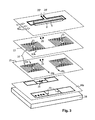
図面に示す、特に図2a〜2cに示すように、本発明による直交フラックスゲート式磁界センサー2は、飽和可能な強磁性被覆体8を備えた「励磁ロッド」被覆層であって、以下、そのように記述する、基本的に直線形の部位6をもつ励磁導電体4と、前記飽和可能な強磁性被覆体8の対向端14に近接配備されたコイル部12をもつセンサーピックアップコイル10とからなる。さらに、センサーには、前記被覆体8と励磁導電体4とが載置された基板16が備わる。
As shown in the drawings, in particular in FIGS. 2a-2c, an orthogonal fluxgate
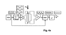
前記基板16は、セラミック材、ガラス材、または、その他の絶縁材料で作成可能である。しかしながら、基板16は、励磁導電体4に接続された、ピックアップコイル10を含む集積回路を備える半導体で作成するのが好ましい。そのような半導体で構成された回路の模範的な実施例を、図4aと4bのブロック図に示し、以下、それを説明する。
The
前記基板16が集積回路のない支持体として作用する例では、検出コイルおよび励磁導電体には、導電体を外部の信号処理励起回路に接続するため、それぞれ導体パッド18、20(図2a参照)が設けられる。基板16が集積回路で作成される場合には、図3の層16aとして図解的に示すように、導体の積層工程中に作成されるビア(スルーホール)21にて励磁導電体の端20を回路に直接に相互接続する。同様に、回路に対する異なる層間でのそれぞれのピックアップコイルの相互接続は、ビアつまり接続点23にて行われる。
In the example where the
前記集積回路16aを備えた基板16は、CMOSなどの周知の半導体技術で作成可能であって、その場合、集積回路が形成された半導体層やピックアップコイルを形成する金属導電層が、基板上に直接に集積されて、部品16a、15、13からなる集積回路を構成し、その上に磁性材や励磁導電体が積層される。製造内容の一例を、下記に説明する。
The
前記検出コイル10は、平面形状であるのが好ましく、そうすれば、強磁性被覆体8の両端14に、コイル部12の中心がほぼ重なる。そのため、外部磁束線の強磁性被覆体側への屈曲により、両端14での集中度が最高値となり、基板の面と直交する外部磁界の最大の検出が可能となる。
The
ピックアップ感度を高めるには、図3に示すように、コイル部12を積み重ねられた2つの層13、15に設けられた2組の螺旋形状12a、12bで形成して、検出コイルの巻線数を2倍にするのが望ましい。実際上、コイル中心の外側の接続点18への経路を確保するには、検出コイルには2つの層が一般的に必要であるため、前記追加コイルは別の層を追加する必要はなく、製造工程が複雑になることもない。ただし、測定感度をより高めるようとすれば、別の層を追加することも可能である。
In order to increase the pickup sensitivity, as shown in FIG. 3, the
前記被覆体8は、「パーマロイ」などの周知の強磁性材で形成するのが好ましいが、たやすく飽和し、ヒステレシスが低い軟磁性材を使用しても構わない。強磁性材の長所は、本発明によるセンサーを製造するための最新製造技術において、積層が簡単に行えることである。励磁導電体部やピックアップコイルの材料としては、銅や銅合金が望ましいが、導電性が高い非磁性材の使用も可能である。
The
図4aを参照して、直接モードで作動する信号処理回路の第1動作例を、簡単に説明する。最初に、周波数foのクロック信号Clkが、信号発生器GENで作成される。その信号の周波数は、1/2に分割され、ドライバにより、奇数高調波とゼロオフセットをもつ正弦波、三角波、パルス波などの電圧波形に変換される。その電圧波形は、さらに電流波形に変換され、強磁性コア部の励起ロッドへ送られる。電流波形のレベルは、強磁性コア部を飽和できるほど充分に高い値でなければならない。その周期飽和作用により、コア部の端の下方に位置するピックアップコイルの端部に、外部磁界Hextに比例した誘電電圧が発生する。誘電電圧は、増幅され、復調器DEMで同期整流される。その整流信号は、カットオフ周波数がfo値より低いローパスフィルタに送られる。ローパスフィルタの出力は、センサー測定範囲内の外部磁界Hextに比例するDC電圧となる。 A first operation example of the signal processing circuit operating in the direct mode will be briefly described with reference to FIG. 4a. First, a clock signal Clk having a frequency f o is generated by the signal generator GEN. The frequency of the signal is divided into ½, and is converted into a voltage waveform such as a sine wave, a triangular wave, or a pulse wave having odd harmonics and zero offset by a driver. The voltage waveform is further converted into a current waveform and sent to the excitation rod of the ferromagnetic core portion. The level of the current waveform must be high enough to saturate the ferromagnetic core. Due to the periodic saturation action, a dielectric voltage proportional to the external magnetic field H ext is generated at the end of the pickup coil located below the end of the core. The dielectric voltage is amplified and synchronously rectified by a demodulator DEM. The rectified signal is sent to a low-pass filter whose cut-off frequency is lower than the f o value. The output of the low-pass filter is a DC voltage proportional to the external magnetic field H ext within the sensor measurement range.
図4bを参照して、フィードバックモードで作動する信号処理回路の第2動作例を、簡単に説明する。まず、周波数foのクロック信号Clkが、信号発生器GENで作成される。その信号の周波数は、1/2に分割され、ドライバにより、奇数高調波とゼロオフセットをもつ正弦波、三角波、パルス波などの電圧波形に変換される。その電圧波形は、さらに電流波形に変換され、強磁性コア部の励起ロッドへ送られる。電流波形のレベルは、強磁性コア部を飽和できるほど充分に高い値でなければならない。その周期飽和作用により、コア部の端の下方に位置するピックアップコイルの端部に、外部磁界Hextに比例した誘電電圧が発生する。誘電電圧は、増幅され、復調器DEMで同期整流される。その整流信号は、積分器で積分処理され、電圧/電流変換器へ送られる。その変換電流は、外部磁界Hextとは反対方向の補償磁界Hcompを作成するフィードバックコイルへ送られ、そのため、ピックアップコイルの端部における誘電電圧が低下する。システムが安定状態のときは、フィードバックコイルへの電流は外部磁界の電流レベルと同じレベル値であるため、コア部周囲の磁界全体がゼロとなって、ピックアップコイルに誘電電圧が発生することはない。そのため、増幅器と復調器の出力値もゼロとなり、積分器の出力は、外部磁界Hextに比例するDC電圧となる。 A second operation example of the signal processing circuit operating in the feedback mode will be briefly described with reference to FIG. 4b. First, a clock signal Clk having a frequency f o is generated by the signal generator GEN. The frequency of the signal is divided into ½, and is converted into a voltage waveform such as a sine wave, a triangular wave, or a pulse wave having odd harmonics and zero offset by a driver. The voltage waveform is further converted into a current waveform and sent to the excitation rod of the ferromagnetic core portion. The level of the current waveform must be high enough to saturate the ferromagnetic core. Due to the periodic saturation action, a dielectric voltage proportional to the external magnetic field H ext is generated at the end of the pickup coil located below the end of the core. The dielectric voltage is amplified and synchronously rectified by a demodulator DEM. The rectified signal is integrated by an integrator and sent to a voltage / current converter. The converted current is sent to a feedback coil that creates a compensation magnetic field H comp in a direction opposite to the external magnetic field H ext , thereby reducing the dielectric voltage at the end of the pickup coil. When the system is in a stable state, the current to the feedback coil has the same level as the current level of the external magnetic field, so the entire magnetic field around the core is zero, and no dielectric voltage is generated in the pickup coil. . Therefore, the output values of the amplifier and the demodulator are also zero, and the output of the integrator is a DC voltage proportional to the external magnetic field H ext .
図5に示すのは、本発明によるセンサー製造法の処理内容の一例としての、積層工程の順序である。図5の左側の部分は、センサー積層の縦断面図であって、右側の部分は、横断面図である。 FIG. 5 shows the order of the laminating process as an example of the processing content of the sensor manufacturing method according to the present invention. The left part of FIG. 5 is a longitudinal sectional view of the sensor stack, and the right part is a transverse sectional view.
第1の工程(a)では、励起ロッドのための下側層のピックアップコイル12aと接触パッド20が、スパッタリングなどの周知の金属積層技術により基板上に形成され、続いて、フォトリソグラフ法とエッチング法によりパターン化処理が行われて、例えば、AlSi1%のアルミ合金の金属層が形成される。
In the first step (a), the
次の工程(b)では、例えば、スパッタリングによりSiO2の接触層が積層され、続いて、フォトリソグラフ法とエッチング法によりパターン化処理が行われるが、特に、2層のピックアップコイル12a、12bを相互接続するためのビア21、23が形成され、さらに工程(c)では、工程(a)と同じ方法で第2のコイル層12bが積層される。
In the next step (b), for example, a contact layer of SiO 2 is laminated by sputtering, followed by patterning by a photolithographic method and an etching method. In particular, two layers of
工程(d)では、例えば、スピン法によりSU−8の絶縁層が積層され、続いて、フォトリソグラフ法が実施され、工程(e)では、例えば、蒸着法によりCr/Cuの電気メッキのためのシード層が前記層上に積層される。 In the step (d), for example, an SU-8 insulating layer is stacked by a spin method, and subsequently, a photolithographic method is performed. In the step (e), for example, for electroplating of Cr / Cu by a vapor deposition method. A seed layer is laminated on the layer.
工程(f)では、例えば、スピン法によりAZ9260のモールド層(非特許文献4)が前記層上に積層され、続いて、フォトリソグラフ法が行われて、強磁性被覆体の基礎部8aを形成するのに必要な開孔を露出させ、例えば、電気メッキ法によりパーマロイ(Fe19Ni81)の強磁性被覆体が積層された後、工程(g)に示すようにモールド層を除去する。
In the step (f), for example, a AZ9260 mold layer (Non-patent Document 4) is laminated on the layer by a spin method, and then a photolithographic method is performed to form the
さらに、工程(h)では、スピン法により別のモールド層が積層され、続いて、フォトリソグラフ法の後、銅の電気メッキにより導電性励起ロッド6が形成されて、その後で、工程(i)に示すようにモールド層を除去する。励起ロッドは、駆動回路への接続のための
ビア21に接続される。
Further, in the step (h), another mold layer is laminated by the spin method, and subsequently, the
次の工程(j)では、スピン法によりモールド層が積層され、続いて、部分的に形成された強磁性基礎層8aと励起ロッド6の周囲でフォトリソグラフ法が行われて、工程(k)に示すように、励起ロッド周囲の強磁性被覆体8の残り部分の電気メッキを実施した後、最後の工程(l)で、シード層の露出した残り部分をエッチング法で除去する。
In the next step (j), a mold layer is laminated by a spin method, and subsequently, a photolithographic method is performed around the partially formed
CMOS技術を採用した場合には、ピックアップコイルは集積回路に集積形成されているため、言い換えれば、工程(a)から工程(d)までの同様の工程がCMOS技術工程に含まれているため、工程(e)以降のシード層の形成から追加処理を開始すればよい。 When the CMOS technology is adopted, the pickup coil is integrated in the integrated circuit. In other words, the CMOS technology step includes the same steps from the step (a) to the step (d). What is necessary is just to start an additional process from formation of the seed layer after a process (e).
Claims (8)
Applications Claiming Priority (2)
| Application Number | Priority Date | Filing Date | Title |
|---|---|---|---|
| EP05405451A EP1746430A1 (en) | 2005-07-22 | 2005-07-22 | Orthogonal fluxgate magnetic field sensor |
| PCT/IB2006/002007 WO2007010378A1 (en) | 2005-07-22 | 2006-07-17 | Orthogonal fluxgate magnetic field sensor |
Publications (1)
| Publication Number | Publication Date |
|---|---|
| JP2009503443A true JP2009503443A (en) | 2009-01-29 |
Family
ID=36001158
Family Applications (1)
| Application Number | Title | Priority Date | Filing Date |
|---|---|---|---|
| JP2008522085A Withdrawn JP2009503443A (en) | 2005-07-22 | 2006-07-17 | Orthogonal fluxgate magnetic field sensor |
Country Status (5)
| Country | Link |
|---|---|
| US (1) | US7834620B2 (en) |
| EP (2) | EP1746430A1 (en) |
| JP (1) | JP2009503443A (en) |
| CN (1) | CN101228453A (en) |
| WO (1) | WO2007010378A1 (en) |
Cited By (1)
| Publication number | Priority date | Publication date | Assignee | Title |
|---|---|---|---|---|
| WO2019017066A1 (en) * | 2017-07-21 | 2019-01-24 | 朝日インテック株式会社 | Ultra-small high-sensitivity magnetic sensor |
Families Citing this family (36)
| Publication number | Priority date | Publication date | Assignee | Title |
|---|---|---|---|---|
| EP2037286A1 (en) * | 2007-09-13 | 2009-03-18 | Micronas GmbH | Measuring device for measuring a magnetic field |
| EP2071346A1 (en) * | 2007-12-14 | 2009-06-17 | Liaisons Electroniques-Mecaniques Lem S.A. | Thin film fluxgate sensor |
| DE102009028956A1 (en) * | 2009-08-28 | 2011-03-03 | Robert Bosch Gmbh | magnetic field sensor |
| DE102009044988A1 (en) * | 2009-09-24 | 2011-03-31 | Robert Bosch Gmbh | Optimized control of a fluxgate sensor |
| US8508218B2 (en) * | 2011-05-11 | 2013-08-13 | Sensima Technology Sa | Hall-effect-based angular orientation sensor and corresponding method |
| JP5866706B2 (en) * | 2011-09-09 | 2016-02-17 | 国立大学法人九州大学 | Magnetic field sensor |
| US9354257B2 (en) * | 2011-11-04 | 2016-05-31 | General Electric Company | Systems and methods for use in measuring current through a conductor |
| JP5364816B1 (en) | 2012-06-08 | 2013-12-11 | 株式会社フジクラ | Magnetic element control device, magnetic element control method, and magnetic detection device |
| JP5393844B2 (en) * | 2012-06-08 | 2014-01-22 | 株式会社フジクラ | Magnetic element control device, magnetic element control method, and magnetic detection device |
| US9176203B2 (en) | 2013-02-05 | 2015-11-03 | Texas Instruments Incorporated | Apparatus and method for in situ current measurement in a conductor |
| WO2014152650A1 (en) | 2013-03-14 | 2014-09-25 | California Institute Of Technology | Detecting electrical and electrochemical energy units abnormalities |
| CN103323794B (en) * | 2013-06-21 | 2015-07-15 | 中国人民解放军国防科学技术大学 | GMR-MEMS integrated weak magnetic sensor adopting plane micro-coil |
| RU2533345C1 (en) * | 2013-06-28 | 2014-11-20 | Федеральное государственное унитарное предприятие "Всероссийский научно-исследовательский институт автоматики им. Н.Л. Духова" (ФГУП "ВНИИА") | Measurement method of amplitude of bidirectional pulse of magnetic field |
| US9825347B2 (en) * | 2013-10-07 | 2017-11-21 | Koninklijke Philips N.V. | Precision batch production method for manufacturing ferrite rods |
| JP6288684B2 (en) | 2013-10-17 | 2018-03-07 | 公立大学法人大阪市立大学 | Current measuring device and current measuring method |
| KR101532150B1 (en) * | 2013-12-09 | 2015-06-26 | 삼성전기주식회사 | Othogonal type fluxgate sensor |
| WO2016100919A1 (en) | 2014-12-19 | 2016-06-23 | California Institute Of Technology | Improved systems and methods for management and monitoring of energy storage and distribution |
| US10878997B2 (en) | 2015-03-13 | 2020-12-29 | Taiwan Semiconductor Manufacturing Company, Ltd. | Integrated circuit having current-sensing coil |
| CN104808157B (en) * | 2015-04-11 | 2017-10-24 | 西北工业大学 | A kind of printed circuit board orthogonal fluxgate sensor |
| US11092656B2 (en) * | 2015-05-12 | 2021-08-17 | Texas Instruments Incorporated | Fluxgate magnetic field detection method and circuit |
| US10330732B2 (en) | 2015-10-01 | 2019-06-25 | California Institute Of Technology | Systems and methods for monitoring characteristics of energy units |
| CN105676151B (en) * | 2016-01-18 | 2018-06-22 | 华东师范大学 | A kind of negative feedback magnetic field sensor |
| US10184991B2 (en) * | 2016-05-11 | 2019-01-22 | Texas Instruments Incorporated | Dual-axis fluxgate device |
| US11008650B2 (en) | 2016-11-03 | 2021-05-18 | Starfire Industries Llc | Compact system for coupling RF power directly into RF linacs |
| US20200273684A1 (en) * | 2019-02-25 | 2020-08-27 | Starfire Industries Llc | Method and apparatus for metal and ceramic nanolayering for accident tolerant nuclear fuel, particle accelerators, and aerospace leading edges |
| FR3060757B1 (en) * | 2016-12-19 | 2020-11-06 | Safran Electronics & Defense | FLOW VALVE CURRENT SENSOR |
| EP3382409B1 (en) * | 2017-03-31 | 2022-04-27 | AT & S Austria Technologie & Systemtechnik Aktiengesellschaft | Component carrier with integrated flux gate sensor |
| JP7262885B2 (en) * | 2017-06-16 | 2023-04-24 | 朝日インテック株式会社 | Ultra-sensitive micro magnetic sensor |
| EP3514559B1 (en) * | 2018-01-22 | 2021-08-25 | Melexis Technologies SA | Sensor package |
| EP3514502B1 (en) | 2018-01-22 | 2021-07-14 | Melexis Technologies SA | Inductive position sensor |
| FR3083321B1 (en) * | 2018-06-27 | 2021-03-05 | Safran Electronics & Defense | FLOW VALVE CURRENT SENSOR |
| CN109358301A (en) * | 2018-09-29 | 2019-02-19 | 河南理工大学 | A kind of micro fluxgate sensor based on sewing formula core structure |
| CN109507474A (en) * | 2018-12-04 | 2019-03-22 | 上海波卉电源科技有限公司 | Superhigh precision high-low pressure current sampling technique is realized with numerical control fluxgate |
| AT522600B1 (en) * | 2019-04-15 | 2023-03-15 | Braunschmid Dipl Ing Msc Franz | Flat coil for wireless power transmission |
| EP3812785A1 (en) * | 2019-10-22 | 2021-04-28 | LEM International SA | Fluxgate current transducer |
| CN111123177B (en) * | 2020-01-20 | 2022-06-17 | 河南理工大学 | Folding multilayer iron core orthogonal fluxgate sensor |
Family Cites Families (6)
| Publication number | Priority date | Publication date | Assignee | Title |
|---|---|---|---|---|
| US3218547A (en) * | 1961-11-29 | 1965-11-16 | Ling Sung Ching | Flux sensing device using a tubular core with toroidal gating coil and solenoidal output coil wound thereon |
| JPS5024183B1 (en) * | 1970-12-03 | 1975-08-13 | ||
| JP4007464B2 (en) * | 1997-10-06 | 2007-11-14 | Tdk株式会社 | Magnetic detector |
| FR2802649B1 (en) * | 1999-12-17 | 2002-02-08 | Commissariat Energie Atomique | FLOW GATE MICROMAGNETOMETER WITH PERPENDICULAR DETECTION AND METHOD FOR PRODUCING THE SAME |
| EP1260825A1 (en) * | 2001-05-25 | 2002-11-27 | Sentron Ag | Magnetic field probe |
| JP4695325B2 (en) * | 2001-09-17 | 2011-06-08 | キヤノン電子株式会社 | Magnetic detection element, method of manufacturing the same, and portable device using the element |
-
2005
- 2005-07-22 EP EP05405451A patent/EP1746430A1/en not_active Withdrawn
-
2006
- 2006-07-17 US US11/989,184 patent/US7834620B2/en active Active
- 2006-07-17 EP EP06779889A patent/EP1907872A1/en not_active Withdrawn
- 2006-07-17 CN CNA2006800268697A patent/CN101228453A/en active Pending
- 2006-07-17 WO PCT/IB2006/002007 patent/WO2007010378A1/en not_active Application Discontinuation
- 2006-07-17 JP JP2008522085A patent/JP2009503443A/en not_active Withdrawn
Cited By (4)
| Publication number | Priority date | Publication date | Assignee | Title |
|---|---|---|---|---|
| WO2019017066A1 (en) * | 2017-07-21 | 2019-01-24 | 朝日インテック株式会社 | Ultra-small high-sensitivity magnetic sensor |
| JP2019020346A (en) * | 2017-07-21 | 2019-02-07 | 朝日インテック株式会社 | Ultra-micro sensitive magnetic sensor |
| US11262419B2 (en) | 2017-07-21 | 2022-03-01 | Asahi Intecc Co., Ltd. | Ultra-small and high-sensitivity magnetic sensor |
| JP7262886B2 (en) | 2017-07-21 | 2023-04-24 | 朝日インテック株式会社 | Ultra-compact high-sensitivity magnetic sensor |
Also Published As
| Publication number | Publication date |
|---|---|
| US7834620B2 (en) | 2010-11-16 |
| EP1907872A1 (en) | 2008-04-09 |
| CN101228453A (en) | 2008-07-23 |
| WO2007010378A1 (en) | 2007-01-25 |
| EP1746430A1 (en) | 2007-01-24 |
| US20090230955A1 (en) | 2009-09-17 |
Similar Documents
| Publication | Publication Date | Title |
|---|---|---|
| JP2009503443A (en) | Orthogonal fluxgate magnetic field sensor | |
| Liakopoulos et al. | A micro-fluxgate magnetic sensor using micromachined planar solenoid coils | |
| KR101965977B1 (en) | Apparatus for measuring current | |
| JP4368797B2 (en) | Magnetic field sensor and method of operating magnetic field sensor | |
| JP5250108B2 (en) | Magnetic balanced current sensor | |
| KR100468833B1 (en) | A device for detecting magnetic field and a module for detecting magnetic field using the same | |
| KR101267246B1 (en) | Flux gate senior and electronic azimuth indicator making use thereof | |
| EP1387179B1 (en) | Printed circuit board integrated with a two-axis fluxgate sensor and method for manufacturing the same | |
| WO2012043738A1 (en) | Semiconductor integrated circuit, magnetism detection device, electronic compass, and ammeter | |
| KR100464093B1 (en) | Fluxgate sensor integrated in print circuit board and method for manufacturing the same | |
| CN103069282B (en) | Magnetic-balance current sensor | |
| JP2009535616A (en) | Thin film type triaxial fluxgate and manufacturing method thereof | |
| JP2004226410A (en) | Field sensing element integrated on semiconductor substrate and method for producing it | |
| WO2011155527A1 (en) | Flux gate sensor, electronic direction finder using same, and current meter | |
| US20030006763A1 (en) | Magnetic impedance element | |
| US6998840B2 (en) | Fluxgate sensor integrated having stacked magnetic cores in printed circuit board and method for manufacturing the same | |
| Perez et al. | Planar fluxgate sensor with an electrodeposited amorphous core | |
| WO2010020648A1 (en) | A fluxgate sensor | |
| JP2003270308A (en) | Magnetic field detecting element integrated on semiconductor substrate and manufacturing method therefor | |
| Delevoye et al. | Microfluxgate sensors for high frequency and low power applications | |
| Choi et al. | The microfluxgate magnetic sensor having closed magnetic path | |
| JP2004538467A (en) | Magnetic field detection device | |
| JP2004538467A6 (en) | Magnetic field detector | |
| Liakopoulos et al. | A micro fluxgate magnetic sensor using micromachined 3-dimensional planar coils | |
| JPH08201061A (en) | Thin film magnetic sensor |
Legal Events
| Date | Code | Title | Description |
|---|---|---|---|
| A621 | Written request for application examination |
Free format text: JAPANESE INTERMEDIATE CODE: A621 Effective date: 20090402 |
|
| A761 | Written withdrawal of application |
Free format text: JAPANESE INTERMEDIATE CODE: A761 Effective date: 20100723 |