EP2071346A1 - Thin film fluxgate sensor - Google Patents
Thin film fluxgate sensor Download PDFInfo
- Publication number
- EP2071346A1 EP2071346A1 EP07024346A EP07024346A EP2071346A1 EP 2071346 A1 EP2071346 A1 EP 2071346A1 EP 07024346 A EP07024346 A EP 07024346A EP 07024346 A EP07024346 A EP 07024346A EP 2071346 A1 EP2071346 A1 EP 2071346A1
- Authority
- EP
- European Patent Office
- Prior art keywords
- layer
- sections
- feed
- magnetic material
- excitation current
- Prior art date
- Legal status (The legal status is an assumption and is not a legal conclusion. Google has not performed a legal analysis and makes no representation as to the accuracy of the status listed.)
- Withdrawn
Links
Images

Classifications
-
- G—PHYSICS
- G01—MEASURING; TESTING
- G01R—MEASURING ELECTRIC VARIABLES; MEASURING MAGNETIC VARIABLES
- G01R33/00—Arrangements or instruments for measuring magnetic variables
- G01R33/02—Measuring direction or magnitude of magnetic fields or magnetic flux
- G01R33/04—Measuring direction or magnitude of magnetic fields or magnetic flux using the flux-gate principle
-
- G—PHYSICS
- G01—MEASURING; TESTING
- G01R—MEASURING ELECTRIC VARIABLES; MEASURING MAGNETIC VARIABLES
- G01R15/00—Details of measuring arrangements of the types provided for in groups G01R17/00 - G01R29/00, G01R33/00 - G01R33/26 or G01R35/00
- G01R15/14—Adaptations providing voltage or current isolation, e.g. for high-voltage or high-current networks
- G01R15/18—Adaptations providing voltage or current isolation, e.g. for high-voltage or high-current networks using inductive devices, e.g. transformers
- G01R15/183—Adaptations providing voltage or current isolation, e.g. for high-voltage or high-current networks using inductive devices, e.g. transformers using transformers with a magnetic core
- G01R15/185—Adaptations providing voltage or current isolation, e.g. for high-voltage or high-current networks using inductive devices, e.g. transformers using transformers with a magnetic core with compensation or feedback windings or interacting coils, e.g. 0-flux sensors
Definitions
- the present invention relates to a thin film fluxgate sensor for measuring or detecting magnetic fields.
- the measurement or detection of magnetic fields may be used in many different applications, for example for the measurement of electrical currents, for position sensing applications, or for measuring magnetic flux in electro-magnetic drive applications.
- Thin film fluxgate magnetic field sensors are used in applications that require low cost, miniature sensors for measuring weak magnetic fields.
- a thin film fluxgate sensor is described in international publication WO 2007/010378 .
- the fluxgate sensor described in the afore-mentioned application is manufactured by building up layers on a substrate using per se well-known deposition techniques.
- the fluxgate sensor has a central excitation conductor surrounded by a cladding of saturable soft magnetic material.
- the deposition process requires deposing a first layer of cladding, then deposing a layer of conducting material to form the central excitation conductor, and subsequently deposing thereon a second layer of cladding to completely wrap around the conductor.
- the soft magnetic material cladding is thus deposed in two or more deposition steps, with the disadvantage that this may create interfaces between the multiple layers that influence the magnetic flux lines passing through the cladding.
- the interface may create a parasitic air gap effect that increase the level of magnetisation required for saturation of the cladding (and thus the power required to drive the sensor) and/or reduce the uniformity of magnetisation thus leading to uneven saturation of the cladding and distortion of the sensor measurement signal.
- An object of this invention is to provide a thin film fluxgate magnetic field sensor that is accurate, power efficient, compact, and economical to manufacture in industrial series.
- a fluxgate magnetic field sensor including an electrical excitation current conductor and a layer of saturable magnetic material cladding having a plurality of feed-through channels extending between opposed faces of the layer, the excitation current conductor weaving through a plurality of said feed-through channels.
- the saturable magnetic material cladding can be deposed in a single continuous layer thus avoiding interfaces that create parasitic air gap effect and resistance to magnetic flux. Moreover, the effective lengths of sections of cladding around each feed-through channel, and therefore around portions of the excitation current conductor, are short, resulting in a good uniformity of saturation of the saturable magnetic material.
- the channels are preferably arranged in a juxtaposed manner at a substantially regular spacing in a line, or alternatively in a zigzag pattern.
- a plurality of lines of cladding in which feed-through channels are formed may be provided, one line next to the other in contact eith each other or spaced apart.
- a single excitation current conductor may be provided, weaving through the plurality of lines, from one end of the line to the other end and back.
- a plurality of separate excitation current conductors, each weaving through different lines of cladding may be provided.
- the different lines of magnetic material cladding may have equal or different lengths.
- the saturation characteristics of the saturable magnetic material cladding may thus be varied or tuned by varying the respective lengths of adjacent cladding lines.
- the sensitivity of the fluxgate sensor may be easily varied by varying the length of the cladding.
- the fluxgate sensor may advantageously include a sensor coil that spirals around the one or more lines of magnetic material cladding and excitation current conductor, the sensor coil spiral comprising planar sections formed either side of the magnetic material cladding layer, the planar sections being interconnected by feed-through sections spanning across the magnetic material cladding layer.
- the planar sections of sensor coil may advantageously be formed in the same layers as the planar sections of excitation current conductor interconnecting adjacent feed-through channels. The deposition process to form the fluxgate sensor is thus very economical, in view of the limited number of layers to be patterned and deposited.
- a method of making the fluxgate magnetic field sensor according to this invention may include the steps of depositing a first conductive layer comprising sections of the excitation current conductor, depositing a layer of soft magnetic material forming the cladding with a plurality of feed-through channels between opposite outer faces of the soft magnetic material layer, depositing conductive portions representing sections of the conductor carrying the saturation current.
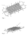
- a fluxgate magnetic field sensor 2 comprises an excitation current carrying conductor 4, a saturable magnetic material cladding 6, a magnetic field sensor 8 and a substrate 10 carrying the afore-mentioned elements.
- Extremities of the excitation current conductor 4 are connected to contact terminals 13a, 13b, in the embodiments shown in form of contact pads for connection to an excitation current supply (not shown) of the sensor.
- the magnetic field sensor 8 is in the form a sensing coil that spires around the magnetic material cladding, extremities of the sensing coil being connected to contact terminals 12a, 12b which in the embodiments shown are in the form of contact pads for connection to a sensing coil processing circuit (not shown) of the sensor.
- the magnetic field sensor may however have other configurations, for example the magnetic field sensor could comprise one or more pick-up coils, for example in a planar arrangement on the substrate and positioned at extremities of the magnetic material cladding 6.
- the magnetic material cladding 6 may be arranged in one or a plurality of lines 14 in a layer that can be formed by a process of deposition and patterning of a layer of magnetic material.
- the layer of magnetic material cladding arranged in one or more lines may also be formed by methods other than deposition, for example by injection moulding around the excitation current conductor.
- the deposition process for forming the sensor according to this invention is however particularly advantageous, in that it is very cost effective for high volume industrial manufacturing and enables the sensor to be particularly compact and power efficient.
- Each line of magnetic material cladding comprises a plurality of juxtaposed feed-through channels 16 that extend between opposed outer faces 18, 20 of the magnetic material cladding layer
- the feed-through channels 16 are preferably positioned at a regular spacing one from the other along a straight line as shown in the illustrated embodiments. It is however also possible to have the feed-through channels arranged along a zigzag pattern rather than along a single line.
- Each magnetic material cladding line preferably has an outer lateral contour 18 that substantially conforms to the shape of the feed-through channels such that the thickness of the cladding surrounding the feed-through channel is approximately constant.
- the magnetic material cladding thus resembles a juxtaposed plurality of integrally connected annular discs arranged along a straight line.
- the lateral outer contour 18 of each magnetic material cladding line could however follow a straight line or have a contour that does not conform to the shapes of the feed-through channels.
- the substantially regular thickness of the cladding from the feed-through channel to the outer contour however has the advantage of facilitating uniform saturation of the cladding due to the magnetic field generated by the excitation current flowing through the section 26 of excitation current conductor traversing the feed-through channels 16.
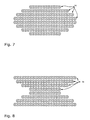
- the magnetic material cladding lines 14 can have identical lengths as shown in figure 1 , or have different lengths as shown in figures 7 and 8 .
- the cladding lines increase in length from the outer lines towards the inner lines, whereas in a variant of figure 8 the length of the cladding lines decreases from the outer lines towards the inner lines.
- Other configuration of line lengths could also be envisaged.
- the various line length configurations are selected to optimize the sensing of the external magnetic field to be measured by the sensing coil depending on the general orientation and intensity of the external magnetic field.
- the excitation current conductor 4 weaves through the feed-through channels 16, passing from one side 19 of the cladding layer to the opposite side 20 and back, and so on, from feed-through channel 16 to adjacent feed-through channel 16, as best seen in figures 1, 2 and 6 .
- the excitation current conductor thus has sections 22 in a first layer, sections 24 on a second layer, and feed-through sections 26 interconnecting the first and second layer sections 22, 24.
- the feed-through sections 26 pass through the feed-through channels 16 of the magnetic material cladding layer.
- the excitation current conductor has a bridging section 28 that interconnects the excitation current conductors of adjacent lines.
- each line or groups of lines of cladding with separate excitation conductors, each with there own contact pads for connection to an excitation current supply circuit, or connected in parallel at their respective ends to common contact pads for connection in parallel to an excitation current supply circuit.
- the magnetic field sensor is in the form of a sensing coil that spires around the line or plurality of lines of magnetic material cladding as illustrated in figure 1 .
- the spirals or windings of the sensing coil may advantageously comprise sections 30 in a first layer and sections 32 in a second layer, the first and second layers on opposite sides of the magnetic material cladding layer and interconnected by feed-through sections 34 that extend across the layer of cladding so as to form a continuous spiral.
- the first and second sections of the winding may advantageously be arranged in the same planes or layers as the respective sections 22, 24 of the excitation current conductor. The sections of sensing coil and excitation current conductor can thus be formed simultaneously during the deposition process.
- the deposition and patterning of the various layers can be performed by various known manufacturing techniques (including for example chemical vapour deposition, sputtering, plating, photolithographic etching and others).
Abstract
A fluxgate magnetic field sensor including an excitation current conductor (4) and a layer of saturable magnetic material cladding (6) having a plurality of feed-through channels (16) extending between opposed faces of the cladding layer, the excitation current conductor weaving through a plurality of said feed-through channels.
Description
- The present invention relates to a thin film fluxgate sensor for measuring or detecting magnetic fields.
- The measurement or detection of magnetic fields may be used in many different applications, for example for the measurement of electrical currents, for position sensing applications, or for measuring magnetic flux in electro-magnetic drive applications.
- Thin film fluxgate magnetic field sensors are used in applications that require low cost, miniature sensors for measuring weak magnetic fields. A thin film fluxgate sensor is described in international publication
WO 2007/010378 . The fluxgate sensor described in the afore-mentioned application is manufactured by building up layers on a substrate using per se well-known deposition techniques. The fluxgate sensor has a central excitation conductor surrounded by a cladding of saturable soft magnetic material. The deposition process requires deposing a first layer of cladding, then deposing a layer of conducting material to form the central excitation conductor, and subsequently deposing thereon a second layer of cladding to completely wrap around the conductor. The soft magnetic material cladding is thus deposed in two or more deposition steps, with the disadvantage that this may create interfaces between the multiple layers that influence the magnetic flux lines passing through the cladding. In particular, the interface may create a parasitic air gap effect that increase the level of magnetisation required for saturation of the cladding (and thus the power required to drive the sensor) and/or reduce the uniformity of magnetisation thus leading to uneven saturation of the cladding and distortion of the sensor measurement signal. - In order to vary the sensitivity and measurement range of the fluxgate sensor, it may be desirable to vary the length of the fluxgate sensor. This is however difficult to achieve with conventional thin film fluxgate sensors while maintaining uniform saturation of the soft magnetic material and linearity of the signal measurement.
- An object of this invention is to provide a thin film fluxgate magnetic field sensor that is accurate, power efficient, compact, and economical to manufacture in industrial series.
- It is advantageous to provide a magnetic field sensor that has a high sensitivity.
- It is advantageous to provide a magnetic field sensor that generates a measurement signal with good linearity.
- It is advantageous to provide a fluxgate magnetic field sensor that can be easily configured for different operating ranges in an economical manner.
- Objects of this invention have been achieved by providing the fluxgate magnetic field sensor according to claim 1.
- Disclosed herein is a fluxgate magnetic field sensor including an electrical excitation current conductor and a layer of saturable magnetic material cladding having a plurality of feed-through channels extending between opposed faces of the layer, the excitation current conductor weaving through a plurality of said feed-through channels.
- Advantageously, the saturable magnetic material cladding can be deposed in a single continuous layer thus avoiding interfaces that create parasitic air gap effect and resistance to magnetic flux. Moreover, the effective lengths of sections of cladding around each feed-through channel, and therefore around portions of the excitation current conductor, are short, resulting in a good uniformity of saturation of the saturable magnetic material.
- The channels are preferably arranged in a juxtaposed manner at a substantially regular spacing in a line, or alternatively in a zigzag pattern. Advantageously, a plurality of lines of cladding in which feed-through channels are formed may be provided, one line next to the other in contact eith each other or spaced apart. A single excitation current conductor may be provided, weaving through the plurality of lines, from one end of the line to the other end and back. Alternatively, a plurality of separate excitation current conductors, each weaving through different lines of cladding, may be provided.
- The different lines of magnetic material cladding may have equal or different lengths. The saturation characteristics of the saturable magnetic material cladding may thus be varied or tuned by varying the respective lengths of adjacent cladding lines. In particular, the sensitivity of the fluxgate sensor may be easily varied by varying the length of the cladding.
- The fluxgate sensor may advantageously include a sensor coil that spirals around the one or more lines of magnetic material cladding and excitation current conductor, the sensor coil spiral comprising planar sections formed either side of the magnetic material cladding layer, the planar sections being interconnected by feed-through sections spanning across the magnetic material cladding layer. The planar sections of sensor coil may advantageously be formed in the same layers as the planar sections of excitation current conductor interconnecting adjacent feed-through channels. The deposition process to form the fluxgate sensor is thus very economical, in view of the limited number of layers to be patterned and deposited.
- A method of making the fluxgate magnetic field sensor according to this invention may include the steps of depositing a first conductive layer comprising sections of the excitation current conductor, depositing a layer of soft magnetic material forming the cladding with a plurality of feed-through channels between opposite outer faces of the soft magnetic material layer, depositing conductive portions representing sections of the conductor carrying the saturation current.
- In a preferred embodiment the manufacturing process may include the following steps:
- ■ deposit a conductive seed layer on an isolating substrate (e.g. glass, silicon)
- ■ pattern the seed layer to pattern the sections of the excitation current conductor and sections of the sensor coil on a first layer
- ■ electroplate a bottom conductive layer, for example with copper to form the sections of the excitation current conductor and sections of the sensor coil on the first layer
- ■ deposit an isolating layer, e.g. a polyimide, to insulate the excitation current and sensor conductors from the magnetic material layer
- ■ deposit a conductive seed layer
- ■ pattern this seed layer with the desired shape of the magnetic layer
- ■ electroplate permalloy or another soft magnetic material to form the magnetic material cladding layer
- ■ deposit an isolating layer, e.g. polyimide to insulate the excitation current and sensor conductors from the magnetic material layer
- ■ remove the isolating layer where conductive feed-throughs (vias) are desired
- ■ deposit and pattern a conductive seed layer to pattern the sections of the excitation current conductor and sections of the sensor coil on a second layer
- ■ electroplate the top conductive layer, for example with copper to form the sections of the excitation current conductor and sections of the sensor coil on the second layer
- Further objects and advantageous features of the invention will be apparent from the claims and following detailed description with reference to the figures in which:
-
Figures 1 and 2 are respective schematic views of a thin film fluxgate sensor according to this invention, illustrating the saturation conductor and lines of cladding; -
Figure 3 is a view showing a first conductive layer patterned to form sections of the excitation current conductor and sections of the sensing coil; -
Figure 4 is a view showing lines of magnetic material cladding and feed-through conductor sections of the excitation current conductor and the sensing coil; -
Figure 5 is a view of a second conductive layer patterned to form sections of the excitation current conductor and sections of the sensing coil; -
Figure 6 is a schematic cross-sectional view through a fluxgate sensor according to this invention showing the weaving of the excitation current conductor through the channels of the magnetic material cladding layer; -
Figure 7 is a view illustrating a plurality of lines of magnetic material cladding of different lengths according to a variant; -
Figure 8 is a view similar tofigure 7 of another variant; - Referring to the figures, a fluxgate
magnetic field sensor 2 comprises an excitation current carrying conductor 4, a saturablemagnetic material cladding 6, amagnetic field sensor 8 and a substrate 10 carrying the afore-mentioned elements. - Extremities of the excitation current conductor 4 are connected to
contact terminals - The
magnetic field sensor 8 is in the form a sensing coil that spires around the magnetic material cladding, extremities of the sensing coil being connected tocontact terminals - The magnetic field sensor may however have other configurations, for example the magnetic field sensor could comprise one or more pick-up coils, for example in a planar arrangement on the substrate and positioned at extremities of the magnetic material cladding 6.
- The
magnetic material cladding 6 may be arranged in one or a plurality oflines 14 in a layer that can be formed by a process of deposition and patterning of a layer of magnetic material. The layer of magnetic material cladding arranged in one or more lines, may also be formed by methods other than deposition, for example by injection moulding around the excitation current conductor. The deposition process for forming the sensor according to this invention is however particularly advantageous, in that it is very cost effective for high volume industrial manufacturing and enables the sensor to be particularly compact and power efficient. - Each line of magnetic material cladding comprises a plurality of juxtaposed feed-through
channels 16 that extend between opposedouter faces channels 16 are preferably positioned at a regular spacing one from the other along a straight line as shown in the illustrated embodiments. It is however also possible to have the feed-through channels arranged along a zigzag pattern rather than along a single line. - Each magnetic material cladding line preferably has an outer
lateral contour 18 that substantially conforms to the shape of the feed-through channels such that the thickness of the cladding surrounding the feed-through channel is approximately constant. The magnetic material cladding thus resembles a juxtaposed plurality of integrally connected annular discs arranged along a straight line. The lateralouter contour 18 of each magnetic material cladding line could however follow a straight line or have a contour that does not conform to the shapes of the feed-through channels. The substantially regular thickness of the cladding from the feed-through channel to the outer contour however has the advantage of facilitating uniform saturation of the cladding due to the magnetic field generated by the excitation current flowing through thesection 26 of excitation current conductor traversing the feed-throughchannels 16. - As best seen in
figure 1 , andfigures 7 and 8 , the magneticmaterial cladding lines 14 can have identical lengths as shown infigure 1 , or have different lengths as shown infigures 7 and 8 . In the variant offigure 7 , the cladding lines increase in length from the outer lines towards the inner lines, whereas in a variant offigure 8 the length of the cladding lines decreases from the outer lines towards the inner lines. Other configuration of line lengths could also be envisaged. The various line length configurations are selected to optimize the sensing of the external magnetic field to be measured by the sensing coil depending on the general orientation and intensity of the external magnetic field. - The excitation current conductor 4 weaves through the feed-through
channels 16, passing from oneside 19 of the cladding layer to theopposite side 20 and back, and so on, from feed-throughchannel 16 to adjacent feed-throughchannel 16, as best seen infigures 1, 2 and6 . The excitation current conductor thus hassections 22 in a first layer,sections 24 on a second layer, and feed-throughsections 26 interconnecting the first andsecond layer sections sections 26 pass through the feed-throughchannels 16 of the magnetic material cladding layer. Where there are a plurality of cladding lines with a single excitation current conductor 4 as illustrated infigures 1 and 2 , at the end of aline 14 the excitation current conductor has abridging section 28 that interconnects the excitation current conductors of adjacent lines. - It is however possible to provide each line or groups of lines of cladding with separate excitation conductors, each with there own contact pads for connection to an excitation current supply circuit, or connected in parallel at their respective ends to common contact pads for connection in parallel to an excitation current supply circuit.
- In a preferred embodiment, the magnetic field sensor is in the form of a sensing coil that spires around the line or plurality of lines of magnetic material cladding as illustrated in
figure 1 . The spirals or windings of the sensing coil may advantageously comprisesections 30 in a first layer andsections 32 in a second layer, the first and second layers on opposite sides of the magnetic material cladding layer and interconnected by feed-throughsections 34 that extend across the layer of cladding so as to form a continuous spiral. The first and second sections of the winding may advantageously be arranged in the same planes or layers as therespective sections - In a preferred embodiment the manufacturing process may include the following steps:
- ■ deposit a conductive seed layer on an isolating substrate (e.g. glass, silicon)
- ■ pattern the seed layer to pattern the
first layer sections 24 of the excitation current conductor andfirst layer sections 32 of the sensor coil - ■ electroplate or deposit by other means a bottom conductive layer, for example copper, to form the
sections 24 of the excitation current conductor andsections 32 of the sensor coil - ■ deposit an isolating layer, e.g. a polyimide, to insulate the excitation current and sensor conductors from the magnetic material layer
- ■ deposit a conductive seed layer
- ■ pattern this seed layer with the desired shape of the magnetic material layer
- ■ electroplate or deposit by other means permalloy or another soft magnetic material to form the magnetic
material cladding layer 6 - ■ deposit an isolating layer, e.g. polyimide to insulate the excitation current and sensor conductors from the magnetic material layer
- ■ remove the isolating layer where conductive feed-
throughs 26,34 (vias) are desired - ■ deposit and pattern a conductive seed layer to pattern the
second layer sections 22 of the excitation current conductor andsecond layer sections 30 of the sensor coil - ■ electroplate the second conductive seed layer, for example with copper, to form the
second layer sections 22 of the excitation current conductor andsecond layer sections 30 of the sensor coil - The deposition and patterning of the various layers can be performed by various known manufacturing techniques (including for example chemical vapour deposition, sputtering, plating, photolithographic etching and others).
Claims (12)
- A fluxgate magnetic field sensor including an excitation current conductor (4) and a layer of saturable magnetic material cladding (6) having a plurality of feed-through channels (16) extending between opposed faces of the cladding layer, the excitation current conductor weaving through a plurality of said feed-through channels.
- Magnetic field sensor according to claim 1 wherein the feed-through channels are arranged in a juxtaposed manner at a substantially regular spacing.
- Magnetic field sensor according to claim 1 or 2 wherein the feed-through channels are arranged in a straight line.
- Magnetic field sensor according to any one of the preceding claims wherein, the layer of magnetic material cladding comprises a plurality of separate lines (14) of cladding in which feed-through channels are formed.
- Magnetic field sensor according to claim 4, wherein lines of magnetic material cladding have different lengths.
- Magnetic field sensor according to any one of claims 3 to 5 wherein the excitation current conductor weaves through a plurality of lines.
- Magnetic field sensor according to any one of the preceding claims wherein, the excitation current conductor thus has sections (22) in a first layer, sections (24) on a second layer, and feed-through sections (26) passing through the feed-through channels (16) of the magnetic material cladding layer interconnecting the first and second layer sections (22, 24).
- Magnetic field sensor according to any one of the preceding claims further comprising a sensing coil that spirals around the layer of magnetic material cladding.
- Magnetic field sensor according to claim 8 wherein the sensing coil spiral comprises sections formed either side of the magnetic material cladding layer interconnected by feed-through sections spanning across the magnetic material cladding layer.
- Magnetic field sensor according to claim 9 wherein the sections of sensing coil are positioned in essentially the same respective planes either side of the magnetic cladding layer as sections of the excitation current conductor.
- A method of making a fluxgate magnetic field sensor including the steps of- depositing a first conductive layer comprising sections of the excitation current conductor,- depositing a layer of magnetic material forming the cladding with a plurality of feed-through channels between opposite outer faces of the soft magnetic material layer, and- depositing a second conductive layer of sections of the excitation current conductor.
- Method according to claim 11 wherein sections of a sensing coil are formed during the steps of depositing first and second conductive layers.
Priority Applications (6)
| Application Number | Priority Date | Filing Date | Title |
|---|---|---|---|
| EP07024346A EP2071346A1 (en) | 2007-12-14 | 2007-12-14 | Thin film fluxgate sensor |
| JP2010537592A JP5444245B2 (en) | 2007-12-14 | 2008-12-12 | Thin film fluxgate sensor |
| EP08862912A EP2232286B1 (en) | 2007-12-14 | 2008-12-12 | Thin-film fluxgate sensor |
| US12/747,784 US8339133B2 (en) | 2007-12-14 | 2008-12-12 | Thin film fluxgate sensor |
| PCT/IB2008/055270 WO2009077959A1 (en) | 2007-12-14 | 2008-12-12 | Thin film fluxgate sensor |
| CN200880120351.9A CN101896828B (en) | 2007-12-14 | 2008-12-12 | Thin film fluxgate sensor |
Applications Claiming Priority (1)
| Application Number | Priority Date | Filing Date | Title |
|---|---|---|---|
| EP07024346A EP2071346A1 (en) | 2007-12-14 | 2007-12-14 | Thin film fluxgate sensor |
Publications (1)
| Publication Number | Publication Date |
|---|---|
| EP2071346A1 true EP2071346A1 (en) | 2009-06-17 |
Family
ID=39402663
Family Applications (2)
| Application Number | Title | Priority Date | Filing Date |
|---|---|---|---|
| EP07024346A Withdrawn EP2071346A1 (en) | 2007-12-14 | 2007-12-14 | Thin film fluxgate sensor |
| EP08862912A Active EP2232286B1 (en) | 2007-12-14 | 2008-12-12 | Thin-film fluxgate sensor |
Family Applications After (1)
| Application Number | Title | Priority Date | Filing Date |
|---|---|---|---|
| EP08862912A Active EP2232286B1 (en) | 2007-12-14 | 2008-12-12 | Thin-film fluxgate sensor |
Country Status (5)
| Country | Link |
|---|---|
| US (1) | US8339133B2 (en) |
| EP (2) | EP2071346A1 (en) |
| JP (1) | JP5444245B2 (en) |
| CN (1) | CN101896828B (en) |
| WO (1) | WO2009077959A1 (en) |
Families Citing this family (9)
| Publication number | Priority date | Publication date | Assignee | Title |
|---|---|---|---|---|
| US10165276B2 (en) | 2010-09-30 | 2018-12-25 | Texas Instruments Incorporated | Method and apparatus for frame coding in vertical raster scan order for HEVC |
| US9176203B2 (en) | 2013-02-05 | 2015-11-03 | Texas Instruments Incorporated | Apparatus and method for in situ current measurement in a conductor |
| US9704637B2 (en) | 2013-07-15 | 2017-07-11 | Texas Instruments Incorporated | Method and apparatus for demagnetizing transformer cores in closed loop magnetic current sensors |
| US9291648B2 (en) | 2013-08-07 | 2016-03-22 | Texas Instruments Incorporated | Hybrid closed-loop/open-loop magnetic current sensor |
| US9261571B2 (en) | 2013-08-15 | 2016-02-16 | Texas Instruments Incorporated | Fluxgate magnetic sensor readout apparatus |
| US9229066B2 (en) | 2013-08-15 | 2016-01-05 | Texas Instruments Incorporated | Integrated fluxgate magnetic sensor and excitation circuitry |
| US11448711B2 (en) | 2015-03-25 | 2022-09-20 | Texas Instruments Incorporated | Simulation models for integrated fluxgate magnetic sensors and other magnetic circuit components |
| US11092656B2 (en) | 2015-05-12 | 2021-08-17 | Texas Instruments Incorporated | Fluxgate magnetic field detection method and circuit |
| CN109358301A (en) * | 2018-09-29 | 2019-02-19 | 河南理工大学 | A kind of micro fluxgate sensor based on sewing formula core structure |
Citations (2)
| Publication number | Priority date | Publication date | Assignee | Title |
|---|---|---|---|---|
| WO2007010378A1 (en) | 2005-07-22 | 2007-01-25 | Liaisons Electroniques-Mecaniques Lem S.A. | Orthogonal fluxgate magnetic field sensor |
| EP1785738A2 (en) * | 2005-11-09 | 2007-05-16 | M.D. MICRO DETECTORS S.p.A. | Magnetic sensor, particularly for measuring the position and movement of an object, and related manufacturing method |
Family Cites Families (5)
| Publication number | Priority date | Publication date | Assignee | Title |
|---|---|---|---|---|
| JP3545074B2 (en) * | 1994-12-27 | 2004-07-21 | 独立行政法人 科学技術振興機構 | Magnetic detecting element and magnetic detecting module integrated on semiconductor substrate |
| KR100464093B1 (en) * | 2002-03-13 | 2005-01-03 | 삼성전기주식회사 | Fluxgate sensor integrated in print circuit board and method for manufacturing the same |
| KR100465335B1 (en) * | 2002-09-18 | 2005-01-13 | 삼성전자주식회사 | Sensing apparatus having pluxgate sensor |
| US6885074B2 (en) * | 2002-11-27 | 2005-04-26 | Freescale Semiconductor, Inc. | Cladded conductor for use in a magnetoelectronics device and method for fabricating the same |
| JP2004184232A (en) * | 2002-12-03 | 2004-07-02 | Matsushita Electric Ind Co Ltd | Magnetic sensing element, its manufacturing method and magnetic sensing device and azimuth sensor using the magnetic sensing element |
-
2007
- 2007-12-14 EP EP07024346A patent/EP2071346A1/en not_active Withdrawn
-
2008
- 2008-12-12 EP EP08862912A patent/EP2232286B1/en active Active
- 2008-12-12 WO PCT/IB2008/055270 patent/WO2009077959A1/en active Application Filing
- 2008-12-12 JP JP2010537592A patent/JP5444245B2/en active Active
- 2008-12-12 CN CN200880120351.9A patent/CN101896828B/en active Active
- 2008-12-12 US US12/747,784 patent/US8339133B2/en not_active Expired - Fee Related
Patent Citations (2)
| Publication number | Priority date | Publication date | Assignee | Title |
|---|---|---|---|---|
| WO2007010378A1 (en) | 2005-07-22 | 2007-01-25 | Liaisons Electroniques-Mecaniques Lem S.A. | Orthogonal fluxgate magnetic field sensor |
| EP1785738A2 (en) * | 2005-11-09 | 2007-05-16 | M.D. MICRO DETECTORS S.p.A. | Magnetic sensor, particularly for measuring the position and movement of an object, and related manufacturing method |
Also Published As
| Publication number | Publication date |
|---|---|
| EP2232286A1 (en) | 2010-09-29 |
| CN101896828B (en) | 2014-12-31 |
| US20100271017A1 (en) | 2010-10-28 |
| US8339133B2 (en) | 2012-12-25 |
| JP5444245B2 (en) | 2014-03-19 |
| WO2009077959A1 (en) | 2009-06-25 |
| EP2232286B1 (en) | 2013-02-13 |
| JP2011506958A (en) | 2011-03-03 |
| CN101896828A (en) | 2010-11-24 |
Similar Documents
| Publication | Publication Date | Title |
|---|---|---|
| US8339133B2 (en) | Thin film fluxgate sensor | |
| JP5110142B2 (en) | Magnetoimpedance sensor element and manufacturing method thereof | |
| EP2402778B1 (en) | Magnetoimpedance sensor element and method for manufacturing the same | |
| JP4674533B2 (en) | AC current detection coil | |
| US6683522B2 (en) | Planar miniature inductors and transformers | |
| CN101178417A (en) | High-precision rogowski current transformer | |
| US8680854B2 (en) | Semiconductor GMI magnetometer | |
| EP3255440A1 (en) | A current sensor and a method of manufacturing a current sensor | |
| JP2011506958A5 (en) | ||
| WO2002095775A1 (en) | Planar miniature inductors and transformers and miniature transformers for millimachined instruments | |
| US7423509B2 (en) | Coil comprising several coil branches and micro-inductor comprising one of the coils | |
| EP2960661B1 (en) | A modular current sensing system and a method of making a modular current sensing system | |
| CN109724630B (en) | Magnetic sensor with integrated solenoid | |
| JP2008203238A (en) | Current detecting device | |
| CN112204681B (en) | Method for producing a planar coil assembly and sensor head provided with such a planar coil assembly | |
| US6233834B1 (en) | Miniature transformers for millimachined instruments | |
| JP2009027102A (en) | Stacked coil, vibration sensor using stacked coil, and manufacturing method of the stacked coil | |
| EP1018653B1 (en) | Magnetic sensor having soft magnetic metallic element formed in zigzag shape | |
| CN112051431A (en) | Current sensor and measuring system comprising such a current sensor | |
| JP2004184232A (en) | Magnetic sensing element, its manufacturing method and magnetic sensing device and azimuth sensor using the magnetic sensing element | |
| JP5075489B2 (en) | Magnetic device and manufacturing method thereof | |
| JP5606021B2 (en) | Manufacturing method of current sensor | |
| WO1993012528A1 (en) | Thin film sensors | |
| JP2005085968A (en) | Wire-wound inductor and manufacturing method thereof | |
| US20040070479A1 (en) | Via-less electronic structures and methods |
Legal Events
| Date | Code | Title | Description |
|---|---|---|---|
| PUAI | Public reference made under article 153(3) epc to a published international application that has entered the european phase |
Free format text: ORIGINAL CODE: 0009012 |
|
| AK | Designated contracting states |
Kind code of ref document: A1 Designated state(s): AT BE BG CH CY CZ DE DK EE ES FI FR GB GR HU IE IS IT LI LT LU LV MC MT NL PL PT RO SE SI SK TR |
|
| AX | Request for extension of the european patent |
Extension state: AL BA HR MK RS |
|
| AKX | Designation fees paid | ||
| REG | Reference to a national code |
Ref country code: DE Ref legal event code: 8566 |
|
| STAA | Information on the status of an ep patent application or granted ep patent |
Free format text: STATUS: THE APPLICATION IS DEEMED TO BE WITHDRAWN |
|
| 18D | Application deemed to be withdrawn |
Effective date: 20091218 |