EP2037286A1 - Measuring device for measuring a magnetic field - Google Patents
Measuring device for measuring a magnetic field Download PDFInfo
- Publication number
- EP2037286A1 EP2037286A1 EP07017942A EP07017942A EP2037286A1 EP 2037286 A1 EP2037286 A1 EP 2037286A1 EP 07017942 A EP07017942 A EP 07017942A EP 07017942 A EP07017942 A EP 07017942A EP 2037286 A1 EP2037286 A1 EP 2037286A1
- Authority
- EP
- European Patent Office
- Prior art keywords
- measuring
- sensor
- measuring device
- plane
- measuring coil
- Prior art date
- Legal status (The legal status is an assumption and is not a legal conclusion. Google has not performed a legal analysis and makes no representation as to the accuracy of the status listed.)
- Withdrawn
Links
Images


Classifications
-
- G—PHYSICS
- G01—MEASURING; TESTING
- G01R—MEASURING ELECTRIC VARIABLES; MEASURING MAGNETIC VARIABLES
- G01R33/00—Arrangements or instruments for measuring magnetic variables
- G01R33/02—Measuring direction or magnitude of magnetic fields or magnetic flux
- G01R33/06—Measuring direction or magnitude of magnetic fields or magnetic flux using galvano-magnetic devices
- G01R33/07—Hall effect devices
Definitions
- the invention relates to a measuring device for measuring a magnetic field, comprising at least one measuring coil and at least one sensor for measuring low-frequency magnetic fields, which measuring coil and which sensor are positioned or positionable with their plane of extent respectively transversely to the flow direction of the magnetic field, wherein the measuring coil and the sensor is connected to a signal processing device with which an output signal substantially corresponding to the magnetic field can be generated as a function of a first measuring signal provided by the measuring coil and a second measuring signal provided by the Hall sensor.
- a sensor for measuring low-frequency magnetic fields is understood to mean a sensor which has a greater accuracy of measurement and / or measuring sensitivity than the measuring coil at low frequencies and / or at a constant magnetic field.
- the sensor for measuring the low-frequency magnetic fields may in particular be a Hall sensor and / or a magnetoresistive sensor.
- Such a measuring device which is provided for measuring a magnetic field generated by an electric current flowing in a conductor, is made of DE 698 02 203 T2 known.
- the measuring device has a printed circuit board with an opening which is penetrated by the electrical conductor normal to the plane of the circuit board.
- a Rogowski coil is applied, which circumscribes the current-carrying conductor.
- several Hall sensors are mounted on the circuit board, which are arranged at regular intervals around the conductor.
- the measuring device allows a broadband measurement of the electric current or the magnetic field induced by this, but is still relatively complicated and expensive. Also, the measuring device still has quite large dimensions
- the measuring coil, the sensor and the signal processing device are monolithically integrated in a semiconductor chip.
- the measuring coil can then be manufactured with methods of semiconductor production with precisely predetermined, reproducible dimensions.
- the measuring coil in the manufacture of the measuring device can be positioned very accurately relative to the sensor. The measuring device thereby enables a high measuring accuracy.
- the windings of the measuring coil essentially follow the outer contour of the semiconductor chip and / or a line approximately parallel to it. As a result, almost the entire magnetic flux passing through the chip area of the semiconductor chip can be used for the induction of an electrical voltage in the measuring coil.
- the measuring device thereby enables a high measuring sensitivity.
- the abovementioned object can also be achieved by the sensor and the signal processing device are monolithically integrated in a semiconductor chip arranged on the carrier.
- the carrier may be a rigid, electrically insulating plate or a flexible, electrically insulating film.
- the plane spanned by at least one turn of the measuring coil and the plane of extent of the sensor (of the sensors) are arranged substantially in the main extension plane of the semiconductor chip and / or parallel thereto.
- the sensor and / or the Measuring coil can then have a correspondingly large area, which allows a high sensitivity of the measuring device.
- the plane spanned by the at least one turn of the measuring coil and the plane of extent of the sensor (s) are arranged transversely and in particular approximately orthogonally on the main extension plane of the semiconductor chip.
- the sensor and, if necessary, the measuring coil then only require a relatively small chip area, so that the semiconductor chip can have compact dimensions and can be manufactured correspondingly inexpensively.
- the measuring coil has at least two spaced apart interconnect levels when the interconnects of a first interconnect level extend transversely and preferably at right angles to the interconnects of at least one second interconnect level, and if the interconnects of the first interconnect level are connected via vias to the interconnects of the at least one second interconnect level ,
- the measuring coil can then have a multiplicity of turns. If appropriate, it is even possible for the semiconductor chip, in addition to the interconnect plane having the interconnects for the measuring coil, to have at least one further interconnect plane in which interconnects required for the signal processing device and / or at least one further integrated circuit in the semiconductor chip are arranged.
- the measuring coil has a conductor track in at least one conductor track plane, which has a plurality of turns arranged one inside the other.
- the conductor can, for example, have a spiral or polygonal course.
- the measuring direction of the at least one measuring coil and the measuring direction of the at least one sensor are arranged transversely and in particular orthogonal to one another.
- Such an arrangement is preferably used for applications in which the magnetic field to be measured has a plurality of normally arranged components B x , B y , B z and in which these components are linked together.
- a Such measuring device can be used in particular in a motor vehicle.
- the sensor or its orthogonal projection is expediently arranged on the plane of extent of the measuring coil within the measuring coil.
- the chip area available on the semiconductor chip can then be utilized particularly well.
- the measuring device can be contained in a position, speed and / or acceleration sensor which has at least one magnetic pole having an encoder, which is mounted relative to the measuring device such that the magnetic poles are movable past the measuring device. With the help of the measuring device then the movement of the encoder over a wide speed range can be detected with great precision.
- the magnetic poles can have at least one permanent magnet and / or one pole coil.
- the encoder is mounted rotatably relative to the measuring device.
- Such an encoder can be used, for example, to detect the position, angular velocity and / or angular acceleration of a rotating machine part, such as a rotary machine.
- a shaft, a rotating part of an internal combustion engine or a rotor of an electric machine may be provided.
- the encoder is slidably mounted relative to the measuring device.
- a measuring device may in particular be arranged on a linear motor of a sliding guide and / or a valve stem.
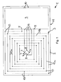
- An in Fig. 1 In the whole with 1 designated measuring device for measuring a magnetic field has a semiconductor chip 2, in which a measuring coil 3 and a Hall sensor 4 are monolithically integrated.
- the measuring coil 3 and the Hall sensor 4 are arranged with their extension planes each approximately in the plane defined by the semiconductor chip 2 plane, which the drawing plane in Fig. 1 equivalent.
- the magnetic flux of the magnetic field to be measured is transverse and preferably perpendicular to this plane.
- the measuring coil 3 has at its ends first electrical connections 5 to which a first measuring signal is applied, which corresponds to the induced voltage in a change in the magnetic field in the measuring coil 3 electrical voltage.
- the first first measurement signal is approximately proportional to the rate of change of the magnetic field, which is why higher-frequency signal components contained in the magnetic field are more strongly represented in the measurement signal are, as low-frequency signal components. Any DC component contained in the magnetic field does not cause a measurement signal at the measuring coil 3.
- the Hall sensor 4 has a Hall plate 6, are provided at the two spaced apart second electrical terminals 7, in which a constant current is fed, which is provided by a measuring current source not shown in detail in the drawing.
- Third electrical connections 8 for picking up a Hall voltage caused by the magnetic field are also provided on the Hall plate 6.
- the Hall voltage is hereinafter also referred to as the second measurement signal.
- both a DC component contained in the magnetic field and an AC component are taken into account. As the frequency of the magnetic field increases, however, the second measurement signal decreases.
- the first electrical connections 6 and the third electrical connections 8 are each connected to an input of a signal processing device 9, which is monolithically integrated into the semiconductor chip 2 as an electrical circuit.
- the signal processing device 9 generates in response to the first measurement signal and the second measurement signal an output signal corresponding to the magnetic field, which can be tapped off at an output 10.
- the output signal of the DC component of the magnetic field and low-frequency and high-frequency components are equally taken into account, so that there is a nearly linear frequency response over a wide frequency range.
- the measuring coil 3 has several turns, which are each composed of a plurality of straight conductor pieces.
- the individual conductor track pieces each run along a line running parallel to the outer contour 11 of the semiconductor chip 2. Starting from the middle of the measuring coil 3 to the edge of the semiconductor chip 2, the length of the straight conductor track pieces increases from turn to turn.
- the measuring coil 3 has two conductor track planes spaced parallel to one another.
- the interconnects 12a of a first interconnect level are shown in the drawing as a solid line and the interconnects 12b of a second interconnect level as dashed lines. It can clearly be seen that the interconnects 12a of the first interconnect level in the plan view of the semiconductor chip 2 approximately at right angles extend to the interconnects 12b of the second interconnect level.
- the interconnects 12a, 12b of the different interconnect level are interconnected by plated-through holes.
- the Hall sensor 4 or its orthogonal projection on the plane of extension of the measuring coil 3 is arranged within the measuring coil 3 in the space bounded by the innermost turn.
- the interconnect tracks 14 between the Hall plate 6 and the signal processing device extend in the first interconnect level between the interconnects 12a.
- the plane in which the Hall plate 6 extends is arranged orthogonally to the main extension plane of the semiconductor chip 2.
- the turns of the measuring coil 3 run approximately parallel to the plane of the Hall plate. 6
- the measuring coil 3 has two conductor track planes spaced parallel to one another.
- the interconnects 12a of a first interconnect level are in the drawing as a solid line and the interconnects 12b of a second interconnect level and the vias 13 are each shown as dashed lines.
- the interconnects 12a of the first interconnect level extend approximately parallel to the interconnects 12b of the second interconnect level.
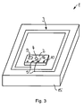
- the semiconductor chip 2 is arranged on a printed circuit board which has a planar carrier 15, on and / or in which an electrical conductor track is formed, which forms the measuring coil 3.
- the Hall sensor 4 and the signal processing device 9 are monolithically integrated into the semiconductor chip 2.
- the signal processing device 9 is electrically connected to the ends of the measuring coil 3 via connection contacts 16 provided on the semiconductor chip 2, for example via solder joints.
- the extension planes of the semiconductor chip 2 and the Hall plate of the Hall sensor 4 extend approximately parallel to the plane of the carrier 15.
- the turns of the measuring coil 3 extend substantially around the semiconductor chip 2 around.
- the printed circuit board 15 may comprise a plurality of layers with conductor tracks, which each form a portion of the measuring coil 3. This allows a larger number of turns.
- the individual interconnect layers can be connected in series via vias and / or connected to the terminal contacts 16.
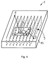
- the conductor tracks for the measuring coil 3 are arranged on the carrier 15 such that the planes spanned by the turns of the measuring coil 3 extend approximately orthogonally to the plane of extent of the carrier 15.
- the printed circuit board has two levels with tracks, which are spaced apart transversely to the plane of extension of the carrier 15.
- Each interconnect level has a plurality of conductor track pieces running approximately parallel to one another, which are connected via plated-through holes with interconnect pieces of a further interconnect level assigned to them.
- the semiconductor chip 2 is arranged above the measuring coil 3 on the carrier 15.
- the plane in which the semiconductor chip 2 extends extends approximately parallel to the plane of extent of the carrier 15.
- the Hall sensor 4 and the signal processing device 9 are monolithically integrated into the semiconductor chip 2.
- the signal processing device 9 is connected to the ends of the measuring coil 3 via connection contacts 16 provided on the semiconductor chip 2.
- the plane in which the Hall plate 6 extends is arranged orthogonal to the extension plane of the semiconductor chip 2.
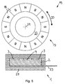
- the measuring device 1 can be arranged in a position, speed and / or acceleration sensor 19. This has a relative to the measuring device 1 in the direction of the double arrow 20 movably mounted encoder 17, which in the in Fig. 5 shown embodiment is configured as a rotatably mounted on an axis 21 encoder wheel.
- the encoder 17 has a plurality of approximately magnetized in the radial direction permanent magnetic magnetic poles 18 which are arranged on the outer circumference of the encoder 17 in the circumferential direction one behind the other. In each case, north and south poles alternate.
- the magnetic poles 18 are connected to each other on the inner circumference of the encoder by a magnetically conductive yoke 22.
- the magnetic poles 18 are movable past the measuring device 1 and thereby cause a magnetic alternating flux, which pass through the measuring coil 3 and the Hall plate 6 each approximately orthogonal to the plane of their extension.
- a pulse or a pulse gap is generated at each passing a magnetic pole 18 on the measuring device 1, even if the magnetic poles 18 with very low or high speed past the measuring device 1.
- Fig. 5 is still recognizable that the semiconductor chip 2 is arranged on a frame 23 and with a solidified potting compound 24, for example, an electrically insulating plastic, is encapsulated.
- a solidified potting compound 24 for example, an electrically insulating plastic
- the measuring device 1 is arranged adjacent to an electrical conductor 25 leading to an electrical current 1 such that the magnetic flux B induced by the electrical current 1 penetrates the measuring coil 3 and the Hall plate 5 approximately orthogonally to their plane of extent.
- the signal processing device 9 is designed such that its output signal is an image of the current flowing through the conductor 25 electrical current.
- the measuring device 1 can be positioned relative to the conductor 25 via a holder (not shown in detail in the drawing) in a predetermined position.
Landscapes
- Physics & Mathematics (AREA)
- Condensed Matter Physics & Semiconductors (AREA)
- General Physics & Mathematics (AREA)
- Measuring Magnetic Variables (AREA)
- Transmission And Conversion Of Sensor Element Output (AREA)
- Hall/Mr Elements (AREA)
Abstract
Description
Die Erfindung betrifft eine Messvorrichtung zur Messung eines magnetischen Felds, mit mindestens einer Messspule und mit wenigstens einem Sensor zur Messung niederfrequenter Magnetfelder, welche Messspule und welcher Sensor mit ihrer Erstreckungsebene jeweils quer zur Flussrichtung des magnetischen Felds in diesem positioniert oder positionierbar sind, wobei die Messspule und der Sensor mit einer Signalverarbeitungseinrichtung verbunden sind, mit der in Abhängigkeit von einem von der Messspule bereitgestellten ersten Messsignal und einem vom Hallsensor bereitgestellten zweiten Messsignal ein dem magnetischen Feld im Wesentlichen entsprechendes Ausgangssignal generierbar ist. Dabei wird unter einem Sensor zur Messung niederfrequenter Magnetfelder ein Sensor verstanden, der bei niedrigen Frequenzen und/oder bei einem konstanten Magnetfeld eine größere Messgenauigkeit und/oder Messempfindlichkeit aufweist als die Messspule. Der Sensor zur Messung der niederfrequenten Magnetfelder kann insbesondere ein Hallsensor und/oder ein magnetoresistiver Sensor sein.The invention relates to a measuring device for measuring a magnetic field, comprising at least one measuring coil and at least one sensor for measuring low-frequency magnetic fields, which measuring coil and which sensor are positioned or positionable with their plane of extent respectively transversely to the flow direction of the magnetic field, wherein the measuring coil and the sensor is connected to a signal processing device with which an output signal substantially corresponding to the magnetic field can be generated as a function of a first measuring signal provided by the measuring coil and a second measuring signal provided by the Hall sensor. In this case, a sensor for measuring low-frequency magnetic fields is understood to mean a sensor which has a greater accuracy of measurement and / or measuring sensitivity than the measuring coil at low frequencies and / or at a constant magnetic field. The sensor for measuring the low-frequency magnetic fields may in particular be a Hall sensor and / or a magnetoresistive sensor.
Eine derartige Messvorrichtung, die zur Messung eines von einem in einem Leiter fließenden elektrischen Strom erzeugten Magnetfeld vorgesehen ist, ist aus
Die Messvorrichtung ermöglicht zwar eine breitbandige Messung des elektrischen Stromes bzw. des von diesem induzierten Magnetfelds, ist jedoch noch relativ aufwändig und teuer. Auch weist die Messvorrichtung noch ziemlich große Abmessungen aufAlthough the measuring device allows a broadband measurement of the electric current or the magnetic field induced by this, but is still relatively complicated and expensive. Also, the measuring device still has quite large dimensions
Es besteht deshalb die Aufgabe, eine Messvorrichtung der eingangs genannten zu schaffen, die einen kostengünstigen und kompakten Aufbau ermöglicht.It is therefore an object to provide a measuring device of the aforementioned, which allows a cost-effective and compact design.
Diese Aufgabe wird dadurch gelöst, dass die Messspule, der Sensor und die Signalverarbeitungseinrichtung monolithisch in einen Halbleiterchip integriert sind. Die Messspule kann dann mit Methoden der Halbleiterfertigung mit genau vorgegebenen, reproduzierbaren Abmessungen hergestellt werden. Auch kann die Messspule bei der Herstellung der Messvorrichtung sehr genau relativ zu dem Sensor positioniert werden. Die Messvorrichtung ermöglicht dadurch eine hohe Messgenauigkeit.This object is achieved in that the measuring coil, the sensor and the signal processing device are monolithically integrated in a semiconductor chip. The measuring coil can then be manufactured with methods of semiconductor production with precisely predetermined, reproducible dimensions. Also, the measuring coil in the manufacture of the measuring device can be positioned very accurately relative to the sensor. The measuring device thereby enables a high measuring accuracy.
Vorteilhaft ist, wenn die Windungen der Messspule im Wesentlichen der Außenkontur des Halbleiterchips und/oder einer dazu etwa parallel beabstandeten Linie folgen. Dadurch kann nahezu der gesamte, die Chipfläche des Halbleiterchips durchsetzende magnetische Fluss für die Induktion einer elektrischen Spannung in der Messspule genutzt werden. Die Messvorrichtung ermöglicht dadurch eine hohe Messempfindlichkeit.It is advantageous if the windings of the measuring coil essentially follow the outer contour of the semiconductor chip and / or a line approximately parallel to it. As a result, almost the entire magnetic flux passing through the chip area of the semiconductor chip can be used for the induction of an electrical voltage in the measuring coil. The measuring device thereby enables a high measuring sensitivity.
Die vorstehend genannte Aufgabe kann bei einer Messeinrichtung der eingangs genannten Art, bei welcher der Halbleiterchip auf einem flächigen Träger angeordnet ist und die Messspule durch mindestens eine Leiterbahn gebildet ist, die auf und/oder in dem Träger angeordnet ist, auch dadurch gelöst werden, dass der Sensor und die Signalverarbeitungseinrichtung monolithisch in einen auf dem Träger angeordneten Halbleiterchip integriert sind. Dabei kann der Träger eine starre, elektrisch isolierende Platte oder eine flexible, elektrisch isolierende Folie sein.In the case of a measuring device of the type mentioned above, in which the semiconductor chip is arranged on a planar carrier and the measuring coil is formed by at least one conductor track, which is arranged on and / or in the carrier, the abovementioned object can also be achieved by the sensor and the signal processing device are monolithically integrated in a semiconductor chip arranged on the carrier. In this case, the carrier may be a rigid, electrically insulating plate or a flexible, electrically insulating film.
Bei einer bevorzugten Ausführungsform der Erfindung sind die von mindestens einer Windung der Messspule aufgespannte Ebene und die Erstreckungsebene des Sensors (der Sensoren) im Wesentlichen in der Haupterstreckungsebene des Halbleiterchips und/oder parallel dazu angeordnet sind. Der Sensor und/oder die Messspule können dann eine entsprechend große Fläche aufweisen, was eine hohe Sensitivität der Messvorrichtung ermöglicht.In a preferred embodiment of the invention, the plane spanned by at least one turn of the measuring coil and the plane of extent of the sensor (of the sensors) are arranged substantially in the main extension plane of the semiconductor chip and / or parallel thereto. The sensor and / or the Measuring coil can then have a correspondingly large area, which allows a high sensitivity of the measuring device.
Bei einer anderen vorteilhaften Ausgestaltung der Erfindung sind die von der mindestens einer Windung der Messspule aufgespannte Ebene und die Erstreckungsebene des Sensors (der Sensoren) quer und insbesondere etwa orthogonal Haupterstreckungsebene des Halbleiterchips angeordnet. Der Sensor und ggf die Messspule benötigen dann nur eine relativ kleine Chipfläche, so dass der Halbleiterchip kompakte Abmessungen aufweisen kann und entsprechend kostengünstig hergestellt werden kann.In another advantageous embodiment of the invention, the plane spanned by the at least one turn of the measuring coil and the plane of extent of the sensor (s) are arranged transversely and in particular approximately orthogonally on the main extension plane of the semiconductor chip. The sensor and, if necessary, the measuring coil then only require a relatively small chip area, so that the semiconductor chip can have compact dimensions and can be manufactured correspondingly inexpensively.
Vorteilhaft ist, wenn die Messspule mindestens zwei voneinander beabstandete Leiterbahnebenen aufweist wenn die Leiterbahnen einer ersten Leiterbahnebene quer und vorzugsweise rechtwinklig zu den Leiterbahnen mindestens einer zweiten Leiterbahnebene verlaufen, und wenn die Leiterbahnen der ersten Leiterbahnebene über Durchkontaktierungen mit den Leiterbahnen der mindestens einen zweiten Leiterbahnebene verbunden sind. Die Messspule kann dann eine Vielzahl von Windungen aufweisen. Gegebenenfalls ist es sogar möglich, dass der Halbleiterchip zusätzlich zu den die Leiterbahnen für die Messspule aufweisenden Leiterbahnebene mindestens eine weitere Leiterbahnebene aufweist, in der für die Signalverarbeitungseinrichtung und/oder mindestens einen weiteren in den Halbleiterchip integrierten Schaltkreis benötigten Leiterbahnen angeordnet sind.It is advantageous if the measuring coil has at least two spaced apart interconnect levels when the interconnects of a first interconnect level extend transversely and preferably at right angles to the interconnects of at least one second interconnect level, and if the interconnects of the first interconnect level are connected via vias to the interconnects of the at least one second interconnect level , The measuring coil can then have a multiplicity of turns. If appropriate, it is even possible for the semiconductor chip, in addition to the interconnect plane having the interconnects for the measuring coil, to have at least one further interconnect plane in which interconnects required for the signal processing device and / or at least one further integrated circuit in the semiconductor chip are arranged.
Bei einer anderen zweckmäßigen Ausgestaltung der Erfindung weist die Messspule in mindestens einer Leiterbahnebene eine Leiterbahn auf, die mehrere ineinander angeordnete Windungen hat. Dabei kann die Leiterbahn beispielsweise einen spiralförmigen oder polygonförmigen Verlauf haben.In another expedient embodiment of the invention, the measuring coil has a conductor track in at least one conductor track plane, which has a plurality of turns arranged one inside the other. In this case, the conductor can, for example, have a spiral or polygonal course.
Bei einer vorteilhaften Ausführungsform der Erfindung sind die Messrichtung der mindestens einen Messspule und die Messrichtung des wenigstens einen Sensors quer und insbesondere orthogonal zueinander angeordnet. Eine solche Anordnung wird bevorzugt für Anwendungen verwendet, bei denen das zu messende magnetische Feld mehrere normal zueinander angeordnete Komponenten Bx, By, Bz aufweist und bei denen diese Komponenten miteinander verknüpft sind. Eine solche Messeinrichtung kann insbesondere in einem Kraftfahrzeug Verwendung finden.In an advantageous embodiment of the invention, the measuring direction of the at least one measuring coil and the measuring direction of the at least one sensor are arranged transversely and in particular orthogonal to one another. Such an arrangement is preferably used for applications in which the magnetic field to be measured has a plurality of normally arranged components B x , B y , B z and in which these components are linked together. A Such measuring device can be used in particular in a motor vehicle.
Zweckmäßigerweis ist der Sensor oder dessen orthogonale Projektion auf die Erstreckungsebene der Messspule innerhalb der Messspule angeordnet. Die auf dem Halbleiterchip zur Verfügung stehende Chipfläche kann dann besonders gut ausgenutzt werden.The sensor or its orthogonal projection is expediently arranged on the plane of extent of the measuring coil within the measuring coil. The chip area available on the semiconductor chip can then be utilized particularly well.
Die erfindungsgemäße Messvorrichtung kann in einem Lage-, Geschwindigkeits-und/oder Beschleunigungssensor enthalten sein, die zumindest einen Magnetpole aufweisenden Geber hat, der derart relativ zu der Messvorrichtung gelagert ist, dass die Magnetpole an der Messvorrichtung vorbei bewegbar sind. Mit Hilfe der Messvorrichtung kann dann die Bewegung des Gebers über einen weiten Geschwindigkeitsbereich mit großer Präzision erfasst werden. Die Magnetpole können mindestens einen Permanentmagnet und/oder eine Polspule aufweisen.The measuring device according to the invention can be contained in a position, speed and / or acceleration sensor which has at least one magnetic pole having an encoder, which is mounted relative to the measuring device such that the magnetic poles are movable past the measuring device. With the help of the measuring device then the movement of the encoder over a wide speed range can be detected with great precision. The magnetic poles can have at least one permanent magnet and / or one pole coil.
Bei einer vorteilhaften Ausgestaltung der Erfindung ist der Geber relativ zu der Messvorrichtung verdrehbar gelagert. Ein solcher Geber kann beispielsweise zur Erfassung der Lage, Winkelgeschwindigkeit und/oder Winkelbeschleunigung eines rotierenden Maschinenteils, wie z.B. einer Welle, eines rotierenden Teils einer Verbrennungsmaschine oder eines Rotors einer elektrischen Maschine vorgesehen sein.In an advantageous embodiment of the invention, the encoder is mounted rotatably relative to the measuring device. Such an encoder can be used, for example, to detect the position, angular velocity and / or angular acceleration of a rotating machine part, such as a rotary machine. a shaft, a rotating part of an internal combustion engine or a rotor of an electric machine may be provided.
Bei einer anderen vorteilhaften Ausführungsform der Erfindung ist der Geber relativ zu der Messvorrichtung verschiebbar gelagert. Eine derartige Messvorrichtung kann insbesondere an einem Linearmotor einer Schiebeführung und/oder einem Ventilschaft angeordnet sein.In another advantageous embodiment of the invention, the encoder is slidably mounted relative to the measuring device. Such a measuring device may in particular be arranged on a linear motor of a sliding guide and / or a valve stem.
Nachfolgend sind Ausführungsbeispiele der Erfindung anhand der Zeichnung näher erläutert. Es zeigen:
- Fig. 1
- eine Aufsicht auf ein erstes Ausführungsbeispiel eines Halbleiterchips, in den eine Messspule, ein Hallsensor und eine Signalverarbeitungseinrich-tung monolithisch integriert sind, wobei die Hallplatte des Hallsensors und die Signalverarbeitungseinrichtung nur schematisch dargestellt sind,
- Fig. 2
- eine Aufsicht auf ein zweites Ausführungsbeispiel eines Halbleiterchips, in den eine so genannte vertikale Hallplatte integriert ist,
- Fig. 3
- eine Messvorrichtung, bei der die Messspule und ein den Hallsensor und die Signalverarbeitungseinrichtung enthaltender Halbleiterchip auf einer Leiterplatte angeordnet sind,
- Fig.4
- ein weiteres Ausführungsbeispiel der Messvorrichtung, bei der die von den Windungen der Messspule aufgespannten Ebenen etwa orthogonal zur Erstreckungsebene der Leiterplatte verlaufen,
- Fig. 5
- einen Querschnitt durch ein erstes Ausführungsbeispiel eines Lage-, Geschwindigkeits- und/oder Beschleunigungssensors,
- Fig.6
- einen Querschnitt durch ein zweites Ausführungsbeispiel eines Lage-, Geschwindigkeits- und/oder Beschleunigungssensors, und
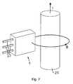
- Fig. 7
- eine Messvorrichtung zur Erfassung eines Messsignals, das dem elektrischen Strom in einem Leiter entspricht.
- Fig. 1
- a plan view of a first embodiment of a semiconductor chip, in which a measuring coil, a Hall sensor and a Signalverarbeitungseinrich device are monolithically integrated, the Hall plate of the Hall sensor and the signal processing means are shown only schematically,
- Fig. 2
- a plan view of a second embodiment of a semiconductor chip, in which a so-called vertical Hall plate is integrated,
- Fig. 3
- a measuring device in which the measuring coil and a semiconductor chip containing the Hall sensor and the signal processing device are arranged on a printed circuit board,
- Figure 4
- a further embodiment of the measuring device, in which the planes spanned by the windings of the measuring coil extend approximately orthogonal to the plane of extent of the printed circuit board,
- Fig. 5
- a cross section through a first embodiment of a position, speed and / or acceleration sensor,
- Figure 6
- a cross-section through a second embodiment of a position, speed and / or acceleration sensor, and
- Fig. 7
- a measuring device for detecting a measurement signal corresponding to the electric current in a conductor.
Eine in
Die Messspule 3 hat an ihren Enden erste elektrische Anschlüsse 5, an denen ein erstes Messsignal anliegt, das der bei einer Änderung des magnetischen Felds in der Messspule 3 induzierten elektrischen Spannung entspricht. Das erste erstes Messsignal ist gemäß den Induktionsgesetz etwa proportional zur Änderungsgeschwindigkeit des magnetischen Felds, weshalb in dem magnetischen Feld enthaltene höherfrequente Signalanteile in dem Messsignal stärker repräsentiert sind, als niederfrequente Signalanteile. Ein eventueller in dem magnetischen Feld enthaltener Gleichanteil verursacht kein Messsignal an der Messspule 3.The measuring
Der Hallsensor 4 weist eine Hallplatte 6 auf, an der zwei voneinander beabstandete zweite elektrische Anschlüsse 7 vorgesehen sind, in die ein Konstantstrom eingespeist wird, der von einer in der Zeichnung nicht näher dargestellten Messstromquelle bereitgestellt wird. An der Hallplatte 6 sind ferner dritte elektrische Anschlüsse 8 zum Abgreifen einer durch das magnetische Feld bewirkten Hallspannung vorgesehen. Die Hallspannung wird nachstehend auch als zweites Messsignal bezeichnet, In dem zweiten Messsignal sind sowohl ein in dem magnetischen Feld enthaltener Gleichanteil als auch ein Wechselanteil berücksichtigt. Mit zunehmender Frequenz des magnetischen Felds nimmt jedoch das zweite Messsignal ab.The
Die ersten elektrischen Anschlüsse 6 und die dritten elektrischen Anschlüsse 8 sind jeweils mit einem Eingang einer Signalverarbeitungseinrichtung 9 verbunden, die als elektrische Schaltung monolithisch in den Halbleiterchip 2 integriert ist. Die Signalverarbeitungseinrichtung 9 erzeugt in Abhängigkeit von dem ersten Messsignal und dem zweiten Messsignal ein dem magnetischen Feld entsprechendes Ausgangssignal, das an einem Ausgang 10 abgreifbar ist. In dem Ausgangssignal sind der Gleichanteil des magnetischen Felds sowie niederfrequente und hochfrequente Anteile gleichermaßen berücksichtigt, so dass sich eine über einen weiten Frequenzbereich nahezu linearer Frequenzgang ergibt.The first electrical connections 6 and the third electrical connections 8 are each connected to an input of a
In
Die Messspule 3 hat zwei parallel zueinander beabstandete Leiterbahnebenen. Die Leiterbahnen 12a einer ersten Leiterbahnebene sind in der Zeichnung als durchgezogene Linie und die Leiterbahnen 12b einer zweiten Leiterbahnebene als strichlinierte Linien dargestellt. Deutlich ist erkennbar, dass die Leiterbahnen 12a der ersten Leiterbahnebene in der Aufsicht auf den Halbleiterchip 2 etwa rechtwinklig zu den Leiterbahnen 12b der zweiten Leiterbahnebene verlaufen. Die Leiterbahnen 12a, 12b der unterschiedlichen Leiterbahnebene sind durch Durchkontaktierungen miteinander verbunden.The measuring
Der Hallsensor 4 oder dessen orthogonale Projektion auf die Erstreckungsebene der Messspule 3 ist innerhalb der Messspule 3 in dem von der innersten Windung umgrenzten Raum angeordnet. Die Verbindungsleiterbahnen 14 zwischen der Hallplatte 6 und der Signalverarbeitungseinrichtung verlaufen in der ersten Leiterbahnebene zwischen den Leiterbahnen 12a.The
Bei dem in
Die Messspule 3 hat zwei parallel zueinander beabstandete Leiterbahnebenen. Die Leiterbahnen 12a einer ersten Leiterbahnebene sind in der Zeichnung als durchgezogene Linie und die Leiterbahnen 12b einer zweiten Leiterbahnebene sowie die Durchkontaktierungen 13 sind jeweils als strichlinierte Linien dargestellt. Die Leiterbahnen 12a der ersten Leiterbahnebene verlaufen etwa parallel zu den Leiterbahnen 12b der zweiten Leiterbahnebene.The measuring
Bei dem in
Bei dem in
Der Halbleiterchip 2 ist über der Messspule 3 auf dem Träger 15 angeordnet. Die Ebene, in der sich der Halbleiterchip 2 erstreckt, verläuft etwa parallel zur Erstreckungsebene des Trägers 15. Wie bei dem Ausführungsbeispiel gemäß
Die Messvorrichtung 1 kann in einem Lage-, Geschwindigkeits- und/oder Beschleunigungssensor 19 angeordnet sein. Diese hat einen relativ zu der Messvorrichtung 1 in Richtung des Doppelpfeils 20 bewegbar gelagerten Geber 17, der bei dem in
Die Magnetpole 18 sind an der Messvorrichtung 1 vorbei bewegbar und verursachen dabei einen magnetischen Wechselfluss, der die Messspule 3 und die Hallplatte 6 jeweils etwa orthogonal zu deren Erstreckungsebene durchsetzen. In dem Ausgangssignal der Signalverarbeitungseinrichtung 9 wird bei jedem Vorbeibewegen eines Magnetpols 18 an der Messvorrichtung 1 ein Impuls oder eine Impulslücke erzeugt, und zwar auch dann, wenn sich die Magnetpole 18 mit sehr geringer oder mit hoher Geschwindigkeit an der Messvorrichtung 1 vorbeibewegen.The
In
Bei dem Lage-, Geschwindigkeits- und/oder Beschleunigungssensor 19 gemäß
Bei dem in
Claims (12)
Priority Applications (3)
| Application Number | Priority Date | Filing Date | Title |
|---|---|---|---|
| EP07017942A EP2037286A1 (en) | 2007-09-13 | 2007-09-13 | Measuring device for measuring a magnetic field |
| JP2008229219A JP2009069148A (en) | 2007-09-13 | 2008-09-08 | Device for measuring magnetic field |
| US12/209,625 US8067934B2 (en) | 2007-09-13 | 2008-09-12 | Measurement device for measuring a magnetic field |
Applications Claiming Priority (1)
| Application Number | Priority Date | Filing Date | Title |
|---|---|---|---|
| EP07017942A EP2037286A1 (en) | 2007-09-13 | 2007-09-13 | Measuring device for measuring a magnetic field |
Publications (1)
| Publication Number | Publication Date |
|---|---|
| EP2037286A1 true EP2037286A1 (en) | 2009-03-18 |
Family
ID=38969959
Family Applications (1)
| Application Number | Title | Priority Date | Filing Date |
|---|---|---|---|
| EP07017942A Withdrawn EP2037286A1 (en) | 2007-09-13 | 2007-09-13 | Measuring device for measuring a magnetic field |
Country Status (3)
| Country | Link |
|---|---|
| US (1) | US8067934B2 (en) |
| EP (1) | EP2037286A1 (en) |
| JP (1) | JP2009069148A (en) |
Cited By (1)
| Publication number | Priority date | Publication date | Assignee | Title |
|---|---|---|---|---|
| CN111208454A (en) * | 2020-01-09 | 2020-05-29 | 河北工业大学 | Hall-coil combined type three-dimensional magnetic characteristic measurement sensing box |
Families Citing this family (13)
| Publication number | Priority date | Publication date | Assignee | Title |
|---|---|---|---|---|
| DE102009029528A1 (en) * | 2009-09-17 | 2011-03-24 | Robert Bosch Gmbh | Integrated circuit for information transmission |
| KR20120040040A (en) * | 2010-10-18 | 2012-04-26 | 삼성전기주식회사 | Integrated apparatus for sensing current |
| FR2982032B1 (en) * | 2011-11-02 | 2013-11-08 | Univ Nancy 1 Henri Poincare | SURVEILLANCE APPARATUS IN A MAGNETIC ENVIRONMENT AND ASSOCIATED METHOD |
| JP2015146723A (en) * | 2014-01-06 | 2015-08-13 | 日東電工株式会社 | Wireless power transmitter |
| CN104219613B (en) * | 2014-03-20 | 2017-11-10 | 江苏多维科技有限公司 | A kind of magneto-resistor audio collection device |
| KR101873855B1 (en) * | 2015-02-23 | 2018-07-03 | 한국전자통신연구원 | Triaxial sensor and device including the same for measuring magnetic field |
| CN105182254B (en) * | 2015-07-31 | 2018-01-05 | 江汉大学 | Static weak magnetic field testing device |
| CN105172840A (en) * | 2015-09-29 | 2015-12-23 | 沧州师范学院 | Device and method for detecting close contact between circuit board and turnout |
| US11378468B2 (en) * | 2016-08-12 | 2022-07-05 | Brightsentinel Limited | Sensor module and process for producing same |
| US10607925B2 (en) * | 2017-10-06 | 2020-03-31 | Allegro Microsystems, Llc | Integrated circuit package having a raised lead edge |
| TWI635289B (en) * | 2017-11-17 | 2018-09-11 | 財團法人工業技術研究院 | Sensing method for power consumption and sensing device |
| CN113167595A (en) * | 2018-12-13 | 2021-07-23 | 海拉有限双合股份公司 | Sensor arrangement comprising two different types of rotation angle sensors |
| CN112904127A (en) * | 2021-01-26 | 2021-06-04 | 浙江亚太机电股份有限公司 | Low-frequency magnetic field interference generating device |
Citations (5)
| Publication number | Priority date | Publication date | Assignee | Title |
|---|---|---|---|---|
| DE69802203T2 (en) | 1997-04-21 | 2002-06-27 | Arbeitsgemeinschaft Prof Dr J | DEVICE WITH A BANDPASS WIDE BANDWIDTH FOR MEASURING ELECTRICAL CURRENT STRENGTH IN ONE LADDER |
| EP1314993A2 (en) * | 2001-11-23 | 2003-05-28 | Robert Bosch Gmbh | Device for measuring a magnetic field and measuring a current |
| DE10314602A1 (en) * | 2003-03-31 | 2004-10-21 | Infineon Technologies Ag | Monolithically integrated differential magnetic field sensor device, has layer of permeable material covering two magnetic field sensor elements, parallel to substrate |
| WO2006034551A1 (en) * | 2004-09-28 | 2006-04-06 | The University Of Queensland | Magnetic field dosimeter |
| EP1746430A1 (en) * | 2005-07-22 | 2007-01-24 | Liaisons Electroniques-Mecaniques Lem S.A. | Orthogonal fluxgate magnetic field sensor |
Family Cites Families (11)
| Publication number | Priority date | Publication date | Assignee | Title |
|---|---|---|---|---|
| JPS57104284A (en) * | 1980-12-19 | 1982-06-29 | Sharp Corp | Magnetic coupling element |
| JPH08264857A (en) * | 1995-01-26 | 1996-10-11 | Matsushita Electric Works Ltd | Integrated isolator |
| EP1031493B1 (en) | 1997-11-12 | 2006-08-02 | JTEKT Corporation | A steering device for vehicles |
| TW448528B (en) | 1998-08-29 | 2001-08-01 | Chen Yann Yann | Inductor inside hall sensor |
| TW434598B (en) | 1999-04-12 | 2001-05-16 | Chung Shan Inst Of Science | Enhancement Hall sensor |
| DE60002319T2 (en) | 1999-05-25 | 2004-02-12 | Arbeitsgemeinschaft Prof. Hugel Agph | ELECTRIC CURRENT SENSOR |
| US6566855B1 (en) * | 2001-04-20 | 2003-05-20 | Neilsen-Kuljian, Inc. | Current sensor with frequency output |
| DE20119163U1 (en) | 2001-11-26 | 2002-03-07 | Hindermann Gmbh & Co Kg | Protective cover for vehicles |
| JP4244766B2 (en) * | 2003-09-30 | 2009-03-25 | 株式会社デンソー | Multi-axis magnetic sensor |
| JP2005172441A (en) * | 2003-12-08 | 2005-06-30 | Yaskawa Electric Corp | Angle and angular velocity integrated detector |
| US7164263B2 (en) * | 2004-01-16 | 2007-01-16 | Fieldmetrics, Inc. | Current sensor |
-
2007
- 2007-09-13 EP EP07017942A patent/EP2037286A1/en not_active Withdrawn
-
2008
- 2008-09-08 JP JP2008229219A patent/JP2009069148A/en active Pending
- 2008-09-12 US US12/209,625 patent/US8067934B2/en active Active
Patent Citations (5)
| Publication number | Priority date | Publication date | Assignee | Title |
|---|---|---|---|---|
| DE69802203T2 (en) | 1997-04-21 | 2002-06-27 | Arbeitsgemeinschaft Prof Dr J | DEVICE WITH A BANDPASS WIDE BANDWIDTH FOR MEASURING ELECTRICAL CURRENT STRENGTH IN ONE LADDER |
| EP1314993A2 (en) * | 2001-11-23 | 2003-05-28 | Robert Bosch Gmbh | Device for measuring a magnetic field and measuring a current |
| DE10314602A1 (en) * | 2003-03-31 | 2004-10-21 | Infineon Technologies Ag | Monolithically integrated differential magnetic field sensor device, has layer of permeable material covering two magnetic field sensor elements, parallel to substrate |
| WO2006034551A1 (en) * | 2004-09-28 | 2006-04-06 | The University Of Queensland | Magnetic field dosimeter |
| EP1746430A1 (en) * | 2005-07-22 | 2007-01-24 | Liaisons Electroniques-Mecaniques Lem S.A. | Orthogonal fluxgate magnetic field sensor |
Non-Patent Citations (3)
| Title |
|---|
| CHUCHENG XIAO ET AL: "An overview of integratable current sensor technologies", CONFERENCE RECORD OF THE 2003 IEEE INDUSTRY APPLICATIONS CONFERENCE. 38TH. IAS ANNUAL MEETING . SALT LAKE CITY, UT, OCT. 12 - 16, 2003, CONFERENCE RECORD OF THE IEEE INDUSTRY APPLICATIONS CONFERENCE. IAS ANNUAL MEETING, NEW YORK, NY : IEEE, US, vol. VOL. 3 OF 3. CONF. 38, 12 October 2003 (2003-10-12), pages 1251 - 1258, XP010675997, ISBN: 0-7803-7883-0 * |
| DALESSANDRO L; KARRER N; KOLAR J W: "A Novel Isolated Current Sensor for High-Performance Power Electronics Applications", APEC 2006. TWENTY-FIRST ANNUAL IEEE APPLIED POWER ELECTRONICS CONFERENCE AND EXPOSITION, 19 March 2006 (2006-03-19) - 23 March 2006 (2006-03-23), Piscataway, NJ, USA, pages 559 - 566, XP002467118 * |
| DALESSANDRO, L; KARRER, N.; KOLAR, J. W.: "A Novel Isolated Current Sensor fbr High-Performance Power Electronics Apllications", APEC 2006, TWENTYFIRST ANNUAL IEEE APPLIED POWER ELECTRONICS CONFERENCE AND EXPOSITION, 19 March 2006 (2006-03-19), pages 559 - 566 |
Cited By (1)
| Publication number | Priority date | Publication date | Assignee | Title |
|---|---|---|---|---|
| CN111208454A (en) * | 2020-01-09 | 2020-05-29 | 河北工业大学 | Hall-coil combined type three-dimensional magnetic characteristic measurement sensing box |
Also Published As
| Publication number | Publication date |
|---|---|
| US20090140726A1 (en) | 2009-06-04 |
| US8067934B2 (en) | 2011-11-29 |
| JP2009069148A (en) | 2009-04-02 |
Similar Documents
| Publication | Publication Date | Title |
|---|---|---|
| EP2037286A1 (en) | Measuring device for measuring a magnetic field | |
| EP2063229B1 (en) | Magnetic field sensor system | |
| EP0226574B1 (en) | Magnetoresistive sensor for producing electric signals | |
| DE102004010126B4 (en) | Magnetic field sensor and method for producing the same | |
| EP1110094B1 (en) | Device and method for creating one or more magnetic field gradients through a straight conductor | |
| EP2564164B1 (en) | Magnetic length measuring system, length measuring method and method for producing a magnetic length measuring system | |
| DE102015001553B3 (en) | sensor device | |
| DE102008059775A1 (en) | Absolutely measuring steering angle sensor arrangement | |
| EP0726448A1 (en) | Magnetic position sensor | |
| EP1475604A2 (en) | Inductive angle sensor | |
| DE102012223037A1 (en) | Inductive position measuring device | |
| EP3495781A1 (en) | Inductive position measurement device | |
| EP3936828B1 (en) | Encoding system for a transmission | |
| DE102006038162A1 (en) | Electric motor with measuring system for position or movement | |
| EP2149784B1 (en) | Magnetic path sensor system | |
| DE102021210910A1 (en) | SCANNING ELEMENT AND INDUCTIVE POSITION MEASUREMENT DEVICE WITH THIS SCANNING ELEMENT | |
| DE19647420B4 (en) | Device for detecting a magnetic field | |
| DE102006024150A1 (en) | Planar direct drive with improved position determination and sensor unit for this | |
| WO2016150616A1 (en) | Sensor arrangement for measuring the rate of rotation of a rotating component | |
| DE19525292C2 (en) | Device for detecting the angle of rotation, the speed and / or the direction of rotation of a rotary drive | |
| DE102012221327A1 (en) | Sensor device for use in sensor system for determining rotational characteristic of rotating element, has transmitter wheel connected with rotating element, where transmitter wheel has multiple magnetic event detectors | |
| DE19731555B4 (en) | Magnetic position sensor | |
| DE4442441C2 (en) | Miniaturized coil arrangement manufactured in planar technology for the detection of ferromagnetic substances | |
| AT520709B1 (en) | Electromagnetic measuring system for the detection of length and angle based on the magnetoimpedance effect | |
| DE102006000470A1 (en) | Electromechanical conversion device |
Legal Events
| Date | Code | Title | Description |
|---|---|---|---|
| PUAI | Public reference made under article 153(3) epc to a published international application that has entered the european phase |
Free format text: ORIGINAL CODE: 0009012 |
|
| AK | Designated contracting states |
Kind code of ref document: A1 Designated state(s): AT BE BG CH CY CZ DE DK EE ES FI FR GB GR HU IE IS IT LI LT LU LV MC MT NL PL PT RO SE SI SK TR |
|
| AX | Request for extension of the european patent |
Extension state: AL BA HR MK RS |
|
| 17P | Request for examination filed |
Effective date: 20090520 |
|
| AKX | Designation fees paid |
Designated state(s): DE |
|
| STAA | Information on the status of an ep patent application or granted ep patent |
Free format text: STATUS: THE APPLICATION HAS BEEN WITHDRAWN |
|
| 18W | Application withdrawn |
Effective date: 20130328 |