JP2009290843A - Signal transmission apparatus - Google Patents
Signal transmission apparatus Download PDFInfo
- Publication number
- JP2009290843A JP2009290843A JP2008144370A JP2008144370A JP2009290843A JP 2009290843 A JP2009290843 A JP 2009290843A JP 2008144370 A JP2008144370 A JP 2008144370A JP 2008144370 A JP2008144370 A JP 2008144370A JP 2009290843 A JP2009290843 A JP 2009290843A
- Authority
- JP
- Japan
- Prior art keywords
- signal
- transmission
- differential
- circuit
- phase
- Prior art date
- Legal status (The legal status is an assumption and is not a legal conclusion. Google has not performed a legal analysis and makes no representation as to the accuracy of the status listed.)
- Granted
Links
Images


Abstract
Description
この発明は、2本の伝送線路からなる1対の伝送線路を用いて、差動信号と同相信号とを同時に伝送する信号伝送装置に関する。 The present invention relates to a signal transmission device that simultaneously transmits a differential signal and an in-phase signal using a pair of transmission lines composed of two transmission lines.
データ伝送を行う方法として、複数本の伝送線路を用いて、1度に複数ビットのデータを伝送するパラレル伝送と、1本の伝送線路を用いて、1ビットずつ順番にデータを伝送するシリアル伝送とが知られている。
近年では、伝送速度の高速化に伴い、パラレル伝送において、伝送線路数が増加したり、伝送線路間にスキューが発生したりするという問題点が顕著になっている。そのため、高速伝送については、シリアル伝送が多く用いられている。
As a method of data transmission, parallel transmission that transmits multiple bits of data at once using multiple transmission lines and serial transmission that transmits data one bit at a time using one transmission line Is known.
In recent years, with the increase in transmission speed, problems such as an increase in the number of transmission lines and occurrence of skew between transmission lines have become prominent in parallel transmission. Therefore, serial transmission is often used for high-speed transmission.
また、特に電磁環境両立性(EMC:Electro−Magnetic Compatibility)の観点から、シリアル伝送の中でも、2本の伝送線路を1対として、それぞれの伝送線路に対して互いに逆相の信号(差動信号)を伝送することによってデータ伝送を行う差動伝送が多く用いられている。
ここで、差動伝送では、差動信号が電磁界的に互いに結合して伝送されるので、外部への不要輻射が少なくなるという特徴がある。また、外部からのノイズは、同相信号として1対の伝送線路に重畳するが、差動伝送では、受信時に2本の伝送線路の信号の差分をデータとして取り出すので、同相成分であるノイズが相殺されるという特徴がある。
In particular, from the viewpoint of electromagnetic compatibility (EMC: Electro-Magnetic Compatibility), among serial transmissions, two transmission lines are paired, and signals of opposite phases to each transmission line (differential signals). ) Is often used for data transmission by transmitting data.
Here, the differential transmission has a feature that unnecessary radiation to the outside is reduced because the differential signals are electromagnetically coupled to each other and transmitted. In addition, noise from the outside is superimposed on a pair of transmission lines as an in-phase signal, but in differential transmission, the difference between the signals of the two transmission lines is extracted as data during reception. There is a feature that it is offset.
なお、データ伝送では、受信の際に各ビットを正確に取り込むためのタイミングクロックが必要になる。パラレル伝送では、データ信号用の伝送線路とは別にクロック線を設け、クロック線を用いてクロック信号を直接伝送する方法が一般的である。
これに対して、シリアル伝送では、伝送線路数の増加を避けるために、クロック線を設けてクロック信号を伝送するのではなく、ある一定の割合以上で必ず信号の変化が起こるようにデータを符号化し、受信側で信号の変化タイミングを検出することにより、クロックを再生する方法(CDR:Clock Data Recovery)が用いられている。
In data transmission, a timing clock is required to accurately capture each bit at the time of reception. In parallel transmission, a method of providing a clock line separately from a transmission line for data signals and directly transmitting a clock signal using the clock line is generally used.
On the other hand, in serial transmission, in order to avoid an increase in the number of transmission lines, a clock signal is not transmitted by providing a clock line, but data is encoded such that a signal change always occurs at a certain rate or more. And a method of regenerating the clock (CDR: Clock Data Recovery) by detecting the signal change timing on the receiving side.
クロック線を用いてクロック信号を直接伝送する場合には、クロック線の他に、信号の帰還線路となるリターン線が必要になる。このとき、シングルエンド信号のパラレル伝送やシリアル伝送の場合であれば、グランド線とも呼ばれるリターン線が、データ信号用にもとから設けられているので、クロック信号用の伝送線路を1本追加すればよい。
しかしながら、差動信号のシリアル伝送の場合には、互いに逆相の信号が伝送されるので、リターン線が不要となり設けられていない。そのため、クロックをシングルエンド信号として伝送する場合も、差動信号として伝送する場合も、2本の伝送線路を追加する必要がある。この場合には、データ信号用の2本の伝送線路に加えて、クロック信号用の2本の伝送線路を追加することとなり、伝送線路の数が倍増してコストが上がるとともに、構成が複雑になるという問題点があった。
When a clock signal is directly transmitted using a clock line, a return line serving as a signal feedback line is required in addition to the clock line. At this time, in the case of parallel transmission or serial transmission of a single-ended signal, a return line, also called a ground line, is originally provided for the data signal, so one transmission line for the clock signal is added. That's fine.
However, in the case of serial transmission of differential signals, signals with opposite phases are transmitted, and thus a return line is unnecessary and is not provided. Therefore, it is necessary to add two transmission lines both when transmitting the clock as a single-ended signal and when transmitting the clock as a differential signal. In this case, in addition to the two transmission lines for the data signal, two transmission lines for the clock signal are added, the number of transmission lines is doubled, the cost is increased, and the configuration is complicated. There was a problem of becoming.
また、受信側でクロックを再生する場合には、クロックを再生するために、データ伝送に先立ってクロック再生用の信号(プリアンブル)を伝送する必要がある。そのため、例えばフレーム長が短く分割されている場合には、データ伝送効率が低下するという問題点があった。また、複数(3台以上)の信号伝送装置が接続されて相互にデータ伝送を行うマルチポイント接続の場合には、送信装置が切り替わるたびにクロックを再生するための時間が必要となり、さらにデータ伝送効率が低下するという問題点があった。
また、1度再生されたクロックも、そのタイミングの維持または追従のために、一定の割合以上の頻度で信号の変化が起こるようにデータを符号化する必要がある。そのため、この符号化により、本来のデータのビット量よりも多くのビット量のデータを伝送することになり、データ伝送効率がさらに低下するという問題点があった。
When the clock is regenerated on the receiving side, it is necessary to transmit a clock regenerating signal (preamble) prior to data transmission in order to regenerate the clock. Therefore, for example, when the frame length is short and divided, there is a problem that the data transmission efficiency is lowered. In addition, in the case of multipoint connection in which a plurality of (three or more) signal transmission apparatuses are connected to perform data transmission with each other, it takes time to regenerate the clock every time the transmission apparatus is switched. There was a problem that efficiency decreased.
In addition, in order to maintain or follow the timing of the once regenerated clock, it is necessary to encode data so that the signal changes at a frequency of a certain rate or more. For this reason, this encoding has a problem in that data having a bit amount larger than the original bit amount is transmitted, and the data transmission efficiency is further reduced.
そこで、これらの問題点を解決するために、データを差動信号として伝送する2本で1対の伝送線路(以下、「ペア線路」と称する)に、クロックを同相信号として重畳し、異なる信号を同じ伝送線路で伝送することが考えられる。
異なる信号を同じ伝送線路で伝送する発明としては、例えば以下のものが挙げられる。
Therefore, in order to solve these problems, a clock is superimposed as an in-phase signal on two pairs of transmission lines (hereinafter referred to as “pair lines”) that transmit data as differential signals, and are different. It is conceivable to transmit the signal through the same transmission line.
Examples of the invention for transmitting different signals through the same transmission line include the following.
従来の信号伝送システムは、1対の伝送線路(ペア線路)のそれぞれの終端抵抗の中間電位点に接続されたシングルエンド送受信回路を備えている。シングルエンド送受信回路からシングルエンド信号として出力されたクロックは、同相信号としてペア線路に重畳され、差動送受信回路から出力された差動信号とともにペア線路を伝送される(例えば、特許文献1参照)。
このように、ペア線路を用いて差動信号と同相信号とを伝送することにより、伝送線路の数を倍増させることなく、また、データ伝送効率を下げることなく差動信号と同相信号とを伝送することができる。
A conventional signal transmission system includes a single-end transmission / reception circuit connected to an intermediate potential point of each termination resistor of a pair of transmission lines (pair lines). The clock output from the single-end transmission / reception circuit as a single-end signal is superimposed on the pair line as an in-phase signal, and transmitted along the pair line together with the differential signal output from the differential transmission / reception circuit (for example, see Patent Document 1). ).
Thus, by transmitting a differential signal and an in-phase signal using a pair line, the differential signal and the in-phase signal can be transmitted without doubling the number of transmission lines and without reducing the data transmission efficiency. Can be transmitted.
しかしながら、従来技術には、次のような問題点があった。
従来の信号伝送システムにおいて、シングルエンド送受信回路は、ペア線路の終端抵抗の中間電位点に直接接続され、差動送受信回路は、ペア線路に直接接続されている。そのため、例えば差動信号送信回路およびシングルエンド送受信回路がともに信号を送信している場合には、ともにインピーダンスが低い状態となり、差動送受信回路から送信された差動信号の一部が、ペア線路の反対側の差動送受信回路に受信されることなく、シングルエンド送受信回路に受信される恐れがある。また、同様に、シングルエンド送受信回路から送信されたシングルエンド信号の一部が、ペア線路の反対側のシングルエンド送受信回路に受信されることなく、差動送受信回路に受信される恐れもある。
すなわち、従来の信号伝送システムでは、差動信号と同相信号(シングルエンド信号)とが十分にペア線路に伝送されないという問題点があった。
However, the prior art has the following problems.
In the conventional signal transmission system, the single-end transmission / reception circuit is directly connected to the intermediate potential point of the termination resistance of the pair line, and the differential transmission / reception circuit is directly connected to the pair line. Therefore, for example, when the differential signal transmission circuit and the single-end transmission / reception circuit both transmit signals, both impedances are in a low state, and a part of the differential signal transmitted from the differential transmission / reception circuit is a pair line. There is a possibility that the signal is received by the single-end transmitting / receiving circuit without being received by the differential transmitting / receiving circuit on the opposite side. Similarly, a part of the single end signal transmitted from the single end transmission / reception circuit may be received by the differential transmission / reception circuit without being received by the single end transmission / reception circuit on the opposite side of the pair line.
That is, the conventional signal transmission system has a problem that the differential signal and the in-phase signal (single end signal) are not sufficiently transmitted to the pair line.
また、同相信号を伝送する場合には、信号の帰還線路となるリターン線が必要になるが、従来の信号伝送システムでは、リターン線の構成が明確に示されていないので、同相信号を伝送できない恐れがあるという問題点もあった。
また、従来の信号伝送システムでは、シングルエンド送受信回路を終端抵抗の中間電位点に接続して同相信号を伝送しているので、複数(3台以上)の信号伝送装置が接続されたマルチポイント接続の場合には、ペア線路間の抵抗値が低下し、電位差が減少する。そのため、従来の信号伝送システムは、3台以上のデータ伝送に適応しないという問題点もあった。
In addition, when transmitting an in-phase signal, a return line as a signal feedback line is required. However, in the conventional signal transmission system, the configuration of the return line is not clearly shown. There was also a problem that transmission could not be performed.
Moreover, in the conventional signal transmission system, a single-end transmission / reception circuit is connected to the intermediate potential point of the terminating resistor to transmit the in-phase signal, so that a multipoint in which a plurality (three or more) of signal transmission devices are connected. In the case of connection, the resistance value between the pair lines decreases, and the potential difference decreases. For this reason, the conventional signal transmission system has a problem that it is not suitable for data transmission of three or more units.
この発明は、上記のような課題を解決するためになされたものであって、その目的は、差動信号と同相信号とを分離して、差動信号と同相信号とを、1対の伝送線路を用いて確実に伝送するとともに、マルチポイント接続に対応することができる信号伝送装置を提供することにある。 The present invention has been made to solve the above-described problems, and an object of the present invention is to separate a differential signal and an in-phase signal into a pair of the differential signal and the in-phase signal. An object of the present invention is to provide a signal transmission device that can reliably transmit using a transmission line and can support multipoint connection.
この発明に係る信号伝送装置は、2本の伝送線路からなる1対の伝送線路を用いて、1対の差動信号、および1対の同相信号として重畳されたシングルエンド信号を伝送する信号伝送装置であって、1対の伝送線路から分岐して接続され、差動信号と同相信号とを送受信する送受信装置を備え、送受信装置は、差動信号と同相信号とを分離または合成して出力する分離合成回路と、分離合成回路との間で差動信号を送受信する差動送受信バッファと、分離合成回路との間でシングルエンド信号を送受信するシングルエンド送受信バッファとを備え、分離合成回路は、差動信号に対して低インピーダンスとなり、同相信号に対して高インピーダンスとなることにより、差動信号を通過させる差動信号通過手段と、同相信号に対して低インピーダンスとなり、差動信号に対して高インピーダンスとなることにより、同相信号を通過させる同相信号通過手段とを含むものである。 The signal transmission device according to the present invention uses a pair of transmission lines composed of two transmission lines to transmit a pair of differential signals and a single-ended signal superimposed as a pair of in-phase signals. A transmission device comprising a transmission / reception device that is branched and connected from a pair of transmission lines and transmits / receives a differential signal and an in-phase signal, and the transmission / reception device separates or combines the differential signal and the in-phase signal. Separate separation / synthesis circuit, differential transmission / reception buffer that transmits / receives differential signals to / from the separation / synthesis circuit, and single-end transmission / reception buffer that transmits / receives single-ended signals to / from the separation / synthesis circuit. The synthesizing circuit has a low impedance for the differential signal and a high impedance for the in-phase signal, thereby allowing the differential signal passing means to pass the differential signal and the low impedance to the in-phase signal. Scan and will, by a high impedance to differential signals, is intended to include an in-phase signal passing means for passing the in-phase signal.
この発明の信号伝送装置によれば、1対の伝送線路から分岐して接続された送受信装置は、差動信号と同相信号とを分離または合成して出力する分離合成回路を有している。また、分離合成回路は、差動信号に対して低インピーダンスとなることにより、差動信号を通過させる差動信号通過手段と、同相信号に対して低インピーダンスとなることにより、同相信号を通過させる同相信号通過手段とを含んでいる。
そのため、差動信号と同相信号とを分離して、差動信号と同相信号とを、1対の伝送線路を用いて確実に伝送するとともに、マルチポイント接続に対応することができる。
According to the signal transmission device of the present invention, the transmission / reception device branched and connected from the pair of transmission lines has the separation / synthesis circuit for separating or synthesizing and outputting the differential signal and the in-phase signal. . In addition, the separation / combination circuit has a low impedance for the differential signal, so that the differential signal passing means for passing the differential signal, and the low impedance for the common mode signal, And in-phase signal passing means for passing.
Therefore, the differential signal and the in-phase signal can be separated, and the differential signal and the in-phase signal can be reliably transmitted using a pair of transmission lines, and multipoint connection can be supported.
以下、この発明の各実施の形態について図に基づいて説明するが、各図において同一、または相当する部分については、同一符号を付して説明する。
なお、以下の実施の形態では、差動信号がデータで、シングルエンド信号がクロックである場合を例に挙げて説明するが、これに限定されず、例えば差動信号が画像データで、シングルエンド信号が音声データであってもよい。
Hereinafter, embodiments of the present invention will be described with reference to the drawings. In the drawings, the same or corresponding parts will be described with the same reference numerals.
In the following embodiments, the case where the differential signal is data and the single-ended signal is a clock will be described as an example. However, the present invention is not limited to this. For example, the differential signal is image data and the single-ended signal is single-ended. The signal may be audio data.
実施の形態1.
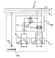
図1は、この発明の実施の形態1に係る信号伝送装置を示す回路図である。
図1において、この信号伝送装置は、1対の差動信号(ディファレンシャルモード)と1対の同相信号(コモンモード)とを伝送する2本の伝送線路1、2からなる1対の伝送線路3(以下、「ペア線路3」と称する)と、同相信号の帰還線路となるリターン線4と、ペア線路3から分岐して接続され、差動信号と同相信号とを送受信する複数の送受信装置5とを備えている。
Embodiment 1 FIG.
1 is a circuit diagram showing a signal transmission apparatus according to Embodiment 1 of the present invention.
In FIG. 1, this signal transmission device includes a pair of
送受信装置5は、同相信号とシングルエンド信号とを互換するとともに、差動信号と同相信号とを分離または合成して出力する分離合成回路6と、分離合成回路6との間で差動信号を送受信する差動送受信バッファ7と、分離合成回路6との間でシングルエンド信号を送受信するシングルエンド送受信バッファ8とを有している。
また、ペア線路3の端部には、終端抵抗9が設けられており、リターン線4は、送受信装置5の基準電位となるシグナルグランド10に接続されている。
また、複数の送受信装置5は、互いに同一の構成を有している。
The transmission /
A termination resistor 9 is provided at the end of the
The plurality of transmission /
以下、図2を参照しながら、送受信装置5の構成について詳細に説明する。
図2は、この発明の実施の形態1に係る送受信装置5を詳細に示す回路図である。
図2において、分離合成回路6は、コモンモードチョークコイル61(差動信号通過手段)と、ディファレンシャルチョークコイル62(同相信号通過手段)とを含んでいる。
コモンモードチョークコイル61は、差動信号に対して低インピーダンスとなり、同相信号に対して高インピーダンスとなることにより、差動信号を通過させる。また、ディファレンシャルチョークコイル62は、同相信号に対して低インピーダンスとなり、差動信号に対して高インピーダンスとなることにより、同相信号を通過させる。
Hereinafter, the configuration of the transmission /
FIG. 2 is a circuit diagram showing in detail the transmitting / receiving
In FIG. 2, the separation /
The common
差動送受信バッファ7は、差動信号を送信する差動送信バッファ71と、差動信号を受信する差動受信バッファ72とを含んでいる。
また、シングルエンド送受信バッファ8は、シングルエンド信号を送信するシングルエンド送信バッファ81と、シングルエンド信号を受信するシングルエンド受信バッファ82とを含んでいる。
The differential transmission / reception buffer 7 includes a
The single end transmission /
以下、上記構成の信号伝送装置において、送受信装置5がデータを送信する場合の動作について説明する。
まず、送信データは、差動送信バッファ71に入力され、差動信号として分離合成回路6に入力される。また、クロックは、シングルエンド送信バッファ81に入力され、シングルエンド信号として分離合成回路6に入力される。
Hereinafter, in the signal transmission apparatus having the above configuration, an operation when the transmission /
First, transmission data is input to the
続いて、分離合成回路6に入力されたシングルエンド信号は、同相信号に変換された後、差動信号と合成されてペア線路3に送信される。
ここで、コモンモードチョークコイル61は、上述したように、差動信号に対して低インピーダンスとなり、同相信号に対して高インピーダンスとなる。そのため、差動送信バッファ71とシングルエンド送信バッファ81とが同時に送信を行う場合に、コモンモードチョークコイル61は、差動信号を低インピーダンスでペア線路3に送信するとともに、同相信号が低インピーダンスとなっている差動送信バッファ71に流れ込まないようブロックする。
Subsequently, the single-ended signal input to the separation /
Here, as described above, the common
また、ディファレンシャルチョークコイル62は、上述したように、同相信号に対して低インピーダンスとなり、差動信号に対して高インピーダンスとなる。そのため、シングルエンド送信バッファ81と差動送信バッファ71とが同時に送信を行う場合に、ディファレンシャルチョークコイル62は、同相信号を低インピーダンスでペア線路3に送信するとともに、差動信号が低インピーダンスとなっているシングルエンド送信バッファ81に流れ込まないようブロックする。
これにより、差動信号と同相信号とが合成される。
Further, as described above, the
As a result, the differential signal and the in-phase signal are combined.
以下、上記構成の信号伝送装置において、送受信装置5がデータを受信する場合の動作について説明する。
送受信装置5から送信された差動信号および同相信号は、ペア線路3を伝送されて別の送受信装置5に受信され、分離合成回路6に入力される。
このとき、差動信号は、ペア線路3のみを通って伝送される。一方、同相信号は、リターン線4を帰還線路として伝送される。
また、ペア線路3の端部に設けられた終端抵抗9は、ペア線路3の特性インピーダンスと同一またはその近傍の抵抗値を有しており、信号の反射が防止される。
Hereinafter, in the signal transmission apparatus having the above configuration, an operation when the transmission /
The differential signal and the in-phase signal transmitted from the transmission /
At this time, the differential signal is transmitted only through the
Further, the terminating resistor 9 provided at the end of the
続いて、分離合成回路6に入力された差動信号および同相信号は、差動信号および同相信号に分離され、同相信号は、さらにシングルエンド信号に変換される。
ここで、コモンモードチョークコイル61は、ペア線路3を伝送された差動信号および同相信号のうち、同相信号をブロックし、差動信号のみを差動受信バッファ72に出力する。
また、ディファレンシャルチョークコイル62は、ペア線路3を伝送された差動信号および同相信号のうち、差動信号をブロックし、同相信号のみを差動受信バッファ72に出力する。
これにより、差動信号と同相信号とが分離される。
Subsequently, the differential signal and the in-phase signal input to the separation /
Here, the common
The
Thereby, the differential signal and the in-phase signal are separated.
分離された差動信号は、差動受信バッファ72に入力され、データが取り出される。また、シングルエンド信号に変換されたクロック信号は、シングルエンド受信バッファ82に入力され、クロックが取り出される。また、このクロックタイミングに基づいて、データが復元される。
The separated differential signal is input to the
この発明の実施の形態1に係る信号伝送装置によれば、送受信装置5は、差動信号と同相信号とを分離または合成して出力する分離合成回路6を有している。また、分離合成回路6は、差動信号を通過させるコモンモードチョークコイル61と、同相信号を通過させるディファレンシャルチョークコイル62とを含んでいる。
そのため、一方の送受信バッファに他方のモードの信号の影響を与えることなく差動信号と同相信号とを分離して、差動信号と同相信号とを、ペア線路3を用いて確実に伝送することができる。また、コモンモードチョークコイル61およびディファレンシャルチョークコイル62を用いることにより、簡素な構成で効率的に差動信号と同相信号とを合成および分離することができる。
According to the signal transmission device according to the first embodiment of the present invention, the transmission /
Therefore, the differential signal and the in-phase signal are separated from each other without affecting the signal of the other mode in one transmission / reception buffer, and the differential signal and the in-phase signal are reliably transmitted using the
また、差動信号と同相信号とを分離または合成して出力する分離合成回路6を有することにより、1本の伝送線路をリターン線4として追加するだけで、ペア線路3を用いて差動信号と同相信号とを同時に伝送することができる。
また、送受信装置5がペア線路3から分岐して接続されているので、ペア線路3に3台以上の送受信装置5が接続されたマルチポイント接続の双方向通信に適用することができる。
Further, by having the separation /
Further, since the transmission /
実施の形態2.
図3は、この発明の実施の形態2に係る送受信装置5Aを詳細に示す回路図である。
図3において、分離合成回路6Aは、図2に示した分離合成回路6に加えて、第1キャパシタ63と、第2キャパシタ64と、プルアップ抵抗65と、プルダウン抵抗66とを含んでいる。
その他の構成については、実施の形態1と同様であり、その説明は省略する。
FIG. 3 is a circuit diagram showing in detail a
In FIG. 3, the separating / combining
Other configurations are the same as those of the first embodiment, and the description thereof is omitted.
以下、分離合成回路6Aの詳細な構成および機能について説明する。なお、コモンモードチョークコイル61およびディファレンシャルチョークコイル62については、上述した実施の形態1と同様なので、説明を省略する。
第1キャパシタ63は、ディファレンシャルチョークコイル62に設けられ、ペア線路3間に生じる直流的な短絡を防止する。
Hereinafter, a detailed configuration and function of the separation /
The
第2キャパシタ64は、ディファレンシャルチョークコイル62とシングルエンド送受信バッファ8との間に設けられ、シングルエンド信号の直流成分を除去する。
そのため、シングルエンド信号を送信する場合に、シングルエンド信号は、0Vを中心として振幅が変化する信号となり、シングルエンド信号のもつ不要なオフセットがペア線路3に伝わることを防止することができる。また、シングルエンド信号を受信する場合には、ペア線路3からの不要なオフセットが除去される。
The
Therefore, when a single end signal is transmitted, the single end signal becomes a signal whose amplitude changes around 0 V, and it is possible to prevent unnecessary offset of the single end signal from being transmitted to the
プルアップ抵抗65およびプルダウン抵抗66は、第2キャパシタ64とシングルエンド送受信バッファ8との接続点と、電源およびシグナルグランド10との間にそれぞれ設けられている。プルアップ抵抗65およびプルダウン抵抗66は、第2キャパシタ64により直流成分が除去されたシングルエンド信号の受信信号に対して、直流成分を付加する。
これにより、シングルエンド信号の受信信号は、0Vを中心電圧とした信号から、シングルエンド受信バッファ82の受信レベルに適合した中心電圧の信号に変換される。
The pull-up
Thereby, the reception signal of the single end signal is converted from the signal having 0V as the center voltage into the signal of the center voltage suitable for the reception level of the single
この発明の実施の形態2に係る信号伝送装置によれば、分離合成回路6Aは、第1キャパシタ63と第2キャパシタ64とを含んでいるので、シングルエンド送受信バッファ8とペア線路3との間で不要な直流成分を除去することができるとともに、ペア線路3間に生じる直流的な短絡を防止することができる。
また、分離合成回路6Aは、プルアップ抵抗65およびプルダウン抵抗66を含んでいるので、シングルエンド信号の受信信号を、シングルエンド受信バッファ82の受信レベルに適合した中心電圧の信号に変換することができる。
According to the signal transmission apparatus according to the second embodiment of the present invention, the separation /
Further, since the separation /
実施の形態3.
図4は、この発明の実施の形態3に係る送受信装置5Bを詳細に示す回路図である。
図4において、分離合成回路6Bは、図2に示した分離合成回路6に加えて、直列共振回路67を含んでいる。
その他の構成については、実施の形態1と同様であり、その説明は省略する。
FIG. 4 is a circuit diagram showing in detail a
In FIG. 4, the separation /
Other configurations are the same as those of the first embodiment, and the description thereof is omitted.
以下、分離合成回路6Bの詳細な構成および機能について説明する。なお、コモンモードチョークコイル61およびディファレンシャルチョークコイル62については、上述した実施の形態1と同様なので、説明を省略する。
直列共振回路67は、ディファレンシャルチョークコイル62とシングルエンド送受信バッファ8との間に設けられ、インダクタとキャパシタとを直列に接続した構成を有している。
Hereinafter, the detailed configuration and function of the separation /
The
ここで、インダクタとキャパシタとを直列に接続すると、特定の周波数帯域の信号に対して低インピーダンスとなり、その他の周波数帯域の信号に対して高インピーダンスとなる。すなわち、直列共振回路67は、バンドパスフィルタとして機能する。
そこで、同相信号であるクロック信号の周波数帯域を、直列共振回路67の通過帯域と適合させることにより、シングルエンド送受信バッファ8とペア線路3との間で、クロック信号成分のみが伝送される。
Here, when an inductor and a capacitor are connected in series, a low impedance is obtained for a signal in a specific frequency band, and a high impedance is obtained for a signal in another frequency band. That is, the
Therefore, only the clock signal component is transmitted between the single-ended transmission /
この発明の実施の形態3に係る信号伝送装置によれば、分離合成回路6Bは、直列共振回路67を含んでいるので、シングルエンド送受信バッファ8とペア線路3との間で不要な周波数帯域のノイズを除去して信号を伝送することができる。
なお、この実施の形態3に示した分離合成回路6Bを、上記実施の形態2で示した分離合成回路6Aと併用してもよい。
According to the signal transmission apparatus according to the third embodiment of the present invention, the separation /
Note that the separation /
実施の形態4.
図5は、この発明の実施の形態4に係る送受信装置5Cを詳細に示す回路図である。
図5において、分離合成回路6Cは、図2に示した分離合成回路6に加えて、並列共振回路68を含んでいる。
その他の構成については、実施の形態1と同様であり、その説明は省略する。
Embodiment 4 FIG.
FIG. 5 is a circuit diagram showing in detail a
In FIG. 5, the separation /
Other configurations are the same as those of the first embodiment, and the description thereof is omitted.
以下、分離合成回路6Cの詳細な構成および機能について説明する。なお、コモンモードチョークコイル61およびディファレンシャルチョークコイル62については、上述した実施の形態1と同様なので、説明を省略する。
並列共振回路68は、ディファレンシャルチョークコイル62とシングルエンド送受信バッファ8との接続点と、シグナルグランド10との間に設けられ、インダクタとキャパシタとを並列に接続した構成を有している。
Hereinafter, a detailed configuration and function of the separation /
The parallel
ここで、インダクタとキャパシタとを並列に接続すると、特定の周波数帯域の信号に対して高インピーダンスとなり、その他の周波数帯域の信号に対して低インピーダンスとなる。すなわち、並列共振回路68は、バンドエリミネーションフィルタとして機能する。
そこで、同相信号であるクロック信号の周波数帯域を、並列共振回路68の阻止帯域と適合させることにより、クロック信号の信号帯域外の信号成分を除去し、シングルエンド送受信バッファ8とペア線路3との間で、クロック信号成分のみが伝送される。
Here, when the inductor and the capacitor are connected in parallel, a high impedance is obtained for a signal in a specific frequency band, and a low impedance is obtained for signals in other frequency bands. That is, the
Therefore, by adapting the frequency band of the clock signal that is an in-phase signal to the stop band of the
この発明の実施の形態4に係る信号伝送装置によれば、分離合成回路6Cは、並列共振回路68を含んでいるので、シングルエンド送受信バッファ8とペア線路3との間で不要な周波数帯域のノイズを除去して信号を伝送することができる。
なお、この実施の形態4に示した分離合成回路6Cを、上記実施の形態2で示した分離合成回路6Aと併用してもよい。
According to the signal transmission apparatus according to the fourth embodiment of the present invention, the separation /
The separation /
実施の形態5.
図6は、この発明の実施の形態5に係る送受信装置5Dを詳細に示す回路図である。
図6において、分離合成回路6Dは、図2に示した分離合成回路6に加えて、絶縁トランス型共振回路69を含んでいる。
また、上記実施の形態1〜4では、リターン線4がシグナルグランド10に接続されているとしたが、この実施の形態5では、リターン線4は、送受信装置5Dの筐体や大地に接続されるフレームグランド11に接続されている。
その他の構成については、実施の形態1と同様であり、その説明は省略する。
FIG. 6 is a circuit diagram showing in detail a
In FIG. 6, the separation /
In the first to fourth embodiments, the return line 4 is connected to the
Other configurations are the same as those of the first embodiment, and the description thereof is omitted.
以下、分離合成回路6Dの詳細な構成および機能について説明する。なお、コモンモードチョークコイル61およびディファレンシャルチョークコイル62については、上述した実施の形態1と同様なので、説明を省略する。
絶縁トランス型共振回路69は、ディファレンシャルチョークコイル62と、シングルエンド送受信バッファ8と、シグナルグランド10と、フレームグランド11との間に設けられ、絶縁トランスとキャパシタとを並列に接続した構成を有している。また、絶縁トランスのペア線路3側の一方は、フレームグランド11に接続されたリターン線4に接続されている。
Hereinafter, a detailed configuration and function of the separation /
The insulation transformer
ここで、絶縁トランスとキャパシタとを並列に接続すると、ペア線路3とシングルエンド送受信バッファ8とが電気的に絶縁されるとともに、特定の周波数帯域の信号に対して高インピーダンスとなり、その他の周波数帯域の信号に対して低インピーダンスとなる。すなわち、絶縁トランス型共振回路69は、バンドエリミネーションフィルタとして機能する。
そこで、同相信号であるクロック信号の周波数帯域を、絶縁トランス型共振回路69の阻止帯域と適合させることにより、クロック信号の信号帯域外の信号成分を除去し、シングルエンド送受信バッファ8とペア線路3との間で、クロック信号成分のみが伝送される。
Here, when the isolation transformer and the capacitor are connected in parallel, the
Therefore, by adjusting the frequency band of the clock signal, which is an in-phase signal, to the stop band of the isolation transformer
この発明の実施の形態5に係る信号伝送装置によれば、分離合成回路6Dは、絶縁トランス型共振回路69を含んでいるので、シングルエンド送受信バッファ8とペア線路3との間で不要な周波数帯域のノイズを除去して信号を伝送することができる。
なお、この実施の形態5に示した分離合成回路6Dを、上記実施の形態2で示した分離合成回路6Aと併用してもよい。
According to the signal transmission apparatus according to the fifth embodiment of the present invention, the separation /
Note that the separation /
実施の形態6.
図7は、この発明の実施の形態6に係る送受信装置5Eを詳細に示す回路図である。
図7において、分離合成回路6Eは、図2に示した分離合成回路6に加えて、PLL回路70(PLL回路)を含んでいる。
その他の構成については、実施の形態1と同様であり、その説明は省略する。
FIG. 7 is a circuit diagram showing in detail a transmitting / receiving
In FIG. 7, the separation /
Other configurations are the same as those of the first embodiment, and the description thereof is omitted.
以下、分離合成回路6Eの詳細な構成および機能について説明する。なお、コモンモードチョークコイル61およびディファレンシャルチョークコイル62については、上述した実施の形態1と同様なので、説明を省略する。
PLL回路70は、ディファレンシャルチョークコイル62とシングルエンド受信バッファ82との間に設けられている。
一般的なPLL回路70は、図8に示すように、位相比較器、ループフィルタ、VCO(電圧制御発振器)および分周器を有している。なお、PLL回路70の構成は、図8のものに限定されない。
The detailed configuration and function of the separation /
The
As shown in FIG. 8, the
PLL回路70においては、ループフィルタの時定数によって応答速度を変えることができる。例えば、時定数を小さくすれば、クロック同期の時間を早くすることができ、時定数を大きくすれば、耐ノイズ性を高めることができる。
ここで、PLL回路70を用いることで、クロック信号の抽出とともに、クロック信号の分周または逓倍も同時に行うことができる。
In the
Here, by using the
この発明の実施の形態6に係る信号伝送装置によれば、分離合成回路6Eは、PLL回路70を含んでいるので、受信したクロック信号のノイズ成分を除去するとともに、ジッタを低減することができ、より確実なクロック信号を受信することができる。
なお、この実施の形態6に示した分離合成回路6Eを、上記実施の形態2で示した分離合成回路6Aと併用してもよい。
According to the signal transmission device according to the sixth embodiment of the present invention, since the separation /
Note that the separation /
なお、上記実施の形態1〜6では、同相信号を通過させる同相信号通過手段を、ディファレンシャルチョークコイル62としたが、これに限定されない。
例えば、図9に示すように、2個のインダクタ12を、ディファレンシャルチョークコイル62の代わりに用いてもよい。
In the first to sixth embodiments, the in-phase signal passing means for passing the in-phase signal is the
For example, as shown in FIG. 9, two
ここで、インダクタ12は、周波数の低い信号に対して低インピーダンスとなり、周波数の高い信号に対して高インピーダンスとなる。
そこで、同相信号であるクロック信号を、差動信号であるデータ信号よりも低い周波数帯域の信号とすることにより、2個のインダクタ12を用いて、同相信号のみを通過させることができ、ディファレンシャルチョークコイル62と同等の機能を実現することができる。
この場合には、ディファレンシャルチョークコイル62を用いるよりも安価かつ簡素な構成で、差動信号と同相信号とを合成および分離することができる。
Here, the
Therefore, by making the clock signal, which is an in-phase signal, a signal in a lower frequency band than the data signal, which is a differential signal, only the in-phase signal can be passed using the two
In this case, the differential signal and the in-phase signal can be synthesized and separated with a cheaper and simpler configuration than when the
また、上記実施の形態1〜6では、リターン線4として1本の伝送線路を追加していたが、これに限定されない。
例えば、図10に示すように、ペア線路3を外部電磁界から遮蔽するシールド13を、リターン線4の代わりに同相信号の帰還線路として用いてもよい。
この場合には、従来のシールド付伝送線路を用いて差動伝送を行う場合と同様に、2本の伝送線路のみを用いることにより、差動信号と同相信号とを同時に伝送することができる。
Moreover, in the said Embodiment 1-6, although one transmission line was added as the return line 4, it is not limited to this.
For example, as shown in FIG. 10, a
In this case, a differential signal and an in-phase signal can be transmitted simultaneously by using only two transmission lines, as in the case of performing differential transmission using a conventional shielded transmission line. .
また、上記実施の形態1〜6では、データを差動信号として伝送し、クロックをシングルエンド信号から同相信号に変換して伝送するとしたが、これに限定されず、データをシングルエンド信号から同相信号に変換して伝送し、クロックを差動信号として伝送してもよい。
また、上記実施の形態1〜6において、クロック信号は、必ずしもデータの最小変化周期に対応した信号である必要はなく、送信の際に分周した信号を送信し、受信後に逓倍してデータの復元に用いるなど、データの変化タイミングに同期したタイミング信号であってもよい。
また、上記実施の形態1〜6では、データ信号を送信する送受信装置5がクロック信号も同時に送信する構成となっている。しかしながら、これに限定されず、クロック信号を常に特定の送受信装置5から送信し、他の送受信装置5は常にクロック信号の受信のみを行う構成とし、それぞれシングルエンド送信バッファ81またはシングルエンド受信バッファ82の何れかのみを備えていてもよい。
これらの場合も、上記実施の形態1〜6と同様の効果を奏することができる。
In the first to sixth embodiments, data is transmitted as a differential signal, and a clock is converted from a single-ended signal to an in-phase signal. However, the present invention is not limited to this, and data is transmitted from a single-ended signal. The signal may be converted into an in-phase signal and transmitted, and the clock may be transmitted as a differential signal.
In the first to sixth embodiments, the clock signal does not necessarily need to be a signal corresponding to the minimum data change period. A signal divided at the time of transmission is transmitted, and after reception, the clock signal is multiplied to obtain the data It may be a timing signal synchronized with the data change timing, such as used for restoration.
In the first to sixth embodiments, the transmission /
In these cases, the same effects as those of the first to sixth embodiments can be obtained.
1、2 伝送線路、3 ペア線路、4 リターン線、5、5A〜5E 送受信装置、6、6A〜6E 分離合成回路、7 差動送受信バッファ、8 シングルエンド送受信バッファ、9 終端抵抗、10 シグナルグランド、11 フレームグランド、12 インダクタ、13 シールド、61 コモンモードチョークコイル(差動信号通過手段)、62 ディファレンシャルチョークコイル(同相信号通過手段)、63 第1キャパシタ、64 第2キャパシタ、65 プルアップ抵抗、66 プルダウン抵抗、67 直列共振回路、68 並列共振回路、69 絶縁トランス型共振回路、70 PLL回路(位相同期回路)、71 差動送信バッファ、72 差動受信バッファ、81 シングルエンド送信バッファ、82 シングルエンド受信バッファ。
1, 2 Transmission line, 3 Pair line, 4 Return line, 5, 5A-5E Transmitter / receiver, 6, 6A-6E Separation / synthesis circuit, 7 Differential transmission / reception buffer, 8 Single-end transmission / reception buffer, 9 Termination resistor, 10 Signal ground 11
Claims (9)
前記1対の伝送線路から分岐して接続され、前記差動信号と前記同相信号とを送受信する送受信装置を備え、
前記送受信装置は、
前記差動信号と前記同相信号とを分離または合成して出力する分離合成回路と、
前記分離合成回路との間で前記差動信号を送受信する差動送受信バッファと、
前記分離合成回路との間で前記シングルエンド信号を送受信するシングルエンド送受信バッファと、を備え、
前記分離合成回路は、
前記差動信号に対して低インピーダンスとなり、前記同相信号に対して高インピーダンスとなることにより、前記差動信号を通過させる差動信号通過手段と、
前記同相信号に対して低インピーダンスとなり、前記差動信号に対して高インピーダンスとなることにより、前記同相信号を通過させるとともに、前記同相信号と前記シングルエンド信号とを相互に変換する同相信号通過手段と、
を含むことを特徴とする信号伝送装置。 A signal transmission device that transmits a pair of differential signals and a single-ended signal superimposed as a pair of in-phase signals using a pair of transmission lines composed of two transmission lines,
A transmission / reception device that is branched and connected from the pair of transmission lines and that transmits and receives the differential signal and the in-phase signal,
The transmission / reception device includes:
A separating and synthesizing circuit for separating or synthesizing and outputting the differential signal and the in-phase signal;
A differential transmission / reception buffer for transmitting / receiving the differential signal to / from the separation / synthesis circuit;
A single-end transmission / reception buffer for transmitting / receiving the single-end signal to / from the separation / synthesis circuit,
The separation and synthesis circuit is
Differential signal passing means for passing the differential signal by having a low impedance for the differential signal and a high impedance for the in-phase signal;
The in-phase signal has a low impedance and the differential signal has a high impedance, thereby allowing the in-phase signal to pass through and converting the in-phase signal and the single-ended signal to each other. Phase signal passing means;
A signal transmission device comprising:
前記同相信号通過手段は、ディファレンシャルチョークコイルである
ことを特徴とする請求項1に記載の信号伝送装置。 The differential signal passing means is a common mode choke coil,
The signal transmission device according to claim 1, wherein the common-mode signal passing means is a differential choke coil.
前記差動信号通過手段は、コモンモードチョークコイルであり、
前記同相信号通過手段は、前記1対の同相信号の各々に対応する2個のインダクタである
ことを特徴とする請求項1に記載の信号伝送装置。 The in-phase signal is a signal having a lower frequency band than the differential signal,
The differential signal passing means is a common mode choke coil,
The signal transmission device according to claim 1, wherein the common-mode signal passing unit includes two inductors corresponding to each of the pair of common-mode signals.
前記同相信号通過手段に設けられ、前記2本の伝送線路の間の直流的な短絡を防止する第1キャパシタと、
前記同相信号通過手段と前記シングルエンド送受信バッファとの間に設けられ、前記シングルエンド信号の直流成分を除去する第2キャパシタと、
前記第2キャパシタと前記シングルエンド送受信バッファとの接続点と、電源およびグランドとの間にそれぞれ設けられ、前記第2キャパシタにより直流成分が除去された前記シングルエンド信号に、直流成分を付加するプルアップ抵抗およびプルダウン抵抗と、
をさらに有していることを特徴とする請求項1から請求項3までの何れか1項に記載の信号伝送装置。 The separation and synthesis circuit is
A first capacitor provided in the in-phase signal passing means and preventing a DC short circuit between the two transmission lines;
A second capacitor provided between the in-phase signal passing means and the single-ended transmission / reception buffer, for removing a DC component of the single-ended signal;
A pull-up circuit that is provided between a connection point between the second capacitor and the single-ended transmission / reception buffer, and a power source and a ground, and that adds a DC component to the single-ended signal from which the DC component has been removed by the second capacitor. Up and pull down resistors,
The signal transmission device according to any one of claims 1 to 3, further comprising:
Priority Applications (1)
| Application Number | Priority Date | Filing Date | Title |
|---|---|---|---|
| JP2008144370A JP5197164B2 (en) | 2008-06-02 | 2008-06-02 | Signal transmission device |
Applications Claiming Priority (1)
| Application Number | Priority Date | Filing Date | Title |
|---|---|---|---|
| JP2008144370A JP5197164B2 (en) | 2008-06-02 | 2008-06-02 | Signal transmission device |
Publications (2)
| Publication Number | Publication Date |
|---|---|
| JP2009290843A true JP2009290843A (en) | 2009-12-10 |
| JP5197164B2 JP5197164B2 (en) | 2013-05-15 |
Family
ID=41459521
Family Applications (1)
| Application Number | Title | Priority Date | Filing Date |
|---|---|---|---|
| JP2008144370A Active JP5197164B2 (en) | 2008-06-02 | 2008-06-02 | Signal transmission device |
Country Status (1)
| Country | Link |
|---|---|
| JP (1) | JP5197164B2 (en) |
Cited By (6)
| Publication number | Priority date | Publication date | Assignee | Title |
|---|---|---|---|---|
| JP2011234255A (en) * | 2010-04-29 | 2011-11-17 | Murata Mfg Co Ltd | Noise countermeasure circuit |
| JP2012070279A (en) * | 2010-09-24 | 2012-04-05 | Canon Inc | Noise filter and transmission equipment |
| WO2012114672A1 (en) | 2011-02-23 | 2012-08-30 | パナソニック株式会社 | Signal transmission device |
| JP2013157981A (en) * | 2012-01-27 | 2013-08-15 | Tektronix Inc | Signal combining circuit and system |
| JP2016019175A (en) * | 2014-07-09 | 2016-02-01 | ルネサスエレクトロニクス株式会社 | Solid-state imaging apparatus, image data transmission method and camera system |
| US10044332B2 (en) | 2013-11-28 | 2018-08-07 | Thine Electronics, Inc. | Transmission apparatus, reception apparatus, and transmission/reception system |
Families Citing this family (1)
| Publication number | Priority date | Publication date | Assignee | Title |
|---|---|---|---|---|
| US11728778B2 (en) | 2020-12-29 | 2023-08-15 | Analog Devices International Unlimited Company | Differential signaling transmission systems |
Citations (4)
| Publication number | Priority date | Publication date | Assignee | Title |
|---|---|---|---|---|
| JPH08115820A (en) * | 1994-10-12 | 1996-05-07 | Murata Mfg Co Ltd | Common-mode choke coil |
| JP2002204272A (en) * | 2000-12-28 | 2002-07-19 | Matsushita Electric Ind Co Ltd | Device and system for transmitting signal |
| JP2005244351A (en) * | 2004-02-24 | 2005-09-08 | Matsushita Electric Ind Co Ltd | Signal transmission apparatus |
| JP2009165043A (en) * | 2008-01-09 | 2009-07-23 | Alpine Electronics Inc | Asymmetric full-duplex transmission device |
-
2008
- 2008-06-02 JP JP2008144370A patent/JP5197164B2/en active Active
Patent Citations (4)
| Publication number | Priority date | Publication date | Assignee | Title |
|---|---|---|---|---|
| JPH08115820A (en) * | 1994-10-12 | 1996-05-07 | Murata Mfg Co Ltd | Common-mode choke coil |
| JP2002204272A (en) * | 2000-12-28 | 2002-07-19 | Matsushita Electric Ind Co Ltd | Device and system for transmitting signal |
| JP2005244351A (en) * | 2004-02-24 | 2005-09-08 | Matsushita Electric Ind Co Ltd | Signal transmission apparatus |
| JP2009165043A (en) * | 2008-01-09 | 2009-07-23 | Alpine Electronics Inc | Asymmetric full-duplex transmission device |
Cited By (8)
| Publication number | Priority date | Publication date | Assignee | Title |
|---|---|---|---|---|
| JP2011234255A (en) * | 2010-04-29 | 2011-11-17 | Murata Mfg Co Ltd | Noise countermeasure circuit |
| JP2012070279A (en) * | 2010-09-24 | 2012-04-05 | Canon Inc | Noise filter and transmission equipment |
| WO2012114672A1 (en) | 2011-02-23 | 2012-08-30 | パナソニック株式会社 | Signal transmission device |
| JP5025839B1 (en) * | 2011-02-23 | 2012-09-12 | パナソニック株式会社 | Signal transmission device |
| US8705637B2 (en) | 2011-02-23 | 2014-04-22 | Panasonic Corporation | Signal transmission device |
| JP2013157981A (en) * | 2012-01-27 | 2013-08-15 | Tektronix Inc | Signal combining circuit and system |
| US10044332B2 (en) | 2013-11-28 | 2018-08-07 | Thine Electronics, Inc. | Transmission apparatus, reception apparatus, and transmission/reception system |
| JP2016019175A (en) * | 2014-07-09 | 2016-02-01 | ルネサスエレクトロニクス株式会社 | Solid-state imaging apparatus, image data transmission method and camera system |
Also Published As
| Publication number | Publication date |
|---|---|
| JP5197164B2 (en) | 2013-05-15 |
Similar Documents
| Publication | Publication Date | Title |
|---|---|---|
| JP5197164B2 (en) | Signal transmission device | |
| CN108418582B (en) | Method, driver and system for transmitting signals | |
| JP5500081B2 (en) | Signal transmission system and signal transmission method | |
| WO2020124566A1 (en) | Clock domain crossing processing circuit | |
| JP5018726B2 (en) | Information processing apparatus and signal transmission method | |
| US8270526B2 (en) | Communication system | |
| US8159274B2 (en) | Signaling with superimposed clock and data signals | |
| JP2002359613A (en) | Method for combining clock signal and data signal | |
| EP1112648A1 (en) | A system and method for sending and receiving data signals over a clock signal line | |
| EP3646520B1 (en) | Frequency/phase-shift-keying for back-channel serdes communication | |
| US20090265490A1 (en) | High-Speed Video Serializer and Deserializer | |
| US20130057766A1 (en) | Video Serializer/Deserializer Having Selectable Multi-Lane Serial Interface | |
| JP4693943B2 (en) | Interface circuit | |
| CN112840571B (en) | Cross-clock domain processing circuit | |
| WO2002039683A2 (en) | Apparatus and method for sending and receiving data signals over a clock signal line by pulse with modulation | |
| JP2007505520A (en) | Techniques for testing the integrity of transmitted signals | |
| JP5718596B2 (en) | Reception circuit, signal transmission circuit, and signal reception method | |
| CN110750479A (en) | Data sampling method based on synchronization 422 standard | |
| JP6933258B2 (en) | Communication circuits, communication systems and communication methods | |
| JP2005151410A (en) | Phase matching circuit of parallel data signal | |
| JP2007074705A (en) | Signal transmission device | |
| JP2015065489A (en) | Data transmission system and data transmission method | |
| JP2012156660A (en) | Receiving circuit, and semiconductor device and information processing system provided with the same |
Legal Events
| Date | Code | Title | Description |
|---|---|---|---|
| A621 | Written request for application examination |
Free format text: JAPANESE INTERMEDIATE CODE: A621 Effective date: 20110401 |
|
| A977 | Report on retrieval |
Free format text: JAPANESE INTERMEDIATE CODE: A971007 Effective date: 20121023 |
|
| A131 | Notification of reasons for refusal |
Free format text: JAPANESE INTERMEDIATE CODE: A131 Effective date: 20121106 |
|
| A521 | Written amendment |
Free format text: JAPANESE INTERMEDIATE CODE: A523 Effective date: 20121214 |
|
| TRDD | Decision of grant or rejection written | ||
| A01 | Written decision to grant a patent or to grant a registration (utility model) |
Free format text: JAPANESE INTERMEDIATE CODE: A01 Effective date: 20130108 |
|
| A61 | First payment of annual fees (during grant procedure) |
Free format text: JAPANESE INTERMEDIATE CODE: A61 Effective date: 20130205 |
|
| FPAY | Renewal fee payment (event date is renewal date of database) |
Free format text: PAYMENT UNTIL: 20160215 Year of fee payment: 3 |
|
| R150 | Certificate of patent or registration of utility model |
Free format text: JAPANESE INTERMEDIATE CODE: R150 Ref document number: 5197164 Country of ref document: JP Free format text: JAPANESE INTERMEDIATE CODE: R150 |
|
| R250 | Receipt of annual fees |
Free format text: JAPANESE INTERMEDIATE CODE: R250 |
|
| R250 | Receipt of annual fees |
Free format text: JAPANESE INTERMEDIATE CODE: R250 |
|
| R250 | Receipt of annual fees |
Free format text: JAPANESE INTERMEDIATE CODE: R250 |
|
| R250 | Receipt of annual fees |
Free format text: JAPANESE INTERMEDIATE CODE: R250 |
|
| R250 | Receipt of annual fees |
Free format text: JAPANESE INTERMEDIATE CODE: R250 |
|
| R250 | Receipt of annual fees |
Free format text: JAPANESE INTERMEDIATE CODE: R250 |
|
| R250 | Receipt of annual fees |
Free format text: JAPANESE INTERMEDIATE CODE: R250 |
|
| R250 | Receipt of annual fees |
Free format text: JAPANESE INTERMEDIATE CODE: R250 |