JP2009253233A - Inner-layer substrate for common-mode choke coil, its manufacturing method, and common-mode choke coil - Google Patents
Inner-layer substrate for common-mode choke coil, its manufacturing method, and common-mode choke coil Download PDFInfo
- Publication number
- JP2009253233A JP2009253233A JP2008102919A JP2008102919A JP2009253233A JP 2009253233 A JP2009253233 A JP 2009253233A JP 2008102919 A JP2008102919 A JP 2008102919A JP 2008102919 A JP2008102919 A JP 2008102919A JP 2009253233 A JP2009253233 A JP 2009253233A
- Authority
- JP
- Japan
- Prior art keywords
- substrate
- coil
- coil conductor
- conductor
- mode choke
- Prior art date
- Legal status (The legal status is an assumption and is not a legal conclusion. Google has not performed a legal analysis and makes no representation as to the accuracy of the status listed.)
- Withdrawn
Links
- 239000000758 substrate Substances 0.000 title claims abstract description 198
- 238000004519 manufacturing process Methods 0.000 title claims abstract description 20
- 239000004020 conductor Substances 0.000 claims abstract description 171
- 239000012212 insulator Substances 0.000 claims description 101
- 238000000605 extraction Methods 0.000 claims description 57
- 230000000149 penetrating effect Effects 0.000 claims description 14
- 238000000034 method Methods 0.000 claims description 8
- 238000007731 hot pressing Methods 0.000 claims description 5
- 238000010030 laminating Methods 0.000 claims description 3
- 239000010410 layer Substances 0.000 description 153
- RYGMFSIKBFXOCR-UHFFFAOYSA-N Copper Chemical compound [Cu] RYGMFSIKBFXOCR-UHFFFAOYSA-N 0.000 description 19
- 239000010949 copper Substances 0.000 description 18
- 229910052802 copper Inorganic materials 0.000 description 18
- 239000010408 film Substances 0.000 description 11
- 238000007747 plating Methods 0.000 description 8
- 229920005989 resin Polymers 0.000 description 8
- 239000011347 resin Substances 0.000 description 8
- 239000000463 material Substances 0.000 description 7
- 239000002184 metal Substances 0.000 description 4
- 229910052751 metal Inorganic materials 0.000 description 4
- 239000000126 substance Substances 0.000 description 4
- 239000003822 epoxy resin Substances 0.000 description 3
- 239000004744 fabric Substances 0.000 description 3
- 239000011521 glass Substances 0.000 description 3
- 239000003365 glass fiber Substances 0.000 description 3
- 229920000647 polyepoxide Polymers 0.000 description 3
- 239000004593 Epoxy Substances 0.000 description 2
- PXHVJJICTQNCMI-UHFFFAOYSA-N Nickel Chemical compound [Ni] PXHVJJICTQNCMI-UHFFFAOYSA-N 0.000 description 2
- 239000000853 adhesive Substances 0.000 description 2
- 230000001070 adhesive effect Effects 0.000 description 2
- 238000005336 cracking Methods 0.000 description 2
- 230000000694 effects Effects 0.000 description 2
- 239000007772 electrode material Substances 0.000 description 2
- 238000005530 etching Methods 0.000 description 2
- 230000001678 irradiating effect Effects 0.000 description 2
- 239000000696 magnetic material Substances 0.000 description 2
- 239000006247 magnetic powder Substances 0.000 description 2
- 238000002156 mixing Methods 0.000 description 2
- 230000002093 peripheral effect Effects 0.000 description 2
- 229920003217 poly(methylsilsesquioxane) Polymers 0.000 description 2
- 229920001955 polyphenylene ether Polymers 0.000 description 2
- 239000010409 thin film Substances 0.000 description 2
- 229910000859 α-Fe Inorganic materials 0.000 description 2
- 239000011190 CEM-3 Substances 0.000 description 1
- BQCADISMDOOEFD-UHFFFAOYSA-N Silver Chemical compound [Ag] BQCADISMDOOEFD-UHFFFAOYSA-N 0.000 description 1
- 239000012790 adhesive layer Substances 0.000 description 1
- 239000003795 chemical substances by application Substances 0.000 description 1
- 239000002131 composite material Substances 0.000 description 1
- 239000011889 copper foil Substances 0.000 description 1
- 230000008878 coupling Effects 0.000 description 1
- 238000010168 coupling process Methods 0.000 description 1
- 238000005859 coupling reaction Methods 0.000 description 1
- 238000005553 drilling Methods 0.000 description 1
- 230000005611 electricity Effects 0.000 description 1
- 238000009713 electroplating Methods 0.000 description 1
- 238000010438 heat treatment Methods 0.000 description 1
- 238000009413 insulation Methods 0.000 description 1
- 238000003754 machining Methods 0.000 description 1
- 239000002923 metal particle Substances 0.000 description 1
- 229910052759 nickel Inorganic materials 0.000 description 1
- 239000004745 nonwoven fabric Substances 0.000 description 1
- 239000000843 powder Substances 0.000 description 1
- 229910052709 silver Inorganic materials 0.000 description 1
- 239000004332 silver Substances 0.000 description 1
- 238000004544 sputter deposition Methods 0.000 description 1
Images


Landscapes
- Manufacturing Cores, Coils, And Magnets (AREA)
- Coils Or Transformers For Communication (AREA)
Abstract
Description
本発明は、コモンモードチョークコイル用内層基板に関し、特に、積層コモンモードチョークコイルを安定生産可能なコモンモードチョークコイル用内層基板に関する。 The present invention relates to an inner layer substrate for a common mode choke coil, and more particularly to an inner layer substrate for a common mode choke coil that can stably produce a laminated common mode choke coil.
従来のコモンモードチョークコイルのとして、絶縁体層を介して厚み方向で互いに対向するように形成された一対のコイル導体の外側を一対の磁性体板で挟みこんだ積層型コモンモードチョークコイルが提案されている。
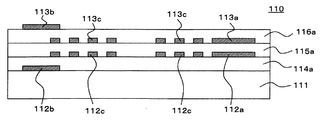
具体的には、特許文献1には、図15に示すように、絶縁体層115aを介して厚み方向で互いに対向するように形成された一対のコイル導体112(112a,112c),113(113a,113c)を一方の磁性体板111の上に薄膜で形成し、さらに他方の磁性体板(図示省略)を貼り付けたコモンモードチョークコイル110が記載されている。
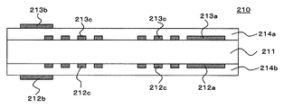
また、特許文献2には、図16に示すように、例えばガラス・エポキシ樹脂基板211の上面及び下面に導体パターン212(212a,212c)、213(213a,213c)がそれぞれ形成された積層型コモンモードチョークコイル210が従来技術として記載されている。
Specifically, in Patent Document 1, as shown in FIG. 15, a pair of coil conductors 112 (112a, 112c), 113 (113a) formed so as to face each other in the thickness direction via an
Further, in Patent Document 2, as shown in FIG. 16, for example, a laminated common in which conductor patterns 212 (212a, 212c) and 213 (213a, 213c) are formed on the upper and lower surfaces of a glass /
しかしながら、上記前者の背景技術に記載のコモンモードチョークコイル110においては、一方の磁性体板111上に一対のコイル導体112、113を薄膜で形成するので、加工プロセス等のハンドリング時に磁性体基板111にカケやワレが生じやすいという課題があった。 また、上記後者の背景技術に記載のコモンモードチョークコイル210においては、エッチング等の加工プロセスのハンドリング性を考慮すると、ガラス・エポキシ樹脂基板211の厚みを小さくすることが難しい。このため、一対のコイル導体212,213間の距離が離れ、コモンモードチョークコイル210として特性(結合度)を高くすることが難しいという課題があった。
However, in the common
本発明は、以上のような事情に鑑みてなされたものであって、一対のコイル導体間の距離を小さくしても安定生産可能なコモンモードチョークコイル用内層基板を提供することを目的とする。また、本発明は、コモンモードチョークコイル用内層基板を用いて容易に生産することができるコモンモードチョークコイルを提供することを目的とする。また、本発明は、前記コモンモードチョークコイル用内層基板を安定して得ることが可能な製造方法を提供することを目的とする。 The present invention has been made in view of the above circumstances, and an object thereof is to provide an inner substrate for a common mode choke coil that can be stably produced even if the distance between a pair of coil conductors is reduced. . Another object of the present invention is to provide a common mode choke coil that can be easily produced using an inner layer substrate for a common mode choke coil. Another object of the present invention is to provide a manufacturing method capable of stably obtaining the inner layer substrate for a common mode choke coil.
本発明のコモンモードチョークコイル用内層基板は、
(1)非磁性で絶縁性の基板と、
該基板の一方の主面上に形成された第1のコイル導体および該コイル導体の一端に接続された一方の引出電極と、
前記基板の他方の主面上に形成され該基板を貫通するスルーホール導体により前記第1のコイル導体の他端と接続されて前記第1のコイル導体及び前記一方の引出電極とともに第1のコイルを構成する他方の引出電極と、
前記第1のコイルを被覆するように前記基板の両主面にそれぞれ形成された第1の絶縁体層と、
前記基板の一方の主面側の第1の絶縁体層上に前記第1のコイル導体および一方の引出電極に対向するように形成された第2のコイル導体および該コイル導体の一端に接続された一方の引出電極と、
前記第2のコイル導体および一方の引出電極を被覆するように形成された第2の絶縁体層と、
前記第2の絶縁体層上に形成され前記第2のコイル導体の他端に前記第2の絶縁体層を貫通するビアホール導体により接続されて前記第2のコイル導体及び前記一方の引出電極とともに第2のコイルを構成する他方の引出電極と、
を備える。(以下、第1の課題解決手段と称する。)
The inner layer substrate for the common mode choke coil of the present invention is
(1) a non-magnetic insulating substrate;
A first coil conductor formed on one main surface of the substrate and one extraction electrode connected to one end of the coil conductor;
A first coil together with the first coil conductor and the one extraction electrode is connected to the other end of the first coil conductor by a through-hole conductor formed on the other main surface of the substrate and penetrating the substrate. The other extraction electrode constituting
A first insulator layer formed on each main surface of the substrate so as to cover the first coil;
A second coil conductor formed on the first insulator layer on one main surface side of the substrate so as to face the first coil conductor and the one extraction electrode, and one end of the coil conductor are connected. One extraction electrode,
A second insulator layer formed to cover the second coil conductor and one extraction electrode;
Along with the second coil conductor and the one extraction electrode, the second coil conductor is formed on the second insulator layer and connected to the other end of the second coil conductor by a via-hole conductor penetrating the second insulator layer. The other extraction electrode constituting the second coil;
Is provided. (Hereinafter referred to as first problem solving means.)
上記コモンモードチョークコイル用内層基板の主要な形態の一つは、(2)前記第1のコイルを被覆する第1の絶縁体層が、前記基板の両主面にそれぞれプリプレグを積層した後、熱プレスすることにより同時に形成されたものである。(以下、第2の課題解決手段と称する。) One of the main forms of the inner layer substrate for the common mode choke coil is: (2) after the first insulator layer covering the first coil is laminated with prepregs on both main surfaces of the substrate, It was formed at the same time by hot pressing. (Hereinafter referred to as the second problem solving means.)
また、本発明のコモンモードチョークコイルは、
(3)上記第1の課題解決手段に記載の内層基板の両主面にそれぞれ磁性体基板が貼着されるとともに、
前記内層基板の端面に露出する前記引き出し電極に接続するように前記基板の端面及びその近傍に端子電極が形成されている。(以下、第3の課題解決手段と称する。)
The common mode choke coil of the present invention is
(3) A magnetic substrate is attached to both main surfaces of the inner layer substrate described in the first problem solving means, respectively,
Terminal electrodes are formed on and near the end surface of the substrate so as to be connected to the lead electrode exposed on the end surface of the inner layer substrate. (Hereinafter referred to as third problem solving means.)
また、本発明のコモンモードチョークコイル用内層基板の製造方法は、
(4)非磁性で絶縁性の基板の一方の主面上に、第1のコイル導体および該コイル導体の一端に接続される一方の引出電極を形成するとともに、
前記基板の他方の主面上に、該基板を貫通するスルーホール導体により前記第1のコイル導体の他端と接続される他方の引出電極を形成して、第1のコイルを準備するステップと、
前記基板の両主面にそれぞれ前記第1のコイルを被覆するように第1の絶縁体層を形成するステップと、
前記基板の一方の主面側の前記第1の絶縁体層上に前記第1のコイル導体および該コイル導体の一端に接続された一方の引出電極と対向するように第2のコイル導体および該コイル導体の一端に接続される一方の引出電極を形成するステップと、
前記基板の一方の主面側の前記第2のコイル導体および該コイル導体に接続された一方の引出電極を被覆するように第2の絶縁体層を形成するステップと、
第2の絶縁体層に前記第2のコイル導体の他方の端部を露出するように下孔を形成するステップと、
第2の絶縁体層上に前記下孔から露出された前記第2のコイル導体の他方の端部に接続するように他方の引出電極を形成するステップと、
を備える。(以下、第4の課題解決手段と称する。)
In addition, the method of manufacturing the inner layer substrate for a common mode choke coil according to the present invention includes:
(4) forming a first coil conductor and one lead electrode connected to one end of the coil conductor on one main surface of the non-magnetic and insulating substrate;
Forming the other lead electrode connected to the other end of the first coil conductor by a through-hole conductor penetrating the substrate on the other main surface of the substrate to prepare a first coil; ,
Forming a first insulator layer on both main surfaces of the substrate so as to cover the first coil, respectively;
The second coil conductor and the second coil conductor on the first insulator layer on one main surface side of the substrate so as to face the first coil conductor and one lead electrode connected to one end of the coil conductor, Forming one extraction electrode connected to one end of the coil conductor;
Forming a second insulator layer so as to cover the second coil conductor on one main surface side of the substrate and one lead electrode connected to the coil conductor;
Forming a pilot hole in the second insulator layer so as to expose the other end of the second coil conductor;
Forming the other lead electrode on the second insulator layer to connect to the other end of the second coil conductor exposed from the pilot hole;
Is provided. (Hereinafter referred to as the fourth problem solving means.)
また、上記コモンモードチョークコイル用内層基板の製造方法の主要な形態の一つは、(5)前記基板の一方の主面側の前記第2の絶縁体層を形成するステップにおいて、同時に、前記基板の他方の主面側の前記第1の絶縁体層上に第2の絶縁体層を形成する。(以下、第5の課題解決手段と称する。) In addition, one of the main forms of the method for manufacturing the inner substrate for the common mode choke coil is (5) in the step of forming the second insulator layer on the one main surface side of the substrate, A second insulator layer is formed on the first insulator layer on the other main surface side of the substrate. (Hereinafter, referred to as fifth problem solving means.)
上記第1の課題解決手段による作用は次の通りである。すなわち、絶縁性の基板の両主面に第1のコイルが分割形成されるとともに、第1のコイルと対向する第2のコイルが、前記基板の両主面にそれぞれ形成された絶縁体層のうちの一方の上に形成されている。このため、第1のコイルと第2のコイルとの間に配置される絶縁体層の厚みを小さくできるとともに、前記第1のコイルを被覆する絶縁体層を形成する際の反りの発生が防止される。 The operation of the first problem solving means is as follows. That is, the first coil is divided and formed on both main surfaces of the insulating substrate, and the second coil facing the first coil is formed of the insulator layer formed on both main surfaces of the substrate. Formed on one of them. For this reason, while being able to make the thickness of the insulator layer arrange | positioned between a 1st coil and a 2nd coil small, generation | occurrence | production of the curvature at the time of forming the insulator layer which coat | covers the said 1st coil is prevented. Is done.
上記第2の課題解決手段による作用は次の通りである。すなわち、前記第1のコイルを被覆する第1の絶縁体層が、前記基板の両主面にそれぞれプリプレグを積層した後、熱プレスすることにより同時に形成されたものである。このため、該絶縁体層を形成する際の硬化時の収縮応力が基板の両主面でバランスされて、反りの発生が抑制される。 The operation of the second problem solving means is as follows. That is, the first insulator layer covering the first coil is formed simultaneously by laminating prepregs on both main surfaces of the substrate and then hot pressing. For this reason, the shrinkage stress at the time of curing when forming the insulator layer is balanced on both main surfaces of the substrate, and the occurrence of warpage is suppressed.
また、上記第3の課題解決手段による作用は次の通りである。すなわち、前記第1の課題解決手段に記載の内層基板の両主面にそれぞれ磁性体基板が貼着されるので、基板のカケやワレの発生が防止される。 The operation of the third problem solving means is as follows. That is, since the magnetic substrate is adhered to both main surfaces of the inner layer substrate described in the first problem solving means, the occurrence of chipping or cracking of the substrate is prevented.
また、上記第4の課題解決手段による作用は次の通りである。すなわち、非磁性で絶縁性の基板の一方の主面上に、第1のコイル導体および該コイル導体の一端に接続される一方の引出電極を、また、前記基板の他方の主面上に、該基板を貫通するスルーホール導体により前記第1のコイル導体の他端と接続される他方の引出電極を、それぞれ分割形成して、第1のコイルを準備するステップと、
前記基板の両主面にそれぞれ前記第1のコイルを被覆するように第1の絶縁体層を形成するステップと、
前記基板の一方の主面側の前記第1の絶縁体層上に前記第1のコイル導体および該コイル導体の一端に接続された一方の引出電極と対向するように第2のコイル導体および該コイル導体の一端に接続される一方の引出電極を形成するステップと、を有する。このため、前記第1のコイルと前記第2のコイルとの間に位置する絶縁体層を薄く形成できるとともに、該絶縁体層を形成する際に前記基板の他方の主面側にも同時に絶縁体層が形成されるので、硬化時の収縮応力が基板の両主面でバランスされて、反りの発生が抑制される。
The operation of the fourth problem solving means is as follows. That is, on one main surface of the non-magnetic and insulating substrate, the first coil conductor and one extraction electrode connected to one end of the coil conductor, and on the other main surface of the substrate, Providing the first coil by separately forming the other extraction electrode connected to the other end of the first coil conductor by a through-hole conductor penetrating the substrate;
Forming a first insulator layer on both main surfaces of the substrate so as to cover the first coil, respectively;
The second coil conductor and the second coil conductor on the first insulator layer on one main surface side of the substrate so as to face the first coil conductor and one lead electrode connected to one end of the coil conductor, Forming one extraction electrode connected to one end of the coil conductor. For this reason, the insulator layer located between the first coil and the second coil can be formed thin, and the other main surface side of the substrate is also insulated at the same time when the insulator layer is formed. Since the body layer is formed, the shrinkage stress at the time of curing is balanced on both main surfaces of the substrate, and the occurrence of warpage is suppressed.
また、上記第5の課題解決手段による作用は次の通りである。すなわち、記基板の一方の主面側の前記第2の絶縁体層を形成するステップにおいて、同時に、前記基板の他方の主面側の前記第1の絶縁体層上に第2の絶縁体層を形成するので、前記第2の絶縁体層の厚みを増加させても、硬化時の収縮応力が基板の両主面でバランスされて、反りの発生が抑制される。 The operation of the fifth problem solving means is as follows. That is, in the step of forming the second insulator layer on one main surface side of the substrate, a second insulator layer is simultaneously formed on the first insulator layer on the other main surface side of the substrate. Therefore, even if the thickness of the second insulator layer is increased, the shrinkage stress at the time of curing is balanced on both main surfaces of the substrate, and the occurrence of warpage is suppressed.
本発明のコモンモードチョークコイル用内層基板によれば、第1のコイルと第2のコイルとの間に配置される絶縁体層の厚みを小さくできるとともに、前記第1のコイルを被覆する絶縁体層を形成する際の反りの発生が防止されるので、安定生産可能なコモンモードチョークコイルを提供することができる。 According to the inner layer substrate for a common mode choke coil of the present invention, the thickness of the insulator layer disposed between the first coil and the second coil can be reduced, and the insulator covering the first coil Since the occurrence of warpage when forming the layer is prevented, a common mode choke coil capable of stable production can be provided.
また、本発明のコモンモードチョークコイルによれば、上記内層基板の両主面にそれぞれ磁性体基板が貼着されるので、磁性体基板のカケやワレが発生しにくい安定生産可能なコモンモードチョークコイルを提供することができる。 In addition, according to the common mode choke coil of the present invention, since the magnetic substrate is adhered to both main surfaces of the inner layer substrate, the common mode choke that can be stably produced is free from the occurrence of chipping and cracking of the magnetic substrate. A coil can be provided.
また、本発明のコモンモードチョークコイル用内層基板の製造方法によれば、前記第1のコイルと前記第2のコイルとの間に位置する絶縁体層を薄く形成できるとともに、該絶縁体層を形成する際に前記基板の他方の主面側にも同時に絶縁体層が形成されるので、硬化時の収縮応力が基板の両主面でバランスされて、反りの発生が抑制され、コモンモードチョークコイル用内層基板を安定生産することができる。 In addition, according to the method for manufacturing an inner layer substrate for a common mode choke coil of the present invention, an insulator layer positioned between the first coil and the second coil can be formed thin, and the insulator layer is Since the insulator layer is also formed on the other main surface side of the substrate at the same time, the shrinkage stress at the time of curing is balanced on both main surfaces of the substrate, so that the occurrence of warpage is suppressed and the common mode choke is suppressed. The coil inner layer substrate can be stably produced.
また、本発明のコモンモードチョークコイル用内層基板の製造方法によれば、前記第2の絶縁体層の厚みを増加させても、硬化時の収縮応力が基板の両主面でバランスされて、反りの発生が抑制され、コモンモードチョークコイル用内層基板を安定生産することができる。
本発明の上記目的とそれ以外の目的、構成特徴、作用効果は、以下の説明と添付図面によって明らかとなろう。
Further, according to the method for manufacturing an inner layer substrate for a common mode choke coil of the present invention, even if the thickness of the second insulator layer is increased, shrinkage stress during curing is balanced on both main surfaces of the substrate, The occurrence of warpage is suppressed, and the inner substrate for the common mode choke coil can be stably produced.
The above object and other objects, structural features, and operational effects of the present invention will become apparent from the following description and the accompanying drawings.
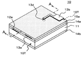
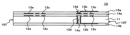
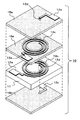
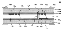
まず、図1〜図3を用いて本発明のコモンモードチョークコイル用内層基板の第1の実施形態について説明する。図1は本実施形態のコモンモードチョークコイル用内層基板10の全体構造を示す外観斜視図である。図2は、本実施形態のコモンモードチョークコイル用内層基板10の内部構造を示す前記図1のA−A線における縦断面図である。図3は、本実施形態のコモンモードチョークコイル用内層基板10の内部構造を示す分解斜視図である。図中、11は絶縁性の基板、12(12a,12b,12c,12d)は第1のコイル、13(13a,13b,13c,13d)は第2のコイル、14(14a,14b)は第1の絶縁体層、15aは第2の絶縁体層である。
First, a first embodiment of an inner layer substrate for a common mode choke coil according to the present invention will be described with reference to FIGS. FIG. 1 is an external perspective view showing the entire structure of the common mode choke coil
本実施形態のコモンモードチョークコイル用内層基板10は、
非磁性で絶縁性の基板11と、
該基板11の一方の主面上に形成された第1のコイル導体12cおよび該コイル導体12cの一端に接続された一方の引出電極12aと、
前記基板11の他方の主面上に形成され該基板11を貫通するスルーホール導体12dにより前記第1のコイル導体12cの他端と接続されて前記第1のコイル導体12c及び前記一方の引出電極12aとともに第1のコイル12を構成する他方の引出電極12bと、前記第1のコイル12を被覆するように前記基板11の両主面にそれぞれ形成された第1の絶縁体層14a,14bと、
前記基板11の一方の主面側の第1の絶縁体層14a上に前記第1のコイル導体12cおよび一方の引出電極12aに対向するように形成された第2のコイル導体13cおよび該コイル導体13cの一端に接続された一方の引出電極13aと、
前記第2のコイル導体13cおよび一方の引出電極13aを被覆するように形成された第2の絶縁体層15aと、
前記第2の絶縁体層15a上に形成され前記第2のコイル導体13cの他端に前記第2の絶縁体層15aを貫通するビアホール導体13dにより接続されて前記第2のコイル導体13c及び前記一方の引出電極13aとともに第2のコイル13を構成する他方の引出電極13bと、を備える。
The
A non-magnetic insulating
A
The
A
A
The
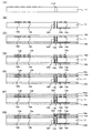
次に、本発明のコモンモードチョークコイル用内層基板の製造方法の第1の実施形態について、図4を参照して説明する。図4(A)〜図4(G)は、本実施形態のコモンモードチョークコイル用内層基板の製造方法をプロセスを追って説明するための縦断面図である。
本実施形態のコモンモードチョークコイル用内層基板の製造方法は、
まず、図4(A)に示すように非磁性で絶縁性の基板11を用意し、次に、図4(B)に示すように該基板11の一方の主面上に、第1のコイル導体12cおよび該コイル導体12cの一端に接続される一方の引出電極12aを、また、前記基板11の他方の主面上に、該基板11を貫通するスルーホール導体12dにより前記第1のコイル導体12cの他端と接続される他方の引出電極12bを、それぞれ分割して形成して、第1のコイル12を準備する。
次に、図4(C)に示すように、前記基板11の両主面にそれぞれ前記第1のコイル12を被覆するように第1の絶縁体層14a,14bを形成する。
次に、図4(D)に示すように、前記基板11の一方の主面側の前記第1の絶縁体層14a上に前記第1のコイル導体12cおよび該コイル導体12cの一端に接続された一方の引出電極12aと対向するように第2のコイル導体13cおよび該コイル導体13cの一端に接続される一方の引出電極13aを形成する。
次に、図4(E)に示すように、前記基板11の一方の主面側の前記第2のコイル導体13cおよび該コイル導体13cに接続された一方の引出電極13aを被覆するように第2の絶縁体層15aを形成する。
次に、図4(F)に示すように、第2の絶縁体層15aに前記第2のコイル導体13cの他方の端部を露出するように下孔15dを形成する。
次に、図4(G)に示すように、第2の絶縁体層15a上に前記下孔15dから露出された前記第2のコイル導体13cの他方の端部に接続するように他方の引出電極13bを形成する。こうして、図2に示す前記第1の実施形態のコモンモードチョークコイル用内層基板10が得られる。
Next, a first embodiment of a method for manufacturing an inner layer substrate for a common mode choke coil according to the present invention will be described with reference to FIG. 4 (A) to 4 (G) are longitudinal sectional views for explaining the manufacturing method of the common mode choke coil inner layer substrate according to the present embodiment step by step.
The manufacturing method of the inner layer substrate for the common mode choke coil of the present embodiment is as follows:
First, a nonmagnetic insulating
Next, as shown in FIG. 4C, first insulator layers 14a and 14b are formed on both main surfaces of the
Next, as shown in FIG. 4D, the
Next, as shown in FIG. 4E, the
Next, as shown in FIG. 4F, a
Next, as shown in FIG. 4 (G), the other lead is connected to the other end of the
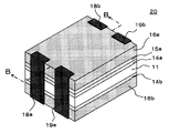
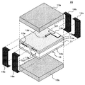
次に、前記内層基板10を用いた本発明のコモンモードチョークコイルの第1の実施形態について、図5〜図7を参照して説明する。図5は本実施形態のコモンモードチョークコイル20の全体構造を示す外観斜視図である。図6は本実施形態のコモンモードチョークコイル20の前記図5のB−B線における縦断面図である。また、図7は、本実施形態のコモンモードチョークコイル20の内部構造を示す分解斜視図である。
Next, a first embodiment of the common mode choke coil of the present invention using the
本実施形態のコモンモードチョークコイル20は、前記第1の実施形態のコモンモードチョークコイル用内層基板10の両主面にそれぞれ磁性体基板16a,16bが貼着されるとともに、前記内層基板10の端面10Tに露出する前記引出電極12a,12b,13a,13bに接続するように前記基板10の端面及びその近傍に端子電極18a,18b,19a,19bが形成されている。
In the common
次に、本発明のコモンモードチョークコイル用内層基板10の各部の好ましい実施形態について、説明する。
Next, a preferred embodiment of each part of the common mode choke coil
先ず、上記非磁性で絶縁性の基板11の好ましい実施形態は次の通りである。すなわち、上記基板11の材料としては、例えば、エポキシ系の未硬化樹脂をガラス繊維布に含浸させたもの(FR−4、FR−5)や、ガラス繊維布にさらにガラス不織布を複合使用したもの(CEM−3)等、所謂プリプレグと呼ばれるBステージ基板から選択して用いることが好ましい。前記基板11の厚みは、例えば40〜60μmであることが好ましい。また、前記基板11は、複数のコモンモードチョークコイルを一括して作成するために、例えば長さ50〜120mm、幅50〜120mmであることが好ましい。また、該基板11を貫通するスルーホール導体を形成するために、前記基板11に予めドリル加工やレーザ光照射等により下孔11を形成しておくことが好ましい。
First, a preferred embodiment of the nonmagnetic insulating
次に、上記コイル導体12c、13c、及び引出電極12a,12b,13a,13bの好ましい実施形態は次の通りである。すなわち、上記コイル導体12c,13c、及び引出電極12a,12b,13a,13bの材料としては、例えば銅が好ましい。前記コイル導体12c、13cおよび引出電極12a,12b,13a,13bの厚みは、例えば5〜20μmであることが好ましい。また、前記コイル導体12c、13cの線幅は例えば10〜30μmであることが好ましい。上記コイル導体12c、13c及び引出電極12a,12b,13a,13bの形成方法は、例えばシード層上に銅メッキすることにより形成することが好ましい。また、銅箔にエッチングすることにより形成してもよい。
Next, preferred embodiments of the
次に、上記スルーホール導体12dの好ましい実施形態は次の通りである。すなわち、上記スルーホール導体12dの材料としては、銅が好ましい。前記スルーホール導体12dの厚みは、例えば5〜10μmであることが好ましい。また、前記スルーホール導体12dの直径は例えば30〜100μmであることが好ましい。上記スルーホール導体12dの形成方法は、例えば銅を化学めっきすることにより形成することが好ましい。また、銅メッキ膜上にさらに銅を電解メッキすることが好ましい。
Next, a preferred embodiment of the through-
次に、上記ビアホール導体13dの好ましい実施形態は次の通りである。すなわち、上記ビアホール導体13dの材料としては、例えば銅が好ましい。前記ビアホール導体13dの厚みは、例えば5〜10μmであることが好ましい。また、前記ビアホール導体13dの直径は例えば30〜100μmであることが好ましい。上記ビアホール導体13dの形成方法は、例えば銅を化学メッキすることにより形成することが好ましい。また、銅メッキ膜上にさらに銅を電解メッキすることが好ましい。
Next, a preferred embodiment of the via-
次に、上記第1の絶縁体層14a,14b及び第2の絶縁体層15aの好ましい実施形態は次の通りである。すなわち、上記第1の絶縁体層14a,14b及び第2の絶縁体層15aの材料としては、FR−4のようにエポキシ系の未硬化樹脂をガラス繊維布に含浸させた所謂プリプレグと呼ばれるBステージ基板から選択して用いることが好ましい。前記第1の絶縁体層14a,14b及び第2の絶縁体層15aの厚みは、例えば10〜40μmであることが好ましい。また、前記第1の絶縁体層14a,14b及び第2の絶縁体層15aの形成方法は、例えば上記基板11の主面上に上記プリプレグを積層し熱プレスすることにより形成することが好ましい。
Next, preferred embodiments of the first insulator layers 14a and 14b and the
次に、上記磁性体基板16a,16bの好ましい実施形態は次の通りである。すなわち、上記磁性体基板16a,16bの材料としては、例えばフェライト磁性粉や金属磁性粉と樹脂とを混合してなる複合磁性体シートや焼結フェライト板等から選択して用いることが好ましい。前記磁性体基板16a,16bの厚みは、例えば200〜400μmであることが好ましい。また、前記コモンモードチョークコイル用内層基板10の両主面への上記磁性体基板16a,16bの貼着は、例えばエポキシ樹脂やポリフェニレンエーテル(PPE)等を主成分とする接着シートや接着剤を接着手段として用い、例えば180℃で熱プレス等の熱処理を施すことにより貼着することができる。
Next, a preferred embodiment of the
次に、上記端子電極18a,18b,19a,19bの好ましい実施形態は次の通りである。すなわち、上記端子電極18a,18b,19a,19bの材料としては、銀、銅、ニッケル等から選択された金属、または前記金属の粒子を樹脂中に含有させた導電性樹脂を用いることが好ましい。前記端子電極18a,18b,19a,19bの厚みは、例えば20〜80μmであることが好ましい。また、前記端子電極18a,18b,19a,19bの形成方法は、例えば前記金属の粉末と樹脂とを混合して電極材料ペーストとし、これを塗布した後、例えば150℃で熱処理して硬化することが好ましい。また、得られた電極膜上に、さらに、例えばSnメッキ等のはんだ付け性の良好な膜を形成することが好ましい。また、前記電極材料ペーストの塗布・硬化に限定するものではなく、例えば銅をスパッタしてシード層を形成した後、該シード層上に例えば電解メッキにより前記金属からなる電極膜を成長させてもよい。
Next, preferred embodiments of the
(実施例1)
次に、本発明のコモンモードチョークコイル用内層基板の実施例について説明する。
まず、図4(A)に示すようにFR−4からなり、長さ120mm、幅120mm、厚さ60μmの非磁性で絶縁性の基板11を用意した。該基板11には、後にスルーホール導体を形成する位置に予め直径60μmの下孔11dをレーザ光照射により形成した。
次に、図4(B)に示すように該基板11の両主面及び前記下孔11dの内周面に、銅を化学メッキして図示省略したシード層を形成した。次に、該シード層上に感光性樹脂からなる厚さ20μmのフィルムを接着してレジスト膜を形成した。次に所定のマスクを用いて露光し、不要なレジスト膜を除去した後、銅を電解メッキして、厚さ10μmの第1のコイル導体12cおよび該コイル導体12cの一端に接続される一方の引出電極12aを、また、前記基板11の他方の主面上に、該基板11を貫通するスルーホール導体12dにより前記第1のコイル導体12cの他端と接続される他方の引出電極12bを、それぞれ分割して形成して、第1のコイル12を準備した。
次に、図4(C)に示すように、前記基板11の両主面にそれぞれ前記第1のコイル12を被覆するようにFR−4からなるプリプレグを積層し、180℃で80分間熱プレスして、厚さ20μmの第1の絶縁体層14a,14bを形成した。
次に、図4(D)に示すように、前記基板11の一方の主面側の前記第1の絶縁体層14a上に、前記と同様に銅をメッキして、前記第1のコイル導体12cおよび該コイル導体12cの一端に接続された一方の引出電極12aと対向するように、厚さ10μmの第2のコイル導体13cおよび該コイル導体13cの一端に接続される一方の引出電極13aを形成した。
次に、図4(E)に示すように、前記と同様にプリプレグを積層し熱プレスして、前記基板11の一方の主面側の前記第2のコイル導体13cおよび該コイル導体13cに接続された一方の引出電極13aを被覆するように厚さ20μmの第2の絶縁体層15aを形成した。
次に、図4(F)に示すように、レーザ光を照射して、第2の絶縁体層15aに前記第2のコイル導体13cの他方の端部を露出するように直径60μmの下孔15dを形成した。
次に、図4(G)に示すように、銅をメッキして、第2の絶縁体層15a上に前記下孔15dから露出された前記第2のコイル導体13cの他方の端部に接続するように厚さ10μmの他方の引出電極13bを形成した。こうして、図2に示す前記第1の実施形態のコモンモードチョークコイル用内層基板10を得た。
Example 1
Next, examples of the inner layer substrate for a common mode choke coil of the present invention will be described.
First, as shown in FIG. 4A, a nonmagnetic insulating
Next, as shown in FIG. 4B, a seed layer (not shown) was formed by chemical plating of copper on both main surfaces of the
Next, as shown in FIG. 4C, prepregs made of FR-4 are laminated on both main surfaces of the
Next, as shown in FIG. 4D, the first coil conductor is plated on the
Next, as shown in FIG. 4E, the prepreg is laminated and heat-pressed in the same manner as described above, and connected to the
Next, as shown in FIG. 4 (F), a laser beam is irradiated to prepare a pilot hole having a diameter of 60 μm so that the other end of the
Next, as shown in FIG. 4G, copper is plated and connected to the other end of the
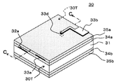
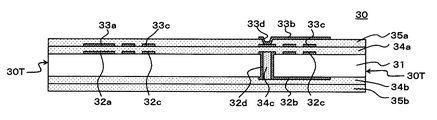
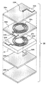
次に、図8〜図10を用いて本発明のコモンモードチョークコイル用内層基板の第2の実施形態について説明する。図8は本実施形態のコモンモードチョークコイル用内層基板30の全体構造を示す外観斜視図である。図9は、本実施形態のコモンモードチョークコイル用内層基板30の内部構造を示す前記図8のC−C線における縦断面図である。図10は、本実施形態のコモンモードチョークコイル用内層基板30の内部構造を示す分解斜視図である。図中、31は絶縁性の基板、32(32a,32b,32c,32d)は第1のコイル、33(33a,33b,33c,33d)は第2のコイル、34a,34bは第1の絶縁体層、35a,35bは第2の絶縁体層である。
Next, a second embodiment of the inner layer substrate for a common mode choke coil according to the present invention will be described with reference to FIGS. FIG. 8 is an external perspective view showing the entire structure of the common mode choke coil
本実施形態のコモンモードチョークコイル用内層基板30は、
非磁性で絶縁性の基板31と、
該基板31の一方の主面上に形成された第1のコイル導体32cおよび該コイル導体32cの一端に接続された一方の引出電極32aと、
前記基板31の他方の主面上に形成され該基板31を貫通するスルーホール導体32dにより前記第1のコイル導体32cの他端と接続されて前記第1のコイル導体32c及び前記一方の引出電極32aとともに第1のコイル32を構成する他方の引出電極32bと、前記第1のコイル32を被覆するように前記基板31の両主面にそれぞれ形成された第1の絶縁体層34a,34bと、
前記基板31の一方の主面側の第1の絶縁体層34a上に前記第1のコイル導体32cおよび一方の引出電極32aに対向するように形成された第2のコイル導体33cおよび該コイル導体33cの一端に接続された一方の引出電極33aと、
前記基板31の一方の主面側の前記第2のコイル導体33cおよび一方の引出電極33aを被覆するように、また前記基板31の他方の主面側の前記第1の絶縁体層34bを被覆するように、それぞれ形成された第2の絶縁体層35a、35bと、
前記基板31の一方の主面側の第2の絶縁体層35a上に形成され前記第2のコイル導体33cの他端に前記第2の絶縁体層35aを貫通するビアホール導体33dにより接続されて前記第2のコイル導体33c及び前記一方の引出電極33aとともに第2のコイル33を構成する他方の引出電極33bと、を備える。
The
A non-magnetic insulating
A
The
A
Covering the
A via-
次に、本発明のコモンモードチョークコイル用内層基板の製造方法の第2の実施形態について、図11を参照して説明する。図11(A)〜図11(G)は、本実施形態のコモンモードチョークコイル用内層基板の製造方法をプロセスを追って説明するための縦断面図である。
本実施形態のコモンモードチョークコイル用内層基板の製造方法は、
まず、図11(A)に示すように非磁性で絶縁性の基板31を用意し、次に、図11(B)に示すように該基板31の一方の主面上に、第1のコイル導体32cおよび該コイル導体32cの一端に接続される一方の引出電極32aを、また、前記基板31の他方の主面上に、該基板31を貫通するスルーホール導体32dにより前記第1のコイル導体32cの他端と接続される他方の引出電極32bを、それぞれ分割して形成して、第1のコイル32を準備する。
次に、図11(C)に示すように、前記基板31の両主面にそれぞれ前記第1のコイル32を被覆するように第1の絶縁体層34a,34bを形成する。
次に、図11(D)に示すように、前記基板31の一方の主面側の前記第1の絶縁体層34a上に前記第1のコイル導体32cおよび該コイル導体32cの一端に接続された一方の引出電極32aと対向するように第2のコイル導体33cおよび該コイル導体33cの一端に接続される一方の引出電極33aを形成する。
次に、図11(E)に示すように、前記基板31の一方の主面側の前記第2のコイル導体33cおよび該コイル導体33cに接続された一方の引出電極33aを被覆するように、また、前記基板32の他方の主面側の前記第1の絶縁体層34bを被覆するように、それぞれ第2の絶縁体層35a、35bを形成する。
次に、図11(F)に示すように、第2の絶縁体層35aに前記第2のコイル導体33cの他方の端部を露出するように下孔35dを形成する。
次に、図11(G)に示すように、第2の絶縁体層35a上に前記下孔35dから露出された前記第2のコイル導体33cの他方の端部に接続するように他方の引出電極33bを形成する。こうして、図9に示す前記第2の実施形態のコモンモードチョークコイル用内層基板30が得られる。
Next, a second embodiment of the method for manufacturing an inner layer substrate for a common mode choke coil according to the present invention will be described with reference to FIG. FIG. 11A to FIG. 11G are longitudinal cross-sectional views for explaining the manufacturing method of the common mode choke coil inner layer substrate according to the present embodiment step by step.
The manufacturing method of the inner layer substrate for the common mode choke coil of the present embodiment is as follows:
First, as shown in FIG. 11A, a non-magnetic and insulating
Next, as shown in FIG. 11C, first insulator layers 34a and 34b are formed on both main surfaces of the
Next, as shown in FIG. 11D, the
Next, as shown in FIG. 11E, the
Next, as shown in FIG. 11F, a
Next, as shown in FIG. 11 (G), the other lead is connected to the other end of the
本実施形態のコモンモードチョークコイル用内層基板30が先の第1の実施形態のコモンモードチョークコイル用内層基板10と異なるところは、前記基板31の他方の主面側の第1の絶縁体層34b上に該第1の絶縁体層34bを覆うように第2の絶縁体層35bが形成されている点にある。これによれば、前記第2の絶縁体層35aの厚みが厚い場合であっても、反りの発生を抑制することができる。その他の構成及び作用効果は先の第1の実施形態のコモンモードチョークコイル用内層基板10と同様であるため、説明を省略する。
The common mode choke coil
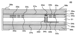
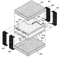
次に、前記内層基板30を用いた本発明のコモンモードチョークコイルの第2の実施形態について、図12〜図14参照して説明する。図12は本実施形態のコモンモードチョークコイル40の全体構造を示す外観斜視図である。図13は本実施形態のコモンモードチョークコイル40の前記図12のD−D線における縦断面図である。また、図14は、本実施形態のコモンモードチョークコイル40の内部構造を示す分解斜視図である。
Next, a second embodiment of the common mode choke coil of the present invention using the
本実施形態のコモンモードチョークコイル40は、前記第2の実施形態のコモンモードチョークコイル用内層基板30の両主面にそれぞれ磁性体基板36a,36bが貼着されるとともに、前記内層基板30の端面30Tに露出する前記引出電極32a,32b,33a,33bに接続するように前記基板30の端面及びその近傍に端子電極38a,38b,39a,39bが形成されている。
In the common
(実施例2)
次に、本発明のコモンモードチョークコイル用内層基板の実施例について説明する。
まず、図11(A)に示すようにFR−4からなり、長さ120mm、幅120mm、厚さ60μmの非磁性で絶縁性の基板31を用意した。該基板31には、後にスルーホール導体を形成する位置に予め直径60μmの下孔31dをレーザ光を照射することにより形成した。
次に、図11(B)に示すように該基板31の両主面及び前記下孔31dの内周面に、銅を化学メッキして図示省略したシード層を形成した。次に、該シード層上に感光性樹脂からなる厚さ20μmのフィルムを接着してレジスト膜を形成した。次に所定のマスクを用いて露光し不要なレジスト膜を除去した後、銅を電解メッキして、厚さ10μmの第1のコイル導体32cおよび該コイル導体32cの一端に接続される一方の引出電極32aを、また、前記基板31の他方の主面上に、該基板31を貫通するスルーホール導体32dにより前記第1のコイル導体32cの他端と接続される他方の引出電極32bを、それぞれ分割して形成して、第1のコイル32を準備した。
次に、図11(C)に示すように、前記基板31の両主面にそれぞれ前記第1のコイル32を被覆するようにFR−4からなるプリプレグを積層し、180℃で80分間熱プレスして、厚さ20μmの第1の絶縁体層34a,34bを形成した。
次に、図11(D)に示すように、前記基板31の一方の主面側の前記第1の絶縁体層34a上に、前記と同様に銅をメッキして、前記第1のコイル導体32cおよび該コイル導体32cの一端に接続された一方の引出電極32aと対向するように、厚さ10μmの第2のコイル導体33cおよび該コイル導体33cの一端に接続される一方の引出電極33aを形成した。
次に、図11(E)に示すように、前記と同様にプリプレグを積層して、前記基板31の一方の主面側の前記第2のコイル導体33cおよび該コイル導体33cに接続された一方の引出電極33aを被覆するように、また、前記基板31の他方の主面側の前記第1の絶縁体層34bを被覆するように、それぞれ厚さ20μmの第2の絶縁体層35a、35bを形成した。
次に、図11(F)に示すように、レーザ光を照射して、第2の絶縁体層35aに前記第2のコイル導体33cの他方の端部を露出するように直径60μmの下孔35dを形成した。
次に、図11(G)に示すように、銅をメッキして、第2の絶縁体層35a上に前記下孔35dから露出された前記第2のコイル導体33cの他方の端部に接続するように厚さ10μmの他方の引出電極33bを形成した。こうして、図9に示す前記第2の実施形態のコモンモードチョークコイル用内層基板30を得た。
(Example 2)
Next, examples of the inner layer substrate for a common mode choke coil of the present invention will be described.
First, as shown in FIG. 11A, a nonmagnetic insulating
Next, as shown in FIG. 11B, a seed layer (not shown) was formed by chemical plating of copper on both main surfaces of the
Next, as shown in FIG. 11C, prepregs made of FR-4 are laminated on both main surfaces of the
Next, as shown in FIG. 11D, the first coil conductor is plated on the
Next, as shown in FIG. 11 (E), the prepreg is laminated in the same manner as described above, and the
Next, as shown in FIG. 11F, a pilot hole having a diameter of 60 μm is irradiated so as to expose the other end portion of the
Next, as shown in FIG. 11G, copper is plated and connected to the other end of the
10:コモンモードチョークコイル用内層基板。
10T:内層基板の端面
11:基板
11d:下孔
12:第1のコイル
12a:引出電極
12b:引出電極
12c:コイル導体
12d:スルーホール導体
13:第2のコイル
13a:引出電極
13b:引出電極
13c:コイル導体
13d:ビアホール導体
14,14a,14b:第1の絶縁体層
14c:絶縁体
15,15a:第2の絶縁体層
15d:下孔
16a,16b:磁性体基板
17a,17b:接着剤層
18a、18b、19a、19b:端子電極
20:コモンモードチョークコイル
30:コモンモードチョークコイル用内層基板
30T:内層基板の端面
31:基板
31d:下孔
32:第1のコイル
32a:引出電極
32b:引出電極
32c:コイル導体
32d:スルーホール導体
33:第2のコイル
33a:引出電極
33b:引出電極
33c:コイル導体
33d:ビアホール導体
34,34a,34b:第1の絶縁体層
35,35a,35b:第2の絶縁体層
35d:下孔
36a,36b:磁性体基板
37a,37b:接着剤層
38a、38b、39a、39b:端子電極
40:コモンモードチョークコイル
10: Inner layer substrate for common mode choke coil.
10T: end face of inner layer substrate 11:
Claims (5)
該基板の一方の主面上に形成された第1のコイル導体および該コイル導体の一端に接続された一方の引出電極と、
前記基板の他方の主面上に形成され該基板を貫通するスルーホール導体により前記第1のコイル導体の他端と接続されて前記第1のコイル導体及び前記一方の引出電極とともに第1のコイルを構成する他方の引出電極と、
前記第1のコイルを被覆するように前記基板の両主面にそれぞれ形成された第1の絶縁体層と、
前記基板の一方の主面側の第1の絶縁体層上に前記第1のコイル導体および一方の引出電極に対向するように形成された第2のコイル導体および該コイル導体の一端に接続された一方の引出電極と、
前記第2のコイル導体および一方の引出電極を被覆するように形成された第2の絶縁体層と、
前記第2の絶縁体層上に形成され前記第2のコイル導体の他端に前記第2の絶縁体層を貫通するビアホール導体により接続されて前記第2のコイル導体及び前記一方の引出電極とともに第2のコイルを構成する他方の引出電極と、
を備えたことを特徴とするコモンモードチョークコイル用内層基板。 A non-magnetic, insulating substrate;
A first coil conductor formed on one main surface of the substrate and one extraction electrode connected to one end of the coil conductor;
A first coil together with the first coil conductor and the one extraction electrode is connected to the other end of the first coil conductor by a through-hole conductor formed on the other main surface of the substrate and penetrating the substrate. The other extraction electrode constituting
A first insulator layer formed on each main surface of the substrate so as to cover the first coil;
A second coil conductor formed on the first insulator layer on one main surface side of the substrate so as to face the first coil conductor and the one extraction electrode, and one end of the coil conductor are connected. One extraction electrode,
A second insulator layer formed to cover the second coil conductor and one extraction electrode;
Along with the second coil conductor and the one extraction electrode, the second coil conductor is formed on the second insulator layer and connected to the other end of the second coil conductor by a via-hole conductor penetrating the second insulator layer. The other extraction electrode constituting the second coil;
An inner layer substrate for a common mode choke coil, comprising:
前記内層基板の端面に露出する前記引出電極に接続するように前記基板の端面及びその近傍に端子電極が形成された
ことを特徴とするコモンモードチョークコイル。 A magnetic substrate is adhered to both main surfaces of the inner layer substrate according to claim 1, respectively.
A common mode choke coil, wherein a terminal electrode is formed on and near the end surface of the substrate so as to be connected to the extraction electrode exposed on the end surface of the inner layer substrate.
前記基板の他方の主面上に、該基板を貫通するスルーホール導体により前記第1のコイル導体の他端と接続される他方の引出電極を形成して、第1のコイルを準備するステップと、
前記基板の両主面にそれぞれ前記第1のコイルを被覆するように第1の絶縁体層を形成するステップと、
前記基板の一方の主面側の前記第1の絶縁体層上に前記第1のコイル導体および該コイル導体の一端に接続された一方の引出電極と対向するように第2のコイル導体および該コイル導体の一端に接続される一方の引出電極を形成するステップと、
前記基板の一方の主面側の前記第2のコイル導体および該コイル導体に接続された一方の引出電極を被覆するように第2の絶縁体層を形成するステップと、
第2の絶縁体層に前記第2のコイル導体の他方の端部を露出するように下孔を形成するステップと、
第2の絶縁体層上に前記下孔から露出された前記第2のコイル導体の他方の端部に接続するように他方の引出電極を形成するステップと、
を備えたことを特徴とするコモンモードチョークコイル用内層基板の製造方法。 Forming a first coil conductor and one lead electrode connected to one end of the coil conductor on one main surface of the non-magnetic and insulating substrate;
Forming the other lead electrode connected to the other end of the first coil conductor by a through-hole conductor penetrating the substrate on the other main surface of the substrate to prepare a first coil; ,
Forming a first insulator layer on both main surfaces of the substrate so as to cover the first coil, respectively;
The second coil conductor and the second coil conductor on the first insulator layer on one main surface side of the substrate so as to face the first coil conductor and one lead electrode connected to one end of the coil conductor, Forming one extraction electrode connected to one end of the coil conductor;
Forming a second insulator layer so as to cover the second coil conductor on one main surface side of the substrate and one lead electrode connected to the coil conductor;
Forming a pilot hole in the second insulator layer so as to expose the other end of the second coil conductor;
Forming the other lead electrode on the second insulator layer to connect to the other end of the second coil conductor exposed from the pilot hole;
A method for manufacturing an inner layer substrate for a common mode choke coil, comprising:
ことを特徴とする請求項4記載のコモンモードチョークコイル用内層基板の製造方法。 In the step of forming the second insulator layer on one main surface side of the substrate, simultaneously, forming a second insulator layer on the first insulator layer on the other main surface side of the substrate 5. The method for manufacturing an inner layer substrate for a common mode choke coil according to claim 4, wherein:
Priority Applications (1)
| Application Number | Priority Date | Filing Date | Title |
|---|---|---|---|
| JP2008102919A JP2009253233A (en) | 2008-04-10 | 2008-04-10 | Inner-layer substrate for common-mode choke coil, its manufacturing method, and common-mode choke coil |
Applications Claiming Priority (1)
| Application Number | Priority Date | Filing Date | Title |
|---|---|---|---|
| JP2008102919A JP2009253233A (en) | 2008-04-10 | 2008-04-10 | Inner-layer substrate for common-mode choke coil, its manufacturing method, and common-mode choke coil |
Publications (1)
| Publication Number | Publication Date |
|---|---|
| JP2009253233A true JP2009253233A (en) | 2009-10-29 |
Family
ID=41313598
Family Applications (1)
| Application Number | Title | Priority Date | Filing Date |
|---|---|---|---|
| JP2008102919A Withdrawn JP2009253233A (en) | 2008-04-10 | 2008-04-10 | Inner-layer substrate for common-mode choke coil, its manufacturing method, and common-mode choke coil |
Country Status (1)
| Country | Link |
|---|---|
| JP (1) | JP2009253233A (en) |
Cited By (11)
| Publication number | Priority date | Publication date | Assignee | Title |
|---|---|---|---|---|
| JP2012089765A (en) * | 2010-10-21 | 2012-05-10 | Tdk Corp | Coil component |
| CN102479611A (en) * | 2010-11-25 | 2012-05-30 | 乾坤科技股份有限公司 | Inductor and method for manufacturing inductor |
| CN103180919A (en) * | 2010-10-21 | 2013-06-26 | Tdk株式会社 | Coil component and method for producing same |
| JP2014003289A (en) * | 2012-06-14 | 2014-01-09 | Samsung Electro-Mechanics Co Ltd | Manufacturing method of high frequency inductor |
| KR101373540B1 (en) | 2010-05-17 | 2014-03-12 | 다이요 유덴 가부시키가이샤 | Electronic component to be embedded in substrate and component embedded substrate |
| JP2014127717A (en) * | 2012-12-26 | 2014-07-07 | Samsung Electro-Mechanics Co Ltd | Common mode filter and method of manufacturing the same |
| JP2015106704A (en) * | 2013-11-28 | 2015-06-08 | ジョインセット株式会社 | Stack type common mode filter for high frequency |
| JP2015220464A (en) * | 2014-05-19 | 2015-12-07 | サムソン エレクトロ−メカニックス カンパニーリミテッド. | Common mode filter and manufacturing method thereof |
| JP2016167578A (en) * | 2015-03-09 | 2016-09-15 | サムソン エレクトロ−メカニックス カンパニーリミテッド. | Coil electronic component and manufacturing method of same |
| CN108987037A (en) * | 2017-06-05 | 2018-12-11 | 株式会社村田制作所 | The variation of coil component and its frequency characteristic |
| JP2021141499A (en) * | 2020-03-06 | 2021-09-16 | 株式会社豊田中央研究所 | Common mode noise filter |
-
2008
- 2008-04-10 JP JP2008102919A patent/JP2009253233A/en not_active Withdrawn
Cited By (22)
| Publication number | Priority date | Publication date | Assignee | Title |
|---|---|---|---|---|
| KR101373540B1 (en) | 2010-05-17 | 2014-03-12 | 다이요 유덴 가부시키가이샤 | Electronic component to be embedded in substrate and component embedded substrate |
| US9236171B2 (en) | 2010-10-21 | 2016-01-12 | Tdk Corporation | Coil component and method for producing same |
| CN103180919A (en) * | 2010-10-21 | 2013-06-26 | Tdk株式会社 | Coil component and method for producing same |
| KR101434351B1 (en) | 2010-10-21 | 2014-08-26 | 티디케이가부시기가이샤 | Coil component and method for producing same |
| JP2012089765A (en) * | 2010-10-21 | 2012-05-10 | Tdk Corp | Coil component |
| CN103180919B (en) * | 2010-10-21 | 2016-05-18 | Tdk株式会社 | Coil component and manufacture method thereof |
| CN102479611A (en) * | 2010-11-25 | 2012-05-30 | 乾坤科技股份有限公司 | Inductor and method for manufacturing inductor |
| JP2012114444A (en) * | 2010-11-25 | 2012-06-14 | Qiankun Kagi Kofun Yugenkoshi | Method of producing inductor with high inductance |
| TWI641003B (en) * | 2010-11-25 | 2018-11-11 | 乾坤科技股份有限公司 | Inductor |
| CN102479611B (en) * | 2010-11-25 | 2015-04-08 | 乾坤科技股份有限公司 | Inductors and methods of making them |
| JP2014003289A (en) * | 2012-06-14 | 2014-01-09 | Samsung Electro-Mechanics Co Ltd | Manufacturing method of high frequency inductor |
| US9899141B2 (en) | 2012-12-26 | 2018-02-20 | Samsung Electro-Mechanics Co., Ltd. | Common mode filter and method of manufacturing the same |
| JP2014127717A (en) * | 2012-12-26 | 2014-07-07 | Samsung Electro-Mechanics Co Ltd | Common mode filter and method of manufacturing the same |
| JP2015106704A (en) * | 2013-11-28 | 2015-06-08 | ジョインセット株式会社 | Stack type common mode filter for high frequency |
| JP2015220464A (en) * | 2014-05-19 | 2015-12-07 | サムソン エレクトロ−メカニックス カンパニーリミテッド. | Common mode filter and manufacturing method thereof |
| JP2016167578A (en) * | 2015-03-09 | 2016-09-15 | サムソン エレクトロ−メカニックス カンパニーリミテッド. | Coil electronic component and manufacturing method of same |
| KR20160108927A (en) * | 2015-03-09 | 2016-09-21 | 삼성전기주식회사 | Coil electronic component and manufacturing method thereof |
| KR102184566B1 (en) * | 2015-03-09 | 2020-12-02 | 삼성전기주식회사 | Coil electronic component and manufacturing method thereof |
| CN108987037A (en) * | 2017-06-05 | 2018-12-11 | 株式会社村田制作所 | The variation of coil component and its frequency characteristic |
| JP2018206952A (en) * | 2017-06-05 | 2018-12-27 | 株式会社村田製作所 | Coil component and method for changing frequency characteristics thereof |
| US11189416B2 (en) | 2017-06-05 | 2021-11-30 | Murata Manufacturing Co., Ltd. | Coil component and method of changing frequency characteristic thereof |
| JP2021141499A (en) * | 2020-03-06 | 2021-09-16 | 株式会社豊田中央研究所 | Common mode noise filter |
Similar Documents
| Publication | Publication Date | Title |
|---|---|---|
| CN102647854B (en) | Inductor component, printed circuit board incorporating inductor component therein, and method of manufacturing inductor component | |
| TWI233771B (en) | Flexible rigid printed circuit board and method of fabricating the board | |
| JP5614479B2 (en) | Coil parts manufacturing method | |
| US10674608B2 (en) | Printed circuit board and manufacturing method thereof | |
| JP2014032978A (en) | Inductor component, manufacturing method of inductor component, and wiring board | |
| JP5970716B2 (en) | Electronic component and manufacturing method thereof | |
| WO2012053439A1 (en) | Coil component and method for producing same | |
| CN101763933A (en) | Electronic component and manufacturing method of electronic component | |
| JPH08203737A (en) | Coil component | |
| JP2012089765A (en) | Coil component | |
| JP2010080550A (en) | Common mode choke coil | |
| JP5999122B2 (en) | Inductor manufacturing method | |
| US11600430B2 (en) | Inductor including high-rigidity insulating layers | |
| CN103781283A (en) | A method for manufacturing a circuit board | |
| JP2015038908A (en) | Flex-rigid wiring board | |
| JP2013115136A (en) | Substrate with built-in electronic components and manufacturing method of the same | |
| JP4482613B2 (en) | Manufacturing method of multilayer wiring board | |
| JP4330850B2 (en) | Thin coil component manufacturing method, thin coil component, and circuit device using the same | |
| KR102268392B1 (en) | Printed circuit board | |
| KR101987043B1 (en) | Printed circuit board | |
| KR102093155B1 (en) | Printed circuit board | |
| TW201340816A (en) | Flexible-rigid printed circuit board mechanism and method for manufacturing same | |
| CN103299393B (en) | Method of manufacturing printed circuit boards having vias with wrap plating | |
| JPWO2024127588A5 (en) | ||
| JP2024058997A (en) | Multilayer wiring board and its manufacturing method |
Legal Events
| Date | Code | Title | Description |
|---|---|---|---|
| A300 | Withdrawal of application because of no request for examination |
Free format text: JAPANESE INTERMEDIATE CODE: A300 Effective date: 20110705 |