JP2009253000A - Method of manufacturing semiconductor device - Google Patents
Method of manufacturing semiconductor device Download PDFInfo
- Publication number
- JP2009253000A JP2009253000A JP2008098928A JP2008098928A JP2009253000A JP 2009253000 A JP2009253000 A JP 2009253000A JP 2008098928 A JP2008098928 A JP 2008098928A JP 2008098928 A JP2008098928 A JP 2008098928A JP 2009253000 A JP2009253000 A JP 2009253000A
- Authority
- JP
- Japan
- Prior art keywords
- wafer
- electrode film
- manufacturing
- semiconductor device
- based alloy
- Prior art date
- Legal status (The legal status is an assumption and is not a legal conclusion. Google has not performed a legal analysis and makes no representation as to the accuracy of the status listed.)
- Granted
Links
Images


Abstract
Description
本発明は、半導体装置の製造方法に関する。特にMOSゲート側の半導体機能領域の形成、反対側を耐圧に必要な厚さに研削後、不純物拡散層をイオン注入および低温活性化処理により形成する製造方法にかかる絶縁ゲート型バイポーラトランジスタ(IGBT)等の半導体装置の製造方法に関する。 The present invention relates to a method for manufacturing a semiconductor device. In particular, an insulated gate bipolar transistor (IGBT) according to a manufacturing method in which a semiconductor functional region on the MOS gate side is formed and the opposite side is ground to a thickness necessary for withstand voltage, and then an impurity diffusion layer is formed by ion implantation and low-temperature activation processing. The present invention relates to a method for manufacturing a semiconductor device.
従来のIGBTの製造方法について、図2に示す従来のIGBTの製造工程図に従って説明する。図3は一般的なIGBTのユニットセルの二分の一の断面図である。
a)400〜500μm程度の厚いFZ−n型シリコン半導体基板20(以降、各工程での処理後の基板をウエハと略記する)に対して、破線枠で示すMOS表面構造A側となる、おもて面に必要なpベース領域21、n+エミッタ領域22などの半導体領域をイオン注入および熱拡散により形成する。ゲート酸化膜23、ポリシリコンからなるゲート電極24の形成、BPSG(Boro Phospho Silicate Glass)やPSG(Phospho Silicate Glass)などの層間絶縁膜の形成およびAl(アルミニウム)/Si(シリコン),Cu(銅)合金などからなるエミッタ電極膜25パターンをフォトリソグラフィで形成する。ドライエッチングによりエミッタ電極膜25のパターンエッチングの際のエッチング残渣(Si、Cu析出物)を除去する。
b)ウエハの裏面側を研削加工して、耐圧に必要な厚さ(600V〜1200V耐圧の場合で、厚さ70μm〜200μm)程度にまで、できるかぎり薄くする。研削後、研削面をエッチング等により平滑化し洗浄する。ここでは、たとえば、130μmの厚さとした。
A conventional IGBT manufacturing method will be described with reference to a conventional IGBT manufacturing process diagram shown in FIG. FIG. 3 is a half cross-sectional view of a typical IGBT unit cell.
a) With respect to the thick FZ-n type
b) The back side of the wafer is ground and made as thin as possible to the thickness required for the withstand voltage (in the case of a withstand voltage of 600 V to 1200 V, a thickness of 70 μm to 200 μm). After grinding, the ground surface is smoothed and cleaned by etching or the like. Here, for example, the thickness is 130 μm.
c)裏面側の研削面にn型FS(フィールドストップ)層26をP(リン)のイオン注入により、p+コレクタ層27をB(ボロン)のイオン注入によりそれぞれドープし、400℃程度の低温活性化熱処理により機能領域とする。
d)おもて面のエミッタ電極膜25面上に図示しない保護膜(ポリイミド膜)を塗布する。裏面側にコレクタ電極膜28を形成する。e)接着テープ30にウエハのコレクタ電極膜面を下にして支持させ、ダイシングによりチップ29化する。
という順にIGBTチップの製造プロセスを実施している。
前記a)の工程は、おもて面の極めて微細な半導体領域21、22のパターンの形成、ゲート電極24のパターン形成およびエミッタ電極膜25のパターン形成などでフォトリソグラフィ工程等を繰り返し行うなどウエハ割れなどが起き易いプロセスを有する。しかしながら、ウエハが500μm程度と厚いので、ウエハ割れの問題がほとんど無い。また厚いウエハの状態であるので、ウエハ反りも少ない。したがって、エミッタ電極膜25のAl系合金膜のパターニング後に残るSiなどの残渣、パーティクルなどをドライエッチングにより問題なく除去できる。
前記b)のウエハの裏面研削の工程で、500μm程度の厚さのウエハを200μm以下の薄いウエハに研削するため、プロセス中のウエハ割れを少なくする必要がある。このため、この裏面研削以降の工程数を最小限にしている。
c) The n-type FS (field stop)
d) A protective film (polyimide film) (not shown) is applied on the surface of the
The manufacturing process of the IGBT chip is performed in this order.
In the step a), the photolithography process and the like are repeatedly performed by forming a pattern of the very
In the process of grinding the back surface of the wafer in b), since a wafer having a thickness of about 500 μm is ground into a thin wafer having a thickness of 200 μm or less, it is necessary to reduce wafer cracking during the process. For this reason, the number of processes after the back surface grinding is minimized.
しかし、このIGBTの製造方法は、IGBTのMOS表面構造A(図3)側のAl系合金の成膜とフォトリソグラフィによるパターニング後、裏面の研削を行い、その研削面にn型FS層26、p+コレクタ層27を形成するというプロセスフローを有している。そのため、このn型FS層26とp+コレクタ層27の形成時、イオン注入と活性化熱処理する際に、おもて側に形成済みのAl系合金膜からなるエミッタ電極膜25が劣化しない温度(アルミニウムの融点550℃以下)での熱処理が必要という温度制限が課せられている。しかも、前記550℃以下という制限温度は必ずしも活性化のための熱処理温度としては必要充分に適切な温度とは言えず、特性的あるいは良品率、コスト面から見ても問題があったが、エミッタ電極膜25の劣化を避けるにはその温度制限の下での製造方法にせざるを得なかったのである。
前記活性化のための熱処理温度の温度制限を無くすためには、前述のIGBTの製造方法を変える必要がある。たとえば、前記MOS表面構造A側となるおもて面にエミッタ電極膜25を形成する前に、ウエハの裏面側にn型FS層26とp+コレクタ層27をイオン注入および活性化熱処理により形成し、この熱処理後にエミッタ電極膜25を形成する製造方法である。
However, in this IGBT manufacturing method, after forming an Al-based alloy on the IGBT MOS surface structure A (FIG. 3) side and patterning by photolithography, the back surface is ground, and the n-
In order to eliminate the temperature limitation of the heat treatment temperature for the activation, it is necessary to change the above-described IGBT manufacturing method. For example, before forming the
このように、エミッタ電極膜25の形成を裏面n型FS層26の熱処理の後にすることで、前述の熱処理温度の制限を取り払うことが可能になる。その結果、活性化のための熱処理温度に関し、500℃以上を選択でき、P(リン)よりも高い活性化温度を必要とするドナー不純物の選択ができるようになる。具体的には不純物イオン種としてP(リン)より拡散係数の大きいSe(セレン)やS(イオウ)などを使うことができる。ただし、デバイス表面側に形成されている半導体領域21、22の不純物プロファイルに影響を与えないようにするために、熱処理温度は1000℃以下から選択するという制限は必要であるが、500℃〜1000℃という温度範囲は活性化温度として必要充分な温度と言える。
Ti/TiN膜上に残る、Al系合金電極膜のパターンエッチング後の残渣を除去するためにフッ硝酸を用いることおよび薬液としてフッ硝酸を用いることおよびバリアメタル残渣の除去を希フッ酸で行うことについて公開されている文献がある(特許文献1)。さらに枚葉スピン装置を用いてウエハ面内の処理の均一性を高めることに関しても公開されている(特許文献2)。酸化膜の除去の目的で、フッ硝酸と希フッ酸の2液を用いることについての公開文献がある(特許文献3)。
Use hydrofluoric acid to remove the residue after pattern etching of the Al-based alloy electrode film remaining on the Ti / TiN film, use hydrofluoric acid as a chemical solution, and remove the barrier metal residue with dilute hydrofluoric acid There is a document published on (Patent Document 1). Furthermore, it has also been disclosed to improve the uniformity of processing in the wafer surface using a single wafer spin apparatus (Patent Document 2). There is a published document about using two liquids of hydrofluoric acid and dilute hydrofluoric acid for the purpose of removing the oxide film (Patent Document 3).
しかしながら、500μm程度の厚いウエハで、おもて側の半導体領域21、22の形成後、裏面研削後の薄ウエハで、裏面n型FS層26の形成後、おもて側のエミッタ電極膜25を形成する製造方法は、ウエハの裏面研削工程を裏面n型FS層26形成前に行う必要があるので、ウエハを薄くする工程を早い段階で行うことを必然的に伴う。そのため、薄いウエハ状態で扱うことになる、裏面側のn型FS層26およびp+コレクタ層27の形成、おもて面のエミッタ電極膜25用Al系合金膜の成膜、フォトリソグラフィでの電極パターニングなどの工程が増える。この結果、ウエハの反りが大きくなり、工程中でのウエハ割れの増加ポテンシャルが高くなるという問題が発生する。従って、前述のように単純に製造工程を変えるだけでは割れが増加し良品率が低下し、量産的な製造方法として致命的な問題となる惧れがあるので、簡単には実行はできない。
さらに、Al系合金膜のエミッタ電極膜25には主成分のAlの他にSiおよびまたはCuが微量含まれる。この微量のSiやCuはエミッタ電極膜25として必要な機能を満足させるために、そのいずれか一方またはその両方が含まれる。エミッタ電極膜25中に含まれる、特に前記Siは、前記Al系合金膜からなるエミッタ電極膜25のエッチング液として用いられる燐酸・硝酸・酢酸などの混合液では溶解することができず、エミッタ電極膜25のパターニングの際に残渣として残る。この残渣が残っていると短絡不良などの原因になり易いので除去しなければならない。
However, a thick wafer of about 500 μm, a thin wafer after back surface grinding after the formation of the
Further, the
この残渣を除去する方法として、フッ硝酸系の薬液へのディップ処理やドライエッチングなどによれば除去できることは周知である。しかし、フッ硝酸液へのディップ処理では裏面に形成したn型FS層26、p+コレクタ層27などの不純物拡散層もエッチング液に曝されて、特にp+コレクタ層27が無くなる惧れが大きいという問題がある。また、ドライエッチングによる前記残渣除去処理は常温処理が困難なため加熱しながらの処理になる。その結果、裏面研削後の薄いウエハ(70μm〜200μm程度)の片面に熱膨張係数の大きいAl系合金膜からなるエミッタ電極膜25が形成されているので、室温でもウエハ反りが発生しているのに、加熱しながらのドライエッチング処理中ではウエハの反り量がmmオーダーで生じる。この反りによってできる裏面側の空隙のため、裏面の不純物拡散層にもプラズマに曝されてダメージを受けるという問題が生じる。特にこの点は致命的に大きな問題であるので、最重要課題である。前記フッ硝酸系の薬液へのディップ処理やドライエッチングなどによる残渣除去は裏面側に保護膜を形成すれば、可能ではあるが、余計な工数がかかるのであまり好ましいとは言えない。従って、前述のようにIGBTの製造工程を変更するには、まず、前記残渣除去問題を解消する必要がある。
本発明は、以上述べた点に鑑みてなされたものであり、本発明の目的は、200μm以下の薄いウエハの一方の主面にAl系合金電極膜を形成する工程を有する半導体装置の製造方法において、ウエハに反りが生じても他方の主面側に影響を及ぼさずに一方の主面側の電極膜のパターニング後の残渣除去ができる半導体装置の製造方法を提供することである。
As a method for removing the residue, it is well known that the residue can be removed by dipping or dry etching into a hydrofluoric acid chemical solution. However, in the dipping process to the hydrofluoric acid solution, the impurity diffusion layers such as the n-
The present invention has been made in view of the above points, and an object of the present invention is to provide a semiconductor device manufacturing method including a step of forming an Al-based alloy electrode film on one main surface of a thin wafer of 200 μm or less. In the manufacturing method of a semiconductor device, the residue after patterning of the electrode film on one main surface side can be removed without affecting the other main surface side even if the wafer is warped.
特許請求の範囲の請求項1記載の発明によれば、ウエハの一方の主面側に所要の半導体領域の形成後、該半導体領域に対応させて、厚さ200μm以下のウエハにAlを主成分とし少なくともSiを含むAl系合金電極膜を形成する際に、該電極膜のパターニング後に、Siを含む残渣除去を少なくともフッ硝酸と希フッ酸をこの順に2段階による枚葉式スピンエッチング方式で除去する特許請求の範囲の半導体装置の製造方法とすることにより、前記発明の目的は達成される。
特許請求の範囲の請求項2記載の発明によれば、前記Al系合金電極膜の下地層であるガラス系絶縁膜が開口部表面に露出するようにパターニングを行う特許請求の範囲の請求項1記載の半導体装置の製造方法とする。
特許請求の範囲の請求項3記載の発明によれば、前記Al系合金電極膜が、Al/Si合金である特許請求の範囲の請求項1または2記載の半導体装置の製造方法とする。
特許請求の範囲の請求項4記載の発明によれば、前記Al系合金電極膜が、Al−Si−Cu合金である特許請求の範囲の請求項1乃至3のいずれか一項に記載の記載の半導体装置の製造方法とする。
特許請求の範囲の請求項5記載の発明によれば、前記枚葉式スピンエッチング液の2段階目の薬液である希フッ酸を掛捨て処理を実施する特許請求の範囲の請求項1乃至4のいずれか一項に記載の半導体装置の製造方法とする。
According to the first aspect of the present invention, after a required semiconductor region is formed on one main surface side of the wafer, Al is mainly contained in the wafer having a thickness of 200 μm or less in correspondence with the semiconductor region. When forming an Al-based alloy electrode film containing at least Si, after the patterning of the electrode film, at least removing hydrofluoric acid and dilute hydrofluoric acid in this order by a single wafer spin etching method to remove residues containing Si The object of the present invention is achieved by the method for manufacturing a semiconductor device according to the claims.
According to the second aspect of the present invention, the patterning is performed so that the glass-based insulating film, which is the underlayer of the Al-based alloy electrode film, is exposed on the surface of the opening. It is set as the manufacturing method of the semiconductor device of description.
According to a third aspect of the present invention, the method of manufacturing a semiconductor device according to the first or second aspect of the present invention, wherein the Al-based alloy electrode film is an Al / Si alloy.
According to invention of
According to the invention of
本発明によれば、200μm以下の薄いウエハの一方の主面にAl系合金電極膜を形成する工程を有する絶縁ゲート型半導体装置の製造方法において、ウエハに反りが生じても他方の主面側に影響を及ぼさずに一方の主面側の電極膜のパターニング後の残渣除去ができる絶縁ゲート型半導体装置の製造方法を提供することができる。 According to the present invention, in a method for manufacturing an insulated gate semiconductor device having a step of forming an Al-based alloy electrode film on one main surface of a thin wafer having a thickness of 200 μm or less, even if the wafer is warped, the other main surface side It is possible to provide a method for manufacturing an insulated gate semiconductor device that can remove the residue after patterning of the electrode film on one main surface side without affecting the above.
以下、本発明の半導体装置の製造方法について、図面を参照して詳細に説明する。本発明はその要旨を超えない限り、以下に説明する実施例の記載に限定されるものではない。 Hereinafter, a method for manufacturing a semiconductor device of the present invention will be described in detail with reference to the drawings. The present invention is not limited to the description of the examples described below unless it exceeds the gist.
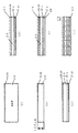
図1は、本発明の半導体装置の製造方法の実施例1にかかるIGBTの製造方法を説明するための主要な製造工程ごとの要部断面図である。以下の段落の文頭に示すアルファベット記号は図1内のアルファベット記号に対応させている。
a)400〜500μm程度の厚いFZ−n型シリコン半導体基板20に対して、おもて面に必要なpベース領域21、n+エミッタ領域22などの半導体領域をイオン注入および熱拡散により形成する。ゲート酸化膜23、ポリシリコンからなるゲート電極24の形成、BPSG(Boro Phospho Silicate Glass)やPSG(Phospho Silicate Glass)などの層間絶縁膜を形成する。
b)おもて面側にレジストなどの保護膜を形成後、ウエハの裏面側を研削加工して、耐圧に必要な厚さ(600V〜1200V耐圧の場合で、厚さ70μm〜200μm)程度、たとえば、140μm程度にまで、できるかぎり薄くする。研削後、研削面をフッ硝酸などのエッチング等により平滑化し洗浄する。この結果ウエハ厚さは約125μm程度の厚さになる。
c)裏面側の研削面にn型FS層26をP(リン)、Se(セレン)、S(イオウ)などのいずれかのイオン注入により、p+コレクタ層27をB(ボロン)のイオン注入によりそれぞれドープし、おもて面の前記保護膜を除去した後、800〜950℃程度の高温での活性化熱処理により機能領域とする。
FIG. 1 is a cross-sectional view of a main part for each main manufacturing process for explaining a manufacturing method of an IGBT according to Example 1 of a manufacturing method of a semiconductor device of the present invention. The alphabet symbols shown at the beginning of the following paragraphs correspond to the alphabet symbols in FIG.
a) For a thick FZ-n type
b) After forming a protective film such as a resist on the front surface side, the back surface side of the wafer is ground and processed to a thickness required for a withstand voltage (in the case of a withstand voltage of 600 V to 1200 V, a thickness of 70 μm to 200 μm), For example, the thickness is reduced to about 140 μm as much as possible. After grinding, the ground surface is smoothed and cleaned by etching such as hydrofluoric acid. As a result, the wafer thickness is about 125 μm.
c) The n-
d)おもて面へAl/Si,Cu合金をスパッタ蒸着により成膜する。フォトリソグラフィによりエミッタ電極膜25のパターンを形成する。エッチング液として燐酸・硝酸・酢酸などの混合液を用いる。枚葉式スピンエッチング装置を用いて、スピンナー上にウエハのおもて面を上にして吸着させ、500〜1000回転/分で回転させながら、フッ硝酸を1リットル/分の流量で滴下し、80秒〜100秒間エッチングする。このスピンエッチングにより、前記電極パターンエッチング後の下地のBPSGなどの層間絶縁膜上に残るSi析出物(およびまたはCu析出物)からなる残渣を除去する。この結果、Si析出物などからなる残渣の除去と共に、下地のBPSGも2000Å程度エッチングされ薄くなる。
このスピンエッチングによれば、エッチング液の裏面側への回り込みが無いので、ウエハの裏面側に保護膜形成する必要が無くなる。Si析出物などからなる残渣はBPSGなどの酸化膜系絶縁膜上に載っているので、フッ酸を含むエッチング液により、下地の上層部のエッチングと共に除去されやすい。続いて、純水で10秒間洗浄し、希フッ酸により短時間(10秒程度)スピンエッチングし、続いて60秒間純水で洗浄し乾燥してエミッタ電極膜25のパターンエッチングを完了させる。前記フッ硝酸による1段階目のスピンエッチングの際には、エッチング液を循環させて使用してもよいが、エッチングされたSi、Cuその他のものがエッチング液に溶解しているので、再度ウエハに付着する惧れがある。そこで、2段階目のスピンエッチングとして、希フッ酸によるスピンエッチングを短時間行うのである。従って、2段階目の希フッ酸のエッチング液は循環させて再使用せずにかけ流しとすることが好ましい。これ以降の工程は前述した従来のIGBTの製造方法と同じである。
d) An Al / Si, Cu alloy is formed on the front surface by sputter deposition. A pattern of the
According to this spin etching, there is no need to form a protective film on the back surface side of the wafer because the etching solution does not wrap around the back surface side. Residues made of Si deposits and the like are placed on an oxide film insulating film such as BPSG, and thus are easily removed together with the etching of the upper layer portion of the base by an etching solution containing hydrofluoric acid. Subsequently, the substrate is washed with pure water for 10 seconds, spin-etched with dilute hydrofluoric acid for a short time (about 10 seconds), subsequently washed with pure water for 60 seconds and dried to complete pattern etching of the
e)おもて面のエミッタ電極膜25面上に図示しない保護膜(ポリイミド膜)を塗布する。裏面側にコレクタ電極膜28を形成する。
f)接着テープ30にウエハのコレクタ電極膜面を下にして支持させ、ダイシングによりチップ29化する。
以上説明した実施例1によれば、ウエハの厚さを125μmという極めて薄くした場合に、片面にAl系合金からなるエミッタ電極膜を形成してウエハの反りが大きくなっても、ウエハ割れが増えたり、反りの影響で、おもて側の電極のパターニング処理時に裏面側がダメージを受けることなくIGBTを高良品率で生産効率よく製造することができる。
また、実施例1ではIGBTの製造方法について、本発明を適用した場合を説明したが、本発明はIGBTの製造方法に限られることなく、200μm以下の薄ウエハの片面にAl系合金電極膜を形成する工程を含む半導体装置の製造方法であれば、本発明を適用することにより、本発明の効果が得られる。
e) A protective film (polyimide film) (not shown) is applied on the surface of the
f) The
According to the first embodiment described above, even when the thickness of the wafer is extremely thin (125 μm), even if the warp of the wafer is increased by forming an emitter electrode film made of an Al-based alloy on one side, the wafer crack increases. Due to the influence of warping, the IGBT can be manufactured at a high yield rate with high yield without causing damage to the back side during patterning of the front electrode.
Moreover, although the case where this invention was applied about the manufacturing method of IGBT was demonstrated in Example 1, this invention is not restricted to the manufacturing method of IGBT, Al type alloy electrode film is provided on the single side | surface of a thin wafer of 200 micrometers or less. If it is a manufacturing method of a semiconductor device including the process of forming, the effect of the present invention will be acquired by applying the present invention.
20 シリコン半導体基板
21 pベース領域
22 n+エミッタ領域
23 ゲート酸化膜
24 ゲート電極
25 エミッタ電極膜
26 n型FS層
27 p+コレクタ層
28 コレクタ電極膜
29 チップ
30 接着テープ。
20 silicon semiconductor substrate 21 p base region 22 n + emitter region 23 gate oxide film 24
Claims (5)
5. The method for manufacturing a semiconductor device according to claim 1, wherein a dilute hydrofluoric acid, which is a second-stage chemical solution of the single-wafer spin etching solution, is discarded.
Priority Applications (1)
| Application Number | Priority Date | Filing Date | Title |
|---|---|---|---|
| JP2008098928A JP5018607B2 (en) | 2008-04-07 | 2008-04-07 | Manufacturing method of semiconductor device |
Applications Claiming Priority (1)
| Application Number | Priority Date | Filing Date | Title |
|---|---|---|---|
| JP2008098928A JP5018607B2 (en) | 2008-04-07 | 2008-04-07 | Manufacturing method of semiconductor device |
Publications (2)
| Publication Number | Publication Date |
|---|---|
| JP2009253000A true JP2009253000A (en) | 2009-10-29 |
| JP5018607B2 JP5018607B2 (en) | 2012-09-05 |
Family
ID=41313420
Family Applications (1)
| Application Number | Title | Priority Date | Filing Date |
|---|---|---|---|
| JP2008098928A Active JP5018607B2 (en) | 2008-04-07 | 2008-04-07 | Manufacturing method of semiconductor device |
Country Status (1)
| Country | Link |
|---|---|
| JP (1) | JP5018607B2 (en) |
Cited By (2)
| Publication number | Priority date | Publication date | Assignee | Title |
|---|---|---|---|---|
| JP2011191198A (en) * | 2010-03-15 | 2011-09-29 | Oki Semiconductor Co Ltd | Method for manufacturing semiconductor device |
| JP2012009629A (en) * | 2010-06-24 | 2012-01-12 | Fuji Electric Co Ltd | Semiconductor device manufacturing method |
Citations (5)
| Publication number | Priority date | Publication date | Assignee | Title |
|---|---|---|---|---|
| JPS62125633A (en) * | 1985-11-26 | 1987-06-06 | Seiko Epson Corp | Manufacture of semiconductor device |
| JPH02224233A (en) * | 1989-02-27 | 1990-09-06 | Hitachi Ltd | Sample treatment method end device |
| JPH0582505A (en) * | 1991-09-24 | 1993-04-02 | Matsushita Electric Ind Co Ltd | Etching method for metal thin film mainly composed of aluminum, and manufacture of thin film transistor |
| JPH0610161A (en) * | 1992-06-25 | 1994-01-18 | Matsushita Electric Ind Co Ltd | Etching solution composition for thin al-si film |
| JP2005236151A (en) * | 2004-02-23 | 2005-09-02 | Shindengen Electric Mfg Co Ltd | Manufacturing method of semiconductor device |
-
2008
- 2008-04-07 JP JP2008098928A patent/JP5018607B2/en active Active
Patent Citations (5)
| Publication number | Priority date | Publication date | Assignee | Title |
|---|---|---|---|---|
| JPS62125633A (en) * | 1985-11-26 | 1987-06-06 | Seiko Epson Corp | Manufacture of semiconductor device |
| JPH02224233A (en) * | 1989-02-27 | 1990-09-06 | Hitachi Ltd | Sample treatment method end device |
| JPH0582505A (en) * | 1991-09-24 | 1993-04-02 | Matsushita Electric Ind Co Ltd | Etching method for metal thin film mainly composed of aluminum, and manufacture of thin film transistor |
| JPH0610161A (en) * | 1992-06-25 | 1994-01-18 | Matsushita Electric Ind Co Ltd | Etching solution composition for thin al-si film |
| JP2005236151A (en) * | 2004-02-23 | 2005-09-02 | Shindengen Electric Mfg Co Ltd | Manufacturing method of semiconductor device |
Cited By (2)
| Publication number | Priority date | Publication date | Assignee | Title |
|---|---|---|---|---|
| JP2011191198A (en) * | 2010-03-15 | 2011-09-29 | Oki Semiconductor Co Ltd | Method for manufacturing semiconductor device |
| JP2012009629A (en) * | 2010-06-24 | 2012-01-12 | Fuji Electric Co Ltd | Semiconductor device manufacturing method |
Also Published As
| Publication number | Publication date |
|---|---|
| JP5018607B2 (en) | 2012-09-05 |
Similar Documents
| Publication | Publication Date | Title |
|---|---|---|
| JP3128811B2 (en) | Method for manufacturing semiconductor device | |
| JP5599342B2 (en) | Manufacturing method of semiconductor device | |
| JP4816278B2 (en) | Manufacturing method of semiconductor device | |
| US20140361384A1 (en) | Metal gate transistor and method for forming the same | |
| JP5018607B2 (en) | Manufacturing method of semiconductor device | |
| JP5011740B2 (en) | Manufacturing method of semiconductor device | |
| TW200522190A (en) | Wet cleaning method to eliminate copper corrosion | |
| JPS6364057B2 (en) | ||
| JP5884585B2 (en) | Method for manufacturing silicon carbide semiconductor device | |
| CN110473775A (en) | Improve the method for film removing | |
| JP2013115404A (en) | Semiconductor device manufacturing method | |
| JP6268767B2 (en) | Manufacturing method of semiconductor device | |
| CN116230525B (en) | Wafer Cleaning Method | |
| JP3413098B2 (en) | Dry etching substrate surface treatment method and apparatus | |
| JPH10242075A (en) | Manufacture of semiconductor device | |
| JP2002353236A (en) | Method for manufacturing poly silicon thin film transistor | |
| JP2007266347A (en) | Method of manufacturing semiconductor device | |
| JPH0150098B2 (en) | ||
| JP2001176872A (en) | Method for manufacturing semiconductor device | |
| JPS61258434A (en) | Manufacture of semiconductor device | |
| JPS59182568A (en) | Manufacture of insulated gate type field-effect semiconductor device | |
| CN114121631A (en) | Manufacturing method of SGT shielding grid | |
| JPS5922373B2 (en) | Semiconductor wafer processing method | |
| US6319812B1 (en) | Method of manufacturing a semiconductor device | |
| JP2005260032A (en) | Semiconductor device manufacturing method |
Legal Events
| Date | Code | Title | Description |
|---|---|---|---|
| A711 | Notification of change in applicant |
Free format text: JAPANESE INTERMEDIATE CODE: A712 Effective date: 20091112 |
|
| A625 | Written request for application examination (by other person) |
Free format text: JAPANESE INTERMEDIATE CODE: A625 Effective date: 20110315 |
|
| A711 | Notification of change in applicant |
Free format text: JAPANESE INTERMEDIATE CODE: A712 Effective date: 20110422 |
|
| A977 | Report on retrieval |
Free format text: JAPANESE INTERMEDIATE CODE: A971007 Effective date: 20120425 |
|
| TRDD | Decision of grant or rejection written | ||
| A01 | Written decision to grant a patent or to grant a registration (utility model) |
Free format text: JAPANESE INTERMEDIATE CODE: A01 Effective date: 20120515 |
|
| A01 | Written decision to grant a patent or to grant a registration (utility model) |
Free format text: JAPANESE INTERMEDIATE CODE: A01 |
|
| A61 | First payment of annual fees (during grant procedure) |
Free format text: JAPANESE INTERMEDIATE CODE: A61 Effective date: 20120528 |
|
| R150 | Certificate of patent or registration of utility model |
Ref document number: 5018607 Country of ref document: JP Free format text: JAPANESE INTERMEDIATE CODE: R150 Free format text: JAPANESE INTERMEDIATE CODE: R150 |
|
| FPAY | Renewal fee payment (event date is renewal date of database) |
Free format text: PAYMENT UNTIL: 20150622 Year of fee payment: 3 |
|
| R250 | Receipt of annual fees |
Free format text: JAPANESE INTERMEDIATE CODE: R250 |
|
| R250 | Receipt of annual fees |
Free format text: JAPANESE INTERMEDIATE CODE: R250 |
|
| R250 | Receipt of annual fees |
Free format text: JAPANESE INTERMEDIATE CODE: R250 |
|
| R250 | Receipt of annual fees |
Free format text: JAPANESE INTERMEDIATE CODE: R250 |
|
| R250 | Receipt of annual fees |
Free format text: JAPANESE INTERMEDIATE CODE: R250 |
|
| R250 | Receipt of annual fees |
Free format text: JAPANESE INTERMEDIATE CODE: R250 |
|
| R250 | Receipt of annual fees |
Free format text: JAPANESE INTERMEDIATE CODE: R250 |
|
| R250 | Receipt of annual fees |
Free format text: JAPANESE INTERMEDIATE CODE: R250 |
|
| R250 | Receipt of annual fees |
Free format text: JAPANESE INTERMEDIATE CODE: R250 |