JP2009231635A - Wiring board and its manufacturing method, semiconductor device, and its manufacturing method - Google Patents
Wiring board and its manufacturing method, semiconductor device, and its manufacturing method Download PDFInfo
- Publication number
- JP2009231635A JP2009231635A JP2008076775A JP2008076775A JP2009231635A JP 2009231635 A JP2009231635 A JP 2009231635A JP 2008076775 A JP2008076775 A JP 2008076775A JP 2008076775 A JP2008076775 A JP 2008076775A JP 2009231635 A JP2009231635 A JP 2009231635A
- Authority
- JP
- Japan
- Prior art keywords
- stiffener
- semiconductor chip
- chip
- wiring structure
- base material
- Prior art date
- Legal status (The legal status is an assumption and is not a legal conclusion. Google has not performed a legal analysis and makes no representation as to the accuracy of the status listed.)
- Pending
Links
Images


Classifications
-
- H—ELECTRICITY
- H01—ELECTRIC ELEMENTS
- H01L—SEMICONDUCTOR DEVICES NOT COVERED BY CLASS H10
- H01L21/00—Processes or apparatus adapted for the manufacture or treatment of semiconductor or solid state devices or of parts thereof
- H01L21/02—Manufacture or treatment of semiconductor devices or of parts thereof
- H01L21/04—Manufacture or treatment of semiconductor devices or of parts thereof the devices having at least one potential-jump barrier or surface barrier, e.g. PN junction, depletion layer or carrier concentration layer
- H01L21/48—Manufacture or treatment of parts, e.g. containers, prior to assembly of the devices, using processes not provided for in a single one of the subgroups H01L21/06 - H01L21/326
- H01L21/4814—Conductive parts
- H01L21/4846—Leads on or in insulating or insulated substrates, e.g. metallisation
- H01L21/4857—Multilayer substrates
-
- H—ELECTRICITY
- H01—ELECTRIC ELEMENTS
- H01L—SEMICONDUCTOR DEVICES NOT COVERED BY CLASS H10
- H01L23/00—Details of semiconductor or other solid state devices
- H01L23/16—Fillings or auxiliary members in containers or encapsulations, e.g. centering rings
-
- H—ELECTRICITY
- H01—ELECTRIC ELEMENTS
- H01L—SEMICONDUCTOR DEVICES NOT COVERED BY CLASS H10
- H01L23/00—Details of semiconductor or other solid state devices
- H01L23/48—Arrangements for conducting electric current to or from the solid state body in operation, e.g. leads, terminal arrangements ; Selection of materials therefor
- H01L23/488—Arrangements for conducting electric current to or from the solid state body in operation, e.g. leads, terminal arrangements ; Selection of materials therefor consisting of soldered or bonded constructions
- H01L23/498—Leads, i.e. metallisations or lead-frames on insulating substrates, e.g. chip carriers
- H01L23/49833—Leads, i.e. metallisations or lead-frames on insulating substrates, e.g. chip carriers the chip support structure consisting of a plurality of insulating substrates
-
- H—ELECTRICITY
- H01—ELECTRIC ELEMENTS
- H01L—SEMICONDUCTOR DEVICES NOT COVERED BY CLASS H10
- H01L2221/00—Processes or apparatus adapted for the manufacture or treatment of semiconductor or solid state devices or of parts thereof covered by H01L21/00
- H01L2221/67—Apparatus for handling semiconductor or electric solid state devices during manufacture or treatment thereof; Apparatus for handling wafers during manufacture or treatment of semiconductor or electric solid state devices or components; Apparatus not specifically provided for elsewhere
- H01L2221/683—Apparatus for handling semiconductor or electric solid state devices during manufacture or treatment thereof; Apparatus for handling wafers during manufacture or treatment of semiconductor or electric solid state devices or components; Apparatus not specifically provided for elsewhere for supporting or gripping
- H01L2221/68304—Apparatus for handling semiconductor or electric solid state devices during manufacture or treatment thereof; Apparatus for handling wafers during manufacture or treatment of semiconductor or electric solid state devices or components; Apparatus not specifically provided for elsewhere for supporting or gripping using temporarily an auxiliary support
- H01L2221/68345—Apparatus for handling semiconductor or electric solid state devices during manufacture or treatment thereof; Apparatus for handling wafers during manufacture or treatment of semiconductor or electric solid state devices or components; Apparatus not specifically provided for elsewhere for supporting or gripping using temporarily an auxiliary support used as a support during the manufacture of self supporting substrates
-
- H—ELECTRICITY
- H01—ELECTRIC ELEMENTS
- H01L—SEMICONDUCTOR DEVICES NOT COVERED BY CLASS H10
- H01L2224/00—Indexing scheme for arrangements for connecting or disconnecting semiconductor or solid-state bodies and methods related thereto as covered by H01L24/00
- H01L2224/01—Means for bonding being attached to, or being formed on, the surface to be connected, e.g. chip-to-package, die-attach, "first-level" interconnects; Manufacturing methods related thereto
- H01L2224/02—Bonding areas; Manufacturing methods related thereto
- H01L2224/04—Structure, shape, material or disposition of the bonding areas prior to the connecting process
- H01L2224/05—Structure, shape, material or disposition of the bonding areas prior to the connecting process of an individual bonding area
- H01L2224/0554—External layer
- H01L2224/0556—Disposition
- H01L2224/05571—Disposition the external layer being disposed in a recess of the surface
-
- H—ELECTRICITY
- H01—ELECTRIC ELEMENTS
- H01L—SEMICONDUCTOR DEVICES NOT COVERED BY CLASS H10
- H01L2224/00—Indexing scheme for arrangements for connecting or disconnecting semiconductor or solid-state bodies and methods related thereto as covered by H01L24/00
- H01L2224/01—Means for bonding being attached to, or being formed on, the surface to be connected, e.g. chip-to-package, die-attach, "first-level" interconnects; Manufacturing methods related thereto
- H01L2224/02—Bonding areas; Manufacturing methods related thereto
- H01L2224/04—Structure, shape, material or disposition of the bonding areas prior to the connecting process
- H01L2224/05—Structure, shape, material or disposition of the bonding areas prior to the connecting process of an individual bonding area
- H01L2224/0554—External layer
- H01L2224/05573—Single external layer
-
- H—ELECTRICITY
- H01—ELECTRIC ELEMENTS
- H01L—SEMICONDUCTOR DEVICES NOT COVERED BY CLASS H10
- H01L2224/00—Indexing scheme for arrangements for connecting or disconnecting semiconductor or solid-state bodies and methods related thereto as covered by H01L24/00
- H01L2224/01—Means for bonding being attached to, or being formed on, the surface to be connected, e.g. chip-to-package, die-attach, "first-level" interconnects; Manufacturing methods related thereto
- H01L2224/10—Bump connectors; Manufacturing methods related thereto
- H01L2224/11—Manufacturing methods
- H01L2224/11001—Involving a temporary auxiliary member not forming part of the manufacturing apparatus, e.g. removable or sacrificial coating, film or substrate
- H01L2224/11003—Involving a temporary auxiliary member not forming part of the manufacturing apparatus, e.g. removable or sacrificial coating, film or substrate for holding or transferring the bump preform
-
- H—ELECTRICITY
- H01—ELECTRIC ELEMENTS
- H01L—SEMICONDUCTOR DEVICES NOT COVERED BY CLASS H10
- H01L2224/00—Indexing scheme for arrangements for connecting or disconnecting semiconductor or solid-state bodies and methods related thereto as covered by H01L24/00
- H01L2224/01—Means for bonding being attached to, or being formed on, the surface to be connected, e.g. chip-to-package, die-attach, "first-level" interconnects; Manufacturing methods related thereto
- H01L2224/10—Bump connectors; Manufacturing methods related thereto
- H01L2224/15—Structure, shape, material or disposition of the bump connectors after the connecting process
- H01L2224/16—Structure, shape, material or disposition of the bump connectors after the connecting process of an individual bump connector
-
- H—ELECTRICITY
- H01—ELECTRIC ELEMENTS
- H01L—SEMICONDUCTOR DEVICES NOT COVERED BY CLASS H10
- H01L23/00—Details of semiconductor or other solid state devices
- H01L23/28—Encapsulations, e.g. encapsulating layers, coatings, e.g. for protection
- H01L23/31—Encapsulations, e.g. encapsulating layers, coatings, e.g. for protection characterised by the arrangement or shape
- H01L23/3107—Encapsulations, e.g. encapsulating layers, coatings, e.g. for protection characterised by the arrangement or shape the device being completely enclosed
- H01L23/3121—Encapsulations, e.g. encapsulating layers, coatings, e.g. for protection characterised by the arrangement or shape the device being completely enclosed a substrate forming part of the encapsulation
-
- H—ELECTRICITY
- H01—ELECTRIC ELEMENTS
- H01L—SEMICONDUCTOR DEVICES NOT COVERED BY CLASS H10
- H01L2924/00—Indexing scheme for arrangements or methods for connecting or disconnecting semiconductor or solid-state bodies as covered by H01L24/00
- H01L2924/0001—Technical content checked by a classifier
- H01L2924/00014—Technical content checked by a classifier the subject-matter covered by the group, the symbol of which is combined with the symbol of this group, being disclosed without further technical details
-
- H—ELECTRICITY
- H01—ELECTRIC ELEMENTS
- H01L—SEMICONDUCTOR DEVICES NOT COVERED BY CLASS H10
- H01L2924/00—Indexing scheme for arrangements or methods for connecting or disconnecting semiconductor or solid-state bodies as covered by H01L24/00
- H01L2924/01—Chemical elements
- H01L2924/01046—Palladium [Pd]
-
- H—ELECTRICITY
- H01—ELECTRIC ELEMENTS
- H01L—SEMICONDUCTOR DEVICES NOT COVERED BY CLASS H10
- H01L2924/00—Indexing scheme for arrangements or methods for connecting or disconnecting semiconductor or solid-state bodies as covered by H01L24/00
- H01L2924/01—Chemical elements
- H01L2924/01078—Platinum [Pt]
-
- H—ELECTRICITY
- H01—ELECTRIC ELEMENTS
- H01L—SEMICONDUCTOR DEVICES NOT COVERED BY CLASS H10
- H01L2924/00—Indexing scheme for arrangements or methods for connecting or disconnecting semiconductor or solid-state bodies as covered by H01L24/00
- H01L2924/01—Chemical elements
- H01L2924/01079—Gold [Au]
-
- H—ELECTRICITY
- H01—ELECTRIC ELEMENTS
- H01L—SEMICONDUCTOR DEVICES NOT COVERED BY CLASS H10
- H01L2924/00—Indexing scheme for arrangements or methods for connecting or disconnecting semiconductor or solid-state bodies as covered by H01L24/00
- H01L2924/15—Details of package parts other than the semiconductor or other solid state devices to be connected
- H01L2924/151—Die mounting substrate
- H01L2924/1515—Shape
- H01L2924/15153—Shape the die mounting substrate comprising a recess for hosting the device
-
- H—ELECTRICITY
- H01—ELECTRIC ELEMENTS
- H01L—SEMICONDUCTOR DEVICES NOT COVERED BY CLASS H10
- H01L2924/00—Indexing scheme for arrangements or methods for connecting or disconnecting semiconductor or solid-state bodies as covered by H01L24/00
- H01L2924/15—Details of package parts other than the semiconductor or other solid state devices to be connected
- H01L2924/151—Die mounting substrate
- H01L2924/1517—Multilayer substrate
- H01L2924/15172—Fan-out arrangement of the internal vias
- H01L2924/15174—Fan-out arrangement of the internal vias in different layers of the multilayer substrate
Landscapes
- Engineering & Computer Science (AREA)
- Physics & Mathematics (AREA)
- Condensed Matter Physics & Semiconductors (AREA)
- General Physics & Mathematics (AREA)
- Computer Hardware Design (AREA)
- Microelectronics & Electronic Packaging (AREA)
- Power Engineering (AREA)
- Ceramic Engineering (AREA)
- Manufacturing & Machinery (AREA)
- Wire Bonding (AREA)
- Production Of Multi-Layered Print Wiring Board (AREA)
Abstract
Description
本発明は、配線基板及びその製造方法、及び半導体装置及びその製造方法に関し、特に、半導体チップが実装される多層配線構造体と、多層配線構造体に設けられたスティフナーとを備えた配線基板及びその製造方法、及び半導体装置及びその製造方法に関する。 The present invention relates to a wiring board and a manufacturing method thereof, and a semiconductor device and a manufacturing method thereof, and in particular, a wiring board including a multilayer wiring structure on which a semiconductor chip is mounted, and a stiffener provided on the multilayer wiring structure. The present invention relates to a manufacturing method thereof, a semiconductor device, and a manufacturing method thereof.
従来の半導体装置(半導体パッケージ)は、半導体チップと、半導体チップがフリップチップ実装される多層配線構造体及び多層配線構造体に接着されたスティフナーを有する配線基板と、を有する。 A conventional semiconductor device (semiconductor package) includes a semiconductor chip, a multilayer wiring structure on which the semiconductor chip is flip-chip mounted, and a wiring substrate having a stiffener bonded to the multilayer wiring structure.
半導体チップは、半導体基板(例えば、シリコン基板(熱膨張係数3〜4ppm/℃))と、半導体基板に形成された半導体集積回路と、半導体集積回路と電気的に接続された電極パッドとを有する。
The semiconductor chip has a semiconductor substrate (for example, a silicon substrate (
多層配線構造体は、複数の樹脂層(熱膨張係数は55ppm/℃)が積層された樹脂層積層体と、樹脂層積層体に設けられ、半導体チップと電気的に接続される配線パターンと、配線パターンと電気的に接続されると共に、半導体チップが実装されるチップ実装用パッドとを有する。多層配線構造体としては、例えば、コアレス基板を用いることができる。多層配線構造体としてコアレス基板を用いた場合、多層配線構造体は、ビッドアップ法により、支持体となるCu板(熱膨張係数は18ppm/℃)上に多層配線構造体を形成し、その後、Cu板をエッチングにより除去することで形成する。ビッドアップ法では、加熱処理や冷却処理を繰り返し行う。 The multilayer wiring structure includes a resin layer laminate in which a plurality of resin layers (thermal expansion coefficient is 55 ppm / ° C.), a wiring pattern provided in the resin layer laminate and electrically connected to the semiconductor chip, It has a chip mounting pad on which a semiconductor chip is mounted while being electrically connected to the wiring pattern. As the multilayer wiring structure, for example, a coreless substrate can be used. When a coreless substrate is used as the multilayer wiring structure, the multilayer wiring structure is formed by forming a multilayer wiring structure on a Cu plate (thermal expansion coefficient: 18 ppm / ° C.) serving as a support by a bid-up method. It is formed by removing the Cu plate by etching. In the bid-up method, heat treatment and cooling treatment are repeated.
スティフナーは、多層配線構造体に実装された半導体チップを収容するための貫通部を有する。スティフナーは、コアレス基板の反りや歪みを低減するための部材である。スティフナーは、多層配線構造体とは別の製造工程で形成されており、接着剤により、支持体であるCu板が除去された多層配線構造体に接着されている。スティフナーの材料としては、NiやCu等の金属が用いられる(例えば、特許文献1参照。)。
しかしながら、従来の半導体装置では、半導体チップと金属からなるスティフナーとの熱膨張係数が異なるため、例えば、マザーボード等の実装基板に半導体装置を実装する場合、実装時の加熱により多層配線構造体が伸縮して、半導体装置と実装基板との間の電気的接続信頼性が低下してしまうという問題があった。 However, in the conventional semiconductor device, the coefficient of thermal expansion of the semiconductor chip and that of the metal stiffener are different. For example, when a semiconductor device is mounted on a mounting board such as a mother board, the multilayer wiring structure expands and contracts due to heating during mounting. As a result, there is a problem that the reliability of electrical connection between the semiconductor device and the mounting substrate is lowered.
また、従来の配線基板の製造方法では、支持体であるCu板の熱膨張係数が大きい(Cu板の熱膨張係数は18ppm/℃)ため、多層配線構造体の製造時に発生する多層配線構造体の反りや歪み(具体的には、樹脂層とCu板との熱膨張係数の差に起因する反りや歪み)を十分に低減することができない。そのため、半導体チップと配線基板との間の電気的接続信頼性が低下してしまうという問題があった。 Further, in the conventional method for manufacturing a wiring board, the Cu plate as a support has a large coefficient of thermal expansion (the Cu plate has a coefficient of thermal expansion of 18 ppm / ° C.), so that the multilayer wiring structure generated during the manufacture of the multilayer wiring structure Warpage and distortion (specifically, warpage and distortion caused by a difference in thermal expansion coefficient between the resin layer and the Cu plate) cannot be sufficiently reduced. For this reason, there is a problem in that the reliability of electrical connection between the semiconductor chip and the wiring board is lowered.
また、従来の配線基板の製造方法では、支持体であるCu板が除去された多層配線構造体にスティフナーを接着していたため、Cu板により抑制されていた反りや歪みが多層配線構造体に反映されてしまう。これにより、Cu板上に形成された多層配線構造体に設けられたチップ実装用パッドの位置と、Cu板が除去された多層配線構造体に設けられたチップ実装用パッドの位置との間にずれが生じてしまうため、半導体チップと配線基板との間の電気的接続信頼性が低下してしまうという問題があった。 Further, in the conventional method of manufacturing a wiring board, since the stiffener is bonded to the multilayer wiring structure from which the Cu plate as the support is removed, the warpage and distortion suppressed by the Cu plate are reflected in the multilayer wiring structure. It will be. Thereby, between the position of the chip mounting pad provided on the multilayer wiring structure formed on the Cu plate and the position of the chip mounting pad provided on the multilayer wiring structure from which the Cu plate is removed. Since the shift occurs, there is a problem that the reliability of electrical connection between the semiconductor chip and the wiring board is lowered.
なお、上記問題は、電極パッドが狭ピッチで配置された半導体チップを多層配線構造体のチップ実装用パッドに実装する場合に顕著となる。 The above problem becomes significant when a semiconductor chip having electrode pads arranged at a narrow pitch is mounted on a chip mounting pad of a multilayer wiring structure.
そこで本発明は、上述した問題点に鑑みなされたものであり、電気的接続信頼性を向上させることのできる配線基板及びその製造方法、及び半導体装置及びその製造方法を提供することを目的とする。 Therefore, the present invention has been made in view of the above-described problems, and an object thereof is to provide a wiring board and a manufacturing method thereof, a semiconductor device, and a manufacturing method thereof that can improve electrical connection reliability. .
本発明の一観点によれば、積層された複数の絶縁層と、前記複数の絶縁層に設けられた配線パターンと、前記配線パターンと電気的に接続されると共に、半導体チップがフリップチップ実装されるチップ実装用パッドと、を有する多層配線構造体と、前記半導体チップがフリップチップ実装される領域の外側に位置する部分の前記多層配線構造体に設けられたスティフナーと、を備えた配線基板であって、前記スティフナーの熱膨張係数は、前記半導体チップの熱膨張係数と略等しいことを特徴とする配線基板が提供される。 According to one aspect of the present invention, a plurality of stacked insulating layers, a wiring pattern provided in the plurality of insulating layers, a semiconductor chip is flip-chip mounted while being electrically connected to the wiring pattern. A wiring board comprising: a multilayer wiring structure having a chip mounting pad; and a stiffener provided in a portion of the multilayer wiring structure located outside a region where the semiconductor chip is flip-chip mounted. The wiring board is characterized in that the thermal expansion coefficient of the stiffener is substantially equal to the thermal expansion coefficient of the semiconductor chip.
本発明によれば、半導体チップがフリップチップ実装される領域の外側に位置する部分の多層配線構造体に設けられたスティフナーの熱膨張係数を、半導体チップの熱膨張係数と略等しくすることにより、半導体チップとスティフナーとが1枚の反り抑制基板として機能するため、多層配線構造体の反りや歪みを低減することが可能となる。これにより、例えば、配線基板をマザーボード等の実装基板に実装する場合、配線基板と実装基板との間の電気的接続信頼性を向上させることができる。 According to the present invention, by making the thermal expansion coefficient of the stiffener provided in the multilayer wiring structure in the portion located outside the region where the semiconductor chip is flip-chip mounted substantially equal to the thermal expansion coefficient of the semiconductor chip, Since the semiconductor chip and the stiffener function as a single warpage suppressing substrate, it is possible to reduce warpage and distortion of the multilayer wiring structure. Thereby, for example, when the wiring board is mounted on a mounting board such as a mother board, the electrical connection reliability between the wiring board and the mounting board can be improved.
本発明の他の観点によれば、半導体チップと、積層された複数の絶縁層、前記複数の絶縁層に設けられた配線パターン、及び前記配線パターンと電気的に接続されると共に、前記半導体チップがフリップチップ実装されたチップ実装用パッドを有する多層配線構造体と、前記半導体チップがフリップチップ実装される領域の外側に位置する部分の前記多層配線構造体に設けられたスティフナーとを有する配線基板と、を備えた半導体装置であって、前記スティフナーの熱膨張係数は、前記半導体チップの熱膨張係数と略等しいことを特徴とする半導体装置が提供される。 According to another aspect of the present invention, a semiconductor chip, a plurality of laminated insulating layers, a wiring pattern provided in the plurality of insulating layers, and the semiconductor chip are electrically connected to the wiring pattern and the semiconductor chip. Circuit board having a chip mounting pad on which the semiconductor chip is flip-chip mounted, and a stiffener provided on the multilayer wiring structure in a portion located outside the region where the semiconductor chip is flip-chip mounted The semiconductor device is characterized in that the thermal expansion coefficient of the stiffener is substantially equal to the thermal expansion coefficient of the semiconductor chip.
本発明によれば、半導体チップがフリップチップ実装される領域の外側に位置する部分の多層配線構造体に設けられたスティフナーの熱膨張係数を、半導体チップの熱膨張係数と略等しくすることにより、半導体チップとスティフナーとが1枚の反り抑制基板として機能するため、多層配線構造体の反りや歪みを低減することが可能となる。これにより、例えば、半導体装置をマザーボード等の実装基板に実装する場合、半導体装置と実装基板との間の電気的接続信頼性を向上させることができる。 According to the present invention, by making the thermal expansion coefficient of the stiffener provided in the multilayer wiring structure in the portion located outside the region where the semiconductor chip is flip-chip mounted substantially equal to the thermal expansion coefficient of the semiconductor chip, Since the semiconductor chip and the stiffener function as a single warpage suppressing substrate, it is possible to reduce warpage and distortion of the multilayer wiring structure. Thereby, for example, when the semiconductor device is mounted on a mounting substrate such as a mother board, the electrical connection reliability between the semiconductor device and the mounting substrate can be improved.
本発明のその他の観点によれば、電極パッドを有する半導体チップがフリップチップ実装されるチップ実装用パッドを備えた多層配線構造体と、前記半導体チップがフリップチップ実装される領域の外側に位置する部分の前記多層配線構造体に設けられ、前記半導体チップを収容する貫通部を有したスティフナーと、を備えた配線基板の製造方法であって、前記半導体チップと熱膨張係数が略等しく、前記貫通部を有するスティフナー母材を形成するスティフナー母材形成工程と、前記貫通部の形状に対応する凸部を有し、前記半導体チップと熱膨張係数が略等しい支持体を形成する支持体形成工程と、前記スティフナー母材に形成された前記貫通部に前記凸部を挿入して、前記スティフナー母材と前記支持体とを仮接着する仮接着工程と、前記凸部の上面、及び前記凸部の上面側に位置する前記スティフナー母材の面に、前記多層配線構造体を形成する多層配線構造体形成工程と、前記多層配線構造体形成工程後に前記スティフナー母材から前記支持体を取り外す支持体取外工程と、を含むことを特徴とする配線基板の製造方法が提供される。 According to another aspect of the present invention, a multilayer wiring structure including a chip mounting pad on which a semiconductor chip having an electrode pad is flip-chip mounted, and located outside a region where the semiconductor chip is flip-chip mounted. And a stiffener having a penetrating portion for accommodating the semiconductor chip, wherein the thermal expansion coefficient is substantially equal to that of the semiconductor chip and the penetrating portion is provided. A stiffener base material forming step for forming a stiffener base material having a portion, and a support body forming step for forming a support body having a convex portion corresponding to the shape of the penetrating portion and having a thermal expansion coefficient substantially equal to that of the semiconductor chip, A temporary bonding step of temporarily bonding the stiffener base material and the support by inserting the convex portion into the penetrating portion formed in the stiffener base material; A multilayer wiring structure forming step of forming the multilayer wiring structure on the upper surface of the convex portion and the surface of the stiffener base material positioned on the upper surface side of the convex portion; and the stiffener after the multilayer wiring structure forming step. And a support body removing step of removing the support body from the base material.
本発明によれば、半導体チップと熱膨張係数が略等しく、貫通部を有するスティフナー母材を形成し、貫通部の形状に対応する凸部を有し、半導体チップと熱膨張係数が略等しい支持体を形成し、次いで、スティフナー母材に形成された貫通部に凸部を挿入して、スティフナー母材と支持体とを仮接着し、次いで、凸部の上面、及び凸部の上面側に位置するスティフナー母材の面に、多層配線構造体を形成し、その後、スティフナー母材から支持体を取り外すことにより、スティフナーの母材であるスティフナー母材上に多層配線構造体が直接形成されるため、多層配線構造体から支持体を取り外した後も多層配線構造体14の反りや歪みを低減することが可能となる。これにより、多層配線構造体のチップ実装用パッドにフリップチップ実装される半導体チップと多層配線構造体との間の電気的接続信頼性を向上させることができる。
According to the present invention, the thermal expansion coefficient is substantially equal to that of the semiconductor chip, the stiffener base material having the penetration portion is formed, the convex portion corresponding to the shape of the penetration portion is provided, and the thermal expansion coefficient is substantially equal to that of the semiconductor chip. Then, a convex portion is inserted into the through portion formed in the stiffener base material, and the stiffener base material and the support are temporarily bonded, and then on the upper surface of the convex portion and the upper surface side of the convex portion. A multilayer wiring structure is formed on the surface of the stiffener base material, and then the support is removed from the stiffener base material, whereby the multilayer wiring structure is directly formed on the stiffener base material that is the base material of the stiffener. Therefore, it is possible to reduce warping and distortion of the
また、多層配線構造体の反りや歪みが低減されることにより、例えば、半導体装置をマザーボード等の実装基板に実装する場合、半導体装置と実装基板との間の電気的接続信頼性を向上させることができる。 In addition, by reducing warping and distortion of the multilayer wiring structure, for example, when mounting a semiconductor device on a mounting board such as a mother board, the electrical connection reliability between the semiconductor device and the mounting board is improved. Can do.
さらに、半導体チップを収容するスティフナー母材の貫通部に、半導体チップと熱膨張係数が略等しい凸部を挿入した状態で、凸部の上面、及び凸部の上面側に位置するスティフナー母材の面に多層配線構造体を形成することにより、半導体チップと熱膨張係数が略等しい凸部が半導体チップのダミーとして機能するため、予め半導体チップが搭載された状態で多層配線構造体を形成することが可能となる。これにより、半導体チップに設けられた電極パッドに対するチップ接続用パッドの位置ずれがなくなるため、チップ接続用パッドにフリップチップ実装される半導体チップと多層配線構造体との間の電気的な接続信頼性を向上させることができる。 Further, in the state where the convex portion having substantially the same thermal expansion coefficient as that of the semiconductor chip is inserted into the penetrating portion of the stiffener base material that accommodates the semiconductor chip, the upper surface of the convex portion and the stiffener base material positioned on the upper surface side of the convex portion By forming the multilayer wiring structure on the surface, the convex portion having substantially the same thermal expansion coefficient as the semiconductor chip functions as a dummy of the semiconductor chip. Therefore, the multilayer wiring structure is formed with the semiconductor chip mounted in advance. Is possible. As a result, the positional displacement of the chip connection pad with respect to the electrode pad provided on the semiconductor chip is eliminated, so that the electrical connection reliability between the semiconductor chip flip-chip mounted on the chip connection pad and the multilayer wiring structure Can be improved.
本発明によれば、半導体チップと多層配線構造体との間の電気的接続信頼性、及び/又は配線基板と実装基板との間の電気的接続信頼性を向上させることができる。 ADVANTAGE OF THE INVENTION According to this invention, the electrical connection reliability between a semiconductor chip and a multilayer wiring structure and / or the electrical connection reliability between a wiring board and a mounting board | substrate can be improved.
次に、図面に基づいて本発明の実施の形態について説明する。 Next, embodiments of the present invention will be described with reference to the drawings.
(第1の実施の形態)
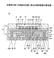
図1は、本発明の第1の実施の形態に係る半導体装置(半導体パッケージ)の断面図である。
(First embodiment)
FIG. 1 is a cross-sectional view of a semiconductor device (semiconductor package) according to a first embodiment of the present invention.
図1を参照するに、第1の実施の形態の半導体装置10は、配線基板11と、半導体チップ12とを有する。
Referring to FIG. 1, the
配線基板11は、多層配線構造体14と、スティフナー15とを有する。多層配線構造体14は、絶縁層17,21,24(積層された複数の絶縁層)と、チップ接続用パッド18と、配線パターン19,22,25と、はんだ20と、ソルダーレジスト層27とを有する。
The
絶縁層17は、半導体チップ12が実装されるチップ接続用パッド18と、配線パターン19とを形成するための層である。絶縁層17は、貫通孔29を有する。絶縁層17としては、例えば、樹脂層を用いることができる。樹脂層の材料としては、例えば、エポキシ樹脂やポリイミド樹脂等を用いることができる。
The
チップ接続用パッド18は、貫通孔29に設けられている。チップ接続用パッド18は、配線パターン19と一体的に構成されている。チップ接続用パッド18は、半導体チップ12をフリップチップ実装するためのパッドであり、半導体チップ12と電気的に接続されている。チップ接続用パッド18の接続面18Aは、絶縁層17の面17Aと略面一とされている。チップ接続用パッド18の接続面18Aは、はんだ20が形成される面である。チップ接続用パッド18の材料としては、例えば、Cuを用いることができる。
The
配線パターン19は、絶縁層17の面17B(面17Aとは反対側の絶縁層17の面)に設けられている。配線パターン19は、チップ接続用パッド18と電気的に接続されている。配線パターン19の材料としては、例えば、Cuを用いることができる。
The
はんだ20は、チップ接続用パッド18の接続面18Aに設けられている。はんだ20は、半導体チップ12の電極パッド48に設けられたバンプ23をチップ接続用パッド18上に固定するためのものである。はんだ20としては、例えば、Sn−Ag−Cu系はんだ、Sn−Zn−Bi系はんだ、Sn−Ag−In−Bi系はんだ、Sn−Ag−Cu−Ni系はんだ、Sn−Cu系はんだ、In等を用いることができる。
The
絶縁層21は、配線パターン19を覆うように、絶縁層17の面17Bに設けられている。絶縁層21は、配線パターン19の一部を露出する開口部34を有する。絶縁層21としては、例えば、樹脂層を用いることができる。樹脂層の材料としては、例えば、エポキシ樹脂やポリイミド樹脂等を用いることができる。
The insulating
配線パターン22は、ビア36と、ビア36と一体的に構成された配線37とを有する。ビア36は、開口部34に設けられている。ビア36は、その一方の端部が配線パターン19と接続されている。これにより、配線パターン22は、配線パターン19を介して、チップ接続用パッド18と電気的に接続されている。配線37は、絶縁層21の面21A(絶縁層17と接触する絶縁層21の面とは反対側の面)に設けられている。上記構成とされた配線パターン22の材料としては、例えば、Cuを用いることができる。
The
絶縁層24は、配線37を覆うように、絶縁層21の面21Aに設けられている。絶縁層24は、配線37の一部を露出する開口部39を有する。絶縁層24としては、例えば、樹脂層を用いることができる。樹脂層の材料としては、例えば、エポキシ樹脂やポリイミド樹脂等を用いることができる。
The insulating
配線パターン25は、ビア42と、ビア42と一体的に構成された外部接続用パッド43とを有する。ビア42は、開口部39に設けられている。ビア42は、その一方の端部が配線37と接続されている。これにより、配線パターン25は、配線バターン22と電気的に接続されている。外部接続用パッド43は、絶縁層24の面24A(絶縁層21と接触する絶縁層24の面とは反対側の面)に設けられている。外部接続用パッド43は、マザーボード等の実装基板と接続されるパッドである。外部接続用パッド43は、外部接続端子(図示せず)が配設される接続面43Aを有する。
The
ソルダーレジスト層27は、絶縁層24の面24Aに設けられている。ソルダーレジスト層27は、外部接続用パッド43の接続面43Aを露出する開口部45を有する。
The solder resist
スティフナー15は、半導体チップ12を収容するための貫通部47を有する。スティフナー15は、チップ実装領域A(半導体チップ12がフリップチップ実装される領域)の外側に位置する部分の絶縁層17の面17Aに接着されている。スティフナー15は、半導体チップ12の熱膨張係数(具体的には、半導体チップ12の構成要素の1つである半導体基板の熱膨張係数(半導体基板がシリコン基板の場合の熱膨張係数は3〜4ppm/℃))と熱膨張係数が略等しくなるように構成されている。
The
このように、半導体チップ12を収容するための貫通部47を有したスティフナー15の熱膨張係数を半導体チップ12の熱膨張係数と略等しくすることにより、半導体チップ12とスティフナー15とが1枚の反り抑制基板として機能するため、多層配線構造体14の反りや歪みを低減することが可能となる。これにより、例えば、配線基板11をマザーボード等の実装基板(図示せず)に実装する場合、配線基板11と実装基板との間の電気的接続信頼性を向上させることができる。
Thus, by making the thermal expansion coefficient of the
半導体チップ12がシリコン基板(熱膨張係数は3〜4ppm/℃)を備えた構成である場合、スティフナー15の熱膨張係数の値は、例えば、1〜5ppm/℃にすることができる。スティフナー15の材料としては、例えば、シリコン、CFRP(Carbon Fiber Reinforced Plastic)、インバーのうち、少なくとも1つの材料を用いることができる。なお、スティフナー15の材料は、上記材料に限定されない。
When the
半導体チップ12の厚さが30μm〜775μm、スティフナー15の材料としてシリコンを用いた場合、スティフナー15の厚さは、例えば、50μm〜775μmとすることができる。
When the thickness of the
半導体チップ12は、多層配線構造体14のチップ実装領域Aにフリップチップ実装されている。半導体チップ12は、図示していない半導体基板(例えば、シリコン基板)と、半導体基板に形成された半導体集積回路と、半導体集積回路と電気的に接続された電極パッド48とを有する。電極パッド48には、バンプ23(例えば、Auバンプ)が設けられている。バンプ23の下端部は、はんだ20によりチップ接続用パッド18に固定されている。これにより、電極パッド48は、チップ接続用パッド18と電気的に接続されている。半導体チップ12としては、例えば、CPU用半導体チップを用いることができる。
The
本実施の形態の半導体装置によれば、半導体チップ12を収容するための貫通部47を有したスティフナー15の熱膨張係数を半導体チップ12の熱膨張係数と略等しくすることにより、半導体チップ12とスティフナー15とが1枚の反り抑制基板として機能するため、多層配線構造体14の反りや歪みを低減することが可能となる。これにより、例えば、配線基板11をマザーボード等の実装基板(図示せず)に実装する場合、配線基板11と実装基板との間の電気的接続信頼性を向上させることができる。
According to the semiconductor device of the present embodiment, the thermal expansion coefficient of the
図2〜図26は、本発明の第1の実施の形態に係る半導体装置の製造工程を示す図である。図2〜図26において、第1の実施の形態の半導体装置10と同一構成部分には同一符号を付す。
2 to 26 are views showing manufacturing steps of the semiconductor device according to the first embodiment of the present invention. 2 to 26, the same components as those of the
図2〜図26を参照して、第1の実施の形態の半導体装置10の製造方法について説明する。始めに、図2に示す工程では、半導体チップ12と熱膨張係数が略等しい板体51を準備する。板体51は、スティフナー母材53の母材である。板体51は、スティフナー15が形成されるスティフナー形成領域Bを複数有する。スティフナー形成領域Bは、多層配線構造体14が形成される領域でもある。
A method for manufacturing the
半導体チップ12がシリコン基板(熱膨張係数は3〜4ppm/℃)を備えた構成とされている場合、板体51の熱膨張係数は、例えば、1〜5ppm/℃にすることができる。板体51の材料としては、例えば、シリコン、CFRP(Carbon Fiber Reinforced Plastic)、インバー等を用いることができる。板体51の材料としてシリコンを用いた場合、板体51の厚さは、例えば、200mmとすることができる。
When the
次いで、図3に示す工程では、スティフナー形成領域Bの中央に対応する部分の板体51に貫通部47を加工することで、スティフナー母材53を形成する(図2及び図3に示す工程が「スティフナー母材形成工程」に相当する工程)。貫通部47の側面47Aとスティフナー母材53の上面53Aとが成す角度は、略90度とされている。貫通部47は、例えば、板体51を機械加工(例えば、パンチ)することで形成する。
Next, in the step shown in FIG. 3, the
次いで、図4に示す工程では、半導体チップ12と略熱膨張係数が略等しい基板55を準備する。基板55は、スティフナー母材53の貫通部47に挿入される後述する支持体71の凸部61(図8参照)を複数形成するための部材である。基板55は、凸部61が形成される凸部形成領域Dを複数有する。基板55の熱膨張係数は、半導体チップ12の熱膨張係数と略等しい。基板55の材料としては、例えば、シリコン、ガラス、CFRP(Carbon Fiber Reinforced Plastic)、インバー等を用いることができる。基板55の材料としてシリコンを用いた場合、基板55の厚さは、例えば、500μmとすることができる。
Next, in the step shown in FIG. 4, a
次いで、図5に示す工程では、基板55の上面55Aに、開口部57Aを有したレジスト膜57を形成する。次いで、図6に示す工程では、レジスト膜57をマスクとするエッチングにより、基板55の上面55A側に複数の凹部59を形成する。凹部59は、はんだ20を配設するためのエリアである。上記エッチングとしては、例えば、ウエットエッチングやドライエッチング等を用いることができる。ドライエッチングとしては、例えば、ICPプラズマを用いて行うことができる。この場合のエッチングガスとしては、例えば、SF6ガスを用いることができる。
Next, in a step shown in FIG. 5, a resist
凹部59の配設ピッチは、半導体チップ12に設けられた電極パッド48の配設ピッチと略等しくなるように設定されている。凹部59の配設ピッチは、例えば、1μm〜50μmとすることができる。また、凹部59の深さは、例えば、1μm〜20μmとすることができる。
The arrangement pitch of the
次いで、図7に示す工程では、図6に示すレジスト膜57を除去する。次いで、図8に示す工程では、図7に示す構造体を切断位置Eに沿って切断する。これにより、後述する支持体71の凸部61が複数形成される。
Next, in the step shown in FIG. 7, the resist
次いで、図9に示す工程では、凸部61の表面全体(凹部59を構成する部分の凸部61の表面も含む)を覆うように金属膜63を形成する。金属膜63は、電解めっき法により、凹部59にはんだ20を形成する際の給電層となる膜である。金属膜63は、例えば、スパッタ法により形成することができる。金属膜63としては、例えば、凸部61の表面全体に、Ti膜(例えば、厚さ0.1μm)と、Cu膜(例えば、厚さ0.1μm)とを順次積層させたTi/Cu積層膜を用いることができる。
Next, in the step shown in FIG. 9, the
また、Ti/Cu積層膜の代わりに金属膜63として、例えば、はんだ20と合金を形成しにくい金属膜(具体的には、例えば、Al膜,Cr膜,Pt膜等)を用いてもよい。 Further, instead of the Ti / Cu laminated film, for example, a metal film that hardly forms an alloy with the solder 20 (specifically, for example, an Al film, a Cr film, a Pt film, or the like) may be used. .
このように、凹部59にはんだ20を形成する際の給電層となる金属膜63として、はんだ20と合金を形成しにくい金属膜(具体的には、例えば、Al膜,Cr膜,Pt膜等)を用いることにより、後述する図23に示す工程(支持体取外工程)において、金属膜63が形成された凸部61をはんだ20が形成された多層配線構造体14から取り外す際、金属膜63が形成された凸部61を容易に取り外すことができる。金属膜63としてAl膜を用いた場合、金属膜63の厚さは、例えば、0.5μmとすることができる。
As described above, as the
次いで、図10に示す工程では、金属膜63が形成された凸部61が配設される凸部配設領域Fを複数有すると共に、半導体チップ12の熱膨張係数と略等しい熱膨張係数とされた支持基板65を準備する。
Next, in the process shown in FIG. 10, the thermal expansion coefficient is set to be approximately equal to the thermal expansion coefficient of the
次いで、図11に示す工程では、支持基板65の上面65Aを覆うように金属膜66を成膜し、その後、凸部配設領域Fを除いた部分の金属膜66の一部をエッチングにより除去することで、アライメントマーク67を形成する。金属膜66は、電解めっき法によりはんだ20を形成する際、金属膜63に給電するための膜である。金属膜66としては、例えば、支持基板65の上面65Aに、Ti膜(例えば、厚さ0.1μm)と、Cu膜(例えば、厚さ0.1μm)とを順次積層させたTi/Cu積層膜を用いることができる。アライメントマーク67は、金属膜63が形成された凸部61を支持基板65の所定の領域(凸部配設領域F)に載置する際に使用するマークである。
Next, in the step shown in FIG. 11, a
次いで、図12に示す工程では、凸部配設領域Fに対応する部分の金属膜66上に金属膜63が形成された凸部61を接着して、凸部61に形成された金属膜63と、支持基板65に形成された金属膜66とを電気的に接続する。これにより、金属膜63が形成された複数の凸部61と、金属膜66が形成された支持基板65とを備えた支持体71が形成される(図4〜図12に示す工程が「支持体形成工程」に相当する工程)。金属膜63と金属膜66との接着には、例えば、導電性接着剤(例えば、Agペーストやカーボンテープ等)を用いることができる。
Next, in the process shown in FIG. 12, the
図12に示す工程では、金属膜66に形成されたアライメントマーク67を用いて、凸部配設領域Fに対応する部分の金属膜66上に、金属膜63が形成された凸部61を載置する。これにより、支持基板65の凸部配設領域Fに対して位置精度良く金属膜63が形成された凸部61を接着することができる。
In the step shown in FIG. 12, the
次いで、図13に示す工程では、スティフナー母材に設けられた貫通部47に、金属膜63が形成された凸部61を挿入して、スティフナー母材53と支持体71とを仮接着する(仮接着工程)。スティフナー母材53と支持体71との仮接着には、例えば、熱剥離タイプの両面テープを用いることができる。
Next, in the step shown in FIG. 13, the
次いで、図14に示す工程では、スティフナー母材53の上面53A、及び凹部59が設けられた側の凸部61に形成された金属膜63上に、複数の貫通孔29を有した絶縁層17を形成する。絶縁層17としては、例えば、樹脂層を用いることができる。また、樹脂層の材料としては、例えば、エポキシ樹脂やポリイミド樹脂等を用いることができる。絶縁層17として樹脂層を用いた場合、絶縁層17の厚さは、例えば、5μm〜30μmとすることができる。貫通孔29は、凹部59に形成された部分の金属膜63を露出するように形成する。貫通孔29は、例えば、レーザ加工により形成することができる。
Next, in the step shown in FIG. 14, the insulating
次いで、図15に示す工程では、金属膜63,66を給電層とする電解めっき法により、金属膜63が形成された凹部59を充填するようにはんだ20を形成する。はんだ20としては、例えば、Sn−Ag−Cu系はんだ、Sn−Zn−Bi系はんだ、Sn−Ag−In−Bi系はんだ、Sn−Ag−Cu−Ni系はんだ、Sn−Cu系はんだ、In等を用いることができる。
Next, in the step shown in FIG. 15, the
次いで、図16に示す工程では、はんだ20の上面20A、貫通孔29の側面に対応する部分の絶縁層17の面、及び絶縁層17の面17Bを覆うように、シード層73を形成する。具体的には、例えば、貫通孔29の側面に対応する部分の絶縁層17の面及び絶縁層17の面17Bをパラジウム処理した後、無電解めっき法によりめっき膜を析出成長させることでシード層73を形成する。シード層73としては、例えば、Cu層を用いることができる。シード層73としてCu層を用いた場合、シード層73の厚さは、例えば、0.1μmとすることができる。
Next, in the process shown in FIG. 16, the
次いで、図17に示す工程では、シード層73上に開口部74Aを有したレジスト膜74を形成する。開口部74Aは、チップ接続用パッド18及び配線パターン19の形成領域に対応する部分のシード層73の上面を露出するように形成する。
Next, in a step shown in FIG. 17, a resist
次いで、図18に示す工程では、シード層73を給電層とする電解めっき法により、開口部74Aに露出された部分のシード層73上にめっき膜76を析出成長させる。これにより、絶縁層17の貫通部29に、シード層73及びめっき膜76からなるチップ接続用パッド18が形成される。めっき膜76としては、例えば、Cuめっき膜を用いることができる。
Next, in the step shown in FIG. 18, a
次いで、図19に示す工程では、図18に示す構造体に設けられたレジスト膜74を除去する。次いで、図20に示す工程では、図19に示す構造体に設けられた不要な部分のシード層73(具体的には、めっき膜76に覆われていない部分のシード層73)を除去する。具体的には、例えば、ウエットエッチングにより、不要な部分のシード層73を除去する。これにより、絶縁層17の面17Bに、シード層73及びめっき膜76からなる配線パターン19が形成される。
Next, in a step shown in FIG. 19, the resist
次いで、図21に示す工程では、先に説明した図14〜図20に示す工程と同様な手法により、開口部34を有した絶縁層21と、配線パターン22と、開口部39を有した絶縁層24と、配線パターン25とを順次形成する。絶縁層21,24としては、例えば、樹脂層を用いることができる。また、樹脂層の材料としては、例えば、エポキシ樹脂やポリイミド樹脂等を用いることができる。絶縁層21,24として樹脂層を用いた場合、絶縁層21の厚さは、例えば、5μm〜30μm、絶縁層24の厚さは、例えば、5μm〜30μmとすることができる。開口部34,39は、例えば、レーザ加工により形成することができる。
Next, in the step shown in FIG. 21, the insulating
次いで、図22に示す工程では、絶縁層24の面24Aに、開口部45を有したソルダーレジスト層27を形成する。これにより、スティフナー形成領域Bに対応する部分のスティフナー母材53の上面53A及び凸部61上に多層配線構造体14が形成される(図14〜図22に示す工程が「多層配線構造体形成工程」に相当する工程である。)。この段階では、複数の多層配線構造体14は、一体的に構成されており、個片化されていない。
Next, in a step shown in FIG. 22, a solder resist
このように、半導体チップ12を収容するスティフナー母材53の貫通部47に、半導体チップ12と熱膨張係数が略等しい凸部61を挿入した状態で、凸部61の上面に形成された金属膜63、及び凸部61の上面側に位置するスティフナー母材53の面53Aに多層配線構造体14を形成することにより、半導体チップ12と熱膨張係数が略等しい凸部61が半導体チップ12のダミーとして機能するため、予め半導体チップ12が搭載された状態と同様に多層配線構造体14を形成することが可能となる。これにより、半導体チップ12に設けられた電極パッド48に対するチップ接続用パッド18の位置ずれがなくなるため、チップ接続用パッド18にフリップチップ実装される半導体チップ12と多層配線構造体14との間の電気的な接続信頼性を向上させることができる。
Thus, the metal film formed on the upper surface of the
次いで、図23に示す工程では、スティフナー母材53から支持体71を取り外す(支持体取外工程)。具体的には、例えば、スティフナー母材53と支持体71との接着に熱剥離タイプの両面テープを用いた場合、図22に示す構造体を加熱することで、スティフナー母材53から支持体71を取り外す。これにより、個片化されていない複数の配線基板11が形成される。
Next, in the step shown in FIG. 23, the support 71 is removed from the stiffener base material 53 (support removal step). Specifically, for example, when a heat-peeling type double-sided tape is used for bonding the
このように、複数の多層配線構造体14が形成されたスティフナー母材53から支持体71を取り外すことにより、多層配線構造体から支持体を取り外した後もスティフナー母材53により多層配線構造体14の反りや歪みを低減することが可能となる。これにより、多層配線構造体14のチップ実装用パッド18に半導体チップ12をフリップチップ実装した場合、半導体チップ12と多層配線構造体14との間の電気的接続信頼性を向上させることができる。
In this way, by removing the support 71 from the
また、多層配線構造体14の反りや歪みが低減されることにより、例えば、半導体装置10をマザーボード等の実装基板(図示せず)に実装する場合、半導体装置10と実装基板との間の電気的接続信頼性を向上させることができる。
In addition, since the warp and distortion of the
さらに、スティフナー母材53から取り外した支持体71は、他の複数の配線基板11を製造する際に再利用することが可能なため、支持体としてCu板を用いて多層配線構造体を形成する従来の手法(この場合、Cu板をエッチングにより除去するため再利用できない)と比較して、配線基板11の製造コストを低減することができる。
Furthermore, since the support body 71 removed from the
次いで、図24に示す工程では、図23に示すスティフナー母材53と、複数の多層配線構造体14とを備えた構造体の上下を反転させる。
Next, in the step shown in FIG. 24, the structure including the
次いで、図25に示す工程では、図24に示す構造体を切断位置Cに沿って切断することで、多層配線構造体14及びスティフナー15を個片する(切断工程)。これにより、複数の配線基板11が製造される。
Next, in the step shown in FIG. 25, the
このように、複数のスティフナー15の母材であるスティフナー母材53に、個片化されていない複数の多層配線構造体14を形成し、その後、個片化されていない複数の多層配線構造体14及びスティフナー母材53を切断位置Cに沿って切断することにより、一度に複数の複数の配線基板11を製造することができる。
In this way, a plurality of
次いで、図26に示す工程では、電極パッド48にバンプ23が形成された半導体チップ12を、多層配線構造体14のチップ接続用パッド18にフリップチップ実装する。これにより、第1の実施の形態の半導体装置10が製造される。
Next, in the step shown in FIG. 26, the
本実施の形態の半導体装置の製造方法によれば、半導体チップ12を収容するスティフナー母材53の貫通部47に、半導体チップ12と熱膨張係数が略等しい凸部61を挿入した状態で、凸部61の上面に形成された金属膜63、及び凸部61の上面側に位置するスティフナー母材53の面53Aに多層配線構造体14を形成することにより、半導体チップ12と熱膨張係数が略等しい凸部61が半導体チップ12のダミーとして機能するため、予め半導体チップ12が搭載された状態と同様に多層配線構造体14を形成することが可能となる。これにより、半導体チップ12に設けられた電極パッド48に対するチップ接続用パッド18の位置ずれがなくなるため、チップ接続用パッド18にフリップチップ実装される半導体チップ12と多層配線構造体14との間の電気的な接続信頼性を向上させることができる。
According to the method for manufacturing a semiconductor device of the present embodiment, a
また、複数の多層配線構造体14が形成されたスティフナー母材53から支持体71を取り外すことにより、多層配線構造体から支持体を取り外した後もスティフナー母材53により多層配線構造体14の反りや歪みを低減することが可能となる。これにより、多層配線構造体14のチップ実装用パッド18に半導体チップ12をフリップチップ実装した場合、半導体チップ12と多層配線構造体14との間の電気的接続信頼性を向上させることができる。
Further, by removing the support 71 from the
また、多層配線構造体14の反りや歪みが低減されることにより、例えば、半導体装置10をマザーボード等の実装基板(図示せず)に実装する場合、半導体装置10と実装基板との間の電気的接続信頼性を向上させることができる。
In addition, since the warp and distortion of the
さらに、スティフナー母材53から取り外した支持体71は、他の複数の配線基板11を製造する際に再利用することが可能なため、支持体としてCu板を用いて多層配線構造体を形成する従来の手法(この場合、Cu板をエッチングにより除去するため再利用できない)と比較して、配線基板11の製造コストを低減することができる。
Furthermore, since the support body 71 removed from the
なお、本実施の形態では、電解めっき法によりはんだ20を形成する場合を例に挙げて説明したが、インクジェット法によりはんだ20を形成してもよい。この場合、先に説明した図9に示す工程の処理が不要となるため、半導体装置10の製造コストを低減することができる。
In the present embodiment, the case where the
また、本実施の形態では、凸部61と支持基板65とが別体とされた支持体71を用いて半導体装置10を製造する場合を例に挙げて説明したが、凸部61と支持基板65とが一体的に構成された支持体を用いて、半導体装置10を製造してもよい。この場合、支持体の表面に一度で金属膜(電解めっき法により、はんだ20を形成する際の給電層となる金属膜)を形成することができる。
Further, in the present embodiment, the case where the
また、本実施の形態では、図15に示す工程において、凹部59を充填するよう、電解めっきにより、はんだ20を形成する場合を例に挙げて説明したが、はんだ20の代わりに、電解めっき法を用いて、はんだ以外の金属により凹部59を充填してバンプを形成してもよい。具体的には、電解めっき法により、凹部59の内壁に金層と、ニッケル層とを順次積層し、次いで、電解めっき法により、凹部59を充填するようにバンプ本体となる銅膜を形成し、そして、多層配線構造体形成後に、支持体を除去することで、銅膜からなるバンプ本体の表面をニッケル層が覆う(金層はニッケル層を覆う)バンプを形成する。このようなバンプを備えた配線基板に半導体チップ12を実装する場合、予め、バンプ表面にはんだペーストを形成した後、配線基板に半導体チップ12をフリップチップ接続する。
In the present embodiment, the case where the
また、本実施の形態では、スティフナー母材53の上面53Aと貫通部47の側面47Aとが成す角度が略90度となるように構成されたスティフナー母材53を用いて、半導体装置10を製造する場合を例に挙げて説明したが、スティフナー母材53の代わりに、図27に示すスティフナー母材79を用いて半導体装置10を製造してもよい。
In the present embodiment, the
図27は、他のスティフナー母材を説明するための図である。 FIG. 27 is a diagram for explaining another stiffener base material.
図27を参照するに、スティフナー母材79は、金属膜63が形成された凸部61が収容される貫通部81を有する。貫通部81の形状は、スティフナー母材79の上面79A(多層配線構造体14が形成される側)から下方(下面79B(支持体71が挿入される側))に向かうにつれて幅広形状とされている。
Referring to FIG. 27, the
このように、金属膜63が形成された凸部61が収容される貫通部81の形状を、スティフナー母材79の上面79A(多層配線構造体14が形成される側)からスティフナー母材79の下面79Bに向かうにつれて幅広形状とすることにより、支持体取外工程において、スティフナー母材79から支持体71を容易に取り外すことができる。
In this way, the shape of the through-
スティフナー母材79の上面79Aと貫通部81の側面81Aとが成す角度θは、例えば、1度〜30度とすることができる。スティフナー母材79は、半導体チップ12の熱膨張係数と略等しく、先に説明したスティフナー15と同様な材料により構成されている。
An angle θ formed by the
(第2の実施の形態)
図28は、本発明の第2の実施の形態に係る半導体装置(半導体パッケージ)の断面図である。図28において、第1の実施の形態の半導体装置10と同一構成部分には同一符号を付す。
(Second Embodiment)
FIG. 28 is a sectional view of a semiconductor device (semiconductor package) according to the second embodiment of the present invention. In FIG. 28, the same components as those of the
図28を参照するに、第2の実施の形態の半導体装置90は、第1の実施の形態の半導体装置10に設けられた配線基板11の代わりに配線基板91を設けた以外は、半導体装置10と同様に構成される。
Referring to FIG. 28, the
配線基板91は、配線基板11に設けられた多層配線構造体14の代わりに多層配線構造体92を設けた以外は配線基板11と同様に構成される。多層配線構造体92は、チップ接続用パッド18の厚さを薄くして、はんだ20を貫通孔29の一部に設けた(言い換えれば、はんだ20を絶縁層17間に配設した)以外は、多層配線構造体14と同様に構成される。
The
このような構成とされた第2の実施の形態の半導体装置90は、第1の実施の形態の半導体装置10と同様な効果を得ることができる。
The
また、貫通孔29間に位置する部分の絶縁層17がソルダーレジスト層として機能するため、隣り合うはんだ20が接触することを防止できる。特に、電極パッド48が狭ピッチで配置された半導体装置12を多層配線構造体92に実装する場合に有効である。
Moreover, since the insulating
図29〜図37は、本発明の第2の実施の形態に係る半導体装置の製造工程を示す図である。図29〜図37において、第2の実施の形態の半導体装置90と同一構成部分には同一符号を付す。
29 to 37 are views showing manufacturing steps of the semiconductor device according to the second embodiment of the present invention. 29 to 37, the same components as those of the
図29〜図37を参照して、第2の実施の形態の半導体装置90の製造方法について説明する。始めに、図29に示す工程では、第1の実施の形態で説明した図4に示す基板55を切断位置Eに沿って切断する。これにより、後述する支持体97の凸部95が複数形成される。複数の凸部95の上面95Aは、平坦な面とされている。
With reference to FIGS. 29 to 37, a method of manufacturing the
次いで、図30に示す工程では、凸部95の表面全体を覆うように金属膜63を形成する。次いで、図31に示す工程では、第1の実施の形態で説明した図11に示す構造体の凸部配設領域Fに対応する部分に形成された金属膜66上に、金属膜63が形成された凸部95を接着して、凸部95に形成された金属膜63と、支持基板65に形成された金属膜66とを電気的に接続する。これにより、金属膜63が形成された複数の凸部95と、金属膜66が形成された支持基板65とを備えた支持体97が形成される。
Next, in the step shown in FIG. 30, the
次いで、図32に示す工程では、スティフナー母材53に形成された貫通部47に、金属膜63が形成された凸部95を挿入して、スティフナー母材53と支持体97とを仮接着する(仮接着工程)。これにより、凸部95の上面95Aに設けられた金属膜63の上面とスティフナー母材53の上面53Aとが略面一となる。スティフナー母材53と支持体97との仮接着には、例えば、熱剥離タイプの両面テープを用いることができる。
Next, in the step shown in FIG. 32, the
次いで、図33に示す工程では、図32に示す構造体上に、複数の貫通孔29を有した絶縁層17を形成する。このとき、貫通孔29は、はんだ20の形成領域に対応する部分の金属膜63を露出するように形成する。絶縁層17は、第1の実施の形態で説明した図14に示す工程と同様な処理を行うことで形成する。
Next, in a step shown in FIG. 33, the insulating
次いで、図34に示す工程では、金属膜63,66を給電層とする電解めっき法により、貫通孔29に露出された部分の金属膜63上にはんだ20を形成する。はんだ20としては、例えば、Sn−Ag−Cu系はんだ、Sn−Zn−Bi系はんだ、Sn−Ag−In−Bi系はんだ、Sn−Ag−Cu−Ni系はんだ、Sn−Cu系はんだ、In等を用いることができる。また、はんだ20の厚さは、例えば、1μm〜20μmとすることができる。
Next, in the step shown in FIG. 34, the
次いで、図35に示す工程では、第1の実施の形態で説明した図16〜図23に示す工程と同様な処理を行うことで、個片化されていない複数の配線基板91を形成し、その後、個片化されていない複数の配線基板91の上下を反転させる。
Next, in the process shown in FIG. 35, by performing the same process as the process shown in FIGS. 16 to 23 described in the first embodiment, a plurality of
次いで、図36に示す工程では、図35に示す構造体を切断位置Cに沿って切断することで、多層配線構造体92及びスティフナー15を個片する(切断工程)。これにより、複数の配線基板11が個片化される。
Next, in the step shown in FIG. 36, the
次いで、図37に示す工程では、電極パッド48にバンプ23が形成された半導体チップ12を、多層配線構造体92に設けられたチップ接続用パッド18にフリップチップ実装する。これにより、第2の実施の形態の半導体装置90が製造される。
Next, in the step shown in FIG. 37, the
本実施の形態の半導体装置の製造方法によれば、凸部95の上面95A側にはんだ20を配設するための凹部59を形成する工程が不要となるため、半導体装置90の製造コストを低減することができる。
According to the manufacturing method of the semiconductor device of the present embodiment, the process of forming the
また、はんだ20が絶縁層17の貫通孔29に形成されるため、多層配線構造体92に設けられたチップ接続用パッド18に半導体チップ12をフリップチップ実装する際、隣り合うはんだ20が接触してショートすることを防止できる。
Further, since the
本実施の形態の半導体装置90の製造方法は、第1の実施の形態の半導体装置10の製造方法と同様な効果を得ることができる。
The manufacturing method of the
なお、本実施の形態では、電解めっき法によりはんだ20を形成する場合を例に挙げて説明したが、インクジェット法によりはんだ20を形成してもよい。この場合、先に説明した図30に示す工程の処理が不要となるため、半導体装置90の製造コストを低減することができる。
In the present embodiment, the case where the
また、本実施の形態では、凸部95と支持基板65とが別体とされた支持体97を用いて半導体装置90を製造する場合を例に挙げて説明したが、凸部95と支持基板65とが一体的に構成された支持体を用いて半導体装置90を製造してもよい。
In the present embodiment, the case where the
また、本実施の形態では、スティフナー母材53を用いて半導体装置90を製造する場合を例に挙げて説明したが、スティフナー母材53の代わりに第1の実施の形態で説明したスティフナー母材79(図27参照)を用いて半導体装置90を製造してもよい。
In this embodiment, the case where the
また、本実施の形態では、図34に示す工程において、金属膜63上にはんだ20を形成する場合を例に挙げて説明したが、はんだ20の代わりに、はんだ以外の金属からなるパッドを設けてもよい。具体的には、金属膜63上に、電解めっき法により、金層と、ニッケル層と、銅層とを順次積層させ、多層配線構造体形成後、支持体を除去することで、金層、ニッケル層、及び銅層からなるパッドを形成する。このようなパッドを有した配線基板に半導体チップ12を実装する場合、予め、パッド表面にはんだペーストを形成した後、配線基板に半導体チップ12をフリップチップ接続する。
In the present embodiment, the case where the
以上、本発明の好ましい実施の形態について詳述したが、本発明はかかる特定の実施の形態に限定されるものではなく、特許請求の範囲内に記載された本発明の要旨の範囲内において、種々の変形・変更が可能である。 The preferred embodiments of the present invention have been described in detail above, but the present invention is not limited to such specific embodiments, and within the scope of the present invention described in the claims, Various modifications and changes are possible.
本発明は、半導体チップが実装される多層配線構造体と、多層配線構造体に設けられたスティフナーとを備えた配線基板及びその製造方法、及び半導体装置及びその製造方法に適用できる。 The present invention can be applied to a wiring board including a multilayer wiring structure on which a semiconductor chip is mounted, a stiffener provided on the multilayer wiring structure, a manufacturing method thereof, a semiconductor device, and a manufacturing method thereof.
10,90 半導体装置
11,91 配線基板
12 半導体チップ
14,92 多層配線構造体
15 スティフナー
17,21,24 絶縁層
17A,17B,21A,24A 面
18 チップ接続用パッド
18A,43A 接続面
19,22,25 配線パターン
20 はんだ
20A,53A,55A,65A,79A,95A 上面
23 バンプ
27 ソルダーレジスト層
29 貫通孔
34,39,45,57A,74A 開口部
36,42 ビア
37 配線
43 外部接続用パッド
47,81 貫通部
47A,81A 側面
48 電極パッド
51 板体
53,79 スティフナー母材
55 基板
57,74 レジスト膜
59 凹部
61,95 凸部
63,66 金属膜
65 支持基板
67 アライメントマーク
71,97 支持体
73 シード層
76 めっき膜
79B 下面
A チップ実装領域
B スティフナー形成領域
C,E 切断位置
D 凸部形成領域
F 凸部配設領域
θ 角度
DESCRIPTION OF
Claims (10)
前記半導体チップがフリップチップ実装される領域の外側に位置する部分の前記多層配線構造体に設けられたスティフナーと、を備えた配線基板であって、
前記スティフナーの熱膨張係数は、前記半導体チップの熱膨張係数と略等しいことを特徴とする配線基板。 A plurality of laminated insulating layers; wiring patterns provided on the plurality of insulating layers; and chip mounting pads that are electrically connected to the wiring patterns and on which a semiconductor chip is flip-chip mounted. A multilayer wiring structure;
A stiffener provided on the multilayer wiring structure in a portion located outside a region where the semiconductor chip is flip-chip mounted,
The wiring board according to claim 1, wherein a thermal expansion coefficient of the stiffener is substantially equal to a thermal expansion coefficient of the semiconductor chip.
積層された複数の絶縁層、前記複数の絶縁層に設けられた配線パターン、及び前記配線パターンと電気的に接続されると共に、前記半導体チップがフリップチップ実装されたチップ実装用パッドを有する多層配線構造体と、前記半導体チップがフリップチップ実装される領域の外側に位置する部分の前記多層配線構造体に設けられたスティフナーとを有する配線基板と、を備えた半導体装置であって、
前記スティフナーの熱膨張係数は、前記半導体チップの熱膨張係数と略等しいことを特徴とする半導体装置。 A semiconductor chip;
Multi-layered wiring having a plurality of laminated insulating layers, wiring patterns provided in the plurality of insulating layers, and chip mounting pads that are electrically connected to the wiring patterns and on which the semiconductor chip is flip-chip mounted A wiring board having a structure and a stiffener provided in a portion of the multilayer wiring structure located outside a region where the semiconductor chip is flip-chip mounted,
The semiconductor device according to claim 1, wherein a thermal expansion coefficient of the stiffener is substantially equal to a thermal expansion coefficient of the semiconductor chip.
前記半導体チップと熱膨張係数が略等しく、前記貫通部を有するスティフナー母材を形成するスティフナー母材形成工程と、
前記貫通部の形状に対応する凸部を有し、前記半導体チップと熱膨張係数が略等しい支持体を形成する支持体形成工程と、
前記スティフナー母材に形成された前記貫通部に前記凸部を挿入して、前記スティフナー母材と前記支持体とを仮接着する仮接着工程と、
前記凸部の上面、及び前記凸部の上面側に位置する前記スティフナー母材の面に、前記多層配線構造体を形成する多層配線構造体形成工程と、
前記多層配線構造体形成工程後に前記スティフナー母材から前記支持体を取り外す支持体取外工程と、を含むことを特徴とする配線基板の製造方法。 Provided in a multilayer wiring structure having a chip mounting pad on which a semiconductor chip having an electrode pad is flip-chip mounted, and in a portion of the multilayer wiring structure located outside a region where the semiconductor chip is flip-chip mounted A stiffener having a penetrating portion for accommodating the semiconductor chip, and a method of manufacturing a wiring board comprising:
A stiffener base material forming step for forming a stiffener base material having a thermal expansion coefficient substantially equal to that of the semiconductor chip and having the penetrating portion;
A support forming step of forming a support having a convex portion corresponding to the shape of the penetrating portion and having a thermal expansion coefficient substantially equal to that of the semiconductor chip;
A temporary bonding step of inserting the convex portion into the penetrating portion formed in the stiffener base material and temporarily bonding the stiffener base material and the support;
A multilayer wiring structure forming step of forming the multilayer wiring structure on the upper surface of the convex portion and the surface of the stiffener base material located on the upper surface side of the convex portion;
A method of manufacturing a wiring board, comprising: a support body removing step of removing the support body from the stiffener base material after the multilayer wiring structure forming step.
前記スティフナー母材形成工程では、前記貫通部を複数形成し、前記支持体形成工程では、前記凸部を複数形成し、前記多層配線構造体形成工程では、個片化されていない複数の前記多層配線構造体を形成し、
前記支持体除去工程後に、前記スティフナー母材及び前記個片化されていない複数の多層配線構造体を切断する切断工程をさらに設けたことを特徴とする請求項5ないし7のうち、いずれか1項記載の配線基板の製造方法。 The stiffener base material has a plurality of stiffener forming regions where the stiffener is formed,
In the stiffener base material forming step, a plurality of the through portions are formed, in the supporting body forming step, the plurality of convex portions are formed, and in the multilayer wiring structure forming step, the plurality of non-separated multilayers Forming a wiring structure,
8. The method according to claim 5, further comprising a cutting step of cutting the stiffener base material and the plurality of undivided multilayer wiring structures after the support removing step. The manufacturing method of the wiring board of description.
Priority Applications (2)
| Application Number | Priority Date | Filing Date | Title |
|---|---|---|---|
| JP2008076775A JP2009231635A (en) | 2008-03-24 | 2008-03-24 | Wiring board and its manufacturing method, semiconductor device, and its manufacturing method |
| US12/408,853 US20090236727A1 (en) | 2008-03-24 | 2009-03-23 | Wiring substrate and method of manufacturing the same, and semiconductor device and method of manufacturing the same |
Applications Claiming Priority (1)
| Application Number | Priority Date | Filing Date | Title |
|---|---|---|---|
| JP2008076775A JP2009231635A (en) | 2008-03-24 | 2008-03-24 | Wiring board and its manufacturing method, semiconductor device, and its manufacturing method |
Publications (2)
| Publication Number | Publication Date |
|---|---|
| JP2009231635A true JP2009231635A (en) | 2009-10-08 |
| JP2009231635A5 JP2009231635A5 (en) | 2011-02-17 |
Family
ID=41088044
Family Applications (1)
| Application Number | Title | Priority Date | Filing Date |
|---|---|---|---|
| JP2008076775A Pending JP2009231635A (en) | 2008-03-24 | 2008-03-24 | Wiring board and its manufacturing method, semiconductor device, and its manufacturing method |
Country Status (2)
| Country | Link |
|---|---|
| US (1) | US20090236727A1 (en) |
| JP (1) | JP2009231635A (en) |
Cited By (3)
| Publication number | Priority date | Publication date | Assignee | Title |
|---|---|---|---|---|
| JP2013516060A (en) * | 2009-12-24 | 2013-05-09 | アイメック | Window interposed die packaging |
| JP2016105484A (en) * | 2012-12-20 | 2016-06-09 | インテル・コーポレーション | High density organic bridge device and method |
| JPWO2017057446A1 (en) * | 2015-10-02 | 2018-07-19 | 旭硝子株式会社 | Glass substrate, laminated substrate, and laminated body |
Families Citing this family (2)
| Publication number | Priority date | Publication date | Assignee | Title |
|---|---|---|---|---|
| WO2015013024A1 (en) * | 2013-07-22 | 2015-01-29 | Henkel IP & Holding GmbH | Methods to control wafer warpage upon compression molding thereof and articles useful therefor |
| KR102268781B1 (en) | 2014-11-12 | 2021-06-28 | 삼성전자주식회사 | Printed circuit board and method for manufacturing the same |
Citations (5)
| Publication number | Priority date | Publication date | Assignee | Title |
|---|---|---|---|---|
| JP2000323613A (en) * | 1999-03-11 | 2000-11-24 | Shinko Electric Ind Co Ltd | Multilayer substrate for semiconductor device and manufacture thereof |
| JP2004186265A (en) * | 2002-11-29 | 2004-07-02 | Ngk Spark Plug Co Ltd | Method for manufacturing multilayer wiring board |
| JP2005302922A (en) * | 2004-04-09 | 2005-10-27 | Ngk Spark Plug Co Ltd | Wiring board and its manufacturing method |
| WO2005114729A1 (en) * | 2004-05-21 | 2005-12-01 | Nec Corporation | Semiconductor device and wiring board |
| JP2008016508A (en) * | 2006-07-03 | 2008-01-24 | Nec Electronics Corp | Semiconductor device and its fabrication process |
Family Cites Families (16)
| Publication number | Priority date | Publication date | Assignee | Title |
|---|---|---|---|---|
| JP3267409B2 (en) * | 1992-11-24 | 2002-03-18 | 株式会社日立製作所 | Semiconductor integrated circuit device |
| US5919329A (en) * | 1997-10-14 | 1999-07-06 | Gore Enterprise Holdings, Inc. | Method for assembling an integrated circuit chip package having at least one semiconductor device |
| JP2001185653A (en) * | 1999-10-12 | 2001-07-06 | Fujitsu Ltd | Semiconductor device and method for manufacturing substrate |
| US6544812B1 (en) * | 2000-11-06 | 2003-04-08 | St Assembly Test Service Ltd. | Single unit automated assembly of flex enhanced ball grid array packages |
| JP3492348B2 (en) * | 2001-12-26 | 2004-02-03 | 新光電気工業株式会社 | Method of manufacturing package for semiconductor device |
| JP2004281830A (en) * | 2003-03-17 | 2004-10-07 | Shinko Electric Ind Co Ltd | Substrate for semiconductor device, method of manufacturing substrate, and semiconductor device |
| JP4057589B2 (en) * | 2003-03-25 | 2008-03-05 | 富士通株式会社 | Manufacturing method of electronic component mounting board |
| JP2004311768A (en) * | 2003-04-08 | 2004-11-04 | Shinko Electric Ind Co Ltd | Manufacturing method of substrate, substrate for semiconductor devices and semiconductor device |
| JP2004356569A (en) * | 2003-05-30 | 2004-12-16 | Shinko Electric Ind Co Ltd | Package for semiconductor device |
| US7094975B2 (en) * | 2003-11-20 | 2006-08-22 | Delphi Technologies, Inc. | Circuit board with localized stiffener for enhanced circuit component reliability |
| JP4205613B2 (en) * | 2004-03-01 | 2009-01-07 | エルピーダメモリ株式会社 | Semiconductor device |
| US20060118947A1 (en) * | 2004-12-03 | 2006-06-08 | Taiwan Semiconductor Manufacturing Co., Ltd. | Thermal expansion compensating flip chip ball grid array package structure |
| US7719021B2 (en) * | 2005-06-28 | 2010-05-18 | Lighting Science Group Corporation | Light efficient LED assembly including a shaped reflective cavity and method for making same |
| JP2007123524A (en) * | 2005-10-27 | 2007-05-17 | Shinko Electric Ind Co Ltd | Substrate with built-in electronic part |
| JP2008160019A (en) * | 2006-12-26 | 2008-07-10 | Shinko Electric Ind Co Ltd | Electronic component |
| US7750459B2 (en) * | 2008-02-01 | 2010-07-06 | International Business Machines Corporation | Integrated module for data processing system |
-
2008
- 2008-03-24 JP JP2008076775A patent/JP2009231635A/en active Pending
-
2009
- 2009-03-23 US US12/408,853 patent/US20090236727A1/en not_active Abandoned
Patent Citations (5)
| Publication number | Priority date | Publication date | Assignee | Title |
|---|---|---|---|---|
| JP2000323613A (en) * | 1999-03-11 | 2000-11-24 | Shinko Electric Ind Co Ltd | Multilayer substrate for semiconductor device and manufacture thereof |
| JP2004186265A (en) * | 2002-11-29 | 2004-07-02 | Ngk Spark Plug Co Ltd | Method for manufacturing multilayer wiring board |
| JP2005302922A (en) * | 2004-04-09 | 2005-10-27 | Ngk Spark Plug Co Ltd | Wiring board and its manufacturing method |
| WO2005114729A1 (en) * | 2004-05-21 | 2005-12-01 | Nec Corporation | Semiconductor device and wiring board |
| JP2008016508A (en) * | 2006-07-03 | 2008-01-24 | Nec Electronics Corp | Semiconductor device and its fabrication process |
Cited By (8)
| Publication number | Priority date | Publication date | Assignee | Title |
|---|---|---|---|---|
| JP2013516060A (en) * | 2009-12-24 | 2013-05-09 | アイメック | Window interposed die packaging |
| JP2017022398A (en) * | 2009-12-24 | 2017-01-26 | アイメックImec | Window interposed die packaging |
| JP2016105484A (en) * | 2012-12-20 | 2016-06-09 | インテル・コーポレーション | High density organic bridge device and method |
| US10103105B2 (en) | 2012-12-20 | 2018-10-16 | Intel Corporation | High density organic bridge device and method |
| US10672713B2 (en) | 2012-12-20 | 2020-06-02 | Intel Corporation | High density organic bridge device and method |
| JPWO2017057446A1 (en) * | 2015-10-02 | 2018-07-19 | 旭硝子株式会社 | Glass substrate, laminated substrate, and laminated body |
| US11180407B2 (en) | 2015-10-02 | 2021-11-23 | AGC Inc. | Glass substrate, laminated substrate, and laminate |
| US11753330B2 (en) | 2015-10-02 | 2023-09-12 | AGC Inc. | Glass substrate, laminated substrate, and laminate |
Also Published As
| Publication number | Publication date |
|---|---|
| US20090236727A1 (en) | 2009-09-24 |
Similar Documents
| Publication | Publication Date | Title |
|---|---|---|
| JP5224784B2 (en) | Wiring board and manufacturing method thereof | |
| JP5144222B2 (en) | Wiring board and manufacturing method thereof | |
| JP5114130B2 (en) | WIRING BOARD, MANUFACTURING METHOD THEREOF, AND SEMICONDUCTOR DEVICE | |
| US7937828B2 (en) | Method of manufacturing wiring board | |
| JP4541763B2 (en) | Circuit board manufacturing method | |
| US7377030B2 (en) | Wiring board manufacturing method | |
| US8609539B2 (en) | Embedded semiconductor device substrate and production method thereof | |
| JP4332162B2 (en) | Wiring board manufacturing method | |
| US8945329B2 (en) | Printed wiring board and method for manufacturing printed wiring board | |
| JP2008300507A (en) | Wiring substrate and manufacturing process of the same | |
| KR100992181B1 (en) | Packaging board and manufacturing method thereof | |
| JP2012169591A (en) | Multilayer wiring board | |
| US8479385B2 (en) | Method of producing wiring substrate | |
| JP2009231635A (en) | Wiring board and its manufacturing method, semiconductor device, and its manufacturing method | |
| JP2013540368A (en) | Printed circuit board and manufacturing method thereof | |
| JP2007149731A (en) | Wiring board, semiconductor device, and process for producing wiring board | |
| JP5386647B2 (en) | Wiring board | |
| JP5442192B2 (en) | Device mounting substrate, semiconductor module, and device mounting substrate manufacturing method | |
| KR102494340B1 (en) | Printed circuit board | |
| US11792937B2 (en) | Component built-in wiring substrate | |
| US20230135774A1 (en) | Interconnect substrate, method of manufacturing the same, and semiconductor apparatus | |
| JP2007324232A (en) | Bga-type multilayer wiring board and bga-type semiconductor package | |
| KR100815322B1 (en) | Printed circuit board and fabricating method of the same | |
| JP2006261382A (en) | Multilayer wiring board and its manufacturing method | |
| JP2008130618A (en) | Multilayer wiring board |
Legal Events
| Date | Code | Title | Description |
|---|---|---|---|
| A521 | Request for written amendment filed |
Free format text: JAPANESE INTERMEDIATE CODE: A523 Effective date: 20101220 |
|
| A621 | Written request for application examination |
Free format text: JAPANESE INTERMEDIATE CODE: A621 Effective date: 20101220 |
|
| A977 | Report on retrieval |
Free format text: JAPANESE INTERMEDIATE CODE: A971007 Effective date: 20110831 |
|
| A131 | Notification of reasons for refusal |
Free format text: JAPANESE INTERMEDIATE CODE: A131 Effective date: 20110906 |
|
| A521 | Request for written amendment filed |
Free format text: JAPANESE INTERMEDIATE CODE: A523 Effective date: 20111104 |
|
| A131 | Notification of reasons for refusal |
Free format text: JAPANESE INTERMEDIATE CODE: A131 Effective date: 20120221 |
|
| A02 | Decision of refusal |
Free format text: JAPANESE INTERMEDIATE CODE: A02 Effective date: 20120724 |