JP2009229247A - Photon detector having phase adjustment function and photon detection method - Google Patents
Photon detector having phase adjustment function and photon detection method Download PDFInfo
- Publication number
- JP2009229247A JP2009229247A JP2008074894A JP2008074894A JP2009229247A JP 2009229247 A JP2009229247 A JP 2009229247A JP 2008074894 A JP2008074894 A JP 2008074894A JP 2008074894 A JP2008074894 A JP 2008074894A JP 2009229247 A JP2009229247 A JP 2009229247A
- Authority
- JP
- Japan
- Prior art keywords
- waveform data
- phase
- photon detection
- identification
- waveform
- Prior art date
- Legal status (The legal status is an assumption and is not a legal conclusion. Google has not performed a legal analysis and makes no representation as to the accuracy of the status listed.)
- Withdrawn
Links
- 238000001514 detection method Methods 0.000 title claims abstract description 99
- 238000005070 sampling Methods 0.000 claims abstract description 71
- 238000012935 Averaging Methods 0.000 claims abstract description 21
- 238000000034 method Methods 0.000 claims description 12
- 230000000630 rising effect Effects 0.000 claims description 4
- 238000010586 diagram Methods 0.000 description 24
- 230000010363 phase shift Effects 0.000 description 7
- 230000006870 function Effects 0.000 description 5
- 230000015556 catabolic process Effects 0.000 description 2
- 150000001875 compounds Chemical class 0.000 description 2
- 230000006866 deterioration Effects 0.000 description 2
- 229910000530 Gallium indium arsenide Inorganic materials 0.000 description 1
- 230000005540 biological transmission Effects 0.000 description 1
- 230000000694 effects Effects 0.000 description 1
- 230000007274 generation of a signal involved in cell-cell signaling Effects 0.000 description 1
- 230000003287 optical effect Effects 0.000 description 1
- 239000013307 optical fiber Substances 0.000 description 1
- 230000003071 parasitic effect Effects 0.000 description 1
- 230000000737 periodic effect Effects 0.000 description 1
- 238000003672 processing method Methods 0.000 description 1
- 230000035945 sensitivity Effects 0.000 description 1
Images


Classifications
-
- G—PHYSICS
- G01—MEASURING; TESTING
- G01J—MEASUREMENT OF INTENSITY, VELOCITY, SPECTRAL CONTENT, POLARISATION, PHASE OR PULSE CHARACTERISTICS OF INFRARED, VISIBLE OR ULTRAVIOLET LIGHT; COLORIMETRY; RADIATION PYROMETRY
- G01J1/00—Photometry, e.g. photographic exposure meter
- G01J1/42—Photometry, e.g. photographic exposure meter using electric radiation detectors
- G01J1/44—Electric circuits
Landscapes
- Physics & Mathematics (AREA)
- General Physics & Mathematics (AREA)
- Spectroscopy & Molecular Physics (AREA)
- Photometry And Measurement Of Optical Pulse Characteristics (AREA)
Abstract
Description
本発明は、アバランシェ・フォトダイオード(Avalanche photodiode)等の単一光子検出可能な受光素子をゲートモードで駆動する光子検出回路に係り、特に受光素子の出力信号をサンプリングにより離散的なデータとして処理する光子検出回路および光子検出方法に関する。 The present invention relates to a photon detection circuit that drives a single-photon-detectable light-receiving element such as an avalanche photodiode in a gate mode, and particularly processes the output signal of the light-receiving element as discrete data by sampling. The present invention relates to a photon detection circuit and a photon detection method.
光子受信器において、単一光子を検出する素子としては、一般にアバランシェ・フォトダイオード(以下、APDと記す。)が用いられている。基本的には、APDのブレークダウン電圧(VBd)以上の逆バイアス電圧をAPDに印加することでAPDの増倍率を極めて大きくしておき、光子1個から生成する光電流を十分に大きな信号振幅まで増幅することで外部回路による処理を可能にしている。 In the photon receiver, an avalanche photodiode (hereinafter referred to as APD) is generally used as an element for detecting a single photon. Basically, by applying a reverse bias voltage equal to or higher than the breakdown voltage (VBd) of the APD to the APD, the multiplication factor of the APD is made extremely large, and the photocurrent generated from one photon has a sufficiently large signal amplitude. The processing by the external circuit is made possible by amplifying the signal up to.
光ファイバを用いた長距離単一光子伝送を行う為には、1.55um帯に感度を持つ化合物系のAPDが光子検出素子として最適である。非特許文献1に記載されるように、化合物APDを用いた単一光子検出器では、APD素子の冷却とゲートモードの適用が必須である。ゲートモードで駆動されたAPDから出力される光子検出信号は、ゲートパルスの微分波形に光子検出信号波形が重畳されて出力される。この微分波形はAPDのPNジャンクションの寄生容量に起因することから、チャージパルスとも呼ばれる。
In order to perform long-distance single photon transmission using an optical fiber, a compound APD having sensitivity in the 1.55 um band is optimal as a photon detection element. As described in Non-Patent
チャージパルスは、回路帯域の上昇に連れて大きな振幅として観測されるために、小振幅の光子検出信号の検出を阻害する。この問題を解決するための高精度なチャージパルス補償方式が非特許文献2〜4に提案されており、高感度な光子検出が実現可能になった。
Since the charge pulse is observed as a large amplitude as the circuit band increases, detection of a small-amplitude photon detection signal is hindered.
更に、非特許文献5および特許文献1には、上述したチャージパルス補償回路において、素子の個体差に起因したチャージパルス補償誤差の問題が存在する事を指摘し、その解決方法を提案している。
Further,
非特許文献2〜4で提案された手法では、APD出力信号をアナログ信号としてチャージパルス補償を行い信号の識別を行っている。それに対して、非特許文献5および特許文献1に記載の手法では、APD出力波形を高速のアナログ−デジタル(AD)コンバータを用いてサンプリングを行い、デジタル信号処理によりチャージパルス補償と信号識別とを実行する(以下、この方式をADC方式と呼ぶ)。アナログ処理による方式ではAPDの種類や個体差に合わせて補償信号の生成回路や遅延調節の必要があったのに対して、ADC方式では、補償波形を過去のAPD出力波形を用いて生成しているので、個別調整が不要となり量産性に優れている事が特徴である。以下、非特許文献5および特許文献1に記載されたADC方式の光子検出回路について簡単に説明する。
In the methods proposed in
図9(A)はデジタル信号処理によりチャージパルス補償と信号識別とを実行する光子検出回路の概念的な構成図であり、図9(B)はそのゲートパルスおよびAPD出力信号の一例を示す波形図である。APD1には、直流バイアス電圧に重畳してゲート生成回路2から周期的なゲートパルスS1が印加される(図9(B))。これによってAPD1からゲートパルスS1の微分波形を含む出力信号S2が出力される(図9(B))。ここでは、(N+1)回目のゲートパルス印加時に光子が入射し、これによって、ゲートパルスS1の微分波形に光子に起因する受光成分が重畳されたAPD出力S2の波形が例示されている。
FIG. 9A is a conceptual configuration diagram of a photon detection circuit that performs charge pulse compensation and signal identification by digital signal processing, and FIG. 9B is a waveform showing an example of the gate pulse and the APD output signal. FIG. A periodic gate pulse S1 is applied to the
APD出力S2は、サンプリング回路3によってサンプリングクロックに従ってサンプリングされ、サンプリングされた離散的データS3(以下、サンプル波形という。)としてゲート周期波形平均化部4へ出力される。ゲート周期波形平均化部4は、ゲート周期ごとのサンプル波形S3が平均化され、その平均波形S4が識別部5へ出力される。光子の到達率が低い場合には、平均波形S4は実質的に微分波形に近い波形となる。したがって、識別部5は平均波形S4に対するサンプル波形S3の差分を識別することで、チャージパルス補償された光子検出信号S4を出力する。
The APD output S2 is sampled by the
しかしながら、APD出力をサンプリングして離散的なデータとして処理する場合、サンプリングクロックが持つジッタ等の原因によりサンプル波形S3の誤差が拡大し、識別の精度が劣化する場合がある。すなわち、チャージパルス領域の信号の時間変化率が非常に大きいので、サンプリングポイントの変化に対して、サンプリングされる信号レベルが大きく変化する。つまり、サンプリングクロックがジッタを持つ場合、チャージパルス領域のサンプリング結果は、本来は一定である事が期待されるにも拘わらず大きな揺らぎを持つ。この事はADC方式の特徴である、
このようなサンプル波形S3の揺らぎは、平均波形S4から差分により光子検出の識別を行う識別部5にとっては誤差の拡大を意味する。つまり、システムの持つ最大のジッタのズレ量のクロックでサンプリングされたAPD出力S2は平均波形S4とは異なるレベルとなり、サンプル波形S3と平均波形S4との比較により信号識別を行うと、ジッタによる波形の差を誤識別する可能性がある。この誤識別によるエラーを低減する為には、識別の閾値を高くする必要があるが、このことは小信号の検出漏れによる光子検出効率の低下に招来する。以下、サンプリングジッタの影響について具体的に説明する。
However, when the APD output is sampled and processed as discrete data, the error of the sample waveform S3 may increase due to the jitter of the sampling clock, and the identification accuracy may deteriorate. That is, since the time change rate of the signal in the charge pulse region is very large, the signal level to be sampled changes greatly with respect to the change of the sampling point. That is, when the sampling clock has jitter, the sampling result in the charge pulse region has a large fluctuation even though it is expected to be constant. This is a characteristic of the ADC system.
Such fluctuation of the sample waveform S3 means an increase in error for the
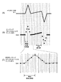
図10(A)はサンプリングポイントとAPD出力S2の波形とを示す図であり、図10(B)はサンプリングジッタに起因するサンプル波形と平均波形との波形のズレを示す図である。図10(A)に示すように、APD出力波形S2に対して、サンプリングポイントがAおよびBのようにずれた場合、特にサンプル波形S3のレベルが非常に大きく時間変化する部分では信号レベルが大きく変化することが分かる。 FIG. 10A is a diagram showing the sampling point and the waveform of the APD output S2, and FIG. 10B is a diagram showing the waveform deviation between the sample waveform and the average waveform due to sampling jitter. As shown in FIG. 10A, when the sampling points are shifted as A and B with respect to the APD output waveform S2, the signal level is large especially in the portion where the level of the sample waveform S3 is very large and changes with time. You can see that it changes.
図10(B)に示すように、白丸で示す平均波形S4に対して、サンプル波形S3のサンプリングポイントがずれて黒丸で示す波形S3となった場合、光子検出を識別する識別窓での信号レベルが変動する。このためにサンプル波形S3と平均波形S4との比較により信号識別を行うと、ジッタによる波形の差を誤識別する可能性がある。 As shown in FIG. 10B, when the sampling point of the sample waveform S3 is shifted to the waveform S3 indicated by a black circle with respect to the average waveform S4 indicated by a white circle, the signal level in the identification window for identifying photon detection Fluctuates. For this reason, if signal identification is performed by comparing the sample waveform S3 and the average waveform S4, there is a possibility that a waveform difference due to jitter may be erroneously identified.
そこで、本発明の目的は、サンプリングクロックがジッタを持っていても、精度の良い識別が可能な光子検出回路および光子検出方法を提供することにある。 SUMMARY OF THE INVENTION An object of the present invention is to provide a photon detection circuit and a photon detection method capable of accurately discriminating even when a sampling clock has jitter.
本発明による光子検出回路は、受光素子に所定周期でゲートパルスを印加することにより光子検出を行う光子検出回路であって、前記受光素子の前記所定周期単位のサンプル波形データを平均することで平均波形データを生成するゲート周期平均化手段と、前記平均波形データと前記受光素子から出力されたサンプル波形データとの位相差をなくすように、前記平均波形データおよび前記出力されたサンプル波形データの少なくとも一方の位相を調整する位相調整手段と、位相調整された前記平均波形データに対する前記出力されたサンプル波形データから光子検出の識別を行う識別手段と、を有することを特徴とする。 A photon detection circuit according to the present invention is a photon detection circuit that performs photon detection by applying a gate pulse to a light receiving element at a predetermined period, and averages the sample waveform data of the predetermined period unit of the light receiving element. Gate period averaging means for generating waveform data; and at least the average waveform data and the output sample waveform data so as to eliminate a phase difference between the average waveform data and the sample waveform data output from the light receiving element. Phase adjustment means for adjusting one phase and identification means for identifying photon detection from the output sample waveform data with respect to the phase-adjusted average waveform data.
本発明によれば、サンプリングクロックがジッタを持っていても、光子検出の精度の良い識別が可能となる。 According to the present invention, it is possible to identify photons with high accuracy even if the sampling clock has jitter.
1.一実施形態
図1は本発明の一実施形態による光子検出回路の概略的な構成を示すブロック図である。ここでは、ゲートパルス駆動によって光子検出可能な受光素子としてアバランシェ・フォトダイオード(APD)を用いた光子検出回路を例示する。
1. FIG. 1 is a block diagram showing a schematic configuration of a photon detection circuit according to an embodiment of the present invention. Here, a photon detection circuit using an avalanche photodiode (APD) as a light receiving element capable of detecting photons by gate pulse driving is illustrated.
APD10にはゲート生成回路11からゲートパルスS20が所定周期(ゲート周期)で印加される。ゲート生成回路11はゲートクロックCLKgに従ってゲートパルスS20をゲート周期で生成する。これによってAPD10はゲートパルスS20の微分波形を含むAPD出力S21をゲート周期で出力する。ゲートパルスS20が印加されている期間に光子信号S1が入射すると、これによって、ゲートパルスS20の微分波形に光子に起因する受光成分が重畳されたAPD出力S21が出力される。
A gate pulse S20 is applied to the
APD出力S21は、サンプリング部12によってサンプリングクロックCLKsに従ってサンプリングされ、サンプリングされた離散的な時系列データS22(以下、サンプル波形S22という。)としてゲート周期波形平均化部13へ出力される。ゲート周期波形平均化部13は、ゲートクロックCLKgおよびサンプリングクロックCLKsを入力し、ゲート周期ごとのサンプル波形S22を各時点で平均化し、その平均化された時系列データS23(以下、平均波形S23という。)を位相調整部へ出力する。
The APD output S21 is sampled by the
位相調整部は位相差検出部14および位相シフト部15からなる。位相差検出部14は、サンプル波形S22と平均波形S23とを後述する位相比較窓の期間で比較することにより位相差を検出し、その位相差信号S24を位相シフト部15へ出力する。
The phase adjustment unit includes a phase
位相シフト部15は、位相差をゼロにするように、サンプル波形S22あるいは平均波形S23を相対的に位相シフトさせ、位相が合致したサンプル波形S22cおよび平均波形S23cを識別部16へ出力する。
The
識別部16は、平均波形S23cに対するサンプル波形S22cの差分を識別窓の期間で検出し、その差分と所定閾値との比較結果を光子検出信号S25として出力する。
The
上述したように、光子信号S1の光子到達率が低い場合には、平均波形S23は実質的にゲートパルスS20の微分波形に近い波形となる。したがって、識別部16は平均波形S23cに対するサンプル波形S22cの差分からチャージパルス補償された光子検出信号S25を得ることができる。
As described above, when the photon arrival rate of the photon signal S1 is low, the average waveform S23 is a waveform substantially close to the differential waveform of the gate pulse S20. Therefore, the
さらに、本実施形態によれば、識別部16には、位相が合致したサンプル波形S22cおよび平均波形S23cが入力するので、サンプリングクロックCLKsのジッタによりサンプリング部12でサンプリングポイントのズレが発生しても、正確な光子検出を行うことができる。言い換えれば、サンプル波形S22cと平均波形S23cとの比較によりサンプリングクロックCLKsのジッタを推測し、信号識別の精度劣化を回避することができる。
Furthermore, according to the present embodiment, since the sample waveform S22c and the average waveform S23c having the same phase are input to the
なお、サンプリング部12、ゲート周期波形平均化部13、位相差検出部14、位相シフト部15および識別部16と同等の機能は、プログラムをCPU等のプログラム制御プロセッサ上で実行することにより実現することもできる。
The functions equivalent to those of the
2.第1実施例
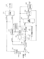
2.1)構成
図2は本発明の第1実施例による光子検出回路の構成を示すブロック図である。APD101には直流バイアス電圧に重畳してゲート生成回路102からゲートパルスS20が所定周期(ゲート周期)で印加される。ゲート生成回路102は、ゲートクロックCLKgに従って、APD101のブレークダウン電圧(VBd)以上の逆バイアス電圧(ゲートパルスS20)をゲート周期で生成する。これによってAPD101はゲートパルスS20の微分波形を含むAPD出力S21をゲート周期で出力する。上述したように、ゲートパルスS20が印加されている期間に光子信号S1が入射すると、ゲートパルスS20の微分波形に光子に起因する受光成分が重畳されたAPD出力S21が出力される。
2. First Embodiment 2.1) Configuration FIG. 2 is a block diagram showing a configuration of a photon detection circuit according to a first embodiment of the present invention. A gate pulse S20 is applied to the
APD出力S21はサンプリング部103によってサンプリングクロックCLKsに従ってサンプリングされ、離散的なサンプル波形S22としてゲート周期波形平均化部へ出力される。ゲート周期波形平均化部は、メモリ104、波形平均化部105およびメモリ制御部106からなる。サンプル波形S22はメモリ104に蓄積され、波形平均化部105によって平均波形S23が生成される。
The APD output S21 is sampled by the
具体的には、メモリ制御部106のアドレス制御によりサンプル波形S22はメモリ104に時系列に書き込まれ、波形平均化部105はその時系列のサンプル波形S22をゲート周期単位で読み出してゲート周期内の各サンプリングポイントでの平均レベルを算出し、ゲート周期における平均波形S23を生成する。
Specifically, the sample waveform S22 is written to the
こうして生成された平均波形S23は位相調整部107に入力し、サンプル波形S22と位相調整される。位相調整部107は、上述した位相差検出部14および位相シフト部15により構成することができるが、本実施例では、平均波形S23だけを位相シフトさせてサンプル波形S22の位相と合致させている。
The average waveform S23 generated in this way is input to the
位相調整された平均波形S23cは補間部108に入力する。補間部108は平均波形S23cから後述する補償平均波形S30を生成して識別部109へ出力する。識別部109は、ゲートクロックCLKgに従ってサンプル波形S22と補償平均波形S30を入力し、2つの波形の差分を演算することで光子検出信号の有無を識別し光子検出信号S31を生成する。
The phase-adjusted average waveform S23c is input to the
なお、クロック源110およびクロック処理部111によってゲートクロックCLKgおよびサンプリングクロックCLKsが生成される。ゲートクロックCLKgはゲート生成部102、メモリ制御部106および識別部109へ出力され、サンプリングクロックCLKsはサンプリング部103およびメモリ制御部106に出力される。
The
2.2)位相調整および補間動作
次に、本実施例による光子検出回路の位相調整部107および補間部108による補償平均波形S30の生成動作について説明する。
2.2) Phase Adjustment and Interpolation Operation Next, the generation operation of the compensated average waveform S30 by the
図3(A)はサンプリングポイントとAPD出力S21の波形とを示す図であり、図3(B)はサンプリングジッタ等に起因するサンプル波形と平均波形との波形のズレと位相検出動作を説明するための図であり、図3(C)は位相調整されたサンプル波形および平均波形と保管された平均波形を示す図である。 FIG. 3A is a diagram showing the sampling points and the waveform of the APD output S21, and FIG. 3B is a diagram for explaining the waveform shift and phase detection operation between the sample waveform and the average waveform caused by sampling jitter and the like. FIG. 3C is a diagram showing the sample waveform and the average waveform that are phase-adjusted and the stored average waveform.
ここでは図3(A)に示すAPD出力波形S21に対してサンプリングポイントがずれた場合を考える。この場合、図3(B)に示すように、白丸で示す平均波形S23に対して、サンプル波形S22は黒丸で示すように位相がシフトしている。 Here, consider a case where the sampling point is deviated from the APD output waveform S21 shown in FIG. In this case, as shown in FIG. 3B, the phase of the sample waveform S22 is shifted as indicated by a black circle with respect to the average waveform S23 indicated by a white circle.
既に述べたように、APD101に光子が入射して電流が流れた場合、識別窓Wdで示した領域に受光成分が出現する。したがって、ゲートパルス立ち上がり部分のチャージパルスでは、サンプル波形S22と平均波形S23とは本体同じ値を取るべきであるが、サンプリングポイントがずれたことにより、図3(B)に示す白丸と黒丸のように波形に差が生じている。
As already described, when a photon is incident on the
そこで、本実施例では、ゲートパルスの立ち上がり部分に対応するチャージパルスに対して位相比較窓Wphを設定し、位相差検出部14が位相比較窓Wphの範囲内で2つの波形S22およびS23の位相差信号S24を算出する。例えば、平均波形S23の近似波形201を算出し、サンプル波形S22との時間差を算出することで、位相差を求める事が可能である。ここでは近似波形201は、位相比較窓Wphの範囲での平均波形S23を直線近似した例を示している。位相シフト部15は、位相差信号S24で示す位相差だけ平均波形S23をシフトさせて平均波形S23cを生成し補間部108へ出力する。
Therefore, in the present embodiment, the phase comparison window Wph is set for the charge pulse corresponding to the rising portion of the gate pulse, and the phase
補間部108は位相調整された平均波形S23cのサンプル値間を補間することで、補償平均波形S30を生成して識別部109へ出力する。補償平均波形S30はサンプリングクロックCLKsのジッタを補償した平均波形となるので、この補償平均波形S30とサンプル波形S22とは図3(C)に示すように重なり、識別窓Wdの範囲の誤差が補償され、その結果誤検出が回避可能となる。
The
2.3)効果
本発明の第1実施例によれば、サンプル波形S22と平均波形S23cとの位相を合致させ、さらに平均波形S23cを補間したもので光子検出の識別を行っているので、サンプリングクロックCLKsのジッタによりサンプリング部12でサンプリングポイントのズレが発生しても、識別部109において正確な光子検出を行うことができる。
2.3) Effect According to the first embodiment of the present invention, the phase of the sample waveform S22 and the average waveform S23c are matched, and the average waveform S23c is interpolated to identify photon detection. Even if a sampling point shift occurs in the
3.第2実施例
上述した第1実施例による光子検出回路において、サンプリング部103のサンプリング周期を密にすることでサンプル波形の補間精度更に向上させることができる。本発明の第2実施例による光子検出回路では、平均波形の補間精度の向上を目的として、メモリに格納するサンプル波形の間隔を密にする機能が付加される。
3. Second Embodiment In the photon detection circuit according to the first embodiment described above, the interpolation accuracy of the sample waveform can be further improved by making the sampling period of the
図4は本発明の第2実施例による光子検出回路の構成を示すブロック図である。ただし、図2に示す第1実施例の回路と同じ機能を有するブロックには同一参照番号を付して詳細な説明は省略する。 FIG. 4 is a block diagram showing the configuration of the photon detection circuit according to the second embodiment of the present invention. However, the blocks having the same functions as those of the circuit of the first embodiment shown in FIG.
本実施例では、サンプリングクロックCLKsが可変遅延部120を通してサンプリングクロックCLKs+としてサンプリング部103およびメモリ制御部106へそれぞれ供給される。可変遅延部120の遅延量は遅延制御部121からの遅延制御信号S40により制御され、サンプリングクロックCLKsの位相を少なくとも2π以下の幅で変化させる。これにより、サンプリングの時間分解能を向上させることができる。
In this embodiment, the sampling clock CLKs is supplied to the
また、遅延制御部121からの遅延制御信号S40はメモリ制御部106にも供給され、メモリ104のメモリアドレスに関して遅延量を反映した制御が可能となる。すなわち、メモリ制御回路106は、遅延量の調整ステップ数に対応する大きなメモリアドレス空間の制御を行う。
Further, the delay control signal S40 from the
可変遅延部120からのサンプリングクロックCLKs+に従って、サンプリング部103は、APD出力S21をサンプリングし、サンプル波形S41を生成する。このサンプル波形S41は、サンプリングクロックCLKs+の周期に相当する時間分解能を持つ。本実施例では、光子検出シーケンスを実行する前に、平均波形S42を高精度に生成するトレーニングシーケンスを定義し、その間に可変遅延部120を動作させることができる。
In accordance with the sampling clock CLKs + from the
一例として、可変遅延部120の遅延量を0、π/2、π、3π/2の4段階で制御を行う場合について説明する。
As an example, a case will be described in which the delay amount of the
図5(A)はAPD出力S21の波形を示す図であり、図5(B)はサンプリングクロックCLKsにより得られるサンプル波形S22を示す図であり、図5(C)はサンプリングクロックCLKs+により得られるサンプル波形S41における位相比較窓の前後の部分(チャージパルス部分)を示す拡大図である。 5A is a diagram showing a waveform of the APD output S21, FIG. 5B is a diagram showing a sample waveform S22 obtained by the sampling clock CLKs, and FIG. 5C is obtained by the sampling clock CLKs +. It is an enlarged view showing a portion (charge pulse portion) before and after the phase comparison window in sample waveform S41.
本実施例では、可変遅延部120の遅延量が0、π/2、π、3π/2の4段階で制御されるので、図5(C)の白丸で示すように4倍の時間分解能でAPD出力S21のサンプリングを行い、メモリ104にサンプル波形S41を格納する。メモリ104は、分解能の向上、つまり、可変遅延部120の可変ステップ数に相当するだけの容量を備える必要がある。この場合、4段階の遅延制御ステップであれば、図2におけるメモリ104のメモリ量に対して、4倍のメモリ量を備える。
In this embodiment, since the delay amount of the
このように、本実施例によれば、サンプリングクロックCLKsを可変遅延制御によりスキャンし、それに対応するようにメモリ104の容量を拡張することにより、生成する平均波形S42の時間分解能を向上させることができる。これにより位相調整部107での位相比較処理の精度が改善される。すなわち、チャージパルスの時間幅に対してサンプリングクロックCLKsの周期が広い場合であっても、位相比較の精度劣化を回避することができる。
As described above, according to the present embodiment, the sampling clock CLKs is scanned by the variable delay control, and the capacity of the
4.第3実施例
上述した第2実施例による光子検出回路では、サンプリング部103のサンプリング周期を密にすることでサンプル波形の補間精度更に向上させることができるが、本発明の第3実施例による光子検出回路では、サンプリングの時間分解能を十分に向上させる事により補間処理を省略することが可能である。
4). Third Embodiment In the photon detection circuit according to the second embodiment described above, it is possible to further improve the interpolation accuracy of the sample waveform by making the sampling period of the
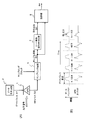
図6は本発明の第3実施例による光子検出回路の構成を示すブロック図である。ただし、図4に示す第2実施例の回路と同じ機能を有するブロックには同一参照番号を付して詳細な説明は省略する。本実施例によれば、位相調整部107の位相調整後の平均波形S42cは、セレクタ130により選択平均波形S50として識別部131へ出力される。
FIG. 6 is a block diagram showing the configuration of the photon detection circuit according to the third embodiment of the present invention. However, the blocks having the same functions as those of the circuit of the second embodiment shown in FIG. According to the present embodiment, the average waveform S42c after the phase adjustment by the
たとえば、上述したように可変遅延部120の遅延量を0、π/2、π、3π/2の4段階で制御することで、4倍の分解能の向上が得られたが、更に微細に遅延制御を行う事で平均波形S42の誤差を減少させることができる。したがって、可変遅延部120の遅延ステップ数を増大させることにより、補間処理を必要としない程に十分な精度を持つ平均波形S42cとして生成する事が可能となる。この場合、識別部131で必要とするデータ量は平均波形S42cのように多量ではないので、セレクタ130によって平均波形S42cから識別窓Wdの処理を行うのに必要十分な選択平均波形S50を生成して識別部131へ出力する。言い換えれば、ゲート周期のうち、識別窓に対応するタイミングの平均波形S42cのみを選択平均波形S50として識別部131へ出力すればよい。
For example, as described above, by controlling the delay amount of the
このように、可変遅延部120の遅延制御ステップ数を増大させることで補間処理を省略することが可能な程度に十分な精度をもつ平均波形S42を生成することができる。サンプリング精度を高めることでメモリ104の容量は増大するが、第1実施例のような補間部108を省略することができ、処理回路の規模の削減と同時に、補間処理に必要な演算時間の圧縮が可能となる。
Thus, by increasing the number of delay control steps of the
5.第4実施例
上述した第3実施例では、補間処理を省略することができる反面、メモリ104の容量が増大する。そこで、本発明の第4実施例では、補間処理を省略し、かつメモリ104の容量を削減可能な構成を提供する。
5. Fourth Embodiment In the third embodiment described above, the interpolation process can be omitted, but the capacity of the
図7は本発明の第4実施例による光子検出回路の構成を示すブロック図である。ただし、図6に示す第3実施例の回路と同じ機能を有するブロックには同一参照番号を付して詳細な説明は省略する。本実施例によれば、ゲート周期波形平均化部のメモリ104の前段にスイッチ140を設けることで、メモリ104の容量の増大を回避する。
FIG. 7 is a block diagram showing the configuration of the photon detection circuit according to the fourth embodiment of the present invention. However, the blocks having the same functions as those of the circuit of the third embodiment shown in FIG. According to the present embodiment, an increase in the capacity of the
スイッチ140は、メモリ制御部106の制御によりサンプル波形S41をメモリ104へ選択的に伝達する。すなわち、サンプル波形S41の識別処理に必要となる部分は、位相比較窓および識別窓の時間領域のみであるから、スイッチ140は、サンプル波形S41の必要な位相部分のみを選択的にメモリ104に格納する。これによってメモリ104の容量の増大を回避することができる。具体体な動作例を次に説明する。
The
図8(A)はAPD出力S21の波形を示す図であり、図8(B)はサンプリングクロックCLKs+により得られるサンプル波形S41を示す図であり、図8(C)は位相比較窓および識別窓を選択するスイッチタイミング信号を示す波形図である。 8A shows a waveform of the APD output S21, FIG. 8B shows a sample waveform S41 obtained by the sampling clock CLKs +, and FIG. 8C shows a phase comparison window and an identification window. It is a wave form diagram which shows the switch timing signal which selects.
上述したようにサンプル波形S41の識別処理に必要となる部分は、位相比較窓および識別窓の時間領域のみであるから、図8(C)に示すように、位相比較窓および識別窓に対応するタイムスロットのみ、サンプル波形S41をメモリ104に伝達するようにスイッチ140を制御すればよい。たとえば、図8(C)に示すような波形のスイッチ制御信号をメモリ制御部106がスイッチ140へ出力し、位相比較窓および識別窓のタイミングでサンプル波形S41をメモリ104へ通過させ、その他の期間ではサンプル波形S41をメモリ104に格納されない。
As described above, the part necessary for the identification processing of the sample waveform S41 is only the time region of the phase comparison window and the identification window, and therefore corresponds to the phase comparison window and the identification window as shown in FIG. It is only necessary to control the
このようにメモリ制御を行うことで、サンプリングの時間分解能を十分に向上させることで補間処理を省略することができ、かつメモリ104の容量を削減することが可能となる。
By performing memory control in this way, interpolation processing can be omitted by sufficiently improving the sampling time resolution, and the capacity of the
本発明による光子検出回路は、量子鍵配信装置および量子暗号装置、あるいは、光子数検出器、Optical Time Domain Reflectmeter (OTDR)、分光器、暗視野カメラなどの光子検出部に適用することができる。 The photon detection circuit according to the present invention can be applied to a quantum key distribution device and a quantum encryption device, or a photon detection unit such as a photon number detector, an optical time domain reflectometer (OTDR), a spectroscope, and a dark field camera.
10 アバランシェ・フォトダイオード(APD)
11 ゲート生成部
12 サンプリング部
13 ゲート周期波形平均化部
14 位相差検出部
15 位相シフト部
16 識別部
CLKg ゲートクロック
CLKs サンプリングクロック
S20 ゲートパルス
S21 APD出力
S22 サンプル波形
S23 平均波形
S22c 位相調整後のサンプル波形
S23c 位相調整後の平均波形
S24 位相差信号
S25 光子検出信号
10 Avalanche photodiode (APD)
Claims (17)
前記受光素子の前記所定周期単位のサンプル波形データを平均することで平均波形データを生成するゲート周期平均化手段と、
前記平均波形データと前記受光素子から出力されたサンプル波形データとの位相差をなくすように、前記平均波形データおよび前記出力されたサンプル波形データの少なくとも一方の位相を調整する位相調整手段と、
位相調整された前記平均波形データに対する前記出力されたサンプル波形データから光子検出の識別を行う識別手段と、
を有することを特徴とする光子検出回路。 In a photon detection circuit that performs photon detection by applying a gate pulse to a light receiving element at a predetermined period,
Gate period averaging means for generating average waveform data by averaging the sample waveform data of the predetermined period unit of the light receiving element;
Phase adjusting means for adjusting a phase of at least one of the average waveform data and the output sample waveform data so as to eliminate a phase difference between the average waveform data and the sample waveform data output from the light receiving element;
An identification means for identifying photon detection from the output sample waveform data with respect to the averaged waveform data adjusted in phase;
A photon detection circuit comprising:
前記スキャンされたサンプリングクロックにより得られた前記所定周期ごとの稠密なサンプル波形データを格納する格納手段と、
を有し、前記ゲート周期平均化手段は前記格納手段に格納された前記稠密なサンプル波形データを前記所定周期単位のサンプル波形データとして入力することを特徴とする請求項1−5のいずれか1項に記載の光子検出回路。 Variable delay means for scanning the phase of a sampling clock at a predetermined step when obtaining the sample waveform data by sampling the output waveform of the light receiving element;
Storage means for storing dense sample waveform data for each predetermined period obtained by the scanned sampling clock;
The gate period averaging means inputs the dense sample waveform data stored in the storage means as the sample waveform data of the predetermined period unit. The photon detection circuit according to item.
前記受光素子の前記所定周期単位のサンプル波形データを平均することで平均波形データを生成し、
前記平均波形データと前記受光素子から出力されたサンプル波形データとの位相差をなくすように、前記平均波形データおよび前記出力されたサンプル波形データの少なくとも一方の位相を調整し、
位相調整された前記平均波形データに対する前記出力されたサンプル波形データから光子検出の識別を行う、
ことを特徴とする光子検出方法。 In a photon detection method for performing photon detection by applying a gate pulse to a light receiving element at a predetermined period,
The average waveform data is generated by averaging the sample waveform data of the predetermined period unit of the light receiving element,
Adjusting the phase of at least one of the average waveform data and the output sample waveform data so as to eliminate a phase difference between the average waveform data and the sample waveform data output from the light receiving element;
Identifying photon detection from the output sample waveform data relative to the phase adjusted average waveform data;
The photon detection method characterized by the above-mentioned.
前記補間された平均波形データに対する前記出力されたサンプル波形データから光子検出の識別を行うことを特徴とする請求項9−12のいずれか1項に記載の光子検出方法。 Interpolate the phase adjusted average waveform data,
The photon detection method according to claim 9, wherein photon detection is identified from the output sample waveform data with respect to the interpolated average waveform data.
前記スキャンされたサンプリングクロックにより得られた前記所定周期ごとの稠密なサンプル波形データを格納手段に格納し、
前記格納手段に格納された前記稠密なサンプル波形データを前記所定周期単位のサンプル波形データとして平均化することを特徴とする請求項9−13のいずれか1項に記載の光子検出方法。 The sampling clock phase when obtaining the sample waveform data by sampling the output waveform of the light receiving element is scanned in a predetermined step,
Storing dense sample waveform data for each predetermined period obtained by the scanned sampling clock in a storage means;
The photon detection method according to any one of claims 9 to 13, wherein the dense sample waveform data stored in the storage means is averaged as the sample waveform data of the predetermined period unit.
前記受光素子の前記所定周期単位のサンプル波形データを平均することで平均波形データを生成するゲート周期平均化手段と、
前記平均波形データと前記受光素子から出力されたサンプル波形データとの位相差をなくすように、前記平均波形データおよび前記出力されたサンプル波形データの少なくとも一方の位相を調整する位相調整手段と、
位相調整された前記平均波形データに対する前記出力されたサンプル波形データから光子検出の識別を行う識別手段と、
として前記コンピュータを機能させるプログラム。 In a program for causing a computer to function as a photon detection circuit that performs photon detection by applying a gate pulse to a light receiving element at a predetermined period,
Gate period averaging means for generating average waveform data by averaging the sample waveform data of the predetermined period unit of the light receiving element;
Phase adjusting means for adjusting a phase of at least one of the average waveform data and the output sample waveform data so as to eliminate a phase difference between the average waveform data and the sample waveform data output from the light receiving element;
An identification means for identifying photon detection from the output sample waveform data with respect to the averaged waveform data adjusted in phase;
A program for causing the computer to function as
Priority Applications (3)
| Application Number | Priority Date | Filing Date | Title |
|---|---|---|---|
| JP2008074894A JP2009229247A (en) | 2008-03-24 | 2008-03-24 | Photon detector having phase adjustment function and photon detection method |
| US12/409,323 US20090236501A1 (en) | 2008-03-24 | 2009-03-23 | Photon detection method and circuit having phase adjuster |
| CN200910129361A CN101545811A (en) | 2008-03-24 | 2009-03-24 | Photon detection method and circuit having phase adjuster |
Applications Claiming Priority (1)
| Application Number | Priority Date | Filing Date | Title |
|---|---|---|---|
| JP2008074894A JP2009229247A (en) | 2008-03-24 | 2008-03-24 | Photon detector having phase adjustment function and photon detection method |
Publications (1)
| Publication Number | Publication Date |
|---|---|
| JP2009229247A true JP2009229247A (en) | 2009-10-08 |
Family
ID=41087930
Family Applications (1)
| Application Number | Title | Priority Date | Filing Date |
|---|---|---|---|
| JP2008074894A Withdrawn JP2009229247A (en) | 2008-03-24 | 2008-03-24 | Photon detector having phase adjustment function and photon detection method |
Country Status (3)
| Country | Link |
|---|---|
| US (1) | US20090236501A1 (en) |
| JP (1) | JP2009229247A (en) |
| CN (1) | CN101545811A (en) |
Cited By (3)
| Publication number | Priority date | Publication date | Assignee | Title |
|---|---|---|---|---|
| JP2014131259A (en) * | 2012-10-12 | 2014-07-10 | Toshiba Corp | System and method for intensity monitoring |
| WO2015178400A1 (en) * | 2014-05-22 | 2015-11-26 | 株式会社ユニソク | Transient absorption measurement method and transient absorption measurement device |
| JP2018164029A (en) * | 2017-03-27 | 2018-10-18 | 株式会社デンソー | Photodetector |
Families Citing this family (12)
| Publication number | Priority date | Publication date | Assignee | Title |
|---|---|---|---|---|
| US8766161B2 (en) * | 2009-12-02 | 2014-07-01 | Nucript LLC | System for controling and calibrating single photon detection devices |
| US10069619B1 (en) * | 2011-08-05 | 2018-09-04 | Rockwell Collins, Inc. | Optical sample and hold system and method |
| US9197471B1 (en) | 2011-08-05 | 2015-11-24 | Rockwell Collins, Inc. | Optically interleaved photonic analog to digital converters |
| US9596421B1 (en) * | 2013-01-17 | 2017-03-14 | Princeton Lightwave, Inc. | Apparatus comprising a high dynamic range single-photon passive 2d imager and methods therefor |
| US9356704B1 (en) * | 2013-08-09 | 2016-05-31 | Rockwell Collins, Inc. | Optical conversion system and method with multiple phase processing |
| US9118423B1 (en) | 2013-08-09 | 2015-08-25 | Rockwell Collins.com | Optical conversion system and method with multiple amplitude processing |
| CN103528695B (en) * | 2013-10-14 | 2016-03-09 | 中国人民解放军理工大学 | Sampling single-photon detector and adaptive differential decision method thereof |
| CN105136317B (en) * | 2015-09-10 | 2018-06-29 | 中国人民解放军理工大学 | Single-point sampling judgement single-photon detector and its sampling decision method |
| US9671284B1 (en) * | 2016-01-14 | 2017-06-06 | Kiskeya Microsystems Llc | Single-photon avalanche diode circuit with variable hold-off time and dual delay regime |
| CN107843350B (en) * | 2017-12-11 | 2019-06-07 | 中国人民解放军国防科技大学 | Frequency-adjustable high-speed near-infrared single photon detector based on sampling |
| JP7324050B2 (en) * | 2019-05-27 | 2023-08-09 | 株式会社東芝 | Waveform segmentation device and waveform segmentation method |
| CN112414567B (en) * | 2021-01-21 | 2021-04-20 | 浙江九州量子信息技术股份有限公司 | APD digital avalanche signal extraction system with synchronous correlated sampling |
Family Cites Families (2)
| Publication number | Priority date | Publication date | Assignee | Title |
|---|---|---|---|---|
| US20040093388A1 (en) * | 2002-11-13 | 2004-05-13 | Chandler James E. | Test validation of an integrated device |
| JP4716004B2 (en) * | 2005-03-31 | 2011-07-06 | 日本電気株式会社 | Photon detection circuit and noise elimination method |
-
2008
- 2008-03-24 JP JP2008074894A patent/JP2009229247A/en not_active Withdrawn
-
2009
- 2009-03-23 US US12/409,323 patent/US20090236501A1/en not_active Abandoned
- 2009-03-24 CN CN200910129361A patent/CN101545811A/en active Pending
Cited By (7)
| Publication number | Priority date | Publication date | Assignee | Title |
|---|---|---|---|---|
| JP2014131259A (en) * | 2012-10-12 | 2014-07-10 | Toshiba Corp | System and method for intensity monitoring |
| WO2015178400A1 (en) * | 2014-05-22 | 2015-11-26 | 株式会社ユニソク | Transient absorption measurement method and transient absorption measurement device |
| JP2015222192A (en) * | 2014-05-22 | 2015-12-10 | 株式会社ユニソク | Transient absorption measuring method and transient absorption measuring device |
| US9709497B2 (en) | 2014-05-22 | 2017-07-18 | Unisoku Co., Ltd. | Transient absorption measurement method and transient absorption measurement apparatus |
| JP2018164029A (en) * | 2017-03-27 | 2018-10-18 | 株式会社デンソー | Photodetector |
| CN110462846A (en) * | 2017-03-27 | 2019-11-15 | 株式会社电装 | Photodetector |
| CN110462846B (en) * | 2017-03-27 | 2022-08-05 | 株式会社电装 | Light detector |
Also Published As
| Publication number | Publication date |
|---|---|
| US20090236501A1 (en) | 2009-09-24 |
| CN101545811A (en) | 2009-09-30 |
Similar Documents
| Publication | Publication Date | Title |
|---|---|---|
| JP2009229247A (en) | Photon detector having phase adjustment function and photon detection method | |
| US8766161B2 (en) | System for controling and calibrating single photon detection devices | |
| US10185032B2 (en) | Time measurement circuit and optoelectronic distance meter having such a time measurement circuit | |
| JP4716004B2 (en) | Photon detection circuit and noise elimination method | |
| US7945408B2 (en) | Time delay estimation | |
| EP1752793B1 (en) | Method and device for redundant distance measurement and mismatch cancellation in phase-measurement systems | |
| US20150041625A1 (en) | Time to digital converter and applications thereof | |
| JP4952461B2 (en) | Random number generation apparatus and random number generation method | |
| EP2365291B1 (en) | Photoelectric encoder | |
| JP2010504694A (en) | Optical signal field restoration and repair | |
| US20140292311A1 (en) | Position detector | |
| JP4907647B2 (en) | Waveform shaping device and error measuring device | |
| JP6838532B2 (en) | Sensor device and measurement method | |
| CN101188058A (en) | Data collection system and method based on multi-digital path and intercrossed calibration | |
| JP5042701B2 (en) | Optical sampling apparatus and optical sampling method | |
| JP2007208805A (en) | Imaging apparatus and image sensor | |
| JP5446094B2 (en) | Photon detection device, photon detection method, and photon detection program | |
| JP6760612B2 (en) | Phase measuring device and equipment to which this phase measuring device is applied | |
| JP2007036513A (en) | Photon receiver and method for receiving photon | |
| JP4489790B2 (en) | Optical phase modulation evaluation apparatus and calibration method thereof | |
| CN111665521A (en) | Derivation of depth information from time-of-flight (TOF) sensor data | |
| JPWO2016076419A1 (en) | Phase measuring device and equipment to which the phase measuring device is applied | |
| Nicola et al. | A SPAD-based random number generator pixel based on the arrival time of photons | |
| US10797707B2 (en) | Delay locked loop detection method and system | |
| JP2019016900A (en) | Method and apparatus for timing adjustment of photon detector |
Legal Events
| Date | Code | Title | Description |
|---|---|---|---|
| A300 | Application deemed to be withdrawn because no request for examination was validly filed |
Free format text: JAPANESE INTERMEDIATE CODE: A300 Effective date: 20110607 |