JP2009223070A - ドライバicおよび有機elパネル - Google Patents
ドライバicおよび有機elパネル Download PDFInfo
- Publication number
- JP2009223070A JP2009223070A JP2008068632A JP2008068632A JP2009223070A JP 2009223070 A JP2009223070 A JP 2009223070A JP 2008068632 A JP2008068632 A JP 2008068632A JP 2008068632 A JP2008068632 A JP 2008068632A JP 2009223070 A JP2009223070 A JP 2009223070A
- Authority
- JP
- Japan
- Prior art keywords
- memory
- correction
- display
- data
- driver
- Prior art date
- Legal status (The legal status is an assumption and is not a legal conclusion. Google has not performed a legal analysis and makes no representation as to the accuracy of the status listed.)
- Pending
Links
Images


Classifications
-
- G—PHYSICS
- G09—EDUCATION; CRYPTOGRAPHY; DISPLAY; ADVERTISING; SEALS
- G09G—ARRANGEMENTS OR CIRCUITS FOR CONTROL OF INDICATING DEVICES USING STATIC MEANS TO PRESENT VARIABLE INFORMATION
- G09G3/00—Control arrangements or circuits, of interest only in connection with visual indicators other than cathode-ray tubes
- G09G3/20—Control arrangements or circuits, of interest only in connection with visual indicators other than cathode-ray tubes for presentation of an assembly of a number of characters, e.g. a page, by composing the assembly by combination of individual elements arranged in a matrix no fixed position being assigned to or needed to be assigned to the individual characters or partial characters
- G09G3/22—Control arrangements or circuits, of interest only in connection with visual indicators other than cathode-ray tubes for presentation of an assembly of a number of characters, e.g. a page, by composing the assembly by combination of individual elements arranged in a matrix no fixed position being assigned to or needed to be assigned to the individual characters or partial characters using controlled light sources
- G09G3/30—Control arrangements or circuits, of interest only in connection with visual indicators other than cathode-ray tubes for presentation of an assembly of a number of characters, e.g. a page, by composing the assembly by combination of individual elements arranged in a matrix no fixed position being assigned to or needed to be assigned to the individual characters or partial characters using controlled light sources using electroluminescent panels
- G09G3/32—Control arrangements or circuits, of interest only in connection with visual indicators other than cathode-ray tubes for presentation of an assembly of a number of characters, e.g. a page, by composing the assembly by combination of individual elements arranged in a matrix no fixed position being assigned to or needed to be assigned to the individual characters or partial characters using controlled light sources using electroluminescent panels semiconductive, e.g. using light-emitting diodes [LED]
- G09G3/3208—Control arrangements or circuits, of interest only in connection with visual indicators other than cathode-ray tubes for presentation of an assembly of a number of characters, e.g. a page, by composing the assembly by combination of individual elements arranged in a matrix no fixed position being assigned to or needed to be assigned to the individual characters or partial characters using controlled light sources using electroluminescent panels semiconductive, e.g. using light-emitting diodes [LED] organic, e.g. using organic light-emitting diodes [OLED]
- G09G3/3225—Control arrangements or circuits, of interest only in connection with visual indicators other than cathode-ray tubes for presentation of an assembly of a number of characters, e.g. a page, by composing the assembly by combination of individual elements arranged in a matrix no fixed position being assigned to or needed to be assigned to the individual characters or partial characters using controlled light sources using electroluminescent panels semiconductive, e.g. using light-emitting diodes [LED] organic, e.g. using organic light-emitting diodes [OLED] using an active matrix
- G09G3/3233—Control arrangements or circuits, of interest only in connection with visual indicators other than cathode-ray tubes for presentation of an assembly of a number of characters, e.g. a page, by composing the assembly by combination of individual elements arranged in a matrix no fixed position being assigned to or needed to be assigned to the individual characters or partial characters using controlled light sources using electroluminescent panels semiconductive, e.g. using light-emitting diodes [LED] organic, e.g. using organic light-emitting diodes [OLED] using an active matrix with pixel circuitry controlling the current through the light-emitting element
-
- G—PHYSICS
- G09—EDUCATION; CRYPTOGRAPHY; DISPLAY; ADVERTISING; SEALS
- G09G—ARRANGEMENTS OR CIRCUITS FOR CONTROL OF INDICATING DEVICES USING STATIC MEANS TO PRESENT VARIABLE INFORMATION
- G09G2300/00—Aspects of the constitution of display devices
- G09G2300/08—Active matrix structure, i.e. with use of active elements, inclusive of non-linear two terminal elements, in the pixels together with light emitting or modulating elements
- G09G2300/0809—Several active elements per pixel in active matrix panels
- G09G2300/0819—Several active elements per pixel in active matrix panels used for counteracting undesired variations, e.g. feedback or autozeroing
-
- G—PHYSICS
- G09—EDUCATION; CRYPTOGRAPHY; DISPLAY; ADVERTISING; SEALS
- G09G—ARRANGEMENTS OR CIRCUITS FOR CONTROL OF INDICATING DEVICES USING STATIC MEANS TO PRESENT VARIABLE INFORMATION
- G09G2310/00—Command of the display device
- G09G2310/04—Partial updating of the display screen
-
- G—PHYSICS
- G09—EDUCATION; CRYPTOGRAPHY; DISPLAY; ADVERTISING; SEALS
- G09G—ARRANGEMENTS OR CIRCUITS FOR CONTROL OF INDICATING DEVICES USING STATIC MEANS TO PRESENT VARIABLE INFORMATION
- G09G2320/00—Control of display operating conditions
- G09G2320/02—Improving the quality of display appearance
- G09G2320/0233—Improving the luminance or brightness uniformity across the screen
-
- G—PHYSICS
- G09—EDUCATION; CRYPTOGRAPHY; DISPLAY; ADVERTISING; SEALS
- G09G—ARRANGEMENTS OR CIRCUITS FOR CONTROL OF INDICATING DEVICES USING STATIC MEANS TO PRESENT VARIABLE INFORMATION
- G09G2320/00—Control of display operating conditions
- G09G2320/02—Improving the quality of display appearance
- G09G2320/0285—Improving the quality of display appearance using tables for spatial correction of display data
-
- G—PHYSICS
- G09—EDUCATION; CRYPTOGRAPHY; DISPLAY; ADVERTISING; SEALS
- G09G—ARRANGEMENTS OR CIRCUITS FOR CONTROL OF INDICATING DEVICES USING STATIC MEANS TO PRESENT VARIABLE INFORMATION
- G09G2340/00—Aspects of display data processing
- G09G2340/02—Handling of images in compressed format, e.g. JPEG, MPEG
-
- G—PHYSICS
- G09—EDUCATION; CRYPTOGRAPHY; DISPLAY; ADVERTISING; SEALS
- G09G—ARRANGEMENTS OR CIRCUITS FOR CONTROL OF INDICATING DEVICES USING STATIC MEANS TO PRESENT VARIABLE INFORMATION
- G09G2360/00—Aspects of the architecture of display systems
- G09G2360/12—Frame memory handling
-
- G—PHYSICS
- G09—EDUCATION; CRYPTOGRAPHY; DISPLAY; ADVERTISING; SEALS
- G09G—ARRANGEMENTS OR CIRCUITS FOR CONTROL OF INDICATING DEVICES USING STATIC MEANS TO PRESENT VARIABLE INFORMATION
- G09G2360/00—Aspects of the architecture of display systems
- G09G2360/18—Use of a frame buffer in a display terminal, inclusive of the display panel
-
- G—PHYSICS
- G09—EDUCATION; CRYPTOGRAPHY; DISPLAY; ADVERTISING; SEALS
- G09G—ARRANGEMENTS OR CIRCUITS FOR CONTROL OF INDICATING DEVICES USING STATIC MEANS TO PRESENT VARIABLE INFORMATION
- G09G5/00—Control arrangements or circuits for visual indicators common to cathode-ray tube indicators and other visual indicators
- G09G5/003—Details of a display terminal, the details relating to the control arrangement of the display terminal and to the interfaces thereto
- G09G5/006—Details of the interface to the display terminal
Abstract
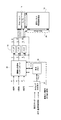
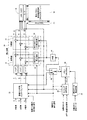
【解決手段】補正演算部29は、入力されてくる画像データとメモリ40からの補正データとで演算を行い、輝度ムラの補正を行う。また、画像入力信号インターフェース32は、メモリ40に画像データを記憶し、この記憶している画像データを出力する。このように、メモリ40には、補正データまたは画像データを選択的に記憶可能である。このように用途に応じてメモリ40に何を記憶するかを切り替えることができる。
【選択図】図8
Description
Claims (2)
- 入力されてくる画像データと各画素の輝度のばらつきを補正するための補正データとで演算を行い、輝度ムラの補正を行うムラ補正手段と、
同じ画像を表示する場合に、記憶している画像データを出力する表示メモリ手段と、
前記ムラ補正手段において用いる補正データ、または前記表示メモリ手段において用いる画像データを選択的に記憶可能なメモリと、
を備え、
前記ムラ補正手段または表示メモリ手段のいずれが前記メモリを使用するかを選択することができるディスプレイ用のドライバIC。 - 請求項1に記載のドライバICを用いた有機ELパネル。
Priority Applications (2)
| Application Number | Priority Date | Filing Date | Title |
|---|---|---|---|
| JP2008068632A JP2009223070A (ja) | 2008-03-18 | 2008-03-18 | ドライバicおよび有機elパネル |
| US12/401,126 US8149190B2 (en) | 2008-03-18 | 2009-03-10 | Correcting brightness variations in organic electroluminescent panel |
Applications Claiming Priority (1)
| Application Number | Priority Date | Filing Date | Title |
|---|---|---|---|
| JP2008068632A JP2009223070A (ja) | 2008-03-18 | 2008-03-18 | ドライバicおよび有機elパネル |
Publications (2)
| Publication Number | Publication Date |
|---|---|
| JP2009223070A true JP2009223070A (ja) | 2009-10-01 |
| JP2009223070A5 JP2009223070A5 (ja) | 2012-11-15 |
Family
ID=41088376
Family Applications (1)
| Application Number | Title | Priority Date | Filing Date |
|---|---|---|---|
| JP2008068632A Pending JP2009223070A (ja) | 2008-03-18 | 2008-03-18 | ドライバicおよび有機elパネル |
Country Status (2)
| Country | Link |
|---|---|
| US (1) | US8149190B2 (ja) |
| JP (1) | JP2009223070A (ja) |
Cited By (3)
| Publication number | Priority date | Publication date | Assignee | Title |
|---|---|---|---|---|
| JP2016515752A (ja) * | 2013-03-27 | 2016-05-30 | コーニンクレッカ フィリップス エヌ ヴェKoninklijke Philips N.V. | 改良型有機発光ダイオード(oled)の光源 |
| KR20170077820A (ko) | 2015-12-28 | 2017-07-06 | 가부시키가이샤 한도오따이 에네루기 켄큐쇼 | 반도체 장치, 드라이버 ic, 및 전자 기기 |
| US10354574B2 (en) | 2015-09-25 | 2019-07-16 | Semiconductor Energy Laboratory Co., Ltd. | Driver IC and electronic device |
Families Citing this family (5)
| Publication number | Priority date | Publication date | Assignee | Title |
|---|---|---|---|---|
| US20150043658A1 (en) * | 2013-08-06 | 2015-02-12 | Raytheon Company | Lower memory bandwidth video non uniformity correction technique |
| CN107293264B (zh) | 2016-04-04 | 2021-07-20 | 株式会社半导体能源研究所 | 显示装置、显示模块以及电子设备 |
| US10290253B2 (en) | 2016-06-10 | 2019-05-14 | Semiconductor Energy Laboratory Co., Ltd. | Semiconductor device, system, and method for operating system |
| US10706779B2 (en) | 2017-02-23 | 2020-07-07 | Synaptics Incorporated | Device and method for image data processing |
| KR20190125311A (ko) | 2017-03-07 | 2019-11-06 | 가부시키가이샤 한도오따이 에네루기 켄큐쇼 | Ic, 드라이버 ic, 표시 시스템, 및 전자 기기 |
Citations (4)
| Publication number | Priority date | Publication date | Assignee | Title |
|---|---|---|---|---|
| JPH10254410A (ja) * | 1997-03-12 | 1998-09-25 | Pioneer Electron Corp | 有機エレクトロルミネッセンス表示装置及びその駆動方法 |
| JP2002251168A (ja) * | 2001-02-22 | 2002-09-06 | Sharp Corp | 表示装置用駆動装置および表示装置 |
| JP2005284172A (ja) * | 2004-03-30 | 2005-10-13 | Eastman Kodak Co | 有機el表示装置 |
| JP2007279290A (ja) * | 2006-04-05 | 2007-10-25 | Eastman Kodak Co | 表示装置 |
Family Cites Families (4)
| Publication number | Priority date | Publication date | Assignee | Title |
|---|---|---|---|---|
| US3828320A (en) * | 1972-12-29 | 1974-08-06 | Burroughs Corp | Shared memory addressor |
| JPH11282420A (ja) | 1998-03-31 | 1999-10-15 | Sanyo Electric Co Ltd | エレクトロルミネッセンス表示装置 |
| US6987496B2 (en) * | 2000-08-18 | 2006-01-17 | Semiconductor Energy Laboratory Co., Ltd. | Electronic device and method of driving the same |
| JP4865986B2 (ja) * | 2003-01-10 | 2012-02-01 | グローバル・オーエルイーディー・テクノロジー・リミテッド・ライアビリティ・カンパニー | 有機el表示装置 |
-
2008
- 2008-03-18 JP JP2008068632A patent/JP2009223070A/ja active Pending
-
2009
- 2009-03-10 US US12/401,126 patent/US8149190B2/en active Active
Patent Citations (4)
| Publication number | Priority date | Publication date | Assignee | Title |
|---|---|---|---|---|
| JPH10254410A (ja) * | 1997-03-12 | 1998-09-25 | Pioneer Electron Corp | 有機エレクトロルミネッセンス表示装置及びその駆動方法 |
| JP2002251168A (ja) * | 2001-02-22 | 2002-09-06 | Sharp Corp | 表示装置用駆動装置および表示装置 |
| JP2005284172A (ja) * | 2004-03-30 | 2005-10-13 | Eastman Kodak Co | 有機el表示装置 |
| JP2007279290A (ja) * | 2006-04-05 | 2007-10-25 | Eastman Kodak Co | 表示装置 |
Cited By (5)
| Publication number | Priority date | Publication date | Assignee | Title |
|---|---|---|---|---|
| JP2016515752A (ja) * | 2013-03-27 | 2016-05-30 | コーニンクレッカ フィリップス エヌ ヴェKoninklijke Philips N.V. | 改良型有機発光ダイオード(oled)の光源 |
| US10354574B2 (en) | 2015-09-25 | 2019-07-16 | Semiconductor Energy Laboratory Co., Ltd. | Driver IC and electronic device |
| KR20170077820A (ko) | 2015-12-28 | 2017-07-06 | 가부시키가이샤 한도오따이 에네루기 켄큐쇼 | 반도체 장치, 드라이버 ic, 및 전자 기기 |
| US9984624B2 (en) | 2015-12-28 | 2018-05-29 | Semiconductor Energy Laboratory Co., Ltd. | Semiconductor device, driver IC, and electronic device |
| US10714004B2 (en) | 2015-12-28 | 2020-07-14 | Semiconductor Energy Laboratory Co., Ltd. | Semiconductor device, driver IC, and electronic device |
Also Published As
| Publication number | Publication date |
|---|---|
| US8149190B2 (en) | 2012-04-03 |
| US20090237334A1 (en) | 2009-09-24 |
Similar Documents
| Publication | Publication Date | Title |
|---|---|---|
| JP5138428B2 (ja) | 表示装置 | |
| JP4055679B2 (ja) | 電気光学装置、電気光学装置の駆動方法及び電子機器 | |
| US8970642B2 (en) | Display device and driving method thereof | |
| JP2009223070A (ja) | ドライバicおよび有機elパネル | |
| US9711080B2 (en) | Timing controller, driving method thereof, and display device using the same | |
| JP4536582B2 (ja) | 表示制御装置及びルックアップテーブルの生成方法 | |
| JP4414354B2 (ja) | 発光表示装置及びその駆動方法 | |
| US9153160B2 (en) | Organic light emitting diode display device with data modulator and a method for driving the same | |
| US9437138B2 (en) | Display device | |
| JP2007279290A (ja) | 表示装置 | |
| US9886887B2 (en) | Device and method for color reduction with dithering | |
| JP2005331891A (ja) | 表示装置 | |
| US20060145979A1 (en) | Liquid crystal display and driving method thereof | |
| KR20110005639A (ko) | 자발광 표시 장치 및 자발광 표시 장치의 구동 방법 | |
| CN105845077A (zh) | 数据补偿器以及包括数据补偿器的显示装置 | |
| CN112242117A (zh) | 显示设备和使用该显示设备驱动显示面板的方法 | |
| JP2003005696A (ja) | 表示データ処理回路及び液晶表示装置 | |
| KR101991337B1 (ko) | 유기발광다이오드 표시장치와 그 구동방법 | |
| KR102463965B1 (ko) | 유기 발광 표시 장치 및 이의 구동 방법 | |
| US20080252567A1 (en) | Active Matrix Display Device | |
| CN112349246A (zh) | 显示装置和驱动显示装置的显示面板的方法 | |
| KR101906310B1 (ko) | 액정표시장치용 타이밍 콘트롤러 및 이의 구동방법 | |
| US9483972B2 (en) | Display device, display method, and electronic system | |
| US20090244102A1 (en) | Lcd, liquid crystal display device, and their drive method | |
| JP2009075240A (ja) | 有機el表示装置 |
Legal Events
| Date | Code | Title | Description |
|---|---|---|---|
| RD03 | Notification of appointment of power of attorney |
Free format text: JAPANESE INTERMEDIATE CODE: A7423 Effective date: 20100319 |
|
| RD04 | Notification of resignation of power of attorney |
Free format text: JAPANESE INTERMEDIATE CODE: A7424 Effective date: 20100423 |
|
| A711 | Notification of change in applicant |
Free format text: JAPANESE INTERMEDIATE CODE: A711 Effective date: 20100520 |
|
| A621 | Written request for application examination |
Free format text: JAPANESE INTERMEDIATE CODE: A621 Effective date: 20110315 |
|
| A521 | Request for written amendment filed |
Free format text: JAPANESE INTERMEDIATE CODE: A523 Effective date: 20120927 |
|
| A871 | Explanation of circumstances concerning accelerated examination |
Free format text: JAPANESE INTERMEDIATE CODE: A871 Effective date: 20120927 |
|
| A977 | Report on retrieval |
Free format text: JAPANESE INTERMEDIATE CODE: A971007 Effective date: 20121112 |
|
| A975 | Report on accelerated examination |
Free format text: JAPANESE INTERMEDIATE CODE: A971005 Effective date: 20121114 |
|
| A131 | Notification of reasons for refusal |
Free format text: JAPANESE INTERMEDIATE CODE: A131 Effective date: 20121120 |
|
| A02 | Decision of refusal |
Free format text: JAPANESE INTERMEDIATE CODE: A02 Effective date: 20130507 |