JP2009187982A - Edge cutting device for solar cell panel - Google Patents
Edge cutting device for solar cell panel Download PDFInfo
- Publication number
- JP2009187982A JP2009187982A JP2008023184A JP2008023184A JP2009187982A JP 2009187982 A JP2009187982 A JP 2009187982A JP 2008023184 A JP2008023184 A JP 2008023184A JP 2008023184 A JP2008023184 A JP 2008023184A JP 2009187982 A JP2009187982 A JP 2009187982A
- Authority
- JP
- Japan
- Prior art keywords
- electrode film
- film
- separation grooves
- insulating
- separation groove
- Prior art date
- Legal status (The legal status is an assumption and is not a legal conclusion. Google has not performed a legal analysis and makes no representation as to the accuracy of the status listed.)
- Granted
Links
Images


Classifications
-
- Y—GENERAL TAGGING OF NEW TECHNOLOGICAL DEVELOPMENTS; GENERAL TAGGING OF CROSS-SECTIONAL TECHNOLOGIES SPANNING OVER SEVERAL SECTIONS OF THE IPC; TECHNICAL SUBJECTS COVERED BY FORMER USPC CROSS-REFERENCE ART COLLECTIONS [XRACs] AND DIGESTS
- Y02—TECHNOLOGIES OR APPLICATIONS FOR MITIGATION OR ADAPTATION AGAINST CLIMATE CHANGE
- Y02E—REDUCTION OF GREENHOUSE GAS [GHG] EMISSIONS, RELATED TO ENERGY GENERATION, TRANSMISSION OR DISTRIBUTION
- Y02E10/00—Energy generation through renewable energy sources
- Y02E10/50—Photovoltaic [PV] energy
Abstract
Description
この発明は、太陽電池パネルの辺縁を処理する縁切り装置に関する。 The present invention relates to an edge cutting device for processing the edge of a solar cell panel.
太陽電池パネルは、ガラスなどの絶縁基板上に電極膜を形成して、この電極膜に光電変換領域毎に電気的に絶縁するための並列する分離溝を加工する。
次に電極膜上にモリブデンなどの光吸収膜が製膜される。
この光吸収膜にも並列する絶縁分離溝を加工する。
さらに、光吸収膜上に硫化亜鉛や硫化インジウムなどの透明電極膜が製膜され、製膜した透明電極膜にも並列する絶縁分離溝を設ける(例えば、特許文献1,2,3,4参照)。
In the solar cell panel, an electrode film is formed on an insulating substrate such as glass, and parallel separation grooves for electrically insulating each photoelectric conversion region are processed in the electrode film.
Next, a light absorption film such as molybdenum is formed on the electrode film.
An insulating separation groove is also formed in parallel with the light absorption film.
Further, a transparent electrode film such as zinc sulfide or indium sulfide is formed on the light absorption film, and an insulating separation groove is provided in parallel with the formed transparent electrode film (see, for example,
なお、周知のように上記各加工ずみ絶縁基板の両側縁に光吸収膜及び透明電極膜をハツリ加工により剥離して電極膜を露出させる。
ところで、各特許文献1,2,3,4に示す太陽電池パネルによると、レーザーの照射により各絶縁分離溝を加工した際、絶縁分離溝端において熱的ダメージにより加工のデブリや各膜の隣接縁及びスクライブラインの端縁の熱溶着にともない導通するので、抵抗値に変化があって不良品の発生原因になる問題があった。
By the way, according to the solar cell panels shown in
また、ニードルによる絶縁分離溝のスクライブの際、絶縁分離溝のスクライブ端において、ニードルが溝端迄達していない場合や、スクライブ残滓が存在している場合などの影響により短絡して問題が発生する。 Further, when the insulating separation groove is scribed by the needle, a problem occurs due to a short circuit due to an influence such as when the needle does not reach the groove end at the scribe end of the insulating separation groove or when a scribe residue is present.
そこで、この発明は、太陽電池パネルの分離溝端側辺縁の電極膜、光吸収層及び透明電極層の縁切りをして上述の問題を解決することにある。 Therefore, the present invention is to solve the above-mentioned problems by cutting off the electrode film, the light absorption layer, and the transparent electrode layer on the side edge of the separation groove end of the solar cell panel.
上記の課題を解決するために、この発明は、ガラスなどの絶縁基板上に製膜してある電極膜に光電変換領域毎に電気的に絶縁するための並列する分離溝を加工したのち、上記電極膜上に製膜してある光吸収膜に上記分離溝に平行する多数条の絶縁分離溝を加工し、次いで光吸収膜上製膜してある透明電極膜に上記分離溝に平行する絶縁分離溝を加工したのち、上記電極膜の上記分離溝に平行する両側縁が露出するように上層の上記光吸収膜及び透明電極膜を剥離除去した太陽電池パネル素板において、この素板を荷受けするテーブルと、このテーブル上の上記素板の分離溝端側辺縁の上下いずれか片方に配置して上記電極膜にレーザーを照射して絶縁分離溝を形成するレーザーヘッド及び上記光吸収膜・透明電極膜の上記レーザーヘッドによる形成絶縁分離溝に沿う線上に絶縁分離溝をスクライブにより形成するように昇降手段を介し設けたニードルとからなり、上記テーブル或いは上下のレーザーヘッド、ニードルのいずれか片方を走行手段により分離溝形成方向に走行させるようにした構成を採用する。 In order to solve the above-described problems, the present invention processes the separation grooves arranged in parallel for electrically insulating each photoelectric conversion region in an electrode film formed on an insulating substrate such as glass, and then A plurality of insulating separation grooves parallel to the separation grooves are processed on the light absorption film formed on the electrode film, and then the insulation separation parallel to the separation grooves is formed on the transparent electrode film formed on the light absorption film. After processing the groove, in the solar cell panel base plate from which the light absorption film and the transparent electrode film of the upper layer are peeled and removed so that both side edges parallel to the separation groove of the electrode film are exposed, the base plate is received. A laser head that is arranged on either the upper or lower side of the separation groove end side edge of the base plate on the table and irradiates the electrode film with a laser to form an insulating separation groove, and the light absorbing film / transparent electrode With the above laser head of the film It comprises a needle provided through an elevating means so as to form an insulating separation groove by scribing on a line along the formed insulating separation groove, and either one of the table or the upper and lower laser heads or the needle is driven by the traveling means in the direction of forming the separation groove A configuration that allows the vehicle to run is adopted.
すると、太陽電池パネルの電極膜の分離溝両端側を照射するレーザーにより剥離除去され、又光吸収層及び透明電極層の分離溝の両端側をニードルによりスクライブして、導通(短絡)による不都合をなくすることができる。 Then, the both sides of the separation groove of the electrode film of the solar cell panel are peeled and removed by the laser, and both ends of the separation groove of the light absorption layer and the transparent electrode layer are scribed with a needle, thereby causing inconvenience due to conduction (short circuit). Can be eliminated.
以上のように、この発明の太陽電池パネルの縁切り装置によれば、テーブル上に太陽電池パネル素板を荷受けして、テーブル或いは対向するレーザーヘッド、昇降手段により降下させたニードルの片方を走行手段によって走行させることで、太陽電池パネル素板の絶縁基板上の製膜電極膜をレーザーヘッドから照射するレーザーにより電極膜を分離しながら絶縁分離溝を加工し、又電極膜上の積層透明膜及び光吸収膜に電極膜の加工絶縁分離溝の線上にニードルでスクライブしながら絶縁分離溝を加工することができる。 As described above, according to the edge cutting device of the solar cell panel of the present invention, the solar cell panel base plate is received on the table, and one of the needles lowered by the table or the opposed laser head and the lifting / lowering means is traveled. The insulating separation groove is processed while separating the electrode film with a laser that irradiates the film-forming electrode film on the insulating substrate of the solar cell panel base plate from the laser head, and the laminated transparent film on the electrode film and The insulating separation groove can be processed while scribing with a needle on the line of the processed insulating separation groove of the electrode film in the light absorption film.
このため、電極膜、光吸収膜及び透明電極膜の膜毎に加工してある絶縁分離溝端の熱的ダメージや熱溶着などにより導通して、抵抗値に変化があるなどの不都合を太陽電池パネル素板の縁切りによりなくすることができる。 For this reason, the solar cell panel has a disadvantage in that the resistance value changes due to conduction due to thermal damage or thermal welding at the end of the insulating separation groove processed for each electrode film, light absorption film and transparent electrode film. This can be eliminated by cutting the base plate.
この発明の実施の形態を添付図面に基づいて説明する。
この発明の実施形態の縁切り加工を施す太陽電池パネルの素板Aは、図4に示すように、まず、ガラスなどの絶縁基板1上に製膜した電極膜2には、一方の対向する二辺縁に沿って多数条の並列する絶縁分離溝3が(この絶縁分離溝3は、レーザーヘッドから分離溝幅に通した出力の照射レーザーを結像させて電極膜2を分離させながら加工する)設けてあり、次いで絶縁分離溝3の加工ずみ電極膜2上にモリブデンなどの光吸収膜4を製膜したのち、この製膜光吸収膜4には、各絶縁分離溝3の線上にニードルによりスクライブしながら並列絶縁分離溝5が加工され、その後に絶縁分離溝5の加工ずみ光吸収膜4上に硫化亜鉛や硫化インジウムなどの透明電極膜6を製膜したのち、この製膜透明電極膜6には、各絶縁分離溝5の線上にニードルによりスクライブしながら並列絶縁分離溝7が加工され、然るのち、両サイドの絶縁分離溝7の外側の透明電極膜6及び光吸収膜4の絶縁基板1の側面から内方所定の幅を刃物によりハツリ加工して電極膜2を露出させたものである。
Embodiments of the present invention will be described with reference to the accompanying drawings.
As shown in FIG. 4, the base plate A of the solar cell panel to be subjected to edge cutting according to the embodiment of the present invention has two
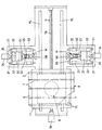
次に、上記素板Aの縁切り加工を図1から図3に基づいて説明する。
まずテーブル11上に上記の素板Aを載置して荷受けする。
荷受けした素板Aをテーブル11上で保持する。
Next, the edge cutting process of the base plate A will be described with reference to FIGS.
First, the base plate A is placed on the table 11 and received.
The received base plate A is held on the table 11.
上記の保持方法としては、中空のテーブル11の頂壁に無数の小孔12群を設けて、テーブル11内を吸引して保持するようになっている。
As the above holding method, an infinite number of
このとき、素板Aの縁切り両端部がテーブル11の辺縁から外方に食み出すように突出させて荷受けする。 At this time, both edge portions of the base plate A are projected so as to protrude outward from the edge of the table 11 and are received.
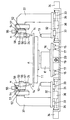
また、テーブル11から食み出した辺の下側に電極膜2に絶縁分離溝Xの加工に適した出力のレーザーを上方に照射するレーザーヘッド13が、このレーザーヘッド13に対向させて絶縁分離溝Xに合致した直上に光吸収膜4にスクライブにより絶縁分離溝Y及び透明電極膜6にスクライブにより絶縁分離溝Zを加工するための昇降手段Hにより昇降するニードル14が設けてあり、テーブル11或いはレーザーヘッド13とニードル14とのいずれか片方を走行手段Sにより進退走行させるようになっている。
Further, a
上記の走行手段Sは、図示の場合、二条の平行するレール15にテーブル11の搭載走行台車16の下面両側のスライダ17をスライド自在に係合すると共に、モーター18の運転により可逆回転する雄ネジ19の両端を軸承して、この雄ネジ19に走行台車16に支持させた雌ネジ20をねじ込んでテーブル11を進退走行するようにしたが、限定されず、テーブル11の定置式に対しレーザーヘッド13とニードル14側を進退走行させるようにしてもよい。
In the illustrated case, the traveling means S includes a male screw that reversibly rotates by operating the
そして、図示の場合レーザーヘッド13とニードル14とをテーブル11の走行路の両側に配置して、素板Aの両端縁を同時に縁切り加工するようにしたが、限定されず、レーザーヘッド13とニードル14とをテーブル11の走行路の片側のみに設け、走行台車16に旋回手段Eを介しテーブル11を搭載し、テーブル11の180度回転により素板Aの片端側、次いでもう片端側を縁切り加工するようにしてもよい。
In the illustrated case, the
また、図1、3に示すように、テーブル11の走行路の両側にレール31に台車32の下面両側のスライダ33をスライド自在に係合すると共に、モーター34の運転により可逆駆動する雄ネジ35に台車32に支持させた雌ネジ36をねじ込み、台車32上にレーザーヘッド13を据え付け、台車32上の柱37にニードル14を有する昇降手段Hを据え付けることで、左右のレーザーヘッド13とニードル14との位置を調整することができる。
Further, as shown in FIGS. 1 and 3, a
上記の昇降手段Hは、図示の場合、台車32上の柱37に設けた縦方向のレール51と、このレール51にスライド自在に係合したスライダ52を有する昇降体53と、この昇降体53の上端からねじ込んだボールネジ54と、柱37側に支持させてボールネジ54を可逆駆動するモーター55とで構成され、昇降体53には、支持部材56を介し下端のホルダ24にニードル14を有する軸材57が支持させてある。
In the illustrated case, the lifting means H includes a
上記のように構成すると、数値制御によりモーター55を運転してボールネジ54をドライブすることにより昇降体53と共に軸材57、ホルダ24及びニードル14が降下して、ニードル14によるスクライブ深さが決定するようにしてあるが、上述の構成に限定されず、上記の目的を達成する昇降手段Hを採用してもよい。
If comprised as mentioned above, the
そして、軸材57の上端にシリンダ58による押圧力を付与しておくと、スクライブの際のニードル14の上下の微動を許容して、スクライブの追従をスムーズにすることができる。
And if the pressing force by the
上記のように構成すると、素板Aの端部にニードル14により透明電極膜6及び光吸収膜4をスクライブして絶縁分離溝Z、Yが加工され、レーザーヘッド13からのレーザーの照射により絶縁分離溝Xが加工される。
When configured as described above, the
その結果、電極膜2、光吸収膜4及び透明電極膜6に膜毎加工してある絶縁分離溝3、5、7端の熱的ダメージや熱溶着などにより導通して抵抗値に変化があるなどの不都合を縁切りによりなくすることができる。
なお、上述の実施例において、素板Aの下方にレーザーヘッド13を、素板Aの上方にニードル14を対向させて配置したが、限定されず、図6に示すように素板Aの上側にニードル14とレーザーヘッド13とを並列状(走行手段Sの走行方向に並べて)に配置することもできる。
As a result, resistance is changed due to conduction due to thermal damage or thermal welding at the ends of the
In the above-described embodiment, the
A 素板
1 絶縁基板
2 電極膜
3 分離溝
4 光吸収膜
5 分離溝
6 透明電極膜
7 分離溝
11 テーブル
12 小孔
13 レーザーヘッド
14 ニードル
S 走行手段
15 レール
16 走行台車
17 スライダ
18 モーター
19 雄ネジ
20 雌ネジ
E 旋回手段
H 昇降手段
24 ホルダ
31 レール
32 台車
33 スライダ
34 モーター
35 雄ネジ
36 雌ネジ
37 柱
51 レール
52 スライダ
53 昇降体
54 ボールネジ
55 モーター
56 支持部材
57 軸材
58 シリンダ
X、Y、Z 分離溝
A Substrate 1
Claims (1)
Priority Applications (1)
| Application Number | Priority Date | Filing Date | Title |
|---|---|---|---|
| JP2008023184A JP5137187B2 (en) | 2008-02-01 | 2008-02-01 | Solar panel trimming device |
Applications Claiming Priority (1)
| Application Number | Priority Date | Filing Date | Title |
|---|---|---|---|
| JP2008023184A JP5137187B2 (en) | 2008-02-01 | 2008-02-01 | Solar panel trimming device |
Publications (2)
| Publication Number | Publication Date |
|---|---|
| JP2009187982A true JP2009187982A (en) | 2009-08-20 |
| JP5137187B2 JP5137187B2 (en) | 2013-02-06 |
Family
ID=41070976
Family Applications (1)
| Application Number | Title | Priority Date | Filing Date |
|---|---|---|---|
| JP2008023184A Expired - Fee Related JP5137187B2 (en) | 2008-02-01 | 2008-02-01 | Solar panel trimming device |
Country Status (1)
| Country | Link |
|---|---|
| JP (1) | JP5137187B2 (en) |
Cited By (4)
| Publication number | Priority date | Publication date | Assignee | Title |
|---|---|---|---|---|
| JP2011147953A (en) * | 2010-01-20 | 2011-08-04 | Disco Abrasive Syst Ltd | Laser machining device |
| KR101149766B1 (en) * | 2010-12-21 | 2012-06-11 | (주)미래컴퍼니 | Device and method for machining multi-layer substrate performing isolation process and edge deletion process |
| KR101226201B1 (en) | 2010-11-18 | 2013-01-28 | 미쓰보시 다이야몬도 고교 가부시키가이샤 | Defect repairing tool, defect repairing device and defect repairing method for thin-film solar cell |
| CN115351010A (en) * | 2022-08-31 | 2022-11-18 | 华工法利莱切焊系统工程有限公司 | Laser clearing system and method for lithium battery cell insulation protective film |
Citations (6)
| Publication number | Priority date | Publication date | Assignee | Title |
|---|---|---|---|---|
| JPS63283077A (en) * | 1987-05-14 | 1988-11-18 | Fuji Electric Co Ltd | Manufacture of solar cell |
| JPH10125632A (en) * | 1996-10-23 | 1998-05-15 | Mitsubishi Heavy Ind Ltd | Method and apparatus for laser etching |
| JP2001339081A (en) * | 2000-03-23 | 2001-12-07 | Matsushita Electric Ind Co Ltd | Solar cell and method of manufacturing the same |
| JP2002016269A (en) * | 2000-06-28 | 2002-01-18 | Mitsubishi Heavy Ind Ltd | Method and apparatus for manufacturing thin-film solar cell panel |
| JP2004115356A (en) * | 2002-09-26 | 2004-04-15 | Honda Motor Co Ltd | Mechanical scribing apparatus |
| JP2007273622A (en) * | 2006-03-30 | 2007-10-18 | Kaneka Corp | Photoelectric conversion device and manufacturing method thereof |
-
2008
- 2008-02-01 JP JP2008023184A patent/JP5137187B2/en not_active Expired - Fee Related
Patent Citations (6)
| Publication number | Priority date | Publication date | Assignee | Title |
|---|---|---|---|---|
| JPS63283077A (en) * | 1987-05-14 | 1988-11-18 | Fuji Electric Co Ltd | Manufacture of solar cell |
| JPH10125632A (en) * | 1996-10-23 | 1998-05-15 | Mitsubishi Heavy Ind Ltd | Method and apparatus for laser etching |
| JP2001339081A (en) * | 2000-03-23 | 2001-12-07 | Matsushita Electric Ind Co Ltd | Solar cell and method of manufacturing the same |
| JP2002016269A (en) * | 2000-06-28 | 2002-01-18 | Mitsubishi Heavy Ind Ltd | Method and apparatus for manufacturing thin-film solar cell panel |
| JP2004115356A (en) * | 2002-09-26 | 2004-04-15 | Honda Motor Co Ltd | Mechanical scribing apparatus |
| JP2007273622A (en) * | 2006-03-30 | 2007-10-18 | Kaneka Corp | Photoelectric conversion device and manufacturing method thereof |
Cited By (6)
| Publication number | Priority date | Publication date | Assignee | Title |
|---|---|---|---|---|
| JP2011147953A (en) * | 2010-01-20 | 2011-08-04 | Disco Abrasive Syst Ltd | Laser machining device |
| CN102151996A (en) * | 2010-01-20 | 2011-08-17 | 株式会社迪思科 | Laser processing device |
| KR101226201B1 (en) | 2010-11-18 | 2013-01-28 | 미쓰보시 다이야몬도 고교 가부시키가이샤 | Defect repairing tool, defect repairing device and defect repairing method for thin-film solar cell |
| KR101149766B1 (en) * | 2010-12-21 | 2012-06-11 | (주)미래컴퍼니 | Device and method for machining multi-layer substrate performing isolation process and edge deletion process |
| CN115351010A (en) * | 2022-08-31 | 2022-11-18 | 华工法利莱切焊系统工程有限公司 | Laser clearing system and method for lithium battery cell insulation protective film |
| CN115351010B (en) * | 2022-08-31 | 2024-02-20 | 华工法利莱切焊系统工程有限公司 | Laser cleaning system and method for insulating protective film of lithium battery cell |
Also Published As
| Publication number | Publication date |
|---|---|
| JP5137187B2 (en) | 2013-02-06 |
Similar Documents
| Publication | Publication Date | Title |
|---|---|---|
| CN106346148B (en) | Method for producing polycrystalline SiC wafer | |
| KR101200788B1 (en) | Method and apparatus for processing substrate of brittle material | |
| KR101786436B1 (en) | Scribing apparatus of the substrate | |
| KR101193929B1 (en) | Scribe apparatus for thin film solar cell | |
| JP5137187B2 (en) | Solar panel trimming device | |
| KR102267989B1 (en) | Processing method of package substrate | |
| US20150059411A1 (en) | Method of separating a glass sheet from a carrier | |
| TWI472050B (en) | Production of integrated thin film solar cells | |
| WO2010098307A1 (en) | Method for manufacturing integrated thin film solar cell | |
| KR101579922B1 (en) | Method and device for producing edge cutouts in sheet glass | |
| JP2011156582A (en) | Dividing method by co2 laser | |
| US20080057680A1 (en) | Wafer laser processing method | |
| JP2007157659A (en) | Forming method of wiring pattern of organic el element and forming device of organic el element | |
| JP6202308B2 (en) | Method for producing compound thin film solar cell | |
| JP5357580B2 (en) | Grooving tool and method of grooving thin film solar cell using the same | |
| WO2010103947A1 (en) | Grooving tool for thin film solar cell | |
| KR101512705B1 (en) | Groove processing tool, and groove processing method and groove processing apparatus for thin film solar cell using the same | |
| JP2011216646A (en) | Scribing device | |
| JP2009187981A (en) | Scribing tool for solar cell panel | |
| WO2011027533A1 (en) | Method and apparatus for manufacturing a thin-film solar battery | |
| JP2009142872A (en) | Laser etching apparatus | |
| CN215731746U (en) | Solar energy component scribing device | |
| JP2020107800A (en) | Groove processing tool, and grooving method and grooving apparatus for thin film solar cell using the same | |
| JP2011162395A (en) | Substrate working apparatus | |
| JP2020107796A (en) | Groove processing tool, and grooving method and grooving apparatus for thin film solar cell using the same |
Legal Events
| Date | Code | Title | Description |
|---|---|---|---|
| A621 | Written request for application examination |
Free format text: JAPANESE INTERMEDIATE CODE: A621 Effective date: 20110131 |
|
| A977 | Report on retrieval |
Free format text: JAPANESE INTERMEDIATE CODE: A971007 Effective date: 20111207 |
|
| A131 | Notification of reasons for refusal |
Free format text: JAPANESE INTERMEDIATE CODE: A131 Effective date: 20120110 |
|
| TRDD | Decision of grant or rejection written | ||
| A01 | Written decision to grant a patent or to grant a registration (utility model) |
Free format text: JAPANESE INTERMEDIATE CODE: A01 Effective date: 20121009 |
|
| A01 | Written decision to grant a patent or to grant a registration (utility model) |
Free format text: JAPANESE INTERMEDIATE CODE: A01 |
|
| A61 | First payment of annual fees (during grant procedure) |
Free format text: JAPANESE INTERMEDIATE CODE: A61 Effective date: 20121109 |
|
| R150 | Certificate of patent or registration of utility model |
Free format text: JAPANESE INTERMEDIATE CODE: R150 |
|
| FPAY | Renewal fee payment (event date is renewal date of database) |
Free format text: PAYMENT UNTIL: 20151122 Year of fee payment: 3 |
|
| R250 | Receipt of annual fees |
Free format text: JAPANESE INTERMEDIATE CODE: R250 |
|
| LAPS | Cancellation because of no payment of annual fees |