JP2009181704A - Backlight device - Google Patents
Backlight device Download PDFInfo
- Publication number
- JP2009181704A JP2009181704A JP2008017348A JP2008017348A JP2009181704A JP 2009181704 A JP2009181704 A JP 2009181704A JP 2008017348 A JP2008017348 A JP 2008017348A JP 2008017348 A JP2008017348 A JP 2008017348A JP 2009181704 A JP2009181704 A JP 2009181704A
- Authority
- JP
- Japan
- Prior art keywords
- submount
- led
- substrate
- backlight device
- led chips
- Prior art date
- Legal status (The legal status is an assumption and is not a legal conclusion. Google has not performed a legal analysis and makes no representation as to the accuracy of the status listed.)
- Withdrawn
Links
Images


Classifications
-
- H—ELECTRICITY
- H01—ELECTRIC ELEMENTS
- H01L—SEMICONDUCTOR DEVICES NOT COVERED BY CLASS H10
- H01L2224/00—Indexing scheme for arrangements for connecting or disconnecting semiconductor or solid-state bodies and methods related thereto as covered by H01L24/00
- H01L2224/01—Means for bonding being attached to, or being formed on, the surface to be connected, e.g. chip-to-package, die-attach, "first-level" interconnects; Manufacturing methods related thereto
- H01L2224/42—Wire connectors; Manufacturing methods related thereto
- H01L2224/47—Structure, shape, material or disposition of the wire connectors after the connecting process
- H01L2224/48—Structure, shape, material or disposition of the wire connectors after the connecting process of an individual wire connector
- H01L2224/4805—Shape
- H01L2224/4809—Loop shape
- H01L2224/48091—Arched
Abstract
Description
本発明は、テレビジョン装置等の表示装置の光源に用いられるバックライト装置に関する。 The present invention relates to a backlight device used as a light source of a display device such as a television device.
従来から、照明対象に白色光を照射するための複数種の発光ダイオード(LED)素子を有するLEDランプを素子搭載基板上に複数個搭載してなるバックライト装置が知られている(例えば、特許文献1参照)。特許文献1に記載のバックライト装置は、素子搭載基板が同一平面内で隣接する位置に複数個配置され、複数個の素子搭載基板のうち互いに隣接する2つの素子搭載基板は着脱可能に連結されている。そして、赤色LED素子、緑色LED素子及び青色LED素子が、半球状の光学形状面を有する透明性樹脂からなる封止部材によってそれぞれ封止されている。このバックライト装置によれば、LEDランプの修理、点検等を素子搭載基板ごとに行うことができ、製造・交換等コストの低廉化を図ることができる。
ところで、特許文献1に記載のバックライト装置では、各LED素子を基板上にて別個に封止しているため、各LED素子間の距離が大きくなる。従って、各LED素子から発せられた光を混合させるために、照明対象をバックライト装置から十分に距離をおいて配置する必要がある。従って、テレビジョン装置等の表示装置の薄型化に限界があった。また、製造、交換等コストのさらなる低廉化が望まれている。
By the way, in the backlight apparatus of
本発明は、前記事情に鑑みてなされたものであり、その目的とするところは、各LED素子から発せられる光を基板の近くで混合させることができ、製造、交換等コストのさらなる低廉化を図ることのできるバックライト装置を提供することにある。 The present invention has been made in view of the above circumstances, and the object thereof is to allow light emitted from each LED element to be mixed in the vicinity of the substrate, and to further reduce costs such as manufacturing and replacement. An object of the present invention is to provide a backlight device that can be realized.
前記目的を達成するため、本発明では、複数のLED素子と、前記複数のLED素子が搭載されるサブマウントと、前記サブマウントが搭載され、電極パターンが形成される基板と、前記複数のLED素子ごとに設けられ、前記LED素子の電極と前記基板の前記電極パターンとを直接的に接続するワイヤと、を備えたバックライト装置が提供される。 In order to achieve the above object, in the present invention, a plurality of LED elements, a submount on which the plurality of LED elements are mounted, a substrate on which the submount is mounted and an electrode pattern is formed, and the plurality of LEDs There is provided a backlight device that is provided for each element and includes a wire that directly connects the electrode of the LED element and the electrode pattern of the substrate.
上記バックライト装置において、前記サブマウントには、赤色光を発するLED素子、緑色光を発するLED素子及び青色光を発するLED素子が搭載されることが好ましい。 In the backlight device, it is preferable that an LED element that emits red light, an LED element that emits green light, and an LED element that emits blue light are mounted on the submount.
上記バックライト装置において、前記複数のLED素子、前記サブマウント及び前記ワイヤを封止する封止材を備えることが好ましい。 The backlight device preferably includes a sealing material that seals the plurality of LED elements, the submount, and the wire.
上記バックライト装置において、前記封止材の表面は、前記複数のLED素子から発せられた光を拡散させる拡散形状をなすことが好ましい。 The said backlight apparatus WHEREIN: It is preferable that the surface of the said sealing material makes the spreading | diffusion shape which diffuses the light emitted from these LED element.
上記バックライト装置において、前記サブマウントはアルミナからなることが好ましい。 In the backlight device, the submount is preferably made of alumina.
本発明によれば、各LED素子から発せられる光を基板の近くで混合させることができ、製造、交換等コストのさらなる低廉化を図ることができる。 According to the present invention, the light emitted from each LED element can be mixed in the vicinity of the substrate, and the cost can be further reduced, such as manufacturing and replacement.
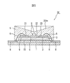
図1から図3は本発明の一実施形態を示すもので、図1はバックライト装置の概略外観斜視図である。 1 to 3 show an embodiment of the present invention, and FIG. 1 is a schematic external perspective view of a backlight device.
図1に示すように、バックライト装置1は、複数のLEDチップ21,22,23と、各LEDチップ21,22,23を搭載するサブマウント3と、サブマウント3を搭載する樹脂製の基板4と、各LEDチップ21,22,23をサブマウント3とともに封止する封止樹脂5と、を備えている。バックライト装置1は表示装置としてのテレビジョン装置の光源として用いられ、複数のサブマウント3が矩形状の基板4上にて規則的に配置されている。
As shown in FIG. 1, the
図2はバックライト装置の概略平面図である。
図2に示すように、各サブマウント3は平面視にて正方形状を呈し、1つのサブマウント3に4つのLEDチップ21,22,23が搭載されている。各サブマウント3は、白色を呈するとともに多孔質状の材料に形成される。本実施形態においては、各サブマウント3は、アルミナにより形成されている。
FIG. 2 is a schematic plan view of the backlight device.
As shown in FIG. 2, each
4つのLEDチップ21,22,23は、各サブマウント3の上面の外縁近傍に設けられる。本実施形態においては、各LEDチップ21,22,23は、サブマウント3の四辺の中央付近にそれぞれ搭載されている。本実施形態においては、サブマウント3には、赤色光を発するLEDチップ21が1つ、緑色光を発するLEDチップ22が2つ、青色光をLEDチップ23が1つ、それぞれ搭載されている。各LEDチップ21,22,23の材質は任意であり、発光波長等の仕様に応じて、InGaN系、GaN系、AlGaN系、ZnSe系、AlGaInP系、GaP系、GaAsP系等の材料を選択することができる。
The four
各LEDチップ21,22,23は、アノード電極及びカソード電極が上面に設けられるフェイスアップ型であり、基板4上に形成された電極パターン8とワイヤ6により電気的に接続される。本実施形態においては、各LEDチップ21,22,23にそれぞれ設けられるアノード側及びカソード側の2つのワイヤ6は、ほぼ平行に形成されている。
Each
基板4は、ガラスエポキシ樹脂を基材とし、最外層に白色のソルダーレジスト層7が配置されたFR−4基板である。基板4の電極パターン8は、表面がAuからなり、ワイヤ6との接触部分がソルダーレジスト層7から露出している。本実施形態においては、電極パターン8は1つのLEDチップ21,22,23について隣接して2つ設けられる。
The substrate 4 is an FR-4 substrate having a glass epoxy resin as a base material and a white solder resist layer 7 disposed on the outermost layer. The surface of the
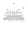
図3はバックライト装置の一部断面図である。
図3に示すように、各LEDチップ21,22,23はダイボンドペースト9を介してサブマウント3に固定され、サブマウント3はダイボンドペースト10を介して基板4に固定されている。ここで、サブマウント3は多孔質材であることから、ダイボンドペースト9,10による接着力を大きくすることができ、各LEDチップ21,22,23とサブマウント3並びにサブマウント3と基板4とを強固に接着することができる。
FIG. 3 is a partial cross-sectional view of the backlight device.
As shown in FIG. 3, each
本実施形態においては、ワイヤ6は、基板4の電極パターン8との接触部をファーストボンドとし、各LEDチップ21,22,23との接触部をセカンドボンドとしている。これにより、各LEDチップ21,22,23との接触部をファーストボンドとする場合よりも、ワイヤ6の基板4からの高さを低くすることができ、ワイヤ6の封止に必要な封止樹脂5の高さが比較的低くなっている。
In this embodiment, the
封止材としての封止樹脂5は、シリコーン、エポキシ樹脂等の透明樹脂からなり、各LEDチップ21,22,23、サブマウント3及びワイヤ6を封止する。本実施形態においては、封止樹脂5は、直方体状を呈し、上面及び側面が平坦に形成されている。尚、封止材は樹脂に限定されず、ガラス等の無機材を用いることも可能である。
The sealing
以上のように構成されたバックライト装置1では、サブマウント3上の各LEDチップ21,22,23が基板4の電極パターン8とワイヤ6により直接的に接続されることから、ワイヤ6の設置に要するスペースを小さくすることができる。例えば、ワイヤ6をサブマウント3を接続した場合は、サブマウント3にワイヤ6を接続するためのスペースが必要となり、サブマウント3上にて各LEDチップ21,22,23を互いに十分に近づけることはできない。
In the
このように、各LEDチップ21,22,23を互いに近接して配置することができるので、各LEDチップ21,22,23から発せられる光を基板4の近傍にて混合させることができる。これに加え、各LEDチップ21,22,23が封止樹脂5により一括して封止されているので、各LEDチップ21,22,23から発せられる光を封止樹脂5内で混合させることができる。従って、各LEDチップ21,22,23の光の混合に必要な基板4からの距離を小さくし、被照射体との距離を小さくすることができる。
Thus, since each
これにより、被照射体が液晶表示部であるテレビジョン装置において、波長の異なる光の混色性を確保し、かつ、バックライト装置1と液晶表示部との距離を小さくし、テレビジョン装置の厚さを飛躍的に薄くすることができる。すなわち、本実施形態のバックライト装置1は、光の混色を重視すると液晶表示部とバックライト装置との距離が大きくなって厚さ寸法が大きくなり、薄型化を図るべく液晶表示部とバックライト装置の距離を小さくすると混色性が悪化するという、液晶のテレビジョン装置に固有の問題を解決したものである。特に、本実施形態においては、封止樹脂5の上面が平坦に形成されているので、各LEDチップ21,22,23から発せられる光が封止樹脂5と空気との界面において反射し易く、封止樹脂5内で各LEDチップ21,22,23の光を効率よく混合させることができる。
Accordingly, in the television device in which the irradiated object is a liquid crystal display unit, the color mixing property of light having different wavelengths is ensured, the distance between the
また、各LEDチップ21,22,23をサブマウント3に搭載した状態で基板4に搭載することができ、各LEDチップ2を基板4に直接搭載する場合よりも、各LEDチップ21,22,23の基板4への搭載が容易である。また、各LEDチップ21,22,23の点検をサブマウント3単位で行うことができ、装置の歩留まりが向上して製造コストの低廉化を図ることができる。また、各LEDチップ21,22,23に不具合等が生じた場合に、サブマウント3単位で部品交換を行えばよく、メンテナンス性が良好である。
Further, each
また、各LEDチップ21,22,23から放射される光はサブマウント3にて反射し、基板4のソルダーレジスト層7へ直接的に入射することはない。また、各LEDチップ21,22,23にて生じる熱はサブマウント3に放散される。これにより、LEDチップ21,22,23から放射される光、熱等による基板4のソルダーレジスト層7の劣化が抑制される。
Further, the light emitted from each
尚、前記実施形態においては、サブマウント3がアルミナからなるものを示したが、例えば、サブマウント3をアルミニウムとしたり、サブマウント3の本体をアルミナとしてサブマウント3の上面にアルミニウム膜を形成してもよく、任意の金属、セラミックを用いることができる。さらには、サブマウント3を樹脂としてもよい。
In the above embodiment, the
また、前記実施形態においては、封止樹脂5が平坦な上面を有する直方体状に形成されたものを示したが、例えば図4、図5及び図6に示すように、封止樹脂5の上面が各LEDチップ21,22,23から発せられた光を拡散させる形状であってもよい。図4のバックライト装置101では、封止樹脂5は、直方体状に形成され、上面105aが粗面化加工されている。図5のバックライト装置201では、封止樹脂5は、円柱形状に形成され、上面205aが外縁から中心へ向かって基板4側へ下がるよう傾斜して形成されている。また、図6のバックライト装置301では、封止樹脂5は、円柱形状に形成され、上面には外縁から中心へ向かって湾曲して下る断面放物線状の区間305aと、基板4に対して垂直な区間305bとが交互に形成されている。尚、封止樹脂5の拡散形状は、これらの形状に限定されるものでなく、例えば断面にて上面が鋸歯状を呈するものであってもよい。
Moreover, in the said embodiment, although the sealing
また、前記実施形態においては、サブマウント3に搭載される全てのLEDチップ21,22,23が、上面にアノード電極及びカソード電極の2つの電極が配置されるものを示したが、上面及び下面に1つずつ電極が配置されるものであってもよい。この場合、サブマウント3には、LEDチップの下面と基板の電極パターンとを電気的に接続する配線部が必要となる。
Moreover, in the said embodiment, although all the LED chips 21, 22, and 23 mounted in the
また、前記実施形態においては、1つのサブマウント3に対し、赤色のLEDチップ21が1つ、緑色のLEDチップ22が2つ、青色のLEDチップ23が1つ搭載されるものを示したが、搭載されるLEDチップの個数や発光波長はこれに限定されるものではない。
In the above embodiment, one
また、前記実施形態においては、基板4として難燃性がFR−4のものを示したが、基板4は例えばFR−5であってもよいし、その他、具体的な細部構造等についても適宜に変更可能であることは勿論である。 Moreover, in the said embodiment, although the thing with a flame retardance of FR-4 was shown as the board | substrate 4, the board | substrate 4 may be FR-5, for example, and also about a specific detailed structure etc. suitably. Of course, it can be changed.
1 バックライト装置
3 サブマウント
4 基板
5 封止樹脂
6 ワイヤ
7 ソルダーレジスト層
8 電極パターン
9 ダイボンドペースト
10 ダイボンドペースト
21 LEDチップ
22 LEDチップ
23 LEDチップ
101 バックライト装置
105a 上面
201 バックライト装置
205a 上面
301 バックライト装置
305a 断面放物線状の区間
305b 垂直な区間
DESCRIPTION OF
Claims (5)
前記複数のLED素子が搭載されるサブマウントと、
前記サブマウントが搭載され、電極パターンが形成される基板と、
前記複数のLED素子ごとに設けられ、前記LED素子の電極と前記基板の前記電極パターンとを直接的に接続するワイヤと、を備えたバックライト装置。 A plurality of LED elements;
A submount on which the plurality of LED elements are mounted;
A substrate on which the submount is mounted and an electrode pattern is formed;
A backlight device comprising: a wire provided for each of the plurality of LED elements and directly connecting an electrode of the LED element and the electrode pattern of the substrate.
Priority Applications (1)
| Application Number | Priority Date | Filing Date | Title |
|---|---|---|---|
| JP2008017348A JP2009181704A (en) | 2008-01-29 | 2008-01-29 | Backlight device |
Applications Claiming Priority (1)
| Application Number | Priority Date | Filing Date | Title |
|---|---|---|---|
| JP2008017348A JP2009181704A (en) | 2008-01-29 | 2008-01-29 | Backlight device |
Publications (2)
| Publication Number | Publication Date |
|---|---|
| JP2009181704A true JP2009181704A (en) | 2009-08-13 |
| JP2009181704A5 JP2009181704A5 (en) | 2010-04-08 |
Family
ID=41035529
Family Applications (1)
| Application Number | Title | Priority Date | Filing Date |
|---|---|---|---|
| JP2008017348A Withdrawn JP2009181704A (en) | 2008-01-29 | 2008-01-29 | Backlight device |
Country Status (1)
| Country | Link |
|---|---|
| JP (1) | JP2009181704A (en) |
Cited By (2)
| Publication number | Priority date | Publication date | Assignee | Title |
|---|---|---|---|---|
| JP2014192407A (en) * | 2013-03-28 | 2014-10-06 | Citizen Electronics Co Ltd | Semiconductor light-emitting device |
| JP2017038031A (en) * | 2015-08-14 | 2017-02-16 | シチズン電子株式会社 | Light emitting device and manufacturing method for the same |
Citations (4)
| Publication number | Priority date | Publication date | Assignee | Title |
|---|---|---|---|---|
| JP2006339542A (en) * | 2005-06-03 | 2006-12-14 | Citizen Electronics Co Ltd | Chip led |
| JP2007116125A (en) * | 2005-09-20 | 2007-05-10 | Matsushita Electric Works Ltd | Light emitting device |
| JP2007157686A (en) * | 2005-11-11 | 2007-06-21 | Hitachi Displays Ltd | Lighting system and liquid crystal display device using it |
| JP2007324204A (en) * | 2006-05-30 | 2007-12-13 | Toyoda Gosei Co Ltd | Light emitting device |
-
2008
- 2008-01-29 JP JP2008017348A patent/JP2009181704A/en not_active Withdrawn
Patent Citations (4)
| Publication number | Priority date | Publication date | Assignee | Title |
|---|---|---|---|---|
| JP2006339542A (en) * | 2005-06-03 | 2006-12-14 | Citizen Electronics Co Ltd | Chip led |
| JP2007116125A (en) * | 2005-09-20 | 2007-05-10 | Matsushita Electric Works Ltd | Light emitting device |
| JP2007157686A (en) * | 2005-11-11 | 2007-06-21 | Hitachi Displays Ltd | Lighting system and liquid crystal display device using it |
| JP2007324204A (en) * | 2006-05-30 | 2007-12-13 | Toyoda Gosei Co Ltd | Light emitting device |
Cited By (2)
| Publication number | Priority date | Publication date | Assignee | Title |
|---|---|---|---|---|
| JP2014192407A (en) * | 2013-03-28 | 2014-10-06 | Citizen Electronics Co Ltd | Semiconductor light-emitting device |
| JP2017038031A (en) * | 2015-08-14 | 2017-02-16 | シチズン電子株式会社 | Light emitting device and manufacturing method for the same |
Similar Documents
| Publication | Publication Date | Title |
|---|---|---|
| US9368706B2 (en) | Substrate, light-emitting device, illuminating light source, and lighting apparatus | |
| WO2008007492A1 (en) | Light source module, surface area light-emitting unit, and surface area light-emitting device | |
| JP5443959B2 (en) | Lighting device | |
| JP7231832B2 (en) | Light-emitting device, liquid crystal display device | |
| JP2017162942A (en) | Light-emitting device and illuminating device | |
| JP4986608B2 (en) | Light emitting device and lighting device | |
| JP2006324134A (en) | Surface light-emitting device | |
| US9746145B2 (en) | Light-emitting device with non-successive placement of light-emitting elements of one color, illumination light source having the same, and illumination device having the same | |
| JP2012199497A (en) | Light emitting device | |
| JP6928823B2 (en) | Light emitting module and lighting equipment | |
| JP2010118531A (en) | White lighting system and lighting fixture for vehicle | |
| JP2007294621A (en) | Led lighting system | |
| US20150263246A1 (en) | Light-emitting device and method of manufacturing the same, illumination light source, and illumination device | |
| US10490721B2 (en) | Light-emitting device and illuminating apparatus | |
| JP2016167518A (en) | Light emission device and luminaire | |
| JP2018129492A (en) | Light-emitting device, and illuminating device | |
| JP2018073950A (en) | Light-emitting module and lighting appliance | |
| EP2492898A2 (en) | Light Emitting Device | |
| JP2013128052A (en) | Light emitting device and lighting device using the same | |
| US10256388B2 (en) | Light-emitting device and illumination apparatus | |
| JP2009181704A (en) | Backlight device | |
| JP2013191667A (en) | Light-emitting device and luminaire | |
| US20170175957A1 (en) | Light-emitting device and illuminating apparatus | |
| JP2017163002A (en) | Light-emitting device and illuminating device | |
| JP5312556B2 (en) | Light emitting device and lighting device |
Legal Events
| Date | Code | Title | Description |
|---|---|---|---|
| A521 | Written amendment |
Free format text: JAPANESE INTERMEDIATE CODE: A523 Effective date: 20100219 |
|
| A621 | Written request for application examination |
Free format text: JAPANESE INTERMEDIATE CODE: A621 Effective date: 20100329 |
|
| A977 | Report on retrieval |
Free format text: JAPANESE INTERMEDIATE CODE: A971007 Effective date: 20110722 |
|
| A131 | Notification of reasons for refusal |
Free format text: JAPANESE INTERMEDIATE CODE: A131 Effective date: 20110802 |
|
| A761 | Written withdrawal of application |
Free format text: JAPANESE INTERMEDIATE CODE: A761 Effective date: 20110913 |